JP5128767B2 - Display device and manufacturing method thereof - Google Patents
Display device and manufacturing method thereof Download PDFInfo
- Publication number
- JP5128767B2 JP5128767B2 JP2005328865A JP2005328865A JP5128767B2 JP 5128767 B2 JP5128767 B2 JP 5128767B2 JP 2005328865 A JP2005328865 A JP 2005328865A JP 2005328865 A JP2005328865 A JP 2005328865A JP 5128767 B2 JP5128767 B2 JP 5128767B2
- Authority
- JP
- Japan
- Prior art keywords
- film
- manufacturing
- region
- display device
- semiconductor film
- Prior art date
- Legal status (The legal status is an assumption and is not a legal conclusion. Google has not performed a legal analysis and makes no representation as to the accuracy of the status listed.)
- Expired - Fee Related
Links
- 238000004519 manufacturing process Methods 0.000 title claims description 62
- 239000010408 film Substances 0.000 claims description 204
- 239000010409 thin film Substances 0.000 claims description 83
- 238000000034 method Methods 0.000 claims description 81
- 239000004065 semiconductor Substances 0.000 claims description 70
- 238000002513 implantation Methods 0.000 claims description 66
- 239000012535 impurity Substances 0.000 claims description 58
- 239000000758 substrate Substances 0.000 claims description 56
- 238000002425 crystallisation Methods 0.000 claims description 50
- 230000008025 crystallization Effects 0.000 claims description 50
- 239000013078 crystal Substances 0.000 claims description 21
- 230000001678 irradiating effect Effects 0.000 claims description 12
- 239000007790 solid phase Substances 0.000 claims description 2
- 238000013021 overheating Methods 0.000 claims 1
- 239000002019 doping agent Substances 0.000 description 53
- 230000008569 process Effects 0.000 description 51
- 239000010410 layer Substances 0.000 description 38
- 229910021417 amorphous silicon Inorganic materials 0.000 description 31
- 239000002243 precursor Substances 0.000 description 25
- 229910004298 SiO 2 Inorganic materials 0.000 description 22
- 230000004913 activation Effects 0.000 description 18
- 239000011521 glass Substances 0.000 description 17
- 238000010586 diagram Methods 0.000 description 12
- 239000011159 matrix material Substances 0.000 description 12
- 239000004973 liquid crystal related substance Substances 0.000 description 11
- 230000002093 peripheral effect Effects 0.000 description 10
- 229910021420 polycrystalline silicon Inorganic materials 0.000 description 10
- 229910021421 monocrystalline silicon Inorganic materials 0.000 description 8
- 229920005591 polysilicon Polymers 0.000 description 7
- 238000000137 annealing Methods 0.000 description 6
- 229910052751 metal Inorganic materials 0.000 description 6
- 239000002184 metal Substances 0.000 description 6
- 238000012545 processing Methods 0.000 description 6
- 239000007787 solid Substances 0.000 description 6
- 238000011109 contamination Methods 0.000 description 5
- 229920002120 photoresistant polymer Polymers 0.000 description 5
- UFHFLCQGNIYNRP-UHFFFAOYSA-N Hydrogen Chemical compound [H][H] UFHFLCQGNIYNRP-UHFFFAOYSA-N 0.000 description 4
- XUIMIQQOPSSXEZ-UHFFFAOYSA-N Silicon Chemical compound [Si] XUIMIQQOPSSXEZ-UHFFFAOYSA-N 0.000 description 4
- 239000001257 hydrogen Substances 0.000 description 4
- 229910052739 hydrogen Inorganic materials 0.000 description 4
- 238000005268 plasma chemical vapour deposition Methods 0.000 description 4
- 229910052710 silicon Inorganic materials 0.000 description 4
- 239000010703 silicon Substances 0.000 description 4
- 230000008859 change Effects 0.000 description 3
- 238000005401 electroluminescence Methods 0.000 description 3
- 238000005530 etching Methods 0.000 description 3
- 239000011229 interlayer Substances 0.000 description 3
- 230000010355 oscillation Effects 0.000 description 3
- 230000003647 oxidation Effects 0.000 description 3
- 238000007254 oxidation reaction Methods 0.000 description 3
- 238000002161 passivation Methods 0.000 description 3
- 229910052782 aluminium Inorganic materials 0.000 description 2
- XAGFODPZIPBFFR-UHFFFAOYSA-N aluminium Chemical compound [Al] XAGFODPZIPBFFR-UHFFFAOYSA-N 0.000 description 2
- QVGXLLKOCUKJST-UHFFFAOYSA-N atomic oxygen Chemical compound [O] QVGXLLKOCUKJST-UHFFFAOYSA-N 0.000 description 2
- 230000004888 barrier function Effects 0.000 description 2
- 230000015572 biosynthetic process Effects 0.000 description 2
- 229910021419 crystalline silicon Inorganic materials 0.000 description 2
- 230000000694 effects Effects 0.000 description 2
- 239000007943 implant Substances 0.000 description 2
- 238000005468 ion implantation Methods 0.000 description 2
- 230000004048 modification Effects 0.000 description 2
- 238000012986 modification Methods 0.000 description 2
- 239000001301 oxygen Substances 0.000 description 2
- 229910052760 oxygen Inorganic materials 0.000 description 2
- 238000000206 photolithography Methods 0.000 description 2
- CBENFWSGALASAD-UHFFFAOYSA-N Ozone Chemical compound [O-][O+]=O CBENFWSGALASAD-UHFFFAOYSA-N 0.000 description 1
- 230000001133 acceleration Effects 0.000 description 1
- 230000003213 activating effect Effects 0.000 description 1
- 230000003373 anti-fouling effect Effects 0.000 description 1
- 239000003990 capacitor Substances 0.000 description 1
- 230000000295 complement effect Effects 0.000 description 1
- 238000007796 conventional method Methods 0.000 description 1
- 230000007423 decrease Effects 0.000 description 1
- 238000000151 deposition Methods 0.000 description 1
- 238000009826 distribution Methods 0.000 description 1
- 239000007789 gas Substances 0.000 description 1
- 238000010438 heat treatment Methods 0.000 description 1
- 238000010348 incorporation Methods 0.000 description 1
- 238000002347 injection Methods 0.000 description 1
- 239000007924 injection Substances 0.000 description 1
- 239000012212 insulator Substances 0.000 description 1
- 238000005224 laser annealing Methods 0.000 description 1
- 239000012528 membrane Substances 0.000 description 1
- 230000002265 prevention Effects 0.000 description 1
- 238000003672 processing method Methods 0.000 description 1
- 238000011160 research Methods 0.000 description 1
- 239000000565 sealant Substances 0.000 description 1
- OFIYHXOOOISSDN-UHFFFAOYSA-N tellanylidenegallium Chemical compound [Te]=[Ga] OFIYHXOOOISSDN-UHFFFAOYSA-N 0.000 description 1
Images


Classifications
-
- H—ELECTRICITY
- H01—ELECTRIC ELEMENTS
- H01L—SEMICONDUCTOR DEVICES NOT COVERED BY CLASS H10
- H01L27/00—Devices consisting of a plurality of semiconductor or other solid-state components formed in or on a common substrate
- H01L27/02—Devices consisting of a plurality of semiconductor or other solid-state components formed in or on a common substrate including semiconductor components specially adapted for rectifying, oscillating, amplifying or switching and having potential barriers; including integrated passive circuit elements having potential barriers
- H01L27/12—Devices consisting of a plurality of semiconductor or other solid-state components formed in or on a common substrate including semiconductor components specially adapted for rectifying, oscillating, amplifying or switching and having potential barriers; including integrated passive circuit elements having potential barriers the substrate being other than a semiconductor body, e.g. an insulating body
- H01L27/1214—Devices consisting of a plurality of semiconductor or other solid-state components formed in or on a common substrate including semiconductor components specially adapted for rectifying, oscillating, amplifying or switching and having potential barriers; including integrated passive circuit elements having potential barriers the substrate being other than a semiconductor body, e.g. an insulating body comprising a plurality of TFTs formed on a non-semiconducting substrate, e.g. driving circuits for AMLCDs
- H01L27/1259—Multistep manufacturing methods
- H01L27/127—Multistep manufacturing methods with a particular formation, treatment or patterning of the active layer specially adapted to the circuit arrangement
- H01L27/1274—Multistep manufacturing methods with a particular formation, treatment or patterning of the active layer specially adapted to the circuit arrangement using crystallisation of amorphous semiconductor or recrystallisation of crystalline semiconductor
- H01L27/1285—Multistep manufacturing methods with a particular formation, treatment or patterning of the active layer specially adapted to the circuit arrangement using crystallisation of amorphous semiconductor or recrystallisation of crystalline semiconductor using control of the annealing or irradiation parameters, e.g. using different scanning direction or intensity for different transistors
-
- G—PHYSICS
- G02—OPTICS
- G02F—OPTICAL DEVICES OR ARRANGEMENTS FOR THE CONTROL OF LIGHT BY MODIFICATION OF THE OPTICAL PROPERTIES OF THE MEDIA OF THE ELEMENTS INVOLVED THEREIN; NON-LINEAR OPTICS; FREQUENCY-CHANGING OF LIGHT; OPTICAL LOGIC ELEMENTS; OPTICAL ANALOGUE/DIGITAL CONVERTERS
- G02F1/00—Devices or arrangements for the control of the intensity, colour, phase, polarisation or direction of light arriving from an independent light source, e.g. switching, gating or modulating; Non-linear optics
- G02F1/01—Devices or arrangements for the control of the intensity, colour, phase, polarisation or direction of light arriving from an independent light source, e.g. switching, gating or modulating; Non-linear optics for the control of the intensity, phase, polarisation or colour
- G02F1/13—Devices or arrangements for the control of the intensity, colour, phase, polarisation or direction of light arriving from an independent light source, e.g. switching, gating or modulating; Non-linear optics for the control of the intensity, phase, polarisation or colour based on liquid crystals, e.g. single liquid crystal display cells
- G02F1/133—Constructional arrangements; Operation of liquid crystal cells; Circuit arrangements
- G02F1/1333—Constructional arrangements; Manufacturing methods
- G02F1/1345—Conductors connecting electrodes to cell terminals
- G02F1/13454—Drivers integrated on the active matrix substrate
Landscapes
- Engineering & Computer Science (AREA)
- Power Engineering (AREA)
- General Physics & Mathematics (AREA)
- Manufacturing & Machinery (AREA)
- Physics & Mathematics (AREA)
- Condensed Matter Physics & Semiconductors (AREA)
- Chemical & Material Sciences (AREA)
- Crystallography & Structural Chemistry (AREA)
- Computer Hardware Design (AREA)
- Microelectronics & Electronic Packaging (AREA)
- Recrystallisation Techniques (AREA)
- Thin Film Transistor (AREA)
- Metal-Oxide And Bipolar Metal-Oxide Semiconductor Integrated Circuits (AREA)
Description
本発明は、平板型の表示装置の製造方法に関するが、特に基板上に動作特性の異なる薄膜トランジスタを少ない工程数で多数共存させる表示装置とその製造に好適なものである。 The present invention relates to a method for manufacturing a flat panel display device, and is particularly suitable for a display device in which a large number of thin film transistors having different operating characteristics coexist on a substrate in a small number of steps and the manufacture thereof.
ノート型コンピユータやディスプレイモニター用の高精細かつカラー表示が可能な表示装置、あるいは携帯電話機用の表示パネルとして液晶パネルを用いた液晶表示装置や、エレクトロルミネッセンス(特に、有機エレクトロルミネッセンス)素子を用いた有機エレクトロルミネッセンス表示装置(有機EL表示装置)、あるいは電界放出素子を用いた電界放出型表示装置(FED)等、様々な方式の平板型の表示装置が既に実用化または実用化研究段階にある。 Display devices capable of high-definition and color display for notebook computers and display monitors, liquid crystal display devices using liquid crystal panels as display panels for mobile phones, and electroluminescence (especially organic electroluminescence) elements Various types of flat panel display devices such as an organic electroluminescence display device (organic EL display device) or a field emission display device (FED) using a field emission element are already in practical use or practical application research stage.
平板型の表示装置は、ガラス等の絶縁基板に薄膜トランジスタ回路で構成した多数の画素をマトリクス配置した表示領域と、周辺回路(例えば、この表示領域の周囲に上記画素を駆動するための走査信号駆動回路および映像信号駆動回路と、その他の周辺回路)等を直接作り込むシステム・イン・パネルと称するものが開発されている。このような各種の薄膜トランジスタ回路を作り込んだ透明絶縁基板は薄膜トランジスタ(TFT)基板、あるいはアクティブ・マトリクス基板とも呼ばれ、一般的には低温ポリシリコン半導体膜を用いて各種の特性をもつ薄膜トランジスタを作り込む。薄膜トランジスタを作り込んだ基板を、以下の説明では、TFT基板あるいは単に基板とも表記する。 A flat panel display device includes a display region in which a large number of pixels composed of thin film transistor circuits are arranged in a matrix on an insulating substrate such as glass, and a peripheral circuit (for example, a scanning signal drive for driving the pixels around the display region) What is called a system-in-panel, in which a circuit, a video signal driving circuit, and other peripheral circuits) are directly made, has been developed. Such a transparent insulating substrate on which various thin film transistor circuits are built is also called a thin film transistor (TFT) substrate or an active matrix substrate. Generally, a low temperature polysilicon semiconductor film is used to make thin film transistors having various characteristics. Include. In the following description, a substrate in which a thin film transistor is formed is also referred to as a TFT substrate or simply a substrate.
このような平板型の表示装置を構成する同一の基板上に、表示領域を形成する画素回路を作り込み、かつその周辺に周辺回路(例えば、走査信号駆動回路、映像信号駆動回路、その他の周辺回路を含む)多くの薄膜トランジスタ回路を作り込むものには、それぞれの回路の動作性能に応じて異なる閾値電圧を有するチャネル領域を当該同一の基板上の半導体層に形成することが行われる。 A pixel circuit for forming a display area is formed on the same substrate constituting such a flat display device, and peripheral circuits (for example, a scanning signal driving circuit, a video signal driving circuit, and other peripherals are formed around the pixel circuit. In order to form many thin film transistor circuits (including circuits), channel regions having different threshold voltages depending on the operation performance of each circuit are formed in a semiconductor layer on the same substrate.
その一つの方法として、それほど高速動作を必要としない回路の薄膜トランジスタ形成部分の半導体層は、通常の(ある程度大粒径の)ポリシリコン(p−Si)層とし(例えば、アモルファスシリコン(a−Si)層または微粒結晶ポリシリコン層をプリカーサとして、エキシマレーザを用いたアニール(ELA)により形成する)、高速動作を必要とする回路のチャネル領域を固体レーザや連続発振レーザ等を用いて選択的に擬似単結晶化して擬似単結晶シリコン半導体層とするものが提案されている。なお、擬似単結晶シリコン半導体層とは、詳しくは後述するが、単結晶とまでは行かないが通常称される粒状結晶である通常のポリシリコン結晶に比べてかなり大きな結晶(例えば、帯状の形状を有する)に成長させた半導体層を意味する。 As one of the methods, the semiconductor layer in the thin film transistor formation portion of a circuit that does not require a high speed operation is a normal (somewhat large grain size) polysilicon (p-Si) layer (for example, amorphous silicon (a-Si)). ) Layer or fine crystal polysilicon layer is used as a precursor and formed by annealing (ELA) using an excimer laser), and a channel region of a circuit requiring high-speed operation is selectively selected using a solid-state laser or continuous wave laser A quasi-single-crystal silicon semiconductor layer that has been quasi-single-crystallized has been proposed. The pseudo single crystal silicon semiconductor layer, which will be described in detail later, is a crystal (e.g., a band-like shape) that is considerably larger than a normal polysilicon crystal, which is a granular crystal that is not generally referred to as a single crystal but is generally referred to as a granular crystal. A semiconductor layer grown on the substrate.
同一基板上に特性の異なるTFT、すなわちELA等の手法で作成したポリシリコン半導体膜に作り込んだTFT、固体レーザや連続発振レーザ等を用いて作成した擬似単結晶シリコン半導体層に作り込んだTFTが共存させる場合、それぞれのTFTの特性(主として、閾値電圧)を制御する必要がある。 TFTs with different characteristics on the same substrate, that is, TFTs built in a polysilicon semiconductor film created by a technique such as ELA, TFTs built in a quasi-single crystal silicon semiconductor layer created using a solid laser or continuous wave laser, etc. When they coexist, it is necessary to control the characteristics (mainly threshold voltage) of each TFT.
なお、このような擬似単結晶に関する従来技術を開示したものとしては例えば特許文献1、特許文献2、特許文献3を挙げることができる。
上記したように、閾値電圧の制御は、チャネル部分にイオン・インプランテーション(以下、イオンインプラ、あるいは単にインプラとも略記する)によって不純物(ドーパントとも称する)を注入(ドーズ)する方法が一般的であり、ホトリソグラフィー工程(露光とエッチング処理を用いる加工法、以下、ホト・リソ工程、あるいは単にホト工程とも略記する)との組み合わせで不純物がドーズされる領域(ドーピング領域)を制御している。 As described above, the threshold voltage is generally controlled by implanting impurities (also referred to as dopants) into the channel portion by ion implantation (hereinafter also abbreviated as ion implantation or simply as implantation). A region (doping region) in which impurities are dosed is controlled in combination with a photolithography process (a processing method using exposure and etching treatment, hereinafter abbreviated as a photolitho process or simply a photo process).
しかしながら、共通の基板上のシリコン半導体層に多数の特性(閾値)の異なる薄膜トランジスタを作り込む場合は、同じ特性の薄膜トランジスタを作りこむ場合に比べてホト工程やインプラ工程が大幅に増加するため、製造に要する設備や時間が増え、所謂スループットが低下する。 However, when many thin film transistors having different characteristics (thresholds) are formed in a silicon semiconductor layer on a common substrate, the number of photo processes and implantation processes are significantly increased compared to the case of forming thin film transistors having the same characteristics. The equipment and time required for this increase, so-called throughput decreases.
例えば、単チャネル(n型またはp型の一方のみ)の薄膜トランジスタで考えると、画素内の通常のポリシリコン(p‐Si)を用いた薄膜トランジスタの閾値と駆動回路内の擬似単結晶を用いた薄膜トランジスタの閾値を異ならせたい場合、一方(例えば画素内の薄膜トランジスタ)をホト工程によりマスクして、擬似単結晶の薄膜トランジスタのチャネル領域にインプラを行う。 For example, when considering a single-channel (only n-type or p-type) thin film transistor, a thin film transistor using a threshold voltage of a normal thin film transistor (p-Si) in a pixel and a pseudo single crystal in a driver circuit When it is desired to make the threshold values different from each other, one (for example, a thin film transistor in a pixel) is masked by a photo process, and implantation is performed on the channel region of the pseudo single crystal thin film transistor.
C−MIS(Complementary Metal Insulator Semiconductor)(なお、本明細書ではMISはMOSを含む概念として用いている)の薄膜トランジスタの場合でも、n型とp型の薄膜トランジスタが混在するため、これらの間の閾値を異ならせるためにホト工程やインプラ工程が必要となる。 Even in the case of a thin film transistor of C-MIS (Complementary Metal Insulator Semiconductor) (in this specification, MIS is used as a concept including MOS), a threshold value between them is present because n-type and p-type thin film transistors coexist. Therefore, a photo process and an implantation process are required to make the difference.
本発明の目的は、工程数の増加をもたらすことなく、基板上に異なる特性の薄膜トランジスタ回路を混在させた表示装置とその製造方法を提供することにある。 An object of the present invention is to provide a display device in which thin film transistor circuits having different characteristics are mixed on a substrate without increasing the number of steps, and a method for manufacturing the same.
本発明では、アモルファスシリコン(a−Si)層または微粒結晶ポリシリコン(p−Si)層をプリカーサ膜として、これにインプラを行う。このとき、プリカーサ膜の膜中にドーパントが適当な量で注入されるように加速電圧、ドーズ量を調整する。 In the present invention, an amorphous silicon (a-Si) layer or a fine crystal polysilicon (p-Si) layer is used as a precursor film, and implantation is performed thereon. At this time, the acceleration voltage and the dose are adjusted so that the dopant is implanted in an appropriate amount into the precursor film.
レーザ照射によってプリカーサ膜が溶融するとき、プリカーサ膜の膜中に入っているドーパントが活性化されて取り込まれる。また、結晶化と同時に活性化を行うことができ、活性化率ほぼ100%を達成することが可能である。 When the precursor film is melted by laser irradiation, the dopant contained in the precursor film is activated and taken in. Further, activation can be performed simultaneously with crystallization, and an activation rate of almost 100% can be achieved.
膜中に入れるドーパントの量は、活性化率100%から換算し、従来のドーズ量に比べ少量でよい。従来方法による活性化率が10%であると仮定した場合チャネルドープ量1E12/cm2で、実際にドーパントとして寄与する量は1E11/cm2程度である。これに対し、結晶化の前にインプラを行う場合は、膜中に1E11/cm2程度は入るようにインプラ条件を設定すればよい。 The amount of dopant put into the film is converted from the activation rate of 100% and may be smaller than the conventional dose. Assuming that the activation rate according to the conventional method is 10%, the channel doping amount is 1E 12 / cm 2 , and the amount actually contributing as a dopant is about 1E 11 / cm 2 . On the other hand, when the implantation is performed before crystallization, the implantation conditions may be set so that about 1E 11 / cm 2 enters the film.
膜中へのドーパントの取り込みは、レーザ照射を行った部分だけである。よって、ホト工程を用いて必要な部分だけインプラを行う方法と同じ効果を得ることができる。 Incorporation of the dopant into the film is only in the portion irradiated with the laser. Therefore, it is possible to obtain the same effect as the method of performing implantation only at a necessary portion using a photo process.
結晶化されなかった部分に入ったドーパントは、その後の工程で行われるアニールによって一部活性化させるが、もともとの膜中へのドーズ量が少ないため、特性変化(閾値の変動)には寄与しない。 The dopant that enters the uncrystallized portion is partially activated by annealing performed in the subsequent process, but does not contribute to the characteristic change (threshold value fluctuation) because the amount of dose into the original film is small. .
上記目的を達成するための本発明による表示装置とその製造方法の具体的な構成例を記述すると、以下のとおりである。 A specific configuration example of the display device and the manufacturing method thereof according to the present invention for achieving the above object will be described as follows.
まず、当該表示装置を構成する基板上に、第1の領域に形成された第1の閾値を有する第1の薄膜トランジスタと、第2の領域に形成された前記第1の閾値とは異なる第2の閾値を有する第2の薄膜トランジスタとを有する表示装置の製造方法は、
半導体膜を形成する半導体膜形成工程と、
前記第1の領域および前記第2の領域の前記半導体膜を熱処理することにより、前記第1の領域および前記第2の領域の前記半導体膜結晶化と前記第1の不純物の活性化とを行う第1の結晶化工程と、
前記第1の結晶化工程よりも後に、前記第1の領域および前記第2の領域の前記半導体膜に閾値制御用の第2の不純物の打ち込みを行う第2の不純物打ち込み工程と、
前記第1の領域および前記第2の領域の前記半導体膜のうち、前記第2の領域の前記半導体膜のみを熱処理することにより、前記第2の領域の半導体膜の結晶化と前記第2の不純物の結晶化とを行う第2の結晶化工程とを有する製造プロセスとした。
First, on a substrate constituting the display device, a first thin film transistor having a first threshold value formed in a first region and a second threshold value different from the first threshold value formed in a second region A method for manufacturing a display device having a second thin film transistor having a threshold value of
A semiconductor film forming step of forming a semiconductor film;
The semiconductor film in the first region and the second region is crystallized and the first impurity is activated by heat-treating the semiconductor film in the first region and the second region. A first crystallization step;
A second impurity implantation step for implanting a second impurity for threshold control into the semiconductor film in the first region and the second region after the first crystallization step;
Of the semiconductor films in the first region and the second region, only the semiconductor film in the second region is heat-treated, so that the crystallization of the semiconductor film in the second region and the second region are performed. A manufacturing process having a second crystallization step for crystallization of impurities was adopted.
また、第1の領域に形成された第1の閾値を有する第1の薄膜トランジスタと、第2の領域に形成され前記第1の閾値とは異なる第2の閾値を有する第2の薄膜トランジスタとを有する本発明による表示装置は、
前記第1の薄膜トランジスタのチャネル領域と前記第2の薄膜トランジスタのチャネル領域には、ともに第1の不純物と第2の不純物が打ち込まれており、
前記第1の不純物は、前記第1の薄膜トランジスタのチャネル領域と前記第2の薄膜トランジスタのチャネル領域の両方において、ほぼ全量が活性化される大幅な活性化率(数値的には90%以上)を有し、
前記第2の不純物は、前記第1の薄膜トランジスタのチャネル領域では最大でもその半量程度の活性化率(数値的には50%以下の活性化率)を有し、前記第2の薄膜トランジスタのチャネル領域ではほぼ全量が活性化される大幅な活性化率(数値的には90%以上の活性化率)を有するものとした。
A first thin film transistor having a first threshold value formed in the first region; and a second thin film transistor having a second threshold value formed in the second region and different from the first threshold value. A display device according to the present invention comprises:
The first impurity and the second impurity are both implanted into the channel region of the first thin film transistor and the channel region of the second thin film transistor,
The first impurity has a large activation rate (numerically 90% or more) at which almost the entire amount is activated in both the channel region of the first thin film transistor and the channel region of the second thin film transistor. Have
The second impurity has an activation rate that is at most about half that in the channel region of the first thin film transistor (numerically 50% or less activation rate), and the channel region of the second thin film transistor. Then, it was assumed that it has a significant activation rate (numerically 90% or more activation rate) at which almost the entire amount is activated.
また、本発明の製造方法において、前記第1の結晶化工程を、前記半導体膜にレーザ(ガスレーザ又は固体レーザ、等)を照射することにより結晶化を行う工程、または前記半導体膜にエキシマレーザ又は固体レーザを照射することにより結晶化を行う工程、もしくは前記半導体膜を加熱して固相成長させることにより結晶化を行う工程の何れかとすることができる。 In the manufacturing method of the present invention, in the first crystallization step, the semiconductor film may be crystallized by irradiating the semiconductor film with a laser (a gas laser, a solid laser, or the like), or an excimer laser or as engineering performing crystallized by irradiating the solid-state laser can also properly is either a step of performing crystallization by solid phase growth by heating the semiconductor film.
また、本発明の製造方法において、前記第2の結晶化工程は、前記半導体膜にレーザを照射することにより結晶化を行う工程、またはあるいは前記半導体膜に連続発振レーザを照射することにより結晶化を行う工程、前記半導体膜に連続発振レーザをパルスに変調しながら照射することにより結晶化を行う工程、もしくは前記半導体膜に連続発振レーザを照射しながら、前記連続発振レーザのスポット又は前記半導体膜が形成された基板のうちの少なくとも一方を移動させて前記連続発振レーザの走査を行うことにより帯状結晶を形成する工程の何れかとすることができる。 In the manufacturing method of the present invention, the second crystallization step may be a step of crystallization by irradiating the semiconductor film with a laser, or a crystallization by irradiating the semiconductor film with a continuous wave laser. A step of performing crystallization by irradiating the semiconductor film while modulating the continuous oscillation laser into pulses, or a spot of the continuous oscillation laser or the semiconductor film while irradiating the semiconductor film with the continuous oscillation laser. Any one of the steps of forming a band-like crystal by moving at least one of the substrates on which the substrate is formed and scanning with the continuous wave laser can be performed.
また、本発明の製造方法において、前記第2の不純物打ち込み工程は、前記第2の不純物の濃度ピーク位置が前記半導体膜から外れた位置になるように打ち込みを行うようにすることができる。そして、前記第2の不純物打ち込み工程でのドーズ量を前記第1の不純物の打ち込み工程におけるドーズ量より少なくすることができる。 In the manufacturing method of the present invention, in the second impurity implantation step, implantation may be performed so that the concentration peak position of the second impurity is out of the semiconductor film. The dose amount in the second impurity implantation step can be made smaller than the dose amount in the first impurity implantation step.
また、本発明の製造方法において、前記第1の不純物と前記第2の不純物のうちの少なくとも一方を絶縁膜を介さずに打ち込むことができる。また、前記第1の不純物と前記第2の不純物のうちの少なくとも一方を、絶縁膜を介して打ち込むことができる。 In the manufacturing method of the present invention, at least one of the first impurity and the second impurity can be implanted without an insulating film. Further, at least one of the first impurity and the second impurity can be implanted through an insulating film.
あるいは、前記第1の不純物と前記第2の不純物のうちの少なくとも一方を絶縁膜を介して打ち込んだ後、前記半導体膜の結晶化を行う前に前記絶縁膜を除去するようにすることができる。もしくは、前記第1の不純物を絶縁膜を介して打ち込んだ後に前記絶縁膜を除去し、前記絶縁膜を除去した後、前記半導体膜の表面に表面酸化膜を形成し、前記表面酸化膜を形成した後、前記第1の結晶化工程を行うことができる。 Alternatively, after typing through at least one insulating film of said first impurity second impurity can be followed by removal of the insulating film before performing crystallization of the semiconductor film . Alternatively, after the first impurity is implanted through the insulating film, the insulating film is removed, and after the insulating film is removed, a surface oxide film is formed on the surface of the semiconductor film, and the surface oxide film is formed. Then, the first crystallization step can be performed.
また、本発明の表示装置において、前記第2の不純物が前記第1の薄膜トランジスタのチャネル領域では打ち込まれた量の最大でもほぼ3分の1程度の活性化率(数値的には30%以下)の活性化率であり、該第1の薄膜トランジスタのチャネル領域を粒状結晶又は微結晶の半導体膜とすることができる。 In the display device of the present invention, the activation rate is about one third at the maximum (numerically 30% or less) of the amount of the second impurity implanted in the channel region of the first thin film transistor. The channel ratio of the first thin film transistor can be a crystalline semiconductor film or a microcrystalline semiconductor film.
また、本発明の表示装置において、前記第2の薄膜トランジスタのチャネル領域が帯状結晶の半導体膜とすることができる。 In the display device of the present invention, the channel region of the second thin film transistor may be a band-shaped crystal semiconductor film.
また、本発明の表示装置において、前記第2の不純物の濃度のピーク位置を、前記チャネル領域を構成する半導体膜から外れた位置とすることができる。 In the display device of the present invention, the peak position of the concentration of the second impurity can be a position deviated from the semiconductor film constituting the channel region.
また、本発明の表示装置において、前記第1の不純物のドーズ量が前記第2の不純物のドーズ量より大きいものとすることができる。なお、該第1の不純物と該第2の不純物は同一であっても、あるいは異なるものであってもよい。 In the display device of the present invention, the dose amount of the first impurity may be larger than the dose amount of the second impurity. Note that the first impurity and the second impurity may be the same or different.
尚、本発明はこれら上記の構成に限定されるものではなく、本発明の技術思想を逸脱しない範囲で適宜変更が可能である。 In addition, this invention is not limited to these said structures, In the range which does not deviate from the technical thought of this invention, it can change suitably.
本発明では、擬似単結晶化を行う領域を必要な高移動度特性の薄膜トランジスタを作り込む部分にのみ選択的に行う。そして、レーザ照射工程との組み合わせによって、擬似単結晶薄膜トランジスタを配置する部分のプリカーサ膜中のみに選択的に必要なドーパントを注入する。レーザを照射しない部分にもドーパントは入るが、その量は少量であるため、閾値変化はない。薄膜トランジスタの種類(n−MOS、p−MOS)が増加した場合でも、インプラと結晶化の繰り返しで対応することができる。これにより、ホト工程を増加させる必要がなく、所謂スループットを改善することができる。 In the present invention, the region where the pseudo single crystallization is performed is selectively performed only in a portion where a thin film transistor having a required high mobility characteristic is formed. Then, a necessary dopant is selectively injected only into a portion of the precursor film where the pseudo single crystal thin film transistor is arranged, in combination with the laser irradiation process. Although the dopant also enters the portion that is not irradiated with the laser, the amount is small, so there is no threshold change. Even when the type of thin film transistor (n-MOS, p-MOS) increases, it can be dealt with by repeated implantation and crystallization. Thereby, it is not necessary to increase the photo process, and so-called throughput can be improved.
以下、本発明の実施の形態について、実施例の図面を参照して詳細に説明する。以下では、半導体層を形成する基板がガラス基板であるとして説明する。 Embodiments of the present invention will be described below in detail with reference to the drawings of the embodiments. In the following description, the substrate on which the semiconductor layer is formed is assumed to be a glass substrate.
図1A乃至図1Gは、本発明による表示装置の製造方法の実施例1を説明する断面図であり、n‐MOSトップゲート薄膜トランジスタの製造プロセスフローを示す。以下、図1A乃至図1Gを通して付した(a)〜(w)を順に参照して説明する。なお、同一基板上に作製される、異なった特性の薄膜トランジスタを対比して説明するため、各図の左側に高移動度の薄膜トランジスタ(高性能薄膜トランジスタ)の製造プロセスを、右側に通常の薄膜トランジスタの製造プロセスを並置して示す。 1A to 1G are cross-sectional views illustrating Example 1 of a method for manufacturing a display device according to the present invention, and show a manufacturing process flow of an n-MOS top-gate thin film transistor. Hereinafter, description will be made with reference to (a) to (w) attached in order through FIGS. 1A to 1G. In order to compare thin film transistors having different characteristics manufactured on the same substrate, a manufacturing process of a high mobility thin film transistor (high performance thin film transistor) is shown on the left side of each figure, and a normal thin film transistor is shown on the right side. Processes are shown side by side.
図1A(a)・・・ガラス基板101上に、下地層としてSiN層102とSiO2層103を形成し、その上層にアモルファスシリコン(a−Si)104をそれぞれプラズマCVD法により成膜する。これを熱処理してa−Si膜中の水素を離脱させる。
1A (a)... A
図1A(b)・・・a−Si膜104上に、多結晶(p−Si)半導体膜を用いたn‐MOS薄膜トランジスタ(TFT)の閾値電圧(Vth)制御用のドーパント105(主としてB+)をインプラ(一回目のインプラ)する。 FIG. 1A (b)... A dopant 105 (mainly B + ) for controlling a threshold voltage (Vth) of an n-MOS thin film transistor (TFT) using a polycrystalline (p-Si) semiconductor film on an a-Si film 104. ) Is implanted (first implantation).
図1A(c)・・・ドーパント105のインプラ後、エキシマレーザ106を照射してa−Si膜をp−Si膜107に改質する(多結晶化する、エキシマレーザアニーリング:ELA)。このとき、プリカーサ膜となるa−Si膜104中に注入された(ドーズされた)ドーパントに対して活性化を同時に行う。
1A (c)... After implanting the
図1A(d)・・・p−Si膜107が生成される。この時、閾値電圧(Vth)制御用にインプラしたドーパント105はほぼ100%活性化されている。
FIG. 1A (d)... P-
図1B(e)・・・p−Si膜107に、擬似単結晶薄膜トランジスタ、n‐MOSの閾値電圧制御用ドーパント108をインプラ(二回目のインプラ)により注入する。
In FIG. 1B (e)..., A pseudo single crystal thin film transistor and n-MOS threshold
図1B(f)・・・p−Si膜107の所定領域を固体レーザ109等によりアニールし、擬似単結晶化を行う。この多結晶化とドーパント108の活性化を同時に行う。ドーパント108はレーザアニールされた領域だけ活性化が行われる。矢印はアニール用レーザの走査方向を示す。
1B (f)... A predetermined region of the p-
図1B(g)・・・固体レーザ等によってアニールされた領域は擬似単結晶シリコン半導体膜110になる。
FIG. 1B (g)... The region annealed by a solid laser or the like becomes a quasi-single crystal
図1B(h)・・・結晶化が終わった後、ホト工程で島状に加工する。多結晶シリコン薄膜トランジスタのチャネル層112と擬似単結晶シリコン薄膜トランジスタのチャネル層111を形成する。
FIG. 1B (h): After crystallization is completed, the island is processed in a photo process. A
図1C(i)・・・島状加工を行った擬似単結晶シリコン薄膜トランジスタのチャネル層111と多結晶シリコン薄膜トランジスタのチャネル層112の上にゲート絶縁膜としてSiO2113をプラズマCVD法により成膜する。
1C (i)...
図1C(j)・・・ゲート配線、容量線となるゲートメタル層114を成膜する。
1C (j)... A
図1C(k)・・・ホトレジストを塗布し、ホト工程によってホトレジスト115を所用の部分に残す加工を行う。
FIG. 1C (k)... Photoresist is applied, and processing is performed to leave the
図1C(l)・・・エッチングによってゲートメタル層114を加工してゲート電極116を形成する。このとき、サイドエッチングを行うことでホトレジスト115の幅よりゲート電極116の幅を小さくする。
1C (l)... The
図1D(m)・・・ホトレジスト115をマスクとしてソース・ドレイン領域の作製用インプラ(P+)を行う。
1D (m)... Impurity (P + ) for forming a source / drain region is formed using the
図1D(n)・・・半導体膜にソース・ドレイン領域118が得られる。
1D (n)... Source /
図1D(o)・・・LLD(Light Doped Drain)領域を作製するため、ゲート電極116をマスクとして低濃度の不純物(P+)119を全面インプラする。
FIG. 1D (o)... Lightly doped impurity (P + ) 119 is implanted on the entire surface using the
図1D(p)・・・不純物(P+)119のインプラにより、ソース・ドレイン領域118にLLD領域120を形成する。
1D (p)... The
図1E(q)・・・層間絶縁膜121を成膜し、インプラされた不純物の活性化のためのアニール処理を行う。
1E (q)... An interlayer insulating
図1E(r)・・・層間絶縁膜121にホト工程でコンタクトホール122を加工する。コンタクトホール122はソース・ドレイン領域118に達して形成される。
1E (r)...
図1E(s)・・・バリア層123、アルミニウム層124、キャップ層125を順に積層してソース・ドレイン配線133を形成する。ソース・ドレイン配線133はコンタクトホール122でソース・ドレイン領域118に接続する。
1E (s)... A source /
図1F(t)・・・ホトリソ工程でソース・ドレイン配線133を加工し、ソース電極134とドレイン電極135とに分離する。ここでは、説明の都合上、ソース電極を134、ドレイン電極を135とする。
FIG. 1F (t)... The source /
図1F(u)・・・分離したソース電極134とドレイン電極135を覆ってパッシベーション膜126を成膜する。
FIG. 1F (u)... A
図1G(v)・・・導電層として、例えばITOなどの透明電極とのコンタクトホール127、および図示しないパッド用の開口部をホト工程で加工する。
FIG. 1G (v)... As a conductive layer, for example, a
図1G(w)・・・パッシベーション膜126に、コンタクトホール127でソース電極134、および図示しないパッド用の開口部で配線端子に接続するITOを成膜し、ホト工程により、それぞれの薄膜トランジスタのソース或いはドレイン電極に接続したITOを形成する。
FIG. 1G (w)... Is formed on the
以上説明した実施例1のプロセスにより、同一基板上に、それぞれ異なる結晶のシリコン半導体膜によって異なる閾値電圧で制御できるチャネルを構成した特性が異なる薄膜トランジスタを得ることができる。 Through the process of the first embodiment described above, thin film transistors having different characteristics can be obtained in which channels that can be controlled with different threshold voltages by different crystalline silicon semiconductor films are formed on the same substrate.
実施例1の製造方法により、表示装置のアクティブ・マトリクス基板上の画素領域には通常の移動度を有する薄膜トランジスタで画素回路を形成する。そして、データ駆動回路などの高速データ処理を必要とする駆動回路領域には高移動度の薄膜トランジスタを用いて各種回路を構成する。これにより、工程数の増加をもたらすことなく所望の表示性能を有する表示装置を構成することができる。 According to the manufacturing method of the first embodiment, a pixel circuit is formed of a thin film transistor having a normal mobility in a pixel region on an active matrix substrate of a display device. Various circuits are formed using high-mobility thin film transistors in a drive circuit area that requires high-speed data processing such as a data drive circuit. Thereby, a display device having a desired display performance can be configured without increasing the number of steps.
図2Aと図2Bは、本発明による表示装置の製造方法の実施例2を説明する断面図であり、実施例1とどうように、n‐MOSトップゲート薄膜トランジスタの製造プロセスフローを示す。以下、図2Aと図2Bを通して付したプロセス(a')〜(e')、(e")(f)を順に参照して説明する。なお、プロセスを示す(a')あるいは(e")のように「'」あるいは「"」を付した文字は実施例1における対応文字で示すプロセスの変形であることを示す。 2A and 2B are cross-sectional views for explaining a second embodiment of a method for manufacturing a display device according to the present invention, and show a manufacturing process flow of an n-MOS top gate thin film transistor as in the first embodiment. Hereinafter, the processes (a ′) to (e ′), (e ″), and (f) attached through FIGS. 2A and 2B will be described in order. The process (a ′) or (e ″) indicating the process will be described below. Characters with “′” or ““ ”as shown in FIG. 4 indicate a modification of the process indicated by the corresponding characters in the first embodiment.
実施例2では、不純物のインプラを行う前に、半導体の上層に絶縁膜を形成し、この絶縁膜を介してインプラを実行する。この絶縁膜としては、例えばSiO2を用いることができる。この絶縁膜はインプラされる不純物を透過させると共に、インプラ対象の半導体を汚染から保護する作用を持つので、インプラスルー膜、又は汚染防止膜とも呼ぶ。半導体膜へのこの絶縁膜を形成は、一回目の閾値制御用インプラ、二回目の閾値制御用インプラの一方、又は両方のプロセスの前に行う。なお、インプラ後に、この絶縁膜は除去した方が望ましい。以下、実施例2が実施例1と異なるプロセスを主として説明する。 In the second embodiment, before the impurity implantation, an insulating film is formed on the upper layer of the semiconductor, and the implantation is performed through this insulating film. As this insulating film, for example, SiO 2 can be used. This insulating film transmits impurities to be implanted and has an effect of protecting a semiconductor to be implanted from contamination, and is also referred to as an implantation through film or a contamination prevention film. The insulating film is formed on the semiconductor film before one or both of the first threshold control implantation and the second threshold control implantation. It is desirable to remove this insulating film after the implantation. Hereinafter, a process in which the second embodiment is different from the first embodiment will be mainly described.
図2A(a')・・・ガラス基板101上に、下地層としてSiN層102とSiO2層103を形成し、その上層にアモルファスシリコン(a−Si)104を成膜し、さらにこの上にSiO2膜131をそれぞれプラズマCVD法により成膜する。これを熱処理してa−Si膜中の水素を離脱させる。
FIG. 2A (a ′)... An
図2A(b')・・・SiO2膜131を介して、a−Si膜104に多結晶(p−Si)半導体膜を用いたn‐MOS薄膜トランジスタ(TFT)の閾値電圧(Vth)制御用のドーパント105(主としてB+)をインプラする(一回目のインプラ)。
2A (b ′)... For controlling the threshold voltage (Vth) of an n-MOS thin film transistor (TFT) using a polycrystalline (p-Si) semiconductor film as the
図2A(b")・・・SiO2膜131を除去してa−Si104を露呈させる。
FIG. 2A (b ″)... The SiO 2 film 131 is removed to expose the
図2A(c)・・・a−Si104を露呈させた後、実施例1のプロセス図1A(c)と同様に、エキシマレーザ光106を照射してa−Si膜をp−Si膜107に改質する(多結晶化する)。このとき、プリカーサ膜となるa−Si膜104中に注入された(ドーズされた)ドーパントに対して活性化を同時に行う。
2A (c)... After exposing the
図2A(d)・・・p−Si膜107が生成される。この時、閾値電圧(Vth)制御用にインプラしたドーパント105は100%活性化されている。このプロセスも図1A(d)と同様。
2A (d)... P-
図2B(d')・・・p−Si膜107を覆って図2A(a')と同様のSiO2膜131を成膜する。必要に応じてこれを熱処理し、a−Si中の水素を離脱させる。
2B (d ′)... The SiO 2 film 131 similar to FIG. 2A (a ′) is formed to cover the p-
図2B(e')・・・SiO2膜131を介して、p−Si107に擬似単結晶薄膜トランジスタ、n‐MOSの閾値電圧制御用ドーパント108をインプラ(二回目のインプラ)により注入する。
2B (e ′)... Pseudo single crystal thin film transistor and n-MOS threshold
図2B(e")・・・SiO2膜131を除去してp−Si107を露呈させる。
FIG. 2B (e ″)... The SiO 2 film 131 is removed to expose the p-
図2B(f)・・・p−Si107の所定領域を固体レーザ109等によってアニールし、擬似単結晶化を行う。この多結晶化とドーパント108の活性化を同時に行う。ドーパント108はレーザアニールされた領域だけ活性化が行われる。矢印はアニール用レーザの走査方向を示す。
2B (f)... A predetermined region of p-
図2B(g)・・・固体レーザ等によってアニールされた領域は擬似単結晶シリコン半導体膜110になる。以下、図1B(h)〜図1G(w)に示したプロセスで同一基板上に、それぞれ異なる結晶のシリコン半導体膜によって異なる閾値電圧で制御できるチャネルを構成した特性が異なる薄膜トランジスタを得ることができる。
2B (g)... The region annealed by a solid laser or the like becomes a quasi-single crystal
実施例2の製造方法により、表示装置のアクティブ・マトリクス基板上の画素領域には通常の移動度を有する薄膜トランジスタで画素回路を形成する。そして、データ駆動回路などの高速データ処理を必要とする駆動回路領域には高移動度の薄膜トランジスタを用いて各種回路を構成する。これにより、工程数の増加をもたらすことなく所望の表示性能を有する表示装置を構成することができる。 According to the manufacturing method of the second embodiment, a pixel circuit is formed by a thin film transistor having a normal mobility in a pixel region on the active matrix substrate of the display device. Various circuits are formed using high-mobility thin film transistors in a drive circuit area that requires high-speed data processing such as a data drive circuit. Thereby, a display device having a desired display performance can be configured without increasing the number of steps.
上記実施例2の説明では、一回目と二回目の各インプラも前に絶縁膜を成膜し、それぞれのインプラ後に当該絶縁膜を除去するものとして説明したが、前記したように、一回目と二回目の一方の前でのみ絶縁膜を成膜し、インプラ後に除去してもよい。また、一回目のインプラの前に成膜した絶縁膜を除去せずに、二回目のインプラ後まで保持させることも可能である。 In the description of the second embodiment, it has been described that the insulating film is formed before each of the first and second implantations, and the insulating film is removed after each implantation. However, as described above, An insulating film may be formed only before one of the second time and removed after the implantation. Further, the insulating film formed before the first implantation can be held until after the second implantation without removing the insulating film.
図3Aと図3Bは、本発明による表示装置の製造方法の実施例2を説明する断面図であり、実施例1と同様に、n‐MOSトップゲート薄膜トランジスタの製造プロセスフローを示す。以下、図3Aと図3Bを通して付したプロセス(a')〜(b'")、(e")(f')を順に参照して説明する。なお、プロセスを示す(a')あるいは(e")のように「'」あるいは「"」を付した文字は実施例1又は実施例2における対応文字で示したプロセスの変形であることを示す。 3A and 3B are cross-sectional views for explaining a second embodiment of a method for manufacturing a display device according to the present invention, and show a manufacturing process flow of an n-MOS top-gate thin film transistor as in the first embodiment. Hereinafter, the processes (a ′) to (b ′ ″), (e ″) and (f ′) attached through FIGS. 3A and 3B will be described in order. In addition, a character with “′” or ““ ”such as (a ′) or (e ″) indicating a process indicates a modification of the process indicated by the corresponding character in the first or second embodiment. .
実施例3では、実施例2の図2A(c)で説明した絶縁膜を除去した場合(図2A(b'))、ELAプロセスの前にa-Si膜104の表面に薄い酸化膜(表面酸化膜)132を形成する。この表面酸化膜132は、例えばオゾン酸化や酸素プラズマ酸化などで形成可能である。以下、実施例3が実施例2と異なるプロセスを主として説明する。
In Example 3, when the insulating film described in FIG. 2A (c) of Example 2 is removed (FIG. 2A (b ′)), a thin oxide film (surface) is formed on the surface of the
図3A(a')・・・ガラス基板101上に、下地層としてSiN層102とSiO2層103を形成し、その上層にアモルファスシリコン(a−Si)104を成膜し、さらにこの上にSiO2膜131をそれぞれプラズマCVD法により成膜する。これを熱処理してa−Si膜中の水素を離脱させる。
FIG. 3A (a ′)... A
図3A(b')・・・SiO2膜131を介して、a−Si膜104に多結晶(p−Si)半導体膜を用いたn‐MOS薄膜トランジスタ(TFT)の閾値電圧(Vth)制御用のドーパント105(主としてB+)をインプラする(一回目のインプラ)。
3A (b ′)... For controlling the threshold voltage (Vth) of an n-MOS thin film transistor (TFT) using a polycrystalline (p-Si) semiconductor film as the
図3A(b")・・・SiO2膜131を除去してa−Si膜104を露呈させる。
3A (b ″)... The SiO 2 film 131 is removed to expose the
図3A(b"')・・・a−Si膜104を酸素プラズマによる酸化処理を施して薄い表面酸化膜132を形成する。
FIG. 3A (b ″ ′)... The
図3A(e")・・・表面酸化膜132とSiO2膜131を介して、p−Si膜107に擬似単結晶薄膜トランジスタ、n‐MOSの閾値電圧制御用ドーパント108をインプラ(二回目のインプラ)により注入する。
3A (e ″)... Pseudo single crystal thin film transistor and n-MOS threshold
図3A(f')・・・p−Si膜107の所定領域を固体レーザ109等によってアニールし、擬似単結晶化を行う。この多結晶化とドーパント108の活性化を同時に行う。ドーパント108はレーザアニールされた領域だけ活性化が行われる。矢印はアニール用レーザの走査方向を示す。以下、図1B(g)〜図1G(w)に示したプロセスで同一基板上に、それぞれ異なる結晶のシリコン半導体膜によって異なる閾値電圧で制御できるチャネルを構成した特性が異なる薄膜トランジスタを得ることができる。
3A (f ′)... A predetermined region of the p-
実施例3において、SiO2膜131に表面酸化膜132を形成することによって、閾値制御用のインプラを行った不純物以外の意図しない不純物が取り込まれるのを防止でき、薄膜トランジスタの閾値を所望の値に制御することが可能となる。
In the third embodiment, by forming the
通常、ELA結晶化を行う際には、a−Si膜の表面に自然酸化物が形成されているので、ELA結晶化の前に絶縁膜(インプラスルー膜、又は汚染防止膜)を除去した場合は表面の自然酸化膜が薄くなってしまい、ELA結晶化の際に汚染が発生する懼れがある。実施例3によれば、このような汚染を回避でき、信頼性の高い薄膜トランジスタを得ることができる。 Normally, when ELA crystallization is performed, a natural oxide is formed on the surface of the a-Si film, so that the insulating film (implant through film or anti-contamination film) is removed before the ELA crystallization. In this case, the natural oxide film on the surface becomes thin, and there is a possibility that contamination occurs during ELA crystallization. According to Example 3, such contamination can be avoided and a highly reliable thin film transistor can be obtained.
次に、インプラによる膜厚の深さ方向とドーパントの濃度プロファイルの関係を説明する。図4は、本発明による表示装置の製造方法における不純物のインプラを行った場合の第1例の説明図である。また、図5は、本発明による表示装置の製造方法における不純物のインプラを行った場合の第2例の説明図である。そして、図6は、本発明による表示装置の製造方法における不純物のインプラを行った場合の第3例の説明図である。 Next, the relationship between the depth direction of the film thickness by the implantation and the concentration profile of the dopant will be described. FIG. 4 is an explanatory diagram of a first example when impurity implantation is performed in the method for manufacturing a display device according to the present invention. FIG. 5 is an explanatory diagram of a second example when impurity implantation is performed in the method for manufacturing a display device according to the present invention. FIG. 6 is an explanatory diagram of a third example when impurity implantation is performed in the method for manufacturing a display device according to the present invention.
図4、図5、図6は全てプリカーサ膜304(a−Si膜あるいはp−Si膜)に直接インプラを行う前記した実施例1のプロセスに対応する。尚、301はガラス基板、302はSiN膜、303はSiO 2 膜303である。図4では、ドーパント注入時に、x方向の高さで示した深さ方向(y方向)のドーパントの濃度プロファイル305の最大量がプリカーサ304の内側になるようにインプラ条件を決定した場合を示す。図中に網点で示したプリカーサ304中のインプラによるドーズ量306が活性化されてドーパントとして働く。図中に網点で示したインプラによるドーズ量306は、結晶化と活性化を兼ねるために、ほぼ90%以上が活性化する。そのため、プリカーサ膜304に入るドーパント量は少量でよい。
4, 5, and 6 all correspond to the process of the first embodiment in which the precursor film 304 (a-Si film or p-Si film) is directly implanted. Note that 301 is a glass substrate, 302 is a SiN film, and 303 is a SiO 2 film 303. FIG. 4 shows a case where the implantation conditions are determined so that the maximum amount of the
図5では、ドーパント注入時に、x方向の高さで示した深さ方向(y方向)のドーパントの濃度プロファイル307の最大量がプリカーサ膜304よりも外側になるようにインプラ条件を決定した場合を示す。図中に網点で示したプリカーサ膜304中のインプラによるドーズ量308が活性化されてドーパントとして働く。図中に網点で示したインプラによるドーズ量308は、結晶化と活性化を兼ねるために、ほぼ90%以上が活性化する。この場合も、プリカーサ膜304に入るドーパント量は少量でよい。
FIG. 5 shows a case where the implantation conditions are determined so that the maximum amount of the
図6では、ドーパント注入時に、x方向の高さで示した深さ方向(y方向)のドーパントの濃度プロファイル310の最大量がプリカーサ膜304中にあるようにインプラ条件を決定した場合を示す。ドーズ量全体は図4や図5よりも少量とする。図中に網点で示したプリカーサ304中のインプラによるドーズ量309が活性化されてドーパントとして働く。図中に網点で示したインプラによるドーズ量309は、結晶化と活性化を兼ねるために、ほぼ90%以上が活性化する。
FIG. 6 shows a case where the implantation conditions are determined so that the maximum amount of the
図7は、レーザによる結晶化後の該結晶化膜中に取り込まれたドーパントの濃度プロファイルの説明図で、図4で説明した濃度プロファイルとした場合に対応する。図7において、ガラス基板401に下地膜(SiN膜402,SiO2膜403)が成膜され、その上にプリカーサ膜404(a−Si膜あるいはp−Si膜)が成膜されている。ドーパントプロセス後の結晶化プロセスにおいて、濃度プロファイル405の最大量はSiO 2 膜403中にある。レーザの照射でプリカーサ膜404が溶解して当該プリカーサ膜404中でのドーパントが結晶化膜中に取り込まれる。このとき、結晶化膜中の深さ方向でのドーパントの濃度プロファイル406は均一となる。
FIG. 7 is an explanatory diagram of the concentration profile of the dopant incorporated into the crystallized film after crystallization by laser, and corresponds to the case where the concentration profile described in FIG. 4 is used. In FIG. 7, a base film (
図8は、実際の製品におけるシリコン膜の深さ方向のドーパント濃度プロファイルの違いを説明する図である。図8において、ガラス基板501上に下地膜(SiN膜502とSiO2膜503)が成膜され、その上に各種の領域が形成されている。符号504はp‐Si領域、507は擬似単結晶領域である。符号505はインプラ濃度プロファイルを示し、506はp‐Si領域504中のインプラ濃度プロファイル、508は擬似単結晶領域507中のインプラ濃度プロファイルを示す。
FIG. 8 is a diagram for explaining the difference in the dopant concentration profile in the depth direction of the silicon film in an actual product. In FIG. 8, a base film (
図8において、インプラを行った後、レーザによる結晶化を行わない領域504は、深さ方向に506で示したドーパントの濃度分布となる。これに対し、選択的に結晶化を行った領域507は、結晶化と同時にドーパントの活性化が行われるため、濃度プロファイル508は深さ方向に一定である。
In FIG. 8, a
図9は、プリカーサ膜の上に絶縁膜を被覆してインプラを行った場合の説明図であり、前記した実施例2に対応する。図9において、下地膜としてSiN膜202とSiO2膜203が成膜されたガラス基板201にプリカーサ膜204としてa−Si膜あるいはp−Si膜を成膜し、その上を覆って絶縁膜(インプラスルー膜、又は汚染防止膜)207を被覆する。この絶縁膜207を通してドーパントを注入した。
FIG. 9 is an explanatory diagram of the case where the implantation is performed by covering the precursor film with an insulating film, and corresponds to the second embodiment described above. In FIG. 9, an a-Si film or a p-Si film is formed as a
このドーパント注入時に、x方向の高さで示した深さ方向(y方向)のドーパントの濃度プロファイル205の最大量がプリカーサ膜204の中になるようにインプラ条件を決定した。図中に網点で示したプリカーサ膜204中のインプラによるドーズ量208の一部が活性化されてドーパントとして働く。
The implantation conditions were determined so that the maximum amount of the
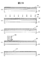
図10は、本発明の表示装置を構成する薄膜トランジスタ基板の一例を模式的に説明する平面図である。この薄膜トランジスタ基板(低温ポリシリコンTFT基板)は、ガラス基板601上に画素領域602、周辺回路(映像信号駆動回路(信号処理回路603、水平方向走査回路604)、走査信号駆動回路(垂直方向走査回路605)、昇圧回路等のその他の周辺回路606)、入力パッド607が配置される。
FIG. 10 is a plan view schematically illustrating an example of a thin film transistor substrate constituting the display device of the present invention. The thin film transistor substrate (low-temperature polysilicon TFT substrate) includes a
高速動作が必要な信号処理回路603、水平方向走査回路604、その他の周辺回路606には擬似単結晶シリコン半導体をチャネル領域に用いた薄膜トランジスタを形成する。その他の回路部である画素領域602、垂直方向走査回路605には多結晶シリコン半導体をチャネル領域に用いた薄膜トランジスタを形成する。但し、垂直方向走査回路605や画素領域602にも擬似単結晶を用いても良い。また、信号処理回路603、水平方向走査回路604、その他の周辺回路606にも通常の多結晶を用いても良い。尚、1つの回路中に通常の多結晶を用いた薄膜トランジスタと擬似単結晶を用いた薄膜トランジスタの両者を混在させても良い。
Thin film transistors using pseudo single crystal silicon semiconductors as channel regions are formed in the
次に、本発明による表示装置の実施例を実施例4として説明する。図11は、本発明による表示装置の実施例としての液晶表示装置を説明する模式図である。ガラス基板5011上に、マトリクス状に配置された複数の画素電極5031、上記画素電極に表示信号を入力する回路5071及び5111、及び画像表示のために必要なその他の周辺回路群5180を形成し、配向膜OR5190を印刷法により塗布してアクティブ・マトリクス基板とする。
Next, an embodiment of a display device according to the present invention will be described as a fourth embodiment. FIG. 11 is a schematic diagram for explaining a liquid crystal display device as an embodiment of the display device according to the present invention. On a
一方、ガラス基板5211上に対向電極5212、カラーフィルタ5213、配向膜5214を同様に塗布したカラーフィルタ基板を用意し、アクティブ・マトリクス基板と貼り合わせる。対向する配向膜5190と5214の間に、液晶5215を、真空注入により充填し、封止剤5216により液晶を封止する。その後、ガラス基板5011とガラス基板5211の外面に偏光板5217、5218をそれぞれ貼り付ける。そして、アクティブ・マトリクス基板の背面にバックライト5219を配置して液晶表示装置が完成する。
On the other hand, a color filter substrate in which a
なお、ここでは、アクティブ・マトリクス基板の対向基板側にカラーフィルタを形成した液晶表示装置を例としたが、アクティブ・マトリクス基板側にカラーフィルタを形成した形式の液晶表示装置にも同様に適用できる。また、図11には、ガラス基板5211に対向電極5212、カラーフィルタ5213、配向膜5214をこの順で形成したカラーフィルタ基板を示したが、ガラス基板5211にカラーフィルタを形成し、その上に対向電極5212を成膜し、最上層に配向膜5214を形成した構造のカラーフィルタ基板とすることもできる。カラーフィルタの形成位置やカラーフィルタ基板の構造は本発明の思想に直接関係するものでない。
Here, a liquid crystal display device in which a color filter is formed on the counter substrate side of the active matrix substrate is taken as an example, but the present invention can be similarly applied to a liquid crystal display device in which a color filter is formed on the active matrix substrate side. . FIG. 11 shows a color filter substrate in which a
本実施例によれば、画素とこの画素を駆動する駆動回路およびその他の周辺回路を、それらの要求特性に応じてアクティブ・マトリクス基板上に直接形成することが可能となり、画素領域を拡大した、高速、高解像度を有する表示品質の良好な液晶表示装置を得ることができる。 According to this embodiment, it is possible to directly form a pixel, a driving circuit for driving the pixel, and other peripheral circuits on the active matrix substrate according to their required characteristics, and the pixel area is enlarged. A liquid crystal display device having high speed and high resolution and good display quality can be obtained.
以上説明した本発明は、液晶表示装置に限るものではなく、有機EL表示装置、その他のアクティブ・マトリクス型の各種表示装置に同様に適用できる。 The present invention described above is not limited to a liquid crystal display device, but can be similarly applied to an organic EL display device and other various active matrix display devices.
また、薄膜トランジスタのチャネル領域の半導体層への不純物のドープによる閾値制御に関し、実施例ではn型の薄膜トランジスタに対してはB+を、p型の薄膜トランジスタに対してはP+を用いているが、チャネル領域にドープされる不純物は薄膜トランジスタの導電型の決定とは無関係であるため、必要に応じてn型の薄膜トランジスタに対してはP+を、p型の薄膜トランジスタに対してはB+を用いることもできる。 In addition, regarding the threshold control by doping impurities into the semiconductor layer in the channel region of the thin film transistor, B + is used for the n-type thin film transistor and P + is used for the p-type thin film transistor. Impurities doped in the channel region are irrelevant to determining the conductivity type of the thin film transistor, so use P + for n-type thin film transistors and B + for p-type thin film transistors as necessary. You can also.
101・・・ガラス基板、102・・・SiN層、103・・・SiO2層、104・・・a−Si膜、105・・・ドーパント、106・・・レーザ、107・・・p−Si膜、108・・・ドーパント、109・・・レーザ、110・・・p−Si膜、112・・・チャネル層、113・・・ゲート絶縁膜、114・・・ゲートメタル層、115・・・ホトレジスト、116・・・ゲート電極、118・・・ソース・ドレイン領域、120・・・LDD領域、121・・・層間絶縁膜、122・・・コンタクトホール、123・・・バリアメタル、124・・・アルミニューム層、125・・・キャップメタル、126・・・パッシベーション膜。
101 ... glass substrate, 102 ... SiN layer, 103 ... SiO 2 layer, 104 ... a-Si film, 105 ... dopant, 106 ... laser, 107 ... p-
Claims (14)
半導体膜を形成する半導体膜形成工程と、
前記第1の領域および前記第2の領域の前記半導体膜を熱処理することにより、前記第1の領域および前記第2の領域の前記半導体膜結晶化と前記第1の不純物の活性化とを行う第1の結晶化工程と、
前記第1の結晶化工程よりも後に、前記第1の領域および前記第2の領域の前記半導体膜に閾値制御用の第2の不純物の打ち込みを行う第2の不純物打ち込み工程と、
前記第1の領域および前記第2の領域の前記半導体膜のうち、前記第2の領域の前記半導体膜のみを熱処理することにより、前記第2の領域の半導体膜の結晶化と前記第2の不純物の結晶化とを行う第2の結晶化工程とを有することを特徴とする表示装置の製造方法。 A display having a first thin film transistor having a first threshold value formed in a first region and a second thin film transistor having a second threshold value different from the first threshold value formed in a second region A device manufacturing method comprising:
A semiconductor film forming step of forming a semiconductor film;
The semiconductor film in the first region and the second region is crystallized and the first impurity is activated by heat-treating the semiconductor film in the first region and the second region. A first crystallization step;
A second impurity implantation step of implanting a second impurity for threshold control into the semiconductor film in the first region and the second region after the first crystallization step;
By heat-treating only the semiconductor film in the second region among the semiconductor films in the first region and the second region, crystallization of the semiconductor film in the second region and the second region are performed. A method for manufacturing a display device, comprising: a second crystallization step of crystallization of impurities.
After implanting the first impurity through the insulating film, removing the insulating film, removing the insulating film, forming a surface oxide film on the surface of the semiconductor film, and forming the surface oxide film The method for manufacturing a display device according to claim 1, wherein the first crystallization step is performed.
Priority Applications (3)
| Application Number | Priority Date | Filing Date | Title |
|---|---|---|---|
| JP2005328865A JP5128767B2 (en) | 2005-11-14 | 2005-11-14 | Display device and manufacturing method thereof |
| US11/590,882 US7456433B2 (en) | 2005-11-14 | 2006-11-01 | Display device and fabrication method thereof |
| US12/285,997 US7727784B2 (en) | 2005-11-14 | 2008-10-17 | Display device and fabrication method thereof |
Applications Claiming Priority (1)
| Application Number | Priority Date | Filing Date | Title |
|---|---|---|---|
| JP2005328865A JP5128767B2 (en) | 2005-11-14 | 2005-11-14 | Display device and manufacturing method thereof |
Publications (3)
| Publication Number | Publication Date |
|---|---|
| JP2007134648A JP2007134648A (en) | 2007-05-31 |
| JP2007134648A5 JP2007134648A5 (en) | 2008-11-13 |
| JP5128767B2 true JP5128767B2 (en) | 2013-01-23 |
Family
ID=38039820
Family Applications (1)
| Application Number | Title | Priority Date | Filing Date |
|---|---|---|---|
| JP2005328865A Expired - Fee Related JP5128767B2 (en) | 2005-11-14 | 2005-11-14 | Display device and manufacturing method thereof |
Country Status (2)
| Country | Link |
|---|---|
| US (2) | US7456433B2 (en) |
| JP (1) | JP5128767B2 (en) |
Families Citing this family (6)
| Publication number | Priority date | Publication date | Assignee | Title |
|---|---|---|---|---|
| JP2009260044A (en) * | 2008-04-17 | 2009-11-05 | Hitachi Displays Ltd | Display device |
| US8999798B2 (en) * | 2009-12-17 | 2015-04-07 | Applied Materials, Inc. | Methods for forming NMOS EPI layers |
| KR20130009978A (en) * | 2010-02-26 | 2013-01-24 | 가부시키가이샤 한도오따이 에네루기 켄큐쇼 | Method for manufacturing semiconductor element and deposition apparatus |
| CN105632905B (en) * | 2016-01-21 | 2018-05-11 | 武汉华星光电技术有限公司 | Low-temperature polysilicon film transistor unit and preparation method thereof |
| KR102556021B1 (en) * | 2017-10-13 | 2023-07-17 | 삼성디스플레이 주식회사 | Display apparatus and manufacturing the same |
| TWI813503B (en) * | 2022-11-10 | 2023-08-21 | 友達光電股份有限公司 | Display apparatus |
Family Cites Families (13)
| Publication number | Priority date | Publication date | Assignee | Title |
|---|---|---|---|---|
| US5501989A (en) * | 1993-03-22 | 1996-03-26 | Semiconductor Energy Laboratory Co., Ltd. | Method of making semiconductor device/circuit having at least partially crystallized semiconductor layer |
| TW382164B (en) * | 1996-04-08 | 2000-02-11 | Hitachi Ltd | Semiconductor IC device with tunnel current free MOS transistors for power supply intercept of main logic |
| US5920097A (en) * | 1997-03-26 | 1999-07-06 | Advanced Micro Devices, Inc. | Compact, dual-transistor integrated circuit |
| TW408351B (en) * | 1997-10-17 | 2000-10-11 | Semiconductor Energy Lab | Semiconductor device and method of manufacturing the same |
| JP2000174282A (en) * | 1998-12-03 | 2000-06-23 | Semiconductor Energy Lab Co Ltd | Semiconductor device |
| US6737672B2 (en) * | 2000-08-25 | 2004-05-18 | Fujitsu Limited | Semiconductor device, manufacturing method thereof, and semiconductor manufacturing apparatus |
| US7045444B2 (en) * | 2000-12-19 | 2006-05-16 | Semiconductor Energy Laboratory Co., Ltd. | Method of manufacturing semiconductor device that includes selectively adding a noble gas element |
| JP4744700B2 (en) * | 2001-01-29 | 2011-08-10 | 株式会社日立製作所 | Thin film semiconductor device and image display device including thin film semiconductor device |
| JP3903761B2 (en) * | 2001-10-10 | 2007-04-11 | 株式会社日立製作所 | Laser annealing method and laser annealing apparatus |
| US6791106B2 (en) * | 2001-12-26 | 2004-09-14 | Kabushiki Kaisha Toshiba | Semiconductor device and method of manufacturing the same |
| JP4030758B2 (en) * | 2001-12-28 | 2008-01-09 | 株式会社半導体エネルギー研究所 | Method for manufacturing semiconductor device |
| JP4474108B2 (en) * | 2002-09-02 | 2010-06-02 | 株式会社 日立ディスプレイズ | Display device, manufacturing method thereof, and manufacturing apparatus |
| JP4364739B2 (en) * | 2004-07-15 | 2009-11-18 | シャープ株式会社 | Semiconductor device and manufacturing method thereof |
-
2005
- 2005-11-14 JP JP2005328865A patent/JP5128767B2/en not_active Expired - Fee Related
-
2006
- 2006-11-01 US US11/590,882 patent/US7456433B2/en not_active Expired - Fee Related
-
2008
- 2008-10-17 US US12/285,997 patent/US7727784B2/en not_active Expired - Fee Related
Also Published As
| Publication number | Publication date |
|---|---|
| US20090061575A1 (en) | 2009-03-05 |
| US20070108448A1 (en) | 2007-05-17 |
| US7456433B2 (en) | 2008-11-25 |
| JP2007134648A (en) | 2007-05-31 |
| US7727784B2 (en) | 2010-06-01 |
Similar Documents
| Publication | Publication Date | Title |
|---|---|---|
| US5834071A (en) | Method for forming a thin film transistor | |
| KR19990029581A (en) | Semiconductor device and liquid crystal display device | |
| US20060006425A1 (en) | Thin film transistor substrate and its manufacture | |
| JPH1184418A (en) | Display device | |
| JP5128767B2 (en) | Display device and manufacturing method thereof | |
| US7011911B2 (en) | Mask for polycrystallization and method of manufacturing thin film transistor using polycrystallization mask | |
| JP2677167B2 (en) | Method for manufacturing liquid crystal display device with built-in drive circuit | |
| JP2009206437A (en) | Display device and method of manufacturing the same | |
| US20050266594A1 (en) | Manufacturing method for display device | |
| JP2005260168A (en) | Device equipped with transistor, and its manufacturing method | |
| US7026201B2 (en) | Method for forming polycrystalline silicon thin film transistor | |
| JP3347340B2 (en) | Method for manufacturing thin film transistor | |
| JPH1187732A (en) | Semiconductor device and method for manufacturing the same | |
| US8759166B2 (en) | Method for manufacturing thin film transistor device | |
| JP4514862B2 (en) | Method for manufacturing semiconductor device | |
| JP4104888B2 (en) | Method for manufacturing thin film transistor device | |
| JPH09213965A (en) | Manufacture of semiconductor device | |
| JP4401667B2 (en) | Thin film semiconductor structure for annealing, annealing method for thin film semiconductor, thin film semiconductor device, method for manufacturing thin film semiconductor device, and display device. | |
| JPH07183537A (en) | Semiconductor device and manufacture thereof | |
| JP2001094108A (en) | Field effect transistor, transistor array substrate, and manufacturing method for the substrate | |
| JPH09148245A (en) | Semiconductor device and its manufacturing method | |
| KR100788993B1 (en) | Method of fabricating polycrystalline silicon thin-film transistor | |
| JPH0982970A (en) | Unsingle crystal semiconductor device and manufacture thereof | |
| JPH0982639A (en) | Semiconductor device and its manufacture | |
| JP3874825B2 (en) | Manufacturing method of semiconductor device and electro-optical device |
Legal Events
| Date | Code | Title | Description |
|---|---|---|---|
| A521 | Written amendment |
Free format text: JAPANESE INTERMEDIATE CODE: A523 Effective date: 20080926 |
|
| A621 | Written request for application examination |
Free format text: JAPANESE INTERMEDIATE CODE: A621 Effective date: 20080926 |
|
| A711 | Notification of change in applicant |
Free format text: JAPANESE INTERMEDIATE CODE: A712 Effective date: 20110218 |
|
| RD03 | Notification of appointment of power of attorney |
Free format text: JAPANESE INTERMEDIATE CODE: A7423 Effective date: 20110218 |
|
| A977 | Report on retrieval |
Free format text: JAPANESE INTERMEDIATE CODE: A971007 Effective date: 20120130 |
|
| A131 | Notification of reasons for refusal |
Free format text: JAPANESE INTERMEDIATE CODE: A131 Effective date: 20120306 |
|
| A521 | Written amendment |
Free format text: JAPANESE INTERMEDIATE CODE: A523 Effective date: 20120427 |
|
| TRDD | Decision of grant or rejection written | ||
| A01 | Written decision to grant a patent or to grant a registration (utility model) |
Free format text: JAPANESE INTERMEDIATE CODE: A01 Effective date: 20121023 |
|
| A01 | Written decision to grant a patent or to grant a registration (utility model) |
Free format text: JAPANESE INTERMEDIATE CODE: A01 |
|
| A61 | First payment of annual fees (during grant procedure) |
Free format text: JAPANESE INTERMEDIATE CODE: A61 Effective date: 20121101 |
|
| R150 | Certificate of patent or registration of utility model |
Free format text: JAPANESE INTERMEDIATE CODE: R150 Ref document number: 5128767 Country of ref document: JP Free format text: JAPANESE INTERMEDIATE CODE: R150 |
|
| FPAY | Renewal fee payment (event date is renewal date of database) |
Free format text: PAYMENT UNTIL: 20151109 Year of fee payment: 3 |
|
| R250 | Receipt of annual fees |
Free format text: JAPANESE INTERMEDIATE CODE: R250 |
|
| R250 | Receipt of annual fees |
Free format text: JAPANESE INTERMEDIATE CODE: R250 |
|
| R250 | Receipt of annual fees |
Free format text: JAPANESE INTERMEDIATE CODE: R250 |
|
| R250 | Receipt of annual fees |
Free format text: JAPANESE INTERMEDIATE CODE: R250 |
|
| R250 | Receipt of annual fees |
Free format text: JAPANESE INTERMEDIATE CODE: R250 |
|
| LAPS | Cancellation because of no payment of annual fees |