JP2017501575A - バンプ領域におけるビアパッドの配置が改良された基板 - Google Patents
バンプ領域におけるビアパッドの配置が改良された基板 Download PDFInfo
- Publication number
- JP2017501575A JP2017501575A JP2016539908A JP2016539908A JP2017501575A JP 2017501575 A JP2017501575 A JP 2017501575A JP 2016539908 A JP2016539908 A JP 2016539908A JP 2016539908 A JP2016539908 A JP 2016539908A JP 2017501575 A JP2017501575 A JP 2017501575A
- Authority
- JP
- Japan
- Prior art keywords
- substrate
- bump
- pad
- implementations
- interconnect
- Prior art date
- Legal status (The legal status is an assumption and is not a legal conclusion. Google has not performed a legal analysis and makes no representation as to the accuracy of the status listed.)
- Pending
Links
Images


Classifications
-
- H—ELECTRICITY
- H01—ELECTRIC ELEMENTS
- H01L—SEMICONDUCTOR DEVICES NOT COVERED BY CLASS H10
- H01L24/00—Arrangements for connecting or disconnecting semiconductor or solid-state bodies; Methods or apparatus related thereto
- H01L24/01—Means for bonding being attached to, or being formed on, the surface to be connected, e.g. chip-to-package, die-attach, "first-level" interconnects; Manufacturing methods related thereto
- H01L24/02—Bonding areas ; Manufacturing methods related thereto
- H01L24/03—Manufacturing methods
-
- H—ELECTRICITY
- H01—ELECTRIC ELEMENTS
- H01L—SEMICONDUCTOR DEVICES NOT COVERED BY CLASS H10
- H01L21/00—Processes or apparatus adapted for the manufacture or treatment of semiconductor or solid state devices or of parts thereof
- H01L21/02—Manufacture or treatment of semiconductor devices or of parts thereof
- H01L21/04—Manufacture or treatment of semiconductor devices or of parts thereof the devices having at least one potential-jump barrier or surface barrier, e.g. PN junction, depletion layer or carrier concentration layer
- H01L21/48—Manufacture or treatment of parts, e.g. containers, prior to assembly of the devices, using processes not provided for in a single one of the subgroups H01L21/06 - H01L21/326
- H01L21/4814—Conductive parts
- H01L21/4846—Leads on or in insulating or insulated substrates, e.g. metallisation
- H01L21/486—Via connections through the substrate with or without pins
-
- H—ELECTRICITY
- H01—ELECTRIC ELEMENTS
- H01L—SEMICONDUCTOR DEVICES NOT COVERED BY CLASS H10
- H01L23/00—Details of semiconductor or other solid state devices
- H01L23/48—Arrangements for conducting electric current to or from the solid state body in operation, e.g. leads, terminal arrangements ; Selection of materials therefor
- H01L23/488—Arrangements for conducting electric current to or from the solid state body in operation, e.g. leads, terminal arrangements ; Selection of materials therefor consisting of soldered or bonded constructions
- H01L23/498—Leads, i.e. metallisations or lead-frames on insulating substrates, e.g. chip carriers
- H01L23/49827—Via connections through the substrates, e.g. pins going through the substrate, coaxial cables
-
- H—ELECTRICITY
- H01—ELECTRIC ELEMENTS
- H01L—SEMICONDUCTOR DEVICES NOT COVERED BY CLASS H10
- H01L23/00—Details of semiconductor or other solid state devices
- H01L23/48—Arrangements for conducting electric current to or from the solid state body in operation, e.g. leads, terminal arrangements ; Selection of materials therefor
- H01L23/488—Arrangements for conducting electric current to or from the solid state body in operation, e.g. leads, terminal arrangements ; Selection of materials therefor consisting of soldered or bonded constructions
- H01L23/498—Leads, i.e. metallisations or lead-frames on insulating substrates, e.g. chip carriers
- H01L23/49838—Geometry or layout
-
- H—ELECTRICITY
- H01—ELECTRIC ELEMENTS
- H01L—SEMICONDUCTOR DEVICES NOT COVERED BY CLASS H10
- H01L24/00—Arrangements for connecting or disconnecting semiconductor or solid-state bodies; Methods or apparatus related thereto
- H01L24/01—Means for bonding being attached to, or being formed on, the surface to be connected, e.g. chip-to-package, die-attach, "first-level" interconnects; Manufacturing methods related thereto
- H01L24/02—Bonding areas ; Manufacturing methods related thereto
- H01L24/04—Structure, shape, material or disposition of the bonding areas prior to the connecting process
- H01L24/06—Structure, shape, material or disposition of the bonding areas prior to the connecting process of a plurality of bonding areas
-
- H—ELECTRICITY
- H01—ELECTRIC ELEMENTS
- H01L—SEMICONDUCTOR DEVICES NOT COVERED BY CLASS H10
- H01L24/00—Arrangements for connecting or disconnecting semiconductor or solid-state bodies; Methods or apparatus related thereto
- H01L24/01—Means for bonding being attached to, or being formed on, the surface to be connected, e.g. chip-to-package, die-attach, "first-level" interconnects; Manufacturing methods related thereto
- H01L24/10—Bump connectors ; Manufacturing methods related thereto
- H01L24/11—Manufacturing methods
-
- H—ELECTRICITY
- H01—ELECTRIC ELEMENTS
- H01L—SEMICONDUCTOR DEVICES NOT COVERED BY CLASS H10
- H01L24/00—Arrangements for connecting or disconnecting semiconductor or solid-state bodies; Methods or apparatus related thereto
- H01L24/01—Means for bonding being attached to, or being formed on, the surface to be connected, e.g. chip-to-package, die-attach, "first-level" interconnects; Manufacturing methods related thereto
- H01L24/10—Bump connectors ; Manufacturing methods related thereto
- H01L24/12—Structure, shape, material or disposition of the bump connectors prior to the connecting process
- H01L24/14—Structure, shape, material or disposition of the bump connectors prior to the connecting process of a plurality of bump connectors
-
- H—ELECTRICITY
- H01—ELECTRIC ELEMENTS
- H01L—SEMICONDUCTOR DEVICES NOT COVERED BY CLASS H10
- H01L2224/00—Indexing scheme for arrangements for connecting or disconnecting semiconductor or solid-state bodies and methods related thereto as covered by H01L24/00
- H01L2224/01—Means for bonding being attached to, or being formed on, the surface to be connected, e.g. chip-to-package, die-attach, "first-level" interconnects; Manufacturing methods related thereto
- H01L2224/02—Bonding areas; Manufacturing methods related thereto
- H01L2224/04—Structure, shape, material or disposition of the bonding areas prior to the connecting process
- H01L2224/0401—Bonding areas specifically adapted for bump connectors, e.g. under bump metallisation [UBM]
-
- H—ELECTRICITY
- H01—ELECTRIC ELEMENTS
- H01L—SEMICONDUCTOR DEVICES NOT COVERED BY CLASS H10
- H01L2224/00—Indexing scheme for arrangements for connecting or disconnecting semiconductor or solid-state bodies and methods related thereto as covered by H01L24/00
- H01L2224/01—Means for bonding being attached to, or being formed on, the surface to be connected, e.g. chip-to-package, die-attach, "first-level" interconnects; Manufacturing methods related thereto
- H01L2224/02—Bonding areas; Manufacturing methods related thereto
- H01L2224/04—Structure, shape, material or disposition of the bonding areas prior to the connecting process
- H01L2224/05—Structure, shape, material or disposition of the bonding areas prior to the connecting process of an individual bonding area
- H01L2224/0554—External layer
- H01L2224/0555—Shape
- H01L2224/05556—Shape in side view
- H01L2224/05558—Shape in side view conformal layer on a patterned surface
-
- H—ELECTRICITY
- H01—ELECTRIC ELEMENTS
- H01L—SEMICONDUCTOR DEVICES NOT COVERED BY CLASS H10
- H01L2224/00—Indexing scheme for arrangements for connecting or disconnecting semiconductor or solid-state bodies and methods related thereto as covered by H01L24/00
- H01L2224/01—Means for bonding being attached to, or being formed on, the surface to be connected, e.g. chip-to-package, die-attach, "first-level" interconnects; Manufacturing methods related thereto
- H01L2224/02—Bonding areas; Manufacturing methods related thereto
- H01L2224/07—Structure, shape, material or disposition of the bonding areas after the connecting process
- H01L2224/09—Structure, shape, material or disposition of the bonding areas after the connecting process of a plurality of bonding areas
- H01L2224/0901—Structure
- H01L2224/0903—Bonding areas having different sizes, e.g. different diameters, heights or widths
-
- H—ELECTRICITY
- H01—ELECTRIC ELEMENTS
- H01L—SEMICONDUCTOR DEVICES NOT COVERED BY CLASS H10
- H01L2224/00—Indexing scheme for arrangements for connecting or disconnecting semiconductor or solid-state bodies and methods related thereto as covered by H01L24/00
- H01L2224/01—Means for bonding being attached to, or being formed on, the surface to be connected, e.g. chip-to-package, die-attach, "first-level" interconnects; Manufacturing methods related thereto
- H01L2224/02—Bonding areas; Manufacturing methods related thereto
- H01L2224/07—Structure, shape, material or disposition of the bonding areas after the connecting process
- H01L2224/09—Structure, shape, material or disposition of the bonding areas after the connecting process of a plurality of bonding areas
- H01L2224/091—Disposition
- H01L2224/0912—Layout
-
- H—ELECTRICITY
- H01—ELECTRIC ELEMENTS
- H01L—SEMICONDUCTOR DEVICES NOT COVERED BY CLASS H10
- H01L2224/00—Indexing scheme for arrangements for connecting or disconnecting semiconductor or solid-state bodies and methods related thereto as covered by H01L24/00
- H01L2224/01—Means for bonding being attached to, or being formed on, the surface to be connected, e.g. chip-to-package, die-attach, "first-level" interconnects; Manufacturing methods related thereto
- H01L2224/10—Bump connectors; Manufacturing methods related thereto
- H01L2224/12—Structure, shape, material or disposition of the bump connectors prior to the connecting process
- H01L2224/13—Structure, shape, material or disposition of the bump connectors prior to the connecting process of an individual bump connector
- H01L2224/13001—Core members of the bump connector
- H01L2224/13099—Material
- H01L2224/131—Material with a principal constituent of the material being a metal or a metalloid, e.g. boron [B], silicon [Si], germanium [Ge], arsenic [As], antimony [Sb], tellurium [Te] and polonium [Po], and alloys thereof
- H01L2224/13138—Material with a principal constituent of the material being a metal or a metalloid, e.g. boron [B], silicon [Si], germanium [Ge], arsenic [As], antimony [Sb], tellurium [Te] and polonium [Po], and alloys thereof the principal constituent melting at a temperature of greater than or equal to 950°C and less than 1550°C
- H01L2224/13147—Copper [Cu] as principal constituent
-
- H—ELECTRICITY
- H01—ELECTRIC ELEMENTS
- H01L—SEMICONDUCTOR DEVICES NOT COVERED BY CLASS H10
- H01L2224/00—Indexing scheme for arrangements for connecting or disconnecting semiconductor or solid-state bodies and methods related thereto as covered by H01L24/00
- H01L2224/01—Means for bonding being attached to, or being formed on, the surface to be connected, e.g. chip-to-package, die-attach, "first-level" interconnects; Manufacturing methods related thereto
- H01L2224/10—Bump connectors; Manufacturing methods related thereto
- H01L2224/15—Structure, shape, material or disposition of the bump connectors after the connecting process
- H01L2224/16—Structure, shape, material or disposition of the bump connectors after the connecting process of an individual bump connector
- H01L2224/161—Disposition
- H01L2224/16151—Disposition the bump connector connecting between a semiconductor or solid-state body and an item not being a semiconductor or solid-state body, e.g. chip-to-substrate, chip-to-passive
- H01L2224/16221—Disposition the bump connector connecting between a semiconductor or solid-state body and an item not being a semiconductor or solid-state body, e.g. chip-to-substrate, chip-to-passive the body and the item being stacked
- H01L2224/16225—Disposition the bump connector connecting between a semiconductor or solid-state body and an item not being a semiconductor or solid-state body, e.g. chip-to-substrate, chip-to-passive the body and the item being stacked the item being non-metallic, e.g. insulating substrate with or without metallisation
- H01L2224/16235—Disposition the bump connector connecting between a semiconductor or solid-state body and an item not being a semiconductor or solid-state body, e.g. chip-to-substrate, chip-to-passive the body and the item being stacked the item being non-metallic, e.g. insulating substrate with or without metallisation the bump connector connecting to a via metallisation of the item
-
- H—ELECTRICITY
- H01—ELECTRIC ELEMENTS
- H01L—SEMICONDUCTOR DEVICES NOT COVERED BY CLASS H10
- H01L24/00—Arrangements for connecting or disconnecting semiconductor or solid-state bodies; Methods or apparatus related thereto
- H01L24/01—Means for bonding being attached to, or being formed on, the surface to be connected, e.g. chip-to-package, die-attach, "first-level" interconnects; Manufacturing methods related thereto
- H01L24/02—Bonding areas ; Manufacturing methods related thereto
- H01L24/04—Structure, shape, material or disposition of the bonding areas prior to the connecting process
- H01L24/05—Structure, shape, material or disposition of the bonding areas prior to the connecting process of an individual bonding area
-
- H—ELECTRICITY
- H01—ELECTRIC ELEMENTS
- H01L—SEMICONDUCTOR DEVICES NOT COVERED BY CLASS H10
- H01L24/00—Arrangements for connecting or disconnecting semiconductor or solid-state bodies; Methods or apparatus related thereto
- H01L24/01—Means for bonding being attached to, or being formed on, the surface to be connected, e.g. chip-to-package, die-attach, "first-level" interconnects; Manufacturing methods related thereto
- H01L24/10—Bump connectors ; Manufacturing methods related thereto
- H01L24/12—Structure, shape, material or disposition of the bump connectors prior to the connecting process
- H01L24/13—Structure, shape, material or disposition of the bump connectors prior to the connecting process of an individual bump connector
-
- H—ELECTRICITY
- H01—ELECTRIC ELEMENTS
- H01L—SEMICONDUCTOR DEVICES NOT COVERED BY CLASS H10
- H01L24/00—Arrangements for connecting or disconnecting semiconductor or solid-state bodies; Methods or apparatus related thereto
- H01L24/01—Means for bonding being attached to, or being formed on, the surface to be connected, e.g. chip-to-package, die-attach, "first-level" interconnects; Manufacturing methods related thereto
- H01L24/10—Bump connectors ; Manufacturing methods related thereto
- H01L24/15—Structure, shape, material or disposition of the bump connectors after the connecting process
- H01L24/16—Structure, shape, material or disposition of the bump connectors after the connecting process of an individual bump connector
-
- H—ELECTRICITY
- H01—ELECTRIC ELEMENTS
- H01L—SEMICONDUCTOR DEVICES NOT COVERED BY CLASS H10
- H01L2924/00—Indexing scheme for arrangements or methods for connecting or disconnecting semiconductor or solid-state bodies as covered by H01L24/00
- H01L2924/10—Details of semiconductor or other solid state devices to be connected
- H01L2924/11—Device type
- H01L2924/12—Passive devices, e.g. 2 terminal devices
- H01L2924/1204—Optical Diode
- H01L2924/12042—LASER
-
- H—ELECTRICITY
- H01—ELECTRIC ELEMENTS
- H01L—SEMICONDUCTOR DEVICES NOT COVERED BY CLASS H10
- H01L2924/00—Indexing scheme for arrangements or methods for connecting or disconnecting semiconductor or solid-state bodies as covered by H01L24/00
- H01L2924/30—Technical effects
- H01L2924/38—Effects and problems related to the device integration
- H01L2924/381—Pitch distance
Abstract
Description
本出願は、2014年4月11日に出願された、「Substrate Comprising Improved Via Pad Placement in Bump Area」という名称の米国特許出願第14/251,518号の優先権を主張し、米国特許出願第14/251,518号は、2013年12月20日に出願された、「Substrate Comprising Improved Via Pad Placement in Bump Area」という名称の米国仮出願第61/919,157号の優先権および利益を主張し、それらの出願は、参照により本明細書に明確に組み込まれる。
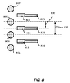
いくつかの新規の特徴は、基板と、第1のビアと、第1のバンプパッドとを含む集積デバイス(たとえば、半導体デバイス、ダイパッケージ)に関する。第1のビアは基板を横断する。第1のビアは、第1のビア横方向寸法を有する。第1のバンプパッドは、基板の表面上に位置する。第1のバンプパッドは、第1のビアに結合される。第1のバンプパッドは、第1のビア横方向寸法以下の第1のパッド横方向寸法を有する。いくつかの実装形態によれば、第1のバンプパッドは、基板のダイ領域(たとえば、フリップチップ領域)の縁部の近くに位置する周辺バンプパッドである。いくつかの実装形態では、集積デバイスは、第2のビアと第2のバンプパッドとを含む。第2のビアは基板を横断する。第2のビアは、第2のビア横方向寸法を有する。第2のバンプパッドは、基板の表面上に位置する。第2のバンプパッドは、第2のビアに結合される。第2のバンプパッドは、第2のビア横方向寸法以下の第2のパッド横方向寸法を有する。いくつかの実装形態では、第1のビアと第2のビアとの間のピッチは約40ミクロン(μm)以上である。いくつかの実装形態では、第1のビアと第2のビアとの間のピッチは約80ミクロン(μm)以下である。いくつかの実装形態では、第1のビアと第2のビアとの間のピッチは約125ミクロン(μm)以下である。いくつかの実装形態では、第1のバンプパッドと第2のバンプパッドとの間のピッチは約125ミクロン(μm)以下である。いくつかの実装形態では、ピッチは、2つの近隣の相互配線間の中心間距離として定められる。ピッチの例について図8においてさらに説明する。
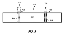
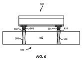
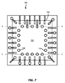
図4は、基板402といくつかの相互配線(たとえば、相互配線408、418)とを含むパッケージ基板400の平面図(たとえば、上面図)を示す。相互配線は、トレース、パッド、および/またはビアを含んでもよい。相互配線408および418は、基板402の第1の表面上に位置するパッドである。いくつかの実装形態では、相互配線408および418はビアパッドおよびバンプパッドである。相互配線408および418は、(たとえば、基板ビアを通して)基板402におけるビアに結合される。これらのビアは、相互配線408および418がビアの断面と同じサイズ(たとえば、同じ横方向寸法)を有するので平面図では見えない。いくつかの実装形態では、相互配線408および418はビアの断面よりも小さい断面を有してもよい。そのような場合、これらのビアは平面図において見えてもよい。ビアの例について図5においてさらに説明する。
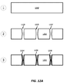
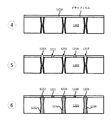
図12(図12A〜図12Cを含む)は、バンプ領域の下方にビアを含む基板を設ける/製造する/作製するための例示的なシーケンスを示す。説明を明快にしかつ簡略化することを目的として、図12A〜図12Cのプロセスが、基板を製造するすべてのステップおよび/または段階を含むとは限らないことに留意されたい。さらに、いくつかの事例では、プロセスの説明を簡単にするために、いくつかのステップおよび/または段階が単一のステップおよび/または段階に結合されている場合がある。図12A〜図12Cのパターンの形状、パターンフィーチャ、構成要素(たとえば、複合材料導電性トレース、ビア)は、概念的な例にすぎず、パターンの実際の形状および形態、パターンフィーチャ、ならびに構成要素を表すとは限らないことにも留意されたい。いくつかの実装形態では、図12A〜図12Cのシーケンスは、本開示において説明する寸法(たとえば、図8において説明した寸法)を有するトレース、ビア、および/またはパッドを作製することができるプロセスを示す。
図13は、パッケージ基板の投影図(たとえば、側面図)を示す。図13に示すように、パッケージ1300は、基板1302と、ダイ1304と、はんだレジスト層1306と、アンダーフィル1308とを含む。いくつかの実装形態では、ダイ1304はフリップチップである。
図14は、バンプ領域の下方にビアを含む基板を設ける/製造する/作製するための例示的な方法を示す。説明を明快にしかつ簡略化することを目的として、図14のプロセスが、基板を製造するすべてのステップおよび/または段階を含むとは限らないことに留意されたい。さらに、いくつかの事例では、プロセスの説明を簡単にするために、いくつかのステップおよび/または段階が単一のステップおよび/または段階に結合されている場合がある。図14のパターンの形状、パターンフィーチャ、構成要素(たとえば、複合材料導電性トレース、ビア)は、概念的な例にすぎず、パターンの実際の形状および形態、パターンフィーチャ、ならびに構成要素を表すとは限らないことにも留意されたい。
図15は、基板を製造するためのモディファイドセミアディティブ法(mSAP)パターニングプロセスの流れ図を示す。図15について、いくつかの実装形態のmSAPプロセス時の基板の層(たとえば、コア層、プリプレグ層)のシーケンスを示す図16を参照しながら説明する。
図20は、上述の集積デバイス(たとえば、半導体デバイス)、集積回路、ダイ、インターポーザ、および/またはパッケージのうちのいずれかと統合される場合がある様々な電子デバイスを示す。たとえば、モバイル電話2002、ラップトップコンピュータ2004、および固定位置端末2006が、本明細書で説明する集積回路デバイス2000を含んでもよい。集積デバイス2000は、たとえば、本明細書で説明する集積デバイス、集積回路、ダイ、またはパッケージのうちのいずれかであってもよい。図20に示すデバイス2002、2004、2006は例示にすぎない。他の電子デバイスはまた、限定はされないが、モバイルデバイス、ハンドヘルドパーソナル通信システム(PCS)ユニット、携帯情報端末などのポータブルデータユニット、GPS対応デバイス、ナビゲーションデバイス、セットトップボックス、音楽プレーヤ、ビデオプレーヤ、エンターテイメントユニット、メータ読取り機器などの固定位置データユニット、通信デバイス、スマートフォン、タブレットコンピュータ、またはデータもしくはコンピュータ命令を記憶し、もしくは取り出す任意の他のデバイス、またはそれらの任意の組合せを含む、集積デバイス2000を特徴付けてもよい。
102 基板
104 第1のパッド
106 第1のトレース
108 第2のパッド
114 第3のパッド
116 第2のトレース
118 第4のパッド
300 フリップチップ
302 第1のバンプ
304 第2のバンプ
400 パッケージ基板
402 基板
404 第1の相互配線
408 相互配線
418 相互配線
420 ダイ領域
510 第1のバンプ領域
520 第2のバンプ領域
600 ダイ
602 第1のバンプ
604 第2のバンプ
700 パッケージ基板
702 基板
708 相互配線
718 相互配線
720 ダイ領域
801 パッド
803 パッド
805 パッド
807 パッド
811 第1のバンプパッド
813 第2のバンプパッド
815 第3のバンプパッド
821 第3の相互配線
823 第2の相互配線
825 第3の相互配線
830 第1のピッチ
832 第2のピッチ
900 パッケージ
902 基板
904 ダイ
906 はんだレジスト層
908 アンダーフィル
920 第1の相互配線
922 第1のパッド
924 第2の相互配線
926 第2のパッド
928 第3の相互配線
930 第1のバンプ
932 第2のバンプ
934 第3のバンプ
936 第4のバンプ
938 第5のバンプ
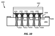
1000 パッケージ
1002 パッケージ基板
1004 ダイ
1006 はんだレジスト層
1008 アンダーフィル
1020 第1の相互配線
1022 第2の相互配線
1024 第3の相互配線
1026 第4の相互配線
1028 第5の相互配線
1030 第1のバンプ
1032 第2のバンプ
1034 第3のバンプ
1036 第4のバンプ
1038 第5のバンプ
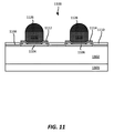
1100 ダイ
1101 基板
1104 第1のパッド
1106 第2のパッド
1108 パッシベーション層
1110 第1の絶縁層
1111 ダイ
1116 第1の相互配線
1118 第2の相互配線
1126 第1のはんだボール
1128 第2のはんだボール
1202 基板
1203 第1のキャビティ
1204 第1の金属層
1205 第2のキャビティ
1206 第2の金属層
1207 第3のキャビティ
1208 第3の金属層
1210 ドライフィルム層
1211 第4の開口部
1213 第1の開口部
1215 第2の開口部
1217 第3の開口部
1219 第5の開口部
1221 第4の相互配線
1222 第1の相互配線
1224 第2の相互配線
1226 第3の相互配線
1229 第5の相互配線
1232 ビア
1240 はんだレジスト層
1250 ダイ
1260 アンダーフィル
1300 パッケージ
1302 基板
1304 ダイ
1306 はんだレジスト層
1308 アンダーフィル
1311 第1の金属層
1313 第2の金属層
1320 第1の相互配線
1322 第2の相互配線
1324 第3の相互配線
1326 第4の相互配線
1328 第5の相互配線
1330 第1のバンプ
1332 第2のバンプ
1334 第3のバンプ
1336 第4のバンプ
1338 第5のバンプ
1402 基板
1403 第1のキャビティ
1405 第2のキャビティ
1407 第3のキャビティ
1602 誘電体層
1604 薄い銅層
1606 DFR
1608 開口部
1802 誘電体
1804 プライマ
1806 銅箔
1808 銅シード層
1810 DFR
1812 開口部
2000 集積デバイス
2002 モバイル電話
2004 ラップトップコンピュータ
2006 固定位置端末
Claims (20)
- 集積デバイスであって、
基板と、
前記基板を横断し、第1のビア寸法を有する第1のビアと、
前記基板の表面上に位置し、前記第1のビアに結合され、前記第1のビア寸法以下の第1のパッド寸法を有する第1のバンプパッドとを備える集積デバイス。 - 前記基板を横断し、第2のビア寸法を有する第2のビアと、
前記基板の前記表面上に位置し、前記第2のビアに結合され、前記第2のビア寸法以下の第2のパッド寸法を有する第2のバンプパッドとをさらに備える、請求項1に記載の集積デバイス。 - 前記第1のビアと前記第2のビアとの間のピッチは約80ミクロン(μm)以下である、請求項2に記載の集積デバイス。
- 前記第1のビアと前記第2のビアとの間のピッチは約125ミクロン(μm)以下である、請求項2に記載の集積デバイス。
- 前記第1のバンプパッドは、ダイの相互配線に結合するように構成される、請求項1に記載の集積デバイス。
- 前記第1のバンプパッドは、前記基板のダイ領域の縁部の近くに位置する周辺バンプパッドである、請求項1に記載の集積デバイス。
- 前記第1のバンプパッドは、ダイからの第1のバンプに結合するように構成される、請求項1に記載の集積デバイス。
- 前記第1のバンプは、第1のアンダーバンプメタライゼーション(UBM)層と、第1の相互配線ピラーと、第1のはんだボールとを含む、請求項7に記載の集積デバイス。
- 前記基板が、少なくとも誘電体、ガラス、セラミック、および/またはシリコンのうちの1つを含む、請求項1に記載の集積デバイス。
- 前記集積デバイスは、音楽プレーヤ、ビデオプレーヤ、エンターテイメントユニット、ナビゲーションデバイス、通信デバイス、モバイルデバイス、モバイルフォン、スマートフォン、携帯情報端末、固定位置端末、タブレットコンピュータ、および/またはラップトップコンピュータのうちの少なくとも1つに組み込まれる、請求項1に記載の集積デバイス。
- 集積デバイスを作製するための方法であって、
基板を形成するステップと、
前記基板を横断する第1のビアを形成するステップであって、前記第1のビアは第1のビア寸法を有するステップと、
前記基板の表面上に、前記第1のビアに結合されるように第1のバンプパッドを形成するステップであって、前記第1のバンプパッドは、前記第1のビア寸法以下の第1のパッド寸法を有するステップとを含む方法。 - 前記基板を横断する第2のビアを形成するステップであって、前記第2のビアは第2のビア寸法を有するステップと、
前記基板の前記表面上に、前記第2のビアに結合されるように第2のバンプパッドを形成するステップであって、前記第2のバンプパッドは、前記第2のビア寸法以下の第2のパッド寸法を有するステップとをさらに含む、請求項11に記載の方法。 - 前記第1のビアと前記第2のビアとの間のピッチは約80ミクロン(μm)以下である、請求項12に記載の方法。
- 前記第1のビアと前記第2のビアとの間のピッチは約125ミクロン(μm)以下である、請求項12に記載の方法。
- 前記第1のバンプパッドは、ダイの相互配線に結合するように構成される、請求項11に記載の方法。
- 前記第1のバンプパッドは、前記基板のダイ領域の縁部の近くに位置する周辺バンプパッドである、請求項11に記載の方法。
- 前記第1のバンプパッドは、ダイからの第1のバンプに結合するように構成される、請求項11に記載の方法。
- 前記第1のバンプは、第1のアンダーバンプメタライゼーション(UBM)層と、第1の相互配線ピラーと、第1のはんだボールとを含む、請求項17に記載の方法。
- 前記基板は、少なくとも誘電体、ガラス、セラミック、および/またはシリコンのうちの1つを含む、請求項11に記載の方法。
- 前記集積デバイスは、音楽プレーヤ、ビデオプレーヤ、エンターテイメントユニット、ナビゲーションデバイス、通信デバイス、モバイルデバイス、モバイルフォン、スマートフォン、携帯情報端末、固定位置端末、タブレットコンピュータ、および/またはラップトップコンピュータのうちの少なくとも1つに組み込まれる、請求項11に記載の方法。
Applications Claiming Priority (5)
| Application Number | Priority Date | Filing Date | Title |
|---|---|---|---|
| US201361919157P | 2013-12-20 | 2013-12-20 | |
| US61/919,157 | 2013-12-20 | ||
| US14/251,518 | 2014-04-11 | ||
| US14/251,518 US9466578B2 (en) | 2013-12-20 | 2014-04-11 | Substrate comprising improved via pad placement in bump area |
| PCT/US2014/070940 WO2015095385A1 (en) | 2013-12-20 | 2014-12-17 | Substrate comprising improved via pad placement in bump area |
Publications (2)
| Publication Number | Publication Date |
|---|---|
| JP2017501575A true JP2017501575A (ja) | 2017-01-12 |
| JP2017501575A5 JP2017501575A5 (ja) | 2017-03-16 |
Family
ID=53400887
Family Applications (1)
| Application Number | Title | Priority Date | Filing Date |
|---|---|---|---|
| JP2016539908A Pending JP2017501575A (ja) | 2013-12-20 | 2014-12-17 | バンプ領域におけるビアパッドの配置が改良された基板 |
Country Status (5)
| Country | Link |
|---|---|
| US (1) | US9466578B2 (ja) |
| EP (1) | EP3084826A1 (ja) |
| JP (1) | JP2017501575A (ja) |
| CN (1) | CN105830213B (ja) |
| WO (1) | WO2015095385A1 (ja) |
Cited By (1)
| Publication number | Priority date | Publication date | Assignee | Title |
|---|---|---|---|---|
| WO2019065656A1 (ja) * | 2017-09-29 | 2019-04-04 | 大日本印刷株式会社 | 貫通電極基板及び貫通電極基板を用いた半導体装置 |
Families Citing this family (4)
| Publication number | Priority date | Publication date | Assignee | Title |
|---|---|---|---|---|
| TWI504320B (zh) * | 2014-06-17 | 2015-10-11 | 矽品精密工業股份有限公司 | 線路結構及其製法 |
| US20170018448A1 (en) * | 2015-07-15 | 2017-01-19 | Chip Solutions, LLC | Semiconductor device and method |
| US10895028B2 (en) | 2015-12-14 | 2021-01-19 | Dupont Industrial Biosciences Usa, Llc | Nonwoven glucan webs |
| JP2017130823A (ja) * | 2016-01-21 | 2017-07-27 | 京セラ株式会社 | 圧電発振器及びその製造方法 |
Citations (8)
| Publication number | Priority date | Publication date | Assignee | Title |
|---|---|---|---|---|
| JPH09199535A (ja) * | 1996-01-16 | 1997-07-31 | Hitachi Ltd | 半導体集積回路の電極構造およびそのパッケージ形成方法 |
| JPH11150158A (ja) * | 1997-11-19 | 1999-06-02 | Shinko Electric Ind Co Ltd | 多層回路基板 |
| US20010008778A1 (en) * | 1999-09-23 | 2001-07-19 | International Business Machines Corporation | Temporary attach article and method for temporary attach of devices to a substrate |
| US20040155347A1 (en) * | 2003-02-07 | 2004-08-12 | Kwun-Yao Ho | Vertical routing structure |
| JP2009135147A (ja) * | 2007-11-28 | 2009-06-18 | Shinko Electric Ind Co Ltd | 配線基板及び電子素子の接続構造及び電子装置 |
| JP2011222901A (ja) * | 2010-04-14 | 2011-11-04 | Renesas Electronics Corp | 半導体装置 |
| US20130134581A1 (en) * | 2011-11-30 | 2013-05-30 | Taiwan Semiconductor Manufacturing Company, Ltd. | Planarized bumps for underfill control |
| US20130264720A1 (en) * | 2012-04-09 | 2013-10-10 | Samsung Electronics Co., Ltd. | Semiconductor Chips Having Through Silicon Vias and Related Fabrication Methods and Semiconductor Packages |
Family Cites Families (14)
| Publication number | Priority date | Publication date | Assignee | Title |
|---|---|---|---|---|
| EP0851724B1 (en) | 1996-12-26 | 2003-10-22 | Matsushita Electric Industrial Co., Ltd. | Printed circuit board and electric components |
| JP3386977B2 (ja) * | 1997-06-05 | 2003-03-17 | 新光電気工業株式会社 | 多層回路基板 |
| US6940176B2 (en) | 2002-05-21 | 2005-09-06 | United Microelectronics Corp. | Solder pads for improving reliability of a package |
| WO2004047167A1 (ja) | 2002-11-21 | 2004-06-03 | Nec Corporation | 半導体装置、配線基板および配線基板製造方法 |
| JP3986989B2 (ja) * | 2003-03-27 | 2007-10-03 | 松下電器産業株式会社 | 半導体装置 |
| US7939941B2 (en) | 2007-06-27 | 2011-05-10 | Taiwan Semiconductor Manufacturing Company, Ltd. | Formation of through via before contact processing |
| WO2009048154A1 (ja) | 2007-10-12 | 2009-04-16 | Nec Corporation | 半導体装置及びその設計方法 |
| JP2009260098A (ja) | 2008-04-18 | 2009-11-05 | Shinko Electric Ind Co Ltd | 配線基板及び半導体装置 |
| US8227295B2 (en) | 2008-10-16 | 2012-07-24 | Texas Instruments Incorporated | IC die having TSV and wafer level underfill and stacked IC devices comprising a workpiece solder connected to the TSV |
| US8344503B2 (en) * | 2008-11-25 | 2013-01-01 | Freescale Semiconductor, Inc. | 3-D circuits with integrated passive devices |
| TWI420643B (zh) | 2008-12-16 | 2013-12-21 | Powertech Technology Inc | 具有矽穿孔之晶片結構、形成方法以及使用該晶片結構之堆疊構造 |
| US8791549B2 (en) * | 2009-09-22 | 2014-07-29 | Taiwan Semiconductor Manufacturing Company, Ltd. | Wafer backside interconnect structure connected to TSVs |
| US9167694B2 (en) | 2010-11-02 | 2015-10-20 | Georgia Tech Research Corporation | Ultra-thin interposer assemblies with through vias |
| GB2485830A (en) * | 2010-11-26 | 2012-05-30 | Cambridge Silicon Radio Ltd | Stacked multi-chip package using encapsulated electroplated pillar conductors; also able to include MEMS elements |
-
2014
- 2014-04-11 US US14/251,518 patent/US9466578B2/en not_active Expired - Fee Related
- 2014-12-17 EP EP14825040.0A patent/EP3084826A1/en not_active Withdrawn
- 2014-12-17 JP JP2016539908A patent/JP2017501575A/ja active Pending
- 2014-12-17 WO PCT/US2014/070940 patent/WO2015095385A1/en active Application Filing
- 2014-12-17 CN CN201480069410.XA patent/CN105830213B/zh not_active Expired - Fee Related
Patent Citations (8)
| Publication number | Priority date | Publication date | Assignee | Title |
|---|---|---|---|---|
| JPH09199535A (ja) * | 1996-01-16 | 1997-07-31 | Hitachi Ltd | 半導体集積回路の電極構造およびそのパッケージ形成方法 |
| JPH11150158A (ja) * | 1997-11-19 | 1999-06-02 | Shinko Electric Ind Co Ltd | 多層回路基板 |
| US20010008778A1 (en) * | 1999-09-23 | 2001-07-19 | International Business Machines Corporation | Temporary attach article and method for temporary attach of devices to a substrate |
| US20040155347A1 (en) * | 2003-02-07 | 2004-08-12 | Kwun-Yao Ho | Vertical routing structure |
| JP2009135147A (ja) * | 2007-11-28 | 2009-06-18 | Shinko Electric Ind Co Ltd | 配線基板及び電子素子の接続構造及び電子装置 |
| JP2011222901A (ja) * | 2010-04-14 | 2011-11-04 | Renesas Electronics Corp | 半導体装置 |
| US20130134581A1 (en) * | 2011-11-30 | 2013-05-30 | Taiwan Semiconductor Manufacturing Company, Ltd. | Planarized bumps for underfill control |
| US20130264720A1 (en) * | 2012-04-09 | 2013-10-10 | Samsung Electronics Co., Ltd. | Semiconductor Chips Having Through Silicon Vias and Related Fabrication Methods and Semiconductor Packages |
Cited By (3)
| Publication number | Priority date | Publication date | Assignee | Title |
|---|---|---|---|---|
| WO2019065656A1 (ja) * | 2017-09-29 | 2019-04-04 | 大日本印刷株式会社 | 貫通電極基板及び貫通電極基板を用いた半導体装置 |
| JPWO2019065656A1 (ja) * | 2017-09-29 | 2020-11-19 | 大日本印刷株式会社 | 貫通電極基板及び貫通電極基板を用いた半導体装置 |
| JP7180605B2 (ja) | 2017-09-29 | 2022-11-30 | 大日本印刷株式会社 | 貫通電極基板及び貫通電極基板を用いた半導体装置 |
Also Published As
| Publication number | Publication date |
|---|---|
| WO2015095385A1 (en) | 2015-06-25 |
| US9466578B2 (en) | 2016-10-11 |
| CN105830213A (zh) | 2016-08-03 |
| US20150179590A1 (en) | 2015-06-25 |
| CN105830213B (zh) | 2019-09-10 |
| EP3084826A1 (en) | 2016-10-26 |
Similar Documents
| Publication | Publication Date | Title |
|---|---|---|
| US11443970B2 (en) | Methods of forming a package substrate | |
| JP6240342B2 (ja) | 表面相互配線と無電解フィルを含むキャビティとを備えるパッケージ基板 | |
| KR20180044905A (ko) | 리소-에칭가능 층에 브리지를 포함하는 통합 디바이스 패키지 | |
| US9368566B2 (en) | Package on package (PoP) integrated device comprising a capacitor in a substrate | |
| CN107004612B (zh) | 在基板与管芯之间包括光敏填料的集成器件封装 | |
| KR101255954B1 (ko) | 인쇄회로기판 및 인쇄회로기판 제조 방법 | |
| US10651160B2 (en) | Low profile integrated package | |
| JP2017501575A (ja) | バンプ領域におけるビアパッドの配置が改良された基板 | |
| TW202017135A (zh) | 包括核心層的嵌入式跡線襯底(ets)中的高密度互連 | |
| US9355898B2 (en) | Package on package (PoP) integrated device comprising a plurality of solder resist layers | |
| US20160183379A1 (en) | Substrate comprising an embedded capacitor | |
| US20160316557A1 (en) | Printed circuit board, manufacturing method thereof and electronic component module | |
| US9807884B2 (en) | Substrate comprising embedded elongated capacitor | |
| US20160198568A1 (en) | Printed circuit board and electronic component module | |
| TW201921590A (zh) | 具有保留互連部分之精細節距及間隔互連 | |
| CN104392937A (zh) | 增加bbul封装中的i/o密度和降低层数的方法 | |
| US10157824B2 (en) | Integrated circuit (IC) package and package substrate comprising stacked vias | |
| JP2008305952A (ja) | 高密度細線実装構造及びその製造方法 |
Legal Events
| Date | Code | Title | Description |
|---|---|---|---|
| A521 | Request for written amendment filed |
Free format text: JAPANESE INTERMEDIATE CODE: A523 Effective date: 20160621 |
|
| A521 | Request for written amendment filed |
Free format text: JAPANESE INTERMEDIATE CODE: A523 Effective date: 20170209 |
|
| A621 | Written request for application examination |
Free format text: JAPANESE INTERMEDIATE CODE: A621 Effective date: 20170209 |
|
| A871 | Explanation of circumstances concerning accelerated examination |
Free format text: JAPANESE INTERMEDIATE CODE: A871 Effective date: 20170209 |
|
| A975 | Report on accelerated examination |
Free format text: JAPANESE INTERMEDIATE CODE: A971005 Effective date: 20170215 |
|
| A131 | Notification of reasons for refusal |
Free format text: JAPANESE INTERMEDIATE CODE: A131 Effective date: 20170306 |
|
| A601 | Written request for extension of time |
Free format text: JAPANESE INTERMEDIATE CODE: A601 Effective date: 20170606 |
|
| A02 | Decision of refusal |
Free format text: JAPANESE INTERMEDIATE CODE: A02 Effective date: 20171120 |