JP2017501575A - Substrate with improved via pad placement in the bump area - Google Patents
Substrate with improved via pad placement in the bump area Download PDFInfo
- Publication number
- JP2017501575A JP2017501575A JP2016539908A JP2016539908A JP2017501575A JP 2017501575 A JP2017501575 A JP 2017501575A JP 2016539908 A JP2016539908 A JP 2016539908A JP 2016539908 A JP2016539908 A JP 2016539908A JP 2017501575 A JP2017501575 A JP 2017501575A
- Authority
- JP
- Japan
- Prior art keywords
- substrate
- bump
- pad
- implementations
- interconnect
- Prior art date
- Legal status (The legal status is an assumption and is not a legal conclusion. Google has not performed a legal analysis and makes no representation as to the accuracy of the status listed.)
- Pending
Links
Images


Classifications
-
- H—ELECTRICITY
- H01—ELECTRIC ELEMENTS
- H01L—SEMICONDUCTOR DEVICES NOT COVERED BY CLASS H10
- H01L24/00—Arrangements for connecting or disconnecting semiconductor or solid-state bodies; Methods or apparatus related thereto
- H01L24/01—Means for bonding being attached to, or being formed on, the surface to be connected, e.g. chip-to-package, die-attach, "first-level" interconnects; Manufacturing methods related thereto
- H01L24/02—Bonding areas ; Manufacturing methods related thereto
- H01L24/03—Manufacturing methods
-
- H—ELECTRICITY
- H01—ELECTRIC ELEMENTS
- H01L—SEMICONDUCTOR DEVICES NOT COVERED BY CLASS H10
- H01L21/00—Processes or apparatus adapted for the manufacture or treatment of semiconductor or solid state devices or of parts thereof
- H01L21/02—Manufacture or treatment of semiconductor devices or of parts thereof
- H01L21/04—Manufacture or treatment of semiconductor devices or of parts thereof the devices having at least one potential-jump barrier or surface barrier, e.g. PN junction, depletion layer or carrier concentration layer
- H01L21/48—Manufacture or treatment of parts, e.g. containers, prior to assembly of the devices, using processes not provided for in a single one of the subgroups H01L21/06 - H01L21/326
- H01L21/4814—Conductive parts
- H01L21/4846—Leads on or in insulating or insulated substrates, e.g. metallisation
- H01L21/486—Via connections through the substrate with or without pins
-
- H—ELECTRICITY
- H01—ELECTRIC ELEMENTS
- H01L—SEMICONDUCTOR DEVICES NOT COVERED BY CLASS H10
- H01L23/00—Details of semiconductor or other solid state devices
- H01L23/48—Arrangements for conducting electric current to or from the solid state body in operation, e.g. leads, terminal arrangements ; Selection of materials therefor
- H01L23/488—Arrangements for conducting electric current to or from the solid state body in operation, e.g. leads, terminal arrangements ; Selection of materials therefor consisting of soldered or bonded constructions
- H01L23/498—Leads, i.e. metallisations or lead-frames on insulating substrates, e.g. chip carriers
- H01L23/49827—Via connections through the substrates, e.g. pins going through the substrate, coaxial cables
-
- H—ELECTRICITY
- H01—ELECTRIC ELEMENTS
- H01L—SEMICONDUCTOR DEVICES NOT COVERED BY CLASS H10
- H01L23/00—Details of semiconductor or other solid state devices
- H01L23/48—Arrangements for conducting electric current to or from the solid state body in operation, e.g. leads, terminal arrangements ; Selection of materials therefor
- H01L23/488—Arrangements for conducting electric current to or from the solid state body in operation, e.g. leads, terminal arrangements ; Selection of materials therefor consisting of soldered or bonded constructions
- H01L23/498—Leads, i.e. metallisations or lead-frames on insulating substrates, e.g. chip carriers
- H01L23/49838—Geometry or layout
-
- H—ELECTRICITY
- H01—ELECTRIC ELEMENTS
- H01L—SEMICONDUCTOR DEVICES NOT COVERED BY CLASS H10
- H01L24/00—Arrangements for connecting or disconnecting semiconductor or solid-state bodies; Methods or apparatus related thereto
- H01L24/01—Means for bonding being attached to, or being formed on, the surface to be connected, e.g. chip-to-package, die-attach, "first-level" interconnects; Manufacturing methods related thereto
- H01L24/02—Bonding areas ; Manufacturing methods related thereto
- H01L24/04—Structure, shape, material or disposition of the bonding areas prior to the connecting process
- H01L24/06—Structure, shape, material or disposition of the bonding areas prior to the connecting process of a plurality of bonding areas
-
- H—ELECTRICITY
- H01—ELECTRIC ELEMENTS
- H01L—SEMICONDUCTOR DEVICES NOT COVERED BY CLASS H10
- H01L24/00—Arrangements for connecting or disconnecting semiconductor or solid-state bodies; Methods or apparatus related thereto
- H01L24/01—Means for bonding being attached to, or being formed on, the surface to be connected, e.g. chip-to-package, die-attach, "first-level" interconnects; Manufacturing methods related thereto
- H01L24/10—Bump connectors ; Manufacturing methods related thereto
- H01L24/11—Manufacturing methods
-
- H—ELECTRICITY
- H01—ELECTRIC ELEMENTS
- H01L—SEMICONDUCTOR DEVICES NOT COVERED BY CLASS H10
- H01L24/00—Arrangements for connecting or disconnecting semiconductor or solid-state bodies; Methods or apparatus related thereto
- H01L24/01—Means for bonding being attached to, or being formed on, the surface to be connected, e.g. chip-to-package, die-attach, "first-level" interconnects; Manufacturing methods related thereto
- H01L24/10—Bump connectors ; Manufacturing methods related thereto
- H01L24/12—Structure, shape, material or disposition of the bump connectors prior to the connecting process
- H01L24/14—Structure, shape, material or disposition of the bump connectors prior to the connecting process of a plurality of bump connectors
-
- H—ELECTRICITY
- H01—ELECTRIC ELEMENTS
- H01L—SEMICONDUCTOR DEVICES NOT COVERED BY CLASS H10
- H01L2224/00—Indexing scheme for arrangements for connecting or disconnecting semiconductor or solid-state bodies and methods related thereto as covered by H01L24/00
- H01L2224/01—Means for bonding being attached to, or being formed on, the surface to be connected, e.g. chip-to-package, die-attach, "first-level" interconnects; Manufacturing methods related thereto
- H01L2224/02—Bonding areas; Manufacturing methods related thereto
- H01L2224/04—Structure, shape, material or disposition of the bonding areas prior to the connecting process
- H01L2224/0401—Bonding areas specifically adapted for bump connectors, e.g. under bump metallisation [UBM]
-
- H—ELECTRICITY
- H01—ELECTRIC ELEMENTS
- H01L—SEMICONDUCTOR DEVICES NOT COVERED BY CLASS H10
- H01L2224/00—Indexing scheme for arrangements for connecting or disconnecting semiconductor or solid-state bodies and methods related thereto as covered by H01L24/00
- H01L2224/01—Means for bonding being attached to, or being formed on, the surface to be connected, e.g. chip-to-package, die-attach, "first-level" interconnects; Manufacturing methods related thereto
- H01L2224/02—Bonding areas; Manufacturing methods related thereto
- H01L2224/04—Structure, shape, material or disposition of the bonding areas prior to the connecting process
- H01L2224/05—Structure, shape, material or disposition of the bonding areas prior to the connecting process of an individual bonding area
- H01L2224/0554—External layer
- H01L2224/0555—Shape
- H01L2224/05556—Shape in side view
- H01L2224/05558—Shape in side view conformal layer on a patterned surface
-
- H—ELECTRICITY
- H01—ELECTRIC ELEMENTS
- H01L—SEMICONDUCTOR DEVICES NOT COVERED BY CLASS H10
- H01L2224/00—Indexing scheme for arrangements for connecting or disconnecting semiconductor or solid-state bodies and methods related thereto as covered by H01L24/00
- H01L2224/01—Means for bonding being attached to, or being formed on, the surface to be connected, e.g. chip-to-package, die-attach, "first-level" interconnects; Manufacturing methods related thereto
- H01L2224/02—Bonding areas; Manufacturing methods related thereto
- H01L2224/07—Structure, shape, material or disposition of the bonding areas after the connecting process
- H01L2224/09—Structure, shape, material or disposition of the bonding areas after the connecting process of a plurality of bonding areas
- H01L2224/0901—Structure
- H01L2224/0903—Bonding areas having different sizes, e.g. different diameters, heights or widths
-
- H—ELECTRICITY
- H01—ELECTRIC ELEMENTS
- H01L—SEMICONDUCTOR DEVICES NOT COVERED BY CLASS H10
- H01L2224/00—Indexing scheme for arrangements for connecting or disconnecting semiconductor or solid-state bodies and methods related thereto as covered by H01L24/00
- H01L2224/01—Means for bonding being attached to, or being formed on, the surface to be connected, e.g. chip-to-package, die-attach, "first-level" interconnects; Manufacturing methods related thereto
- H01L2224/02—Bonding areas; Manufacturing methods related thereto
- H01L2224/07—Structure, shape, material or disposition of the bonding areas after the connecting process
- H01L2224/09—Structure, shape, material or disposition of the bonding areas after the connecting process of a plurality of bonding areas
- H01L2224/091—Disposition
- H01L2224/0912—Layout
-
- H—ELECTRICITY
- H01—ELECTRIC ELEMENTS
- H01L—SEMICONDUCTOR DEVICES NOT COVERED BY CLASS H10
- H01L2224/00—Indexing scheme for arrangements for connecting or disconnecting semiconductor or solid-state bodies and methods related thereto as covered by H01L24/00
- H01L2224/01—Means for bonding being attached to, or being formed on, the surface to be connected, e.g. chip-to-package, die-attach, "first-level" interconnects; Manufacturing methods related thereto
- H01L2224/10—Bump connectors; Manufacturing methods related thereto
- H01L2224/12—Structure, shape, material or disposition of the bump connectors prior to the connecting process
- H01L2224/13—Structure, shape, material or disposition of the bump connectors prior to the connecting process of an individual bump connector
- H01L2224/13001—Core members of the bump connector
- H01L2224/13099—Material
- H01L2224/131—Material with a principal constituent of the material being a metal or a metalloid, e.g. boron [B], silicon [Si], germanium [Ge], arsenic [As], antimony [Sb], tellurium [Te] and polonium [Po], and alloys thereof
- H01L2224/13138—Material with a principal constituent of the material being a metal or a metalloid, e.g. boron [B], silicon [Si], germanium [Ge], arsenic [As], antimony [Sb], tellurium [Te] and polonium [Po], and alloys thereof the principal constituent melting at a temperature of greater than or equal to 950°C and less than 1550°C
- H01L2224/13147—Copper [Cu] as principal constituent
-
- H—ELECTRICITY
- H01—ELECTRIC ELEMENTS
- H01L—SEMICONDUCTOR DEVICES NOT COVERED BY CLASS H10
- H01L2224/00—Indexing scheme for arrangements for connecting or disconnecting semiconductor or solid-state bodies and methods related thereto as covered by H01L24/00
- H01L2224/01—Means for bonding being attached to, or being formed on, the surface to be connected, e.g. chip-to-package, die-attach, "first-level" interconnects; Manufacturing methods related thereto
- H01L2224/10—Bump connectors; Manufacturing methods related thereto
- H01L2224/15—Structure, shape, material or disposition of the bump connectors after the connecting process
- H01L2224/16—Structure, shape, material or disposition of the bump connectors after the connecting process of an individual bump connector
- H01L2224/161—Disposition
- H01L2224/16151—Disposition the bump connector connecting between a semiconductor or solid-state body and an item not being a semiconductor or solid-state body, e.g. chip-to-substrate, chip-to-passive
- H01L2224/16221—Disposition the bump connector connecting between a semiconductor or solid-state body and an item not being a semiconductor or solid-state body, e.g. chip-to-substrate, chip-to-passive the body and the item being stacked
- H01L2224/16225—Disposition the bump connector connecting between a semiconductor or solid-state body and an item not being a semiconductor or solid-state body, e.g. chip-to-substrate, chip-to-passive the body and the item being stacked the item being non-metallic, e.g. insulating substrate with or without metallisation
- H01L2224/16235—Disposition the bump connector connecting between a semiconductor or solid-state body and an item not being a semiconductor or solid-state body, e.g. chip-to-substrate, chip-to-passive the body and the item being stacked the item being non-metallic, e.g. insulating substrate with or without metallisation the bump connector connecting to a via metallisation of the item
-
- H—ELECTRICITY
- H01—ELECTRIC ELEMENTS
- H01L—SEMICONDUCTOR DEVICES NOT COVERED BY CLASS H10
- H01L24/00—Arrangements for connecting or disconnecting semiconductor or solid-state bodies; Methods or apparatus related thereto
- H01L24/01—Means for bonding being attached to, or being formed on, the surface to be connected, e.g. chip-to-package, die-attach, "first-level" interconnects; Manufacturing methods related thereto
- H01L24/02—Bonding areas ; Manufacturing methods related thereto
- H01L24/04—Structure, shape, material or disposition of the bonding areas prior to the connecting process
- H01L24/05—Structure, shape, material or disposition of the bonding areas prior to the connecting process of an individual bonding area
-
- H—ELECTRICITY
- H01—ELECTRIC ELEMENTS
- H01L—SEMICONDUCTOR DEVICES NOT COVERED BY CLASS H10
- H01L24/00—Arrangements for connecting or disconnecting semiconductor or solid-state bodies; Methods or apparatus related thereto
- H01L24/01—Means for bonding being attached to, or being formed on, the surface to be connected, e.g. chip-to-package, die-attach, "first-level" interconnects; Manufacturing methods related thereto
- H01L24/10—Bump connectors ; Manufacturing methods related thereto
- H01L24/12—Structure, shape, material or disposition of the bump connectors prior to the connecting process
- H01L24/13—Structure, shape, material or disposition of the bump connectors prior to the connecting process of an individual bump connector
-
- H—ELECTRICITY
- H01—ELECTRIC ELEMENTS
- H01L—SEMICONDUCTOR DEVICES NOT COVERED BY CLASS H10
- H01L24/00—Arrangements for connecting or disconnecting semiconductor or solid-state bodies; Methods or apparatus related thereto
- H01L24/01—Means for bonding being attached to, or being formed on, the surface to be connected, e.g. chip-to-package, die-attach, "first-level" interconnects; Manufacturing methods related thereto
- H01L24/10—Bump connectors ; Manufacturing methods related thereto
- H01L24/15—Structure, shape, material or disposition of the bump connectors after the connecting process
- H01L24/16—Structure, shape, material or disposition of the bump connectors after the connecting process of an individual bump connector
-
- H—ELECTRICITY
- H01—ELECTRIC ELEMENTS
- H01L—SEMICONDUCTOR DEVICES NOT COVERED BY CLASS H10
- H01L2924/00—Indexing scheme for arrangements or methods for connecting or disconnecting semiconductor or solid-state bodies as covered by H01L24/00
- H01L2924/10—Details of semiconductor or other solid state devices to be connected
- H01L2924/11—Device type
- H01L2924/12—Passive devices, e.g. 2 terminal devices
- H01L2924/1204—Optical Diode
- H01L2924/12042—LASER
-
- H—ELECTRICITY
- H01—ELECTRIC ELEMENTS
- H01L—SEMICONDUCTOR DEVICES NOT COVERED BY CLASS H10
- H01L2924/00—Indexing scheme for arrangements or methods for connecting or disconnecting semiconductor or solid-state bodies as covered by H01L24/00
- H01L2924/30—Technical effects
- H01L2924/38—Effects and problems related to the device integration
- H01L2924/381—Pitch distance
Abstract
いくつかの新規の特徴は、基板と、第1のビアと、第1のバンプパッドとを含む集積デバイスに関する。第1のビアは基板を横断する。第1のビアは、第1のビア寸法を有する。第1のバンプパッドは、基板の表面上に位置する。第1のバンプパッドは、第1のビアに結合される。第1のバンプパッドは、第1のビア寸法以下の第1のパッド寸法を有する。いくつかの実装形態では、集積デバイスは、第2のビアと第2のバンプパッドとを含む。第2のビアは基板を横断する。第2のビアは、第2のビア寸法を有する。第2のバンプパッドは、基板の表面上に位置する。第2のバンプパッドは、第2のビアに結合される。第2のバンプパッドは、第2のビア寸法以下の第2のパッド寸法を有する。Some novel features relate to an integrated device that includes a substrate, a first via, and a first bump pad. The first via traverses the substrate. The first via has a first via dimension. The first bump pad is located on the surface of the substrate. The first bump pad is coupled to the first via. The first bump pad has a first pad dimension that is less than or equal to the first via dimension. In some implementations, the integrated device includes a second via and a second bump pad. The second via traverses the substrate. The second via has a second via dimension. The second bump pad is located on the surface of the substrate. The second bump pad is coupled to the second via. The second bump pad has a second pad dimension that is less than or equal to the second via dimension.
Description
(関連出願の相互参照)
本出願は、2014年4月11日に出願された、「Substrate Comprising Improved Via Pad Placement in Bump Area」という名称の米国特許出願第14/251,518号の優先権を主張し、米国特許出願第14/251,518号は、2013年12月20日に出願された、「Substrate Comprising Improved Via Pad Placement in Bump Area」という名称の米国仮出願第61/919,157号の優先権および利益を主張し、それらの出願は、参照により本明細書に明確に組み込まれる。
(Cross-reference of related applications)
This application claims priority from US patent application Ser. No. 14 / 251,518, filed Apr. 11, 2014, entitled “Substrate Comprising Improved Via Pad Placement in Bump Area”. No. 14 / 251,518 claims priority and benefit of US Provisional Application No. 61 / 919,157, filed December 20, 2013, entitled “Substrate Comprising Implied Via Pad Placement in Bump Area” And these applications are expressly incorporated herein by reference.
様々な特徴は、基板のバンプ領域におけるビアパッドの配置が改良された基板に関する。 Various features relate to a substrate with improved via pad placement in the bump region of the substrate.
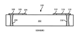
現在の製造技術では、トレース、ビア、および/またはビアパッド同士をどれだけ近くに配置できるかが制限されている。製造技術におけるこのような制限に起因して、ダイおよび基板は、特定の方法で設計する必要がある。図1は、トレース、ビア、および/またはパッドが現在のパッケージ基板にどのように実装されるかを示す。詳細には、図1は、基板102と、いくつかのバンプパッド(たとえば、パッド104、114)と、いくつかのトレース(たとえば、トレース106、116)と、いくつかのビアパッド(たとえば、ビアパッド108、118)とを含むパッケージ基板100の平面図(たとえば、上面図)を示す。バンプパッドは、ダイからのバンプ(たとえば、銅ピラー)に結合するように構成された相互配線である。基板102は、ビアパッドによって覆われているので平面図では見えないいくつかのビアも含む。これらのビアはビアパッドに結合される。図1にさらに示すように、バンプパッド、ビアパッドおよび/またはトレースは、パッケージ基板100においてそれぞれに異なる行および列に沿って配置される。いくつかの実装形態では、パッケージ基板100は、1つまたは複数のダイ(たとえば、フリップチップ)に結合するように構成される。
Current manufacturing techniques limit how close traces, vias, and / or via pads can be placed. Due to these limitations in manufacturing technology, dies and substrates need to be designed in a specific way. FIG. 1 shows how traces, vias, and / or pads are mounted on a current package substrate. Specifically, FIG. 1 illustrates
現在の製造技術では、(たとえば、トレースと比較して)比較的大きいビアパッドが形成され、それによって、ビアは強制的にパッケージ基板のダイ結合領域の外周に向けて形成される。さらに、現在の製造技術は、トレース、ビア、バンプパッド、および/またはビアパッド間のピッチを制限する。製造プロセスにおけるこれらの制限およびその他の制限に起因して、バンプパッド(たとえば、パッド104)がトレース(たとえば、トレース106)を通してビアパッド(たとえば、ビアパッド108)に結合される。この設計によっていくつかの問題が生じる。第一に、この設計では、広い実装面積を占有する集積回路(IC)設計が形成される。第二に、この設計では、余分な相互配線長(たとえば、余分なトレース)によってIC設計の電気的性能が低下することがあるので、性能面の問題が生じる。第三に、追加の相互配線(たとえば、トレース)を付加すると、IC設計がより複雑になる。 Current manufacturing techniques form relatively large via pads (e.g., compared to traces), thereby forcing the vias toward the perimeter of the die bonding region of the package substrate. Furthermore, current manufacturing techniques limit the pitch between traces, vias, bump pads, and / or via pads. Due to these and other limitations in the manufacturing process, a bump pad (eg, pad 104) is coupled to a via pad (eg, via pad 108) through a trace (eg, trace 106). This design creates several problems. First, this design creates an integrated circuit (IC) design that occupies a large mounting area. Second, this design creates performance problems because the extra interconnect length (eg, extra traces) can degrade the electrical performance of the IC design. Third, the addition of additional interconnects (eg, traces) makes IC design more complex.
図2は、図1のパッケージ基板100の断面AAの投影図(たとえば、側面図)を示す。図2に示すように、第1のパッド104(たとえば、バンプパッド)、第1のトレース106、および第2のパッド108(たとえば、ビアパッド)は、基板102の第1の表面上に位置する。パッケージ基板100は、基板102を横断する第1のビア208も含む。第1のパッド104は、第1のトレース106に結合される。第1のトレース106は、第2のパッド108に結合される。第2のパッド108は、第1のビア208に結合される。図2は、第3のパッド114(たとえば、バンプパッド)、第2のトレース116、および第4のパッド118(たとえば、ビアパッド)が、基板102の第1の表面上に位置することも示す。パッケージ基板100は、基板102を横断する第2のビア218も含む。第3のパッド114は、第2のビア116に結合される。第2のビア116は、第4のパッド118に結合される。第4のパッド118は、第2のビア218に結合される。
FIG. 2 shows a projected view (for example, a side view) of the cross section AA of the
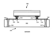
図3は、フリップチップをパッケージ基板にどのように結合することができるかを示す。図3に示すように、第1のバンプ302と第2のバンプ304とを含むフリップチップ300がパッケージ基板100に結合される。第1のバンプ302は、第1のアンダーバンプメタライゼーション(UBM)層と、第1の相互配線ピラー(たとえば、銅ピラー)と、第1のはんだボールとを含んでもよい。第2のバンプ304は、第2のアンダーバンプメタライゼーション(UBM)層と、第2の相互配線ピラー(たとえば、銅ピラー)と、第2のはんだボールとを含んでもよい。フリップチップ300の第1のバンプ302は、第1のパッド104に結合される。フリップチップ300の第2のバンプ304は、第3のパッド114に結合される。図3に示すように、フリップチップ300およびパッケージ基板100の構成では、不必要に大きいパッケージ基板100および/またはフリップチップ300が形成されることがある。たとえば、第1のバンプ302と第1のビア208との間には広い余分な横方向空間/実装面積がある。
FIG. 3 shows how the flip chip can be bonded to the package substrate. As shown in FIG. 3, the
したがって、より小形であり、占有する実装面積がより狭い改良された集積デバイスが必要である。理想的には、そのような集積デバイスは現在の集積デバイスよりも性能が優れている。 Therefore, there is a need for an improved integrated device that is smaller and occupies a smaller footprint. Ideally, such integrated devices perform better than current integrated devices.
本明細書において説明する様々な特徴、装置、および方法は、基板のバンプ領域におけるビアパッドの配置が改良されたパッケージ基板を提供する。 Various features, apparatus, and methods described herein provide a package substrate with improved via pad placement in the bump region of the substrate.
第1の例は、基板と、第1のビアと、第1のバンプパッドとを含む集積デバイスを提供する。第1のビアは基板を横断する。第1のビアは、第1のビア寸法を有する。第1のバンプパッドは、基板の表面上に位置する。第1のバンプパッドは、第1のビアに結合される。第1のバンプパッドは、第1のビア寸法以下の第1のパッド寸法を有する。 The first example provides an integrated device that includes a substrate, a first via, and a first bump pad. The first via traverses the substrate. The first via has a first via dimension. The first bump pad is located on the surface of the substrate. The first bump pad is coupled to the first via. The first bump pad has a first pad dimension that is less than or equal to the first via dimension.
一態様によれば、集積デバイスは、基板を横断する第2のビアを含み、第2のビアは第2のビア寸法を有する。集積デバイスは、基板の表面上に第2のバンプパッドも含み、第2のバンプパッドは第2のビアに結合され、第2のバンプパッドは、第2のビア寸法以下の第2のパッド寸法を有する。いくつかの実装形態では、第1のビアと第2のビアとの間のピッチは約80ミクロン(μm)以下である。いくつかの実装形態では、第1のビアと第2のビアとの間のピッチは約125ミクロン(μm)以下である。 According to one aspect, the integrated device includes a second via that traverses the substrate, the second via having a second via dimension. The integrated device also includes a second bump pad on the surface of the substrate, the second bump pad coupled to the second via, the second bump pad having a second pad dimension less than or equal to the second via dimension. Have In some implementations, the pitch between the first via and the second via is about 80 microns (μm) or less. In some implementations, the pitch between the first via and the second via is about 125 microns (μm) or less.
一態様によれば、第1のバンプパッドは、ダイの相互配線に結合するように構成される。 According to one aspect, the first bump pad is configured to couple to the die interconnect.
一態様によれば、第1のバンプパッドは、基板のダイ領域の縁部の近くに位置する周辺バンプパッドである。 According to one aspect, the first bump pad is a peripheral bump pad located near the edge of the die region of the substrate.
一態様によれば、第1のバンプパッドは、ダイからの第1のバンプに結合するように構成される。いくつかの実装形態では、第1のバンプは、第1のアンダーバンプメタライゼーション(UBM)層と、第1の相互配線ピラーと、第1のはんだボールとを含む。 According to one aspect, the first bump pad is configured to couple to the first bump from the die. In some implementations, the first bump includes a first under bump metallization (UBM) layer, a first interconnect pillar, and a first solder ball.
一態様によれば、基板は、少なくとも誘電体、ガラス、セラミック、および/またはシリコンのうちの1つを含む。 According to one aspect, the substrate comprises at least one of dielectric, glass, ceramic, and / or silicon.
一態様によれば、集積デバイスは、音楽プレーヤ、ビデオプレーヤ、エンターテイメントユニット、ナビゲーションデバイス、通信デバイス、モバイルデバイス、モバイルフォン、スマートフォン、携帯情報端末、固定位置端末、タブレットコンピュータ、および/またはラップトップコンピュータのうちの少なくとも1つに組み込まれる。 According to one aspect, the integrated device is a music player, video player, entertainment unit, navigation device, communication device, mobile device, mobile phone, smartphone, personal digital assistant, fixed location terminal, tablet computer, and / or laptop computer. In at least one of the above.
第2の例は、集積デバイスを作製するための方法を提供する。この方法では、基板を形成する。この方法では、基板を横断する第1のビアを形成し、第1のビアは第1のビア寸法を有する。この方法では、基板の表面上に、第1のビアに結合されるように第1のバンプパッドを形成し、第1のバンプパッドは、第1のビア寸法以下の第1のパッド寸法を有する。 The second example provides a method for making an integrated device. In this method, a substrate is formed. In this method, a first via is formed across the substrate, the first via having a first via dimension. In this method, a first bump pad is formed on a surface of a substrate so as to be coupled to a first via, and the first bump pad has a first pad dimension equal to or smaller than a first via dimension. .
一態様によれば、この方法では、基板を横断する第2のビアをさらに形成し、第2のビアは第2のビア寸法を有する。この方法では、基板の表面上に、第2のビアに結合されるように第2のバンプパッドを形成し、第2のバンプパッドは、第2のビア寸法以下の第2のパッド寸法を有する。いくつかの実装形態では、第1のビアと第2のビアとの間のピッチは約80ミクロン(μm)以下である。いくつかの実装形態では、第1のビアと第2のビアとの間のピッチは約125ミクロン(μm)以下である。 According to one aspect, the method further forms a second via across the substrate, the second via having a second via dimension. In this method, a second bump pad is formed on the surface of the substrate so as to be coupled to the second via, and the second bump pad has a second pad dimension equal to or smaller than the second via dimension. . In some implementations, the pitch between the first via and the second via is about 80 microns (μm) or less. In some implementations, the pitch between the first via and the second via is about 125 microns (μm) or less.
一態様によれば、第1のバンプパッドは、ダイの相互配線に結合するように構成される。 According to one aspect, the first bump pad is configured to couple to the die interconnect.
一態様によれば、第1のバンプパッドは、基板のダイ領域の縁部の近くに位置する周辺バンプパッドである。 According to one aspect, the first bump pad is a peripheral bump pad located near the edge of the die region of the substrate.
一態様によれば、第1のバンプパッドは、ダイからの第1のバンプに結合するように構成される。いくつかの実装形態では、第1のバンプは、第1のアンダーバンプメタライゼーション(UBM)層と、第1の相互配線ピラーと、第1のはんだボールとを含む。 According to one aspect, the first bump pad is configured to couple to the first bump from the die. In some implementations, the first bump includes a first under bump metallization (UBM) layer, a first interconnect pillar, and a first solder ball.
一態様によれば、基板は、少なくとも誘電体、ガラス、セラミック、および/またはシリコンのうちの1つを含む。 According to one aspect, the substrate comprises at least one of dielectric, glass, ceramic, and / or silicon.
一態様によれば、集積デバイスは、音楽プレーヤ、ビデオプレーヤ、エンターテイメントユニット、ナビゲーションデバイス、通信デバイス、モバイルデバイス、モバイルフォン、スマートフォン、携帯情報端末、固定位置端末、タブレットコンピュータ、および/またはラップトップコンピュータのうちの少なくとも1つに組み込まれる。 According to one aspect, the integrated device is a music player, video player, entertainment unit, navigation device, communication device, mobile device, mobile phone, smartphone, personal digital assistant, fixed location terminal, tablet computer, and / or laptop computer. In at least one of the above.
以下に記載される詳細な説明を、同様の参照符号がすべての図面にわたって対応するものを特定する図面とともに検討することによって、種々の特徴、性質、および利点が明らかになろう。 Various features, properties and advantages will become apparent from the detailed description set forth below when considered in conjunction with the drawings, in which like reference characters identify corresponding parts throughout the drawings.
以下の説明では、本開示の様々な態様を完全に理解することが可能なように具体的な詳細を示す。しかしながら、それらの態様が、これらの具体的な詳細なしに実施できることが、当業者には理解されよう。たとえば、態様を不必要に詳しく説明して曖昧にすることを避けるために、回路がブロック図で示される場合がある。他の例では、本開示の態様を曖昧にしないように、周知の回路、構造、および技術は詳細には示されていない場合がある。 In the following description, specific details are set forth to provide a thorough understanding of various aspects of the disclosure. However, those skilled in the art will appreciate that the embodiments can be practiced without these specific details. For example, circuitry may be shown in block diagram form in order to avoid unnecessarily elaborating and obscuring aspects. In other instances, well-known circuits, structures, and techniques may not be shown in detail in order not to obscure aspects of the present disclosure.
(概説)
いくつかの新規の特徴は、基板と、第1のビアと、第1のバンプパッドとを含む集積デバイス(たとえば、半導体デバイス、ダイパッケージ)に関する。第1のビアは基板を横断する。第1のビアは、第1のビア横方向寸法を有する。第1のバンプパッドは、基板の表面上に位置する。第1のバンプパッドは、第1のビアに結合される。第1のバンプパッドは、第1のビア横方向寸法以下の第1のパッド横方向寸法を有する。いくつかの実装形態によれば、第1のバンプパッドは、基板のダイ領域(たとえば、フリップチップ領域)の縁部の近くに位置する周辺バンプパッドである。いくつかの実装形態では、集積デバイスは、第2のビアと第2のバンプパッドとを含む。第2のビアは基板を横断する。第2のビアは、第2のビア横方向寸法を有する。第2のバンプパッドは、基板の表面上に位置する。第2のバンプパッドは、第2のビアに結合される。第2のバンプパッドは、第2のビア横方向寸法以下の第2のパッド横方向寸法を有する。いくつかの実装形態では、第1のビアと第2のビアとの間のピッチは約40ミクロン(μm)以上である。いくつかの実装形態では、第1のビアと第2のビアとの間のピッチは約80ミクロン(μm)以下である。いくつかの実装形態では、第1のビアと第2のビアとの間のピッチは約125ミクロン(μm)以下である。いくつかの実装形態では、第1のバンプパッドと第2のバンプパッドとの間のピッチは約125ミクロン(μm)以下である。いくつかの実装形態では、ピッチは、2つの近隣の相互配線間の中心間距離として定められる。ピッチの例について図8においてさらに説明する。
(Outline)
Some novel features relate to integrated devices (eg, semiconductor devices, die packages) that include a substrate, a first via, and a first bump pad. The first via traverses the substrate. The first via has a first via lateral dimension. The first bump pad is located on the surface of the substrate. The first bump pad is coupled to the first via. The first bump pad has a first pad lateral dimension that is less than or equal to the first via lateral dimension. According to some implementations, the first bump pad is a peripheral bump pad located near the edge of the die region (eg, flip chip region) of the substrate. In some implementations, the integrated device includes a second via and a second bump pad. The second via traverses the substrate. The second via has a second via lateral dimension. The second bump pad is located on the surface of the substrate. The second bump pad is coupled to the second via. The second bump pad has a second pad lateral dimension that is less than or equal to the second via lateral dimension. In some implementations, the pitch between the first and second vias is about 40 microns (μm) or greater. In some implementations, the pitch between the first via and the second via is about 80 microns (μm) or less. In some implementations, the pitch between the first via and the second via is about 125 microns (μm) or less. In some implementations, the pitch between the first bump pad and the second bump pad is about 125 microns (μm) or less. In some implementations, the pitch is defined as the center-to-center distance between two neighboring interconnects. An example of the pitch will be further described with reference to FIG.
(バンプ領域にビアパッドを備える例示的なパッケージ基板)
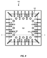
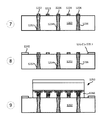
図4は、基板402といくつかの相互配線(たとえば、相互配線408、418)とを含むパッケージ基板400の平面図(たとえば、上面図)を示す。相互配線は、トレース、パッド、および/またはビアを含んでもよい。相互配線408および418は、基板402の第1の表面上に位置するパッドである。いくつかの実装形態では、相互配線408および418はビアパッドおよびバンプパッドである。相互配線408および418は、(たとえば、基板ビアを通して)基板402におけるビアに結合される。これらのビアは、相互配線408および418がビアの断面と同じサイズ(たとえば、同じ横方向寸法)を有するので平面図では見えない。いくつかの実装形態では、相互配線408および418はビアの断面よりも小さい断面を有してもよい。そのような場合、これらのビアは平面図において見えてもよい。ビアの例について図5においてさらに説明する。
(Example package substrate with via pads in bump area)
FIG. 4 shows a plan view (eg, top view) of a
相互配線408および418は、(以下に図6においてさらに説明する)ダイのバンプ(たとえば、相互配線ピラー)に結合するように構成されてもよい。いくつかの実装形態によれば、相互配線408および418は、基板のダイ領域420の縁部の近くに位置する周辺バンプパッドである。いくつかの実装形態では、基板400のダイ領域420は基板400のバンプ領域である。いくつかの実装形態では、基板400のバンプ領域は、ダイが基板に結合されたときにダイが覆うかまたは基板よりも上方に位置する基板の領域である。いくつかの実装形態では、基板のダイ領域の縁部および/または周囲の近くにおいてビアに結合されたビアパッドのサイズを小さくしつつ(たとえば、ビアパッドのピッチを小さくしつつ)基板におけるビアのサイズを維持する。
The
様々な実装態様では、基板402にそれぞれに異なる材料を使用してもよい。いくつかの実装形態では、基板402は、少なくとも誘電体、ガラス、セラミック、および/またはシリコンのうちの1つである。いくつかの実装形態では、パッケージ基板400は、1つまたは複数のダイ(たとえば、フリップチップ)に結合するように構成される。図4は、第1のバンプ領域および第2のバンプ領域も示す。いくつかの実装形態では、バンプ領域は、基板にダイが結合されるときにダイからのバンプ(たとえば、相互配線ピラー)が結合する基板の領域または部分である。いくつかの実装形態では、第1のバンプ領域は相互配線408(たとえば、バンプパッド)の領域に相当する。いくつかの実装形態では、第2のバンプ領域は相互配線418(たとえば、バンプパッド)の領域に相当する。
In various implementations, different materials may be used for the
図4にさらに示すように、相互配線(たとえば、パッド、トレース)は、パッケージ基板400においてそれぞれに異なる行および列に沿って配置される。様々な実装形態では、それぞれに異なる間隔および/またはピッチを相互配線間に使用してもよい。いくつかの実装形態では、2つの近隣の相互配線/隣接する相互配線間のピッチは約125ミクロン(μm)以下である。いくつかの実装形態では、2つの近隣の相互配線/隣接する相互配線間のピッチは約80ミクロン(μm)以下である。いくつかの実装形態では、2つの近隣の相互配線/隣接する相互配線間のピッチは約40ミクロン(μm)以上である。いくつかの実装形態では、ピッチは、2つの隣接する/近隣の相互配線間(たとえば、トレース、ビア、および/またはパッド)の中心間距離として定められる。いくつかの実装形態では、ピッチは、2つの隣接する/近隣のトレース、ビア、および/またはパッド間の中心間距離として定められ、その場合、隣接する/近隣のトレース、ビア、および/またはパッドは、トレース、ビア、および/またはパッドの同じ列内に位置する。いくつかの実装形態では、ピッチは、2つの隣接する/近隣のトレース、ビア、および/またはパッド間の中心間距離として定められ、その場合、隣接する/近隣のトレース、ビア、および/またはパッドは、トレース、ビア、および/またはパッドの同じ行内に位置する。
As further shown in FIG. 4, interconnects (eg, pads, traces) are disposed along different rows and columns, respectively, on
パッケージ基板400の相互配線(たとえば、パッド、トレース)の各々は、少なくとも1つの寸法(たとえば、幅、長さ、直径)を有する。いくつかの実装形態では、トレースの第1の寸法(たとえば、幅)は、ビアの第1の寸法(たとえば、直径)と同じであるかまたはそれよりも小さい。いくつかの実装形態では、パッド(たとえば、ビアパッド、バンプパッド)の第1の寸法(たとえば、幅)は、ビアの第1の寸法(たとえば、直径)と同じであるかまたはそれよりも小さい。
Each interconnect (eg, pad, trace) of
ビアの同じ列に関して、ビアは1行おきに(たとえば、隣接しない行)に位置することに留意されたい。同様に、ビアの同じ行に関して、ビアが1列おきに(たとえば、隣接しない列)に位置することに留意されたい。たとえば、第1の列のビアに関しては、これらのビアは第1の行、第3の行、および/または第5の行に位置する。別の例では、第1の行のビアに関しては、これらのビアは第1の列、第3の列、および/または第5の列に位置する。しかし、ビアは、ビアの隣接する行および/または列に位置してもよい。 Note that for the same column of vias, vias are located every other row (eg, non-adjacent rows). Similarly, note that vias are located in every other column (eg, non-adjacent columns) for the same row of vias. For example, for the first column vias, these vias are located in the first row, the third row, and / or the fifth row. In another example, for the first row of vias, these vias are located in the first column, the third column, and / or the fifth column. However, vias may be located in adjacent rows and / or columns of vias.
ビアパッドの同じ列に関して、ビアパッドが1行おきに(たとえば、隣接しない行)に位置することに留意されたい。同様に、ビアパッドの同じ行に関して、ビアパッドが1列おきに(たとえば、隣接しない列)に位置することに留意されたい。たとえば、第1の列のビアパッドに関しては、これらのビアパッドは第1の行、第3の行、および/または第5の行に位置する。別の例では、第1の行のビアパッドに関しては、これらのビアパッドは第1の列、第3の列、および/または第5の列に位置する。しかし、ビアパッドは、ビアパッドの隣接する行および/または列に位置してもよい。 Note that via pads are located every other row (eg, non-adjacent rows) for the same column of via pads. Similarly, note that via pads are located in every other column (eg, non-adjacent columns) for the same row of via pads. For example, for via pads in the first column, these via pads are located in the first row, the third row, and / or the fifth row. In another example, for the first row of via pads, these via pads are located in the first column, the third column, and / or the fifth column. However, via pads may be located in adjacent rows and / or columns of via pads.
図4に示すように、バンプパッドの少なくともいくつかはビアに直接結合される。したがって、バンプパッドの少なくともいくつかは、ビアに結合されたときにトレースを迂回する。さらに、パッドは、バンプパッドとビアパッドの両方として動作するように構成される。図4は、第1の相互配線408(たとえば、バンプパッド)が直接第1のビア(見えない)に結合されることを示す。同様に、図4は、第2の相互配線418(たとえば、バンプパッド)が直接第2のビア(見えない)に結合されることを示す。第1の相互配線408は、第1のビアに直接結合されたときに、中間トレースを迂回する。同様に、第2の相互配線418は、第2のビアに直接結合されたときに、トレースを迂回する。相互配線とビアとの間の中間トレースを少なくすると、電気的経路が短縮され、それによって集積回路(IC)設計の性能が向上し、かつIC設計の複雑さが低減される。
As shown in FIG. 4, at least some of the bump pads are directly coupled to the vias. Thus, at least some of the bump pads bypass the trace when coupled to the via. Further, the pad is configured to operate as both a bump pad and a via pad. FIG. 4 shows that the first interconnect 408 (eg, bump pad) is coupled directly to the first via (not visible). Similarly, FIG. 4 shows that the second interconnect 418 (eg, bump pad) is coupled directly to the second via (not visible). The
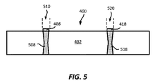
図5は、図4のパッケージ基板400の断面AAの投影図(たとえば、側面図)を示す。図5に示すように、第1の相互配線408および第2の相互配線418は、基板402の第1の表面上に位置する。いくつかの実装形態では、第1の相互配線408および第2の相互配線418は、ダイ(たとえば、フリップチップ)からのバンプ(たとえば、相互配線ピラー)に結合するように構成されたバンプ相互配線(たとえば、バンプパッド)である。図5は、基板402が第1のビア508と第2のビア518とを含むことを示す。第1のビア508および第2のビア518の各々は基板402を横断する。第1の相互配線408は、第1のパッド508に結合される。いくつかの実装形態では、第1の相互配線408のサイズ(たとえば、横方向寸法)は、第1のビア508の断面サイズ(たとえば、横方向寸法)と同じであるかまたはそれによりも小さい。第2の相互配線418は、第2のビア518に直接結合される。いくつかの実装形態では、第2の相互配線418のサイズ(たとえば、横方向寸法)は、第2のビア518の断面サイズ(たとえば、横方向寸法)と同じであるかまたはそれによりも小さい。図5は、第1のバンプ領域510および第2のバンプ領域520も示す。いくつかの実装形態では、第1のバンプ領域510は第1の相互配線408のサイズに相当する。いくつかの実装形態では、第2のバンプ領域520は第2の相互配線418のサイズに相当する。
FIG. 5 shows a projected view (eg, a side view) of section AA of
いくつかの実装形態では、第1のビア508は、第1の金属層と第2の金属層とを含む。いくつかの実装形態では、第1の金属層はシード金属層である。いくつかの実装形態では、第1の金属層は無電解金属層である。いくつかの実装形態では、第2のビア518は、第1の金属層と第2の金属層とを含む。いくつかの実装形態では、第1の金属層はシード金属層である。いくつかの実装形態では、第1の金属層は無電解金属層である。ビア用の第1および第2の金属層の例について図12A〜図12Cにおいて説明する。 In some implementations, the first via 508 includes a first metal layer and a second metal layer. In some implementations, the first metal layer is a seed metal layer. In some implementations, the first metal layer is an electroless metal layer. In some implementations, the second via 518 includes a first metal layer and a second metal layer. In some implementations, the first metal layer is a seed metal layer. In some implementations, the first metal layer is an electroless metal layer. Examples of first and second metal layers for vias are described in FIGS. 12A to 12C.
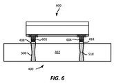
図6は、ダイをパッケージ基板にどのように結合したらよいかを示す。図6に示すように、第1のバンプ602と第2のバンプ604とを含むダイ600(たとえば、フリップチップ、ベアダイ)がパッケージ基板400に結合される。第1のバンプ602は、第1のアンダーバンプメタライゼーション(UBM)層と、第1の相互配線ピラー(たとえば、銅ピラー)と、第1のはんだボールとを含んでもよい。第2のバンプ604は、第2のアンダーバンプメタライゼーション(UBM)層と、第2の相互配線ピラー(たとえば、銅ピラー)と、第2のはんだボールとを含んでもよい。ダイ600の第1のバンプ602は、第1の相互配線408に結合される。ダイ600の第2のバンプ604は、第2の相互配線418に結合される。図6に示すように、第1のバンプ602は、垂直方向において基板402の第1のビア508の上方に(たとえば、部分的に上方に、実質的に上方に、完全に上方に)位置するように第1の相互配線404に結合される。同様に、第2のバンプ604は、垂直方向において基板402の第2のビア518の上方に(たとえば、部分的に上方に、実質的に上方に、完全に上方に)位置するように第2の相互配線418に結合される。いくつかの実装形態では、第1のバンプ602は、第1の相互配線408を横断する電気信号を短絡させずに第1の相互配線408に結合される。いくつかの実装形態では、第2のバンプ604は、第2の相互配線418を横断する電気信号を短絡させずに第2の相互配線418に結合される。
FIG. 6 shows how the die can be bonded to the package substrate. As shown in FIG. 6, a die 600 (eg, flip chip, bare die) including a
図6に示すように、第1のビア508は基板の第1のバンプ領域510に位置する。同様に、第2のビア518は基板の第2のバンプ領域520に位置する。いくつかの実装形態では、バンプ領域は、ダイからのバンプが結合する基板の領域(たとえば、基板の領域または部分)として定められる。第1のバンプ領域510は、ダイ600の第1のバンプ602に結合する第1の相互配線408の部分を含む。いくつかの実装形態では、第1のビア508は、第1のバンプ領域510の下方に位置する。第2のバンプ領域520は、ダイ600の第2のバンプ604に結合する第2の相互配線418の部分を含む。いくつかの実装形態では、第2のビア518は、第2のバンプ領域520の下方に位置する。
As shown in FIG. 6, the first via 508 is located in the first bump region 510 of the substrate. Similarly, the second via 518 is located in the
様々な実装形態は、パッケージ基板におけるビアおよび/またはビアパッドに関してそれぞれに異なる位置および/または構成を有してもよい。 Various implementations may have different locations and / or configurations with respect to vias and / or via pads on the package substrate.
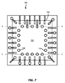
図7は、基板702といくつかの相互配線(たとえば、相互配線708、718)とを含むパッケージ基板700の平面図(上面図)を示す。相互配線は、トレース、パッド、および/またはビアを含んでもよい。相互配線708および718は、基板702の第1の表面上に位置するパッドである。いくつかの実装形態では、相互配線708および718はビアパッドおよびバンプパッドである。相互配線708および718は、(たとえば、基板ビアを通して)基板402におけるビアに結合される。これらのビアは、相互配線708および718がビアの断面と同じサイズを有するので平面図では見えない。いくつかの実装形態では、相互配線708および718はビアの断面よりも小さい断面を有してもよい。そのような場合、これらのビアは平面図において見えてもよい。
FIG. 7 shows a plan view (top view) of a
相互配線708および718は、(以下に図9および図10においてさらに説明する)ダイのバンプ(たとえば、相互配線ピラー)に結合するように構成されてもよい。いくつかの実装形態によれば、相互配線708および718は、基板のダイ領域720の縁部の近くに位置する周辺バンプパッドである。いくつかの実装形態では、基板700のダイ領域720は基板700のバンプ領域である。いくつかの実装形態では、基板700のバンプ領域は、ダイが基板に結合されたときにダイが覆うかまたは基板よりも上方に位置する基板の領域である。いくつかの実装形態では、基板のダイ領域の縁部および/または周囲の近くにおいてビアに結合されたビアパッドのサイズを小さくしつつ(たとえば、ビアパッドのピッチを小さくしつつ)基板におけるビアのサイズを維持する。
様々な実装形態では、基板702にそれぞれに異なる材料を使用してもよい。いくつかの実装形態では、基板層702は、少なくとも誘電体、ガラス、セラミック、および/またはシリコンのうちの1つである。いくつかの実装形態では、パッケージ基板700は、1つまたは複数のダイ(たとえば、フリップチップ)に結合するように構成される。図7は、第1のバンプ領域および第2のバンプ領域も示す。いくつかの実装形態では、バンプ領域は、基板にダイが結合されるときにダイからのバンプ(たとえば、相互配線ピラー)が結合する基板の領域または部分である。いくつかの実装形態では、第1のバンプ領域は相互配線708(たとえば、バンプパッド)の領域に相当する。いくつかの実装形態では、第2のバンプ領域は相互配線718(たとえば、バンプパッド)の領域に相当する。
In various implementations, different materials may be used for the
図7にさらに示すように、相互配線(たとえば、パッド、トレース)は、パッケージ基板700においてそれぞれに異なる行および列に沿って配置される。様々な実装形態では、それぞれに異なる間隔および/またはピッチを相互配線間に使用してもよい。いくつかの実装形態では、2つの近隣の相互配線/隣接する相互配線間のピッチは約125ミクロン(μm)以下である。いくつかの実装形態では、2つの近隣の相互配線/隣接する相互配線間のピッチは約80ミクロン(μm)以下である。いくつかの実装形態では、2つの近隣の相互配線/隣接する相互配線間のピッチは約40ミクロン(μm)以上である。いくつかの実装形態では、ピッチは、2つの隣接する/近隣の相互配線間(たとえば、トレース、ビア、および/またはパッド)の中心間距離として定められる。いくつかの実装形態では、ピッチは、2つの隣接する/近隣のトレース、ビア、および/またはパッド間の中心間距離として定められ、その場合、隣接する/近隣のトレース、ビア、および/またはパッドは、トレース、ビア、および/またはパッドの同じ列内に位置する。いくつかの実装形態では、ピッチは、2つの隣接する/近隣のトレース、ビア、および/またはパッド間の中心間距離として定められ、その場合、隣接する/近隣のトレース、ビア、および/またはパッドは、トレース、ビア、および/またはパッドの同じ行内に位置する。
As further shown in FIG. 7, interconnects (eg, pads, traces) are arranged along different rows and columns, respectively, in
パッケージ基板700の相互配線(たとえば、パッド、トレース)の各々は、少なくとも1つの寸法(たとえば、幅、長さ、直径)を有する。いくつかの実装形態では、トレースの第1の寸法(たとえば、幅)は、ビアの第1の寸法(たとえば、直径)と同じであるかまたはそれよりも小さい。いくつかの実装形態では、パッド(たとえば、ビアパッド、バンプパッド)の第1の寸法(たとえば、幅)は、ビアの第1の寸法(たとえば、直径)と同じであるかまたはそれよりも小さい。
Each interconnect (eg, pad, trace) of
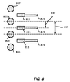
図8は、いくつかの実装形態においてピッチをどのように定めたらよいかを示す。図8は、第1のビアパッド801と、第2のビアパッド803と、第3のビアパッド805と、第4のビアパッド807と、第1のバンプパッド811と、第2のバンプパッド813と、第3のバンプパッド815と、第1の相互配線821と、第2の相互配線823と、第3の相互配線825とを含む基板を示す。図8は、第1のピッチ830および第2のピッチ832も示す。いくつかの実装形態では、第1のピッチ(たとえば、第1のピッチ830)は、それぞれに異なる行または列上の2つの隣接する/近隣の相互配線(たとえば、ビア、トレース、パッド)間の中心間距離である。たとえば、第1のピッチ830は、第3のビアパッド805と第2のバンプパッド813または第2の相互配線823との間の中心間距離であってもよい。いくつかの実装形態では、第1のピッチ830は約40ミクロン(μm)以上であってもよい。
FIG. 8 illustrates how the pitch may be determined in some implementations. FIG. 8 shows a first via
いくつかの実装形態では、第2のピッチ(たとえば、第2のピッチ832)は、同じ行または列上の2つの隣接する/近隣の相互配線(たとえば、ビア、トレース、パッド)間の中心間距離である。たとえば、第2のピッチ832は、第2のビアパッド803と第3のビアパッド805との間の中心間距離であってもよい。別の例では、第2のピッチは、第1のバンプ811と第2のバンプパッド813との間の中心間距離であってもよい。別の例では、第2のピッチは、第2のビアパッド803と第2のバンプパッド813または第2の相互配線823との間の中心間距離であってもよい。別の例では、第1のピッチは、第2の相互配線823と第3の相互配線825との間の中心間距離であってもよい。いくつかの実装形態では、第2のピッチ832は約80ミクロン(μm)以下であってもよい。
In some implementations, the second pitch (eg, second pitch 832) is center-to-center between two adjacent / neighboring interconnects (eg, vias, traces, pads) on the same row or column. Distance. For example, the
様々な実装形態は、トレース、ビア、および/またはビアパッドに関してそれぞれに異なる寸法を有してもよい。たとえば、いくつかの実装形態では、トレースは、幅が約10ミクロン(μm)〜30ミクロン(μm)であってもよい。いくつかの実装形態では、ビアは、幅が約50ミクロン(μm)〜75ミクロン(μm)であってもよい。いくつかの実装形態では、ビアパッドは、幅が約75ミクロン(μm)以下であってもよい。上記の寸法が例にすぎず、本開示におけるトレース、ビア、および/またはビアパッドの寸法を説明における寸法に限定すべきではないことに留意されたい。 Various implementations may have different dimensions with respect to traces, vias, and / or via pads. For example, in some implementations, the trace may be about 10 microns (μm) to 30 microns (μm) wide. In some implementations, the vias may be about 50 microns (μm) to 75 microns (μm) wide. In some implementations, the via pad may be about 75 microns (μm) or less in width. It should be noted that the above dimensions are merely examples, and the dimensions of the traces, vias, and / or via pads in this disclosure should not be limited to the dimensions in the description.
図9は、ダイに結合された図7のパッケージ基板700の断面BBの投影図(たとえば、側面図)を示す。図9に示すように、パッケージ900は、基板902と、ダイ904と、はんだレジスト層906と、アンダーフィル908とを含む。いくつかの実装形態では、ダイ904は、フリップチップおよび/またはベアダイである。
FIG. 9 shows a projected view (eg, side view) of section BB of
パッケージ基板902は、第1のビア910と、第2のビア914と、第3のビア918と、第1の相互配線920と、第2の相互配線924と、第3の相互配線928と、第1のパッド922と、第2のパッド926とを含む。はんだレジスト層906は、基板902の第1の表面に結合される。第1の相互配線920、第2の相互配線924、第3の相互配線928、第1のパッド922、および第2のパッド926は、基板902の第1の表面上に位置する。
The
第1の相互配線920は、第1のビア910に結合される。第1の相互配線920はパッド(たとえば、バンプパッド、ビアパッド)である。第1の相互配線920は、第1のビア910の第1の寸法(たとえば、幅)と同じであるかまたはそれよりも小さい第1の寸法(たとえば、幅)を有する。第2の相互配線924は、第2のビア914に直接結合される。第2の相互配線924はパッド(たとえば、バンプパッド、ビアパッド)である。第2の相互配線924は、第2のビア914の第1の寸法(たとえば、幅)と同じであるかまたはそれよりも小さい第1の寸法(たとえば、幅)を有する。第3の相互配線928は、第3のビア918に結合される。第3の相互配線928はパッド(たとえば、バンプパッド、ビアパッド)である。第3の相互配線928は、第3のビア918の第1の寸法(たとえば、幅)と同じであるかまたはそれよりも小さい第1の寸法(たとえば、幅)を有する。アンダーフィル908は基板902とダイ904との間に位置する。
ダイ904は、第1のバンプ930と、第2のバンプ932と、第3のバンプ934と、第4のバンプ936と、第5のバンプ938とを含む。バンプの各々は、アンダーバンプメタライゼーション(UBM)層と、相互配線ピラー(たとえば、銅ピラー)と、はんだボールとを少なくとも含んでもよい。図9に示すように、第1のバンプ930は、垂直方向において第1のビア910の上方に(たとえば、部分的に上方に、実質的に上方に、完全に上方に)位置するように第1の相互配線920に結合される。第2のバンプ932は、第1のパッド922に結合される。第3のバンプ934は、垂直方向において第2のビア914の上方に(たとえば、部分的に上方に、実質的に上方に、完全に上方に)位置するように第2の相互配線924に結合される。第4のバンプ936は、第2のパッド926に結合される。第5のバンプ938は、垂直方向において第3のビア918の上方に(たとえば、部分的に上方に、実質的に上方に、完全に上方に)位置するように第3の相互配線928に結合される。いくつかの実装形態では、第1のバンプ930は、第1の相互配線920を横断する電気信号を短絡させずに第1の相互配線920に結合される。いくつかの実装形態では、第2のバンプ932は、第2の相互配線922を横断する電気信号を短絡させずに第2の相互配線922に結合される。いくつかの実装形態では、第3のバンプ934は、第3の相互配線924を横断する電気信号を短絡させずに第3の相互配線924に結合される。いくつかの実装形態では、第4のバンプ936は、第4の相互配線926を横断する電気信号を短絡させずに第4の相互配線926に結合される。いくつかの実装形態では、第5のバンプ938は、第5の相互配線928を横断する電気信号を短絡させずに第5の相互配線928に結合される。
The
いくつかの実装形態では、第1のビア910は、第1の金属層と第2の金属層とを含む。いくつかの実装形態では、第1の金属層はシード金属層である。いくつかの実装形態では、第1の金属層は無電解金属層である。いくつかの実装形態では、第2のビア914は、第1の金属層と第2の金属層とを含む。いくつかの実装形態では、第1の金属層はシード金属層である。いくつかの実装形態では、第1の金属層は無電解金属層である。いくつかの実装形態では、第3のビア918は、第1の金属層と第2の金属層とを含む。いくつかの実装形態では、第1の金属層はシード金属層である。いくつかの実装形態では、第1の金属層は無電解金属層である。ビア用の第1および第2の金属層の例について図12A〜図12Cにおいて説明する。 In some implementations, the first via 910 includes a first metal layer and a second metal layer. In some implementations, the first metal layer is a seed metal layer. In some implementations, the first metal layer is an electroless metal layer. In some implementations, the second via 914 includes a first metal layer and a second metal layer. In some implementations, the first metal layer is a seed metal layer. In some implementations, the first metal layer is an electroless metal layer. In some implementations, the third via 918 includes a first metal layer and a second metal layer. In some implementations, the first metal layer is a seed metal layer. In some implementations, the first metal layer is an electroless metal layer. Examples of first and second metal layers for vias are described in FIGS. 12A to 12C.
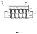
図10は、ダイに結合された図7のパッケージ基板700の断面CCの投影図(たとえば、側面図)を示す。図10に示すように、パッケージ1000は、基板1002と、ダイ1004と、はんだレジスト層1006と、アンダーフィル1008とを含む。いくつかの実装形態では、ダイ1004は、フリップチップおよび/またはベアダイである。
FIG. 10 shows a projected view (eg, a side view) of a cross-section CC of the
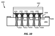
パッケージ基板1002は、第1のビア1010と、第2のビア1012と、第3のビア1014と、第4のビア1016と、第5のビア1018と、第1の相互配線1020と、第2の相互配線1022と、第3の相互配線1024と、第4の相互配線1026と、第5の相互配線1028とを含む。はんだレジスト層1006は、基板1002の第1の表面に結合される。第1の相互配線1020、第2の相互配線1022、第3の相互配線1024、第4の相互配線1026、および第5の相互配線1028は、基板1002の第1の表面上に位置する。
The
第1の相互配線1020は、第1のビア1010に結合される。第1の相互配線1020はパッド(たとえば、バンプパッド、ビアパッド)である。第1の相互配線1020は、第1のビア1010の第1の寸法(たとえば、幅)と同じであるかまたはそれよりも小さい第1の寸法(たとえば、幅)を有する。第2の相互配線1022は、第2のビア1012に結合される。第2の相互配線1022はパッド(たとえば、バンプパッド、ビアパッド)である。第2の相互配線1022は、第2のビア1012の第1の寸法(たとえば、幅)と同じであるかまたはそれよりも小さい第1の寸法(たとえば、幅)を有する。第3の相互配線1024は、第3のビア1014に結合される。第1の相互配線1020はパッド(たとえば、バンプパッド、ビアパッド)である。第3の相互配線1024は、第3のビア1014の第3の寸法(たとえば、幅)と同じであるかまたはそれよりも小さい第1の寸法(たとえば、幅)を有する。第4の相互配線1026は、第4のビア1016に結合される。第4の相互配線1026はパッド(たとえば、バンプパッド、ビアパッド)である。第4の相互配線1026は、第4のビア1016の第1の寸法(たとえば、幅)と同じであるかまたはそれよりも小さい第1の寸法(たとえば、幅)を有する。第5の相互配線1028は、第5のビア1018に結合される。第5の相互配線1028はパッド(たとえば、バンプパッド、ビアパッド)である。第5の相互配線1028は、第5のビア1018の第1の寸法(たとえば、幅)と同じであるかまたはそれよりも小さい第1の寸法(たとえば、幅)を有する。アンダーフィル1008は基板1002とダイ1004との間に位置する。
ダイ1004は、第1のバンプ1030と、第2のバンプ1032と、第3のバンプ1034と、第4のバンプ1036と、第5のバンプ1038とを含む。バンプの各々は、アンダーバンプメタライゼーション(UBM)層と、相互配線ピラー(たとえば、銅ピラー)と、はんだボールとを少なくとも含んでもよい。図10に示すように、第1のバンプ1030は、垂直方向において第1のビア1010の上方に(たとえば、部分的に上方に、実質的に上方に、完全に上方に)位置するように第1の相互配線1020に結合される。第2のバンプ1032は、垂直方向において第2のビア1012の上方に(たとえば、部分的に上方に、実質的に上方に、完全に上方に)位置するように第2の相互配線1022に結合される。第3のバンプ1034は、垂直方向において第3のビア1014の上方に(たとえば、部分的に上方に、実質的に上方に、完全に上方に)位置するように第3の相互配線1024に結合される。第4のバンプ1036は、垂直方向において第4のビア1016の上方に(たとえば、部分的に上方に、実質的に上方に、完全に上方に)位置するように第4の相互配線1026に結合される。第5のバンプ1038は、垂直方向において第5のビア1018の上方に(たとえば、部分的に上方に、実質的に上方に、完全に上方に)位置するように第5の相互配線1028に結合される。
The
いくつかの実装形態では、第1のビア1010は、第1の金属層と第2の金属層とを含む。いくつかの実装形態では、第1の金属層はシード金属層である。いくつかの実装形態では、第1の金属層は無電解金属層である。いくつかの実装形態では、第2のビア1012は、第1の金属層と第2の金属層とを含む。いくつかの実装形態では、第1の金属層はシード金属層である。いくつかの実装形態では、第1の金属層は無電解金属層である。いくつかの実装形態では、第3のビア1014は、第1の金属層と第2の金属層とを含む。いくつかの実装形態では、第1の金属層はシード金属層である。いくつかの実装形態では、第1の金属層は無電解金属層である。ビア用の第1および第2の金属層の例について図12A〜図12Cにおいて説明する。 In some implementations, the first via 1010 includes a first metal layer and a second metal layer. In some implementations, the first metal layer is a seed metal layer. In some implementations, the first metal layer is an electroless metal layer. In some implementations, the second via 1012 includes a first metal layer and a second metal layer. In some implementations, the first metal layer is a seed metal layer. In some implementations, the first metal layer is an electroless metal layer. In some implementations, the third via 1014 includes a first metal layer and a second metal layer. In some implementations, the first metal layer is a seed metal layer. In some implementations, the first metal layer is an electroless metal layer. Examples of first and second metal layers for vias are described in FIGS. 12A to 12C.
図11は、(集積デバイスの形態である)ダイ1100の一例を概念的に示す。いくつかの実装形態では、ダイ1100は、図6のフリップチップ600に相当してもよい。図11に示すように、ダイ1100(たとえば、集積デバイス、ベアダイ)は、基板1101と、いくつかの下位レベル金属層および誘電体層1102と、第1のパッド1104と、第2のパッド1106と、パッシベーション層1108と、第1の絶縁層1110と、第1のアンダーバンプメタライゼーション(UBM)層1112と、第2のアンダーバンプメタライゼーション(UBM)層1114と、第1の相互配線1116(第1のピラー相互配線)と、第2の相互配線1118(たとえば、第2のピラー相互配線)と、第1のはんだ1126と、第2のはんだ1128とを含む。いくつかの実装形態では、第1のUBM層1112、第1の相互配線1116、および第1のはんだボール1126は、総称してダイ1111用の第1のバンプと呼ばれることがある。いくつかの実装形態では、第2のUBM層1114、第2の相互配線1118、および第2のはんだボール1128は、総称してダイ用の第2のバンプと呼ばれることがある。
FIG. 11 conceptually illustrates an example of a die 1100 (in the form of an integrated device). In some implementations, the
バンプ領域の下方にビアを含むいくつかの例示的な基板を提示したが、次に、バンプ領域の下方にビアを含む基板を設ける/製造するためのシーケンスについて以下に説明する。 Having presented several exemplary substrates that include vias below the bump area, a sequence for providing / manufacturing a substrate including vias below the bump area will now be described.
(バンプ領域にビアを含む基板を設けるための例示的なシーケンス)
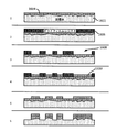
図12(図12A〜図12Cを含む)は、バンプ領域の下方にビアを含む基板を設ける/製造する/作製するための例示的なシーケンスを示す。説明を明快にしかつ簡略化することを目的として、図12A〜図12Cのプロセスが、基板を製造するすべてのステップおよび/または段階を含むとは限らないことに留意されたい。さらに、いくつかの事例では、プロセスの説明を簡単にするために、いくつかのステップおよび/または段階が単一のステップおよび/または段階に結合されている場合がある。図12A〜図12Cのパターンの形状、パターンフィーチャ、構成要素(たとえば、複合材料導電性トレース、ビア)は、概念的な例にすぎず、パターンの実際の形状および形態、パターンフィーチャ、ならびに構成要素を表すとは限らないことにも留意されたい。いくつかの実装形態では、図12A〜図12Cのシーケンスは、本開示において説明する寸法(たとえば、図8において説明した寸法)を有するトレース、ビア、および/またはパッドを作製することができるプロセスを示す。
(Exemplary sequence for providing a substrate including vias in the bump area)
FIG. 12 (including FIGS. 12A-12C) illustrates an exemplary sequence for providing / manufacturing / producing a substrate including a via below a bump region. It should be noted that for purposes of clarity and simplification, the process of FIGS. 12A-12C may not include all steps and / or stages of manufacturing a substrate. Further, in some instances, several steps and / or stages may be combined into a single step and / or stage to simplify the process description. The pattern shapes, pattern features, and components (eg, composite conductive traces, vias) of FIGS. 12A-12C are merely conceptual examples, and the actual shapes and forms of the patterns, pattern features, and components Note also that it does not necessarily represent. In some implementations, the sequence of FIGS. 12A-12C describes a process that can create traces, vias, and / or pads having the dimensions described in this disclosure (eg, the dimensions described in FIG. 8). Show.
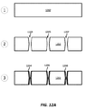
図12Aに示すように、(段階1において)基板(たとえば、基板1202)を設ける。いくつかの実装形態では、基板を設けることは、基板を作製する(たとえば、形成する)ことまたは供給元から基板を受け取ることを含んでもよい。様々な実装形態では、それぞれに異なる材料を基板に使用してもよい。いくつかの実装形態では、基板は、少なくともシリコン、ガラス、セラミック、および/または誘電体のうちの1つを含んでもよい。いくつかの実装形態では、基板はいくつかの層を含んでもよい(たとえば、コア層といくつかのプリプレグ層とを含む積層基板)。 As shown in FIG. 12A, a substrate (eg, substrate 1202) is provided (in stage 1). In some implementations, providing the substrate may include making (eg, forming) the substrate or receiving the substrate from a supplier. In various implementations, different materials may be used for the substrate. In some implementations, the substrate may include at least one of silicon, glass, ceramic, and / or dielectric. In some implementations, the substrate may include several layers (eg, a laminated substrate including a core layer and several prepreg layers).
次に、(段階2において)基板にいくつかのキャビティを設ける。段階2に示すように、基板1202に第1のキャビティ1203、第2のキャビティ1205、および第3のキャビティ1207を設ける。第1のキャビティ1203、第2のキャビティ1205、および第3のキャビティ1207は基板1202を横断する。様々な実装形態は、キャビティを設ける(たとえば、形成する、作製する)ためのそれぞれに異なる製造プロセスを提供してもよい。いくつかの実装形態では、キャビティは、(段階2において)レーザエッチングプロセスを使用して設けられる。
Next, several cavities are provided in the substrate (in stage 2). As shown in
(段階3において)キャビティの壁面に金属層をめっきする。段階3に示すように、第1のキャビティ1203の壁面に第1の金属層1204をめっきし、第2のキャビティ1205の壁面に第2の金属層1206をめっきし、第3のキャビティ1207の壁面に第3の金属層1208をめっきする。いくつかの実装形態では、第1の金属層1204、第2の金属層1206、および第3の金属層1208はシード層(たとえば、無電解金属層)である。いくつかの実装形態では、キャビティの壁上に金属層を設ける(たとえば、形成する、作製する)ことは、無電解銅めっきプロセスを使用することを含む。
(Step 3) Plating a metal layer on the wall of the cavity. As shown in
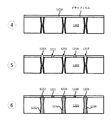
図12Bに示すように、(段階4において)基板(たとえば、基板1202)の第1の表面上にドライフィルム層(たとえば、ドライフィルム1210)を設ける。次に、(段階5において)ドライフィルム層にいくつかの開口部を設ける。段階5に示すように、ドライフィルム層1210に第1の開口部1213、第2の開口部1215、第3の開口部1217、第4の開口部1211、および第5の開口部1219を設ける。様々な実装形態では、それぞれに異なるように開口部を設けても(たとえば、形成しても、作製しても)よい。いくつかの実装形態では、露光および現像技法を使用して開口部を設ける。いくつかの実装形態では、開口部は、基板のキャビティ以下の寸法(たとえば、幅)を有する。
As shown in FIG. 12B, a dry film layer (eg, dry film 1210) is provided (at stage 4) on a first surface of a substrate (eg, substrate 1202). Next (in step 5) several openings are provided in the dry film layer. As shown in
次に、(段階6において)基板にいくつかの金属層を設ける。段階6に示すように、第1のキャビティ1203に金属を充填して第1のビア1232を形成し、第2のキャビティ1205に金属を充填して第2のビア1234を形成し、第3のキャビティ1207に金属を充填して第3のビア1236を形成する。いくつかの実装形態では、第1のビア1232、第2のビア1234、第3のビア1236は、第1の金属層と第2の金属層とを含む。いくつかの実装形態では、ビア(たとえば、ビア1232)の第1の金属はシード層(たとえば、金属層1204)である。いくつかの実装形態では、ビア(たとえば、ビア1234)の第2の金属層は、第1の金属層に結合された銅金属層である。
Next, several metal layers are provided on the substrate (in step 6). As shown in
さらに、第1の開口部1213、第2の開口部1215、第3の開口部1217、第4の開口部1211、および第5の開口部1219に金属を充填してそれぞれ、第1の相互配線1222、第2の相互配線1224、第3の相互配線1226、第4の相互配線1221、および第5の相互配線1229を形成する。いくつかの実装形態では、(段階6において)金属層を設けることは、電気めっきプロセスを使用することを含む。いくつかの実装形態では、相互配線1221、1222、1224、1226、および1229は、ビアの断面サイズと同じであるかまたはそれよりも小さいサイズ(たとえば、横方向寸法)を有する。たとえば、いくつかの実装形態では、相互配線1222のサイズ(たとえば、幅)は、ビア1232の断面サイズ(たとえば、幅)と同じであるかまたはそれによりも小さい。
Further, the
図12Cに示すように、(段階7において)ドライフィルム層(たとえば、ドライフィルム1210)を除去する。いくつかの実装形態では、(段階7において)ドライフィルムを除去することは、エッチングによって残りのドライフィルムを除去することを含む。 As shown in FIG. 12C, the dry film layer (eg, dry film 1210) is removed (in step 7). In some implementations, removing the dry film (in step 7) includes removing the remaining dry film by etching.
(段階8において)基板上にはんだレジスト層(たとえば、はんだレジスト1240)を選択的に設ける。様々な実装形態では、はんだレジスト層を選択的に設けてもよい。いくつかの実装形態では、はんだレジスト層を選択的に設ける(たとえば、形成する、作製する)ことは、はんだレジスト層を設けること、フラッシュエッチングを行うこと、および/またはバックエンド処理を行うことを含む。 (In step 8) A solder resist layer (eg, solder resist 1240) is selectively provided on the substrate. In various implementations, a solder resist layer may be selectively provided. In some implementations, selectively providing (eg, forming, creating) a solder resist layer includes providing a solder resist layer, performing a flash etch, and / or performing a back-end process. Including.
(段階9において)ダイを設けて基板に結合する。いくつかの実装形態では、ダイはフリップチップである。ダイはいくつかのバンプを含む。段階9に示すように、第1のバンプが第1の相互配線に結合されるようにダイを基板に結合する。この場合、第1のバンプは、垂直方向において少なくとも部分的に第1のビアの上方に位置する。段階9は、アンダーフィル1260が基板1202とダイ1250との間に位置することも示す。
(In step 9) A die is provided and bonded to the substrate. In some implementations, the die is a flip chip. The die includes several bumps. As shown in
(バンプ領域にビアパッドを備える例示的なパッケージ基板)
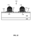
図13は、パッケージ基板の投影図(たとえば、側面図)を示す。図13に示すように、パッケージ1300は、基板1302と、ダイ1304と、はんだレジスト層1306と、アンダーフィル1308とを含む。いくつかの実装形態では、ダイ1304はフリップチップである。
(Example package substrate with via pads in bump area)
FIG. 13 shows a projected view (eg, a side view) of the package substrate. As shown in FIG. 13, the
パッケージ基板1302は、第1のビア1310と、第2のビア1312と、第3のビア1314と、第4のビア1316と、第5のビア1318と、第1の相互配線1320と、第2の相互配線1322と、第3の相互配線1324と、第4の相互配線1326と、第5の相互配線1328とを含む。はんだレジスト層1306は、基板1302の第1の表面に結合される。第1の相互配線1320、第2の相互配線1322、第3の相互配線1324、第4の相互配線1326、および第5の相互配線1328は、基板1302の第1の表面上に位置する。
The
第1の相互配線1320は、第1のビア1310に結合される。第1の相互配線1320はパッド(たとえば、バンプパッド、ビアパッド)である。第1の相互配線1320は、第1のビア1310の第1の寸法(たとえば、幅)と同じであるかまたはそれよりも小さい第1の寸法(たとえば、幅)を有する。第2の相互配線1322は、第2のビア1312に結合される。第2の相互配線1322はパッド(たとえば、バンプパッド、ビアパッド)である。第2の相互配線1322は、第2のビア1312の第1の寸法(たとえば、幅)と同じであるかまたはそれよりも小さい第1の寸法(たとえば、幅)を有する。第3の相互配線1324は、第3のビア1314に結合される。第1の相互配線1320はパッド(たとえば、バンプパッド、ビアパッド)である。第3の相互配線1324は、第3のビア1314の第3の寸法(たとえば、幅)と同じであるかまたはそれよりも小さい第1の寸法(たとえば、幅)を有する。第4の相互配線1326は、第4のビア1316に結合される。第4の相互配線1326はパッド(たとえば、バンプパッド、ビアパッド)である。第4の相互配線1326は、第4のビア1316の第1の寸法(たとえば、幅)と同じであるかまたはそれよりも小さい第1の寸法(たとえば、幅)を有する。第5の相互配線1328は、第5のビア1318に結合される。第5の相互配線1328はパッド(たとえば、バンプパッド、ビアパッド)である。第5の相互配線1328は、第5のビア1318の第1の寸法(たとえば、幅)と同じであるかまたはそれよりも小さい第1の寸法(たとえば、幅)を有する。アンダーフィル1308は基板1302とダイ1304との間に位置する。
ダイ1304は、第1のバンプ1330と、第2のバンプ1332と、第3のバンプ1334と、第4のバンプ1336と、第5のバンプ1338とを含む。バンプの各々は、アンダーバンプメタライゼーション(UBM)層と、相互配線ピラー(たとえば、銅ピラー)と、はんだボールとを少なくとも含んでもよい。図13に示すように、第1のバンプ1330は、垂直方向において第1のビア1310の上方に(たとえば、部分的に上方に、実質的に上方に、完全に上方に)位置するように第1の相互配線1320に結合される。第2のバンプ1332は、垂直方向において第2のビア1312の上方に(たとえば、部分的に上方に、実質的に上方に、完全に上方に)位置するように第2の相互配線1322に結合される。第3のバンプ1334は、垂直方向において第3のビア1314の上方に(たとえば、部分的に上方に、実質的に上方に、完全に上方に)位置するように第3の相互配線1324に結合される。第4のバンプ1336は、垂直方向において第4のビア1316の上方に(たとえば、部分的に上方に、実質的に上方に、完全に上方に)位置するように第4の相互配線1326に結合される。第5のバンプ1338は、垂直方向において第5のビア1318の上方に(たとえば、部分的に上方に、実質的に上方に、完全に上方に)位置するように第5の相互配線1328に結合される。
The
いくつかの実装形態では、第1のビア1310は、第1の金属層1311と第2の金属層1313とを含む。いくつかの実装形態では、第1の金属層1311はシード金属層である。いくつかの実装形態では、第1の金属層1311は無電解金属層である。
In some implementations, the first via 1310 includes a
(バンプ領域にビアを含む基板を設けるための例示的な方法)
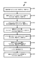
図14は、バンプ領域の下方にビアを含む基板を設ける/製造する/作製するための例示的な方法を示す。説明を明快にしかつ簡略化することを目的として、図14のプロセスが、基板を製造するすべてのステップおよび/または段階を含むとは限らないことに留意されたい。さらに、いくつかの事例では、プロセスの説明を簡単にするために、いくつかのステップおよび/または段階が単一のステップおよび/または段階に結合されている場合がある。図14のパターンの形状、パターンフィーチャ、構成要素(たとえば、複合材料導電性トレース、ビア)は、概念的な例にすぎず、パターンの実際の形状および形態、パターンフィーチャ、ならびに構成要素を表すとは限らないことにも留意されたい。
(Exemplary method for providing a substrate including a via in a bump region)
FIG. 14 illustrates an exemplary method for providing / manufacturing / producing a substrate including vias under a bump region. It should be noted that for purposes of clarity and simplification, the process of FIG. 14 does not include all steps and / or stages of manufacturing a substrate. Further, in some instances, several steps and / or stages may be combined into a single step and / or stage to simplify the process description. The pattern shapes, pattern features, and components (eg, composite conductive traces, vias) in FIG. 14 are merely conceptual examples and represent the actual shape and form of the pattern, pattern features, and components. Note that this is not always the case.
図14に示すように、この方法では、(1405において)基板を設ける。いくつかの実装形態では、(1405において)基板を設けるステップは、基板を作製する(たとえば、形成する)ステップまたは供給元から基板を受け取るステップを含んでもよい。様々な実装形態では、それぞれに異なる材料を基板に使用してもよい。いくつかの実装形態では、基板は、少なくともシリコン、ガラス、セラミック、および/または誘電体のうちの1つを含んでもよい。いくつかの実装形態では、基板はいくつかの層を含んでもよい(たとえば、コア層といくつかのプリプレグ層とを含む積層基板)。 As shown in FIG. 14, the method provides a substrate (at 1405). In some implementations, providing the substrate (at 1405) may include creating (eg, forming) the substrate or receiving the substrate from a supplier. In various implementations, different materials may be used for the substrate. In some implementations, the substrate may include at least one of silicon, glass, ceramic, and / or dielectric. In some implementations, the substrate may include several layers (eg, a laminated substrate including a core layer and several prepreg layers).
次に、この方法では、(1410において)基板に少なくとも1つのキャビティを設ける。たとえば、この方法では、図12Aの段階2に示すように、基板1402に第1のキャビティ1203、第2のキャビティ1205、および第3のキャビティ1207を設ける。第1のキャビティ1403、第2のキャビティ1405、および第3のキャビティ1407は基板1402を横断する。様々な実装形態は、キャビティを設ける(たとえば、形成する、作製する)ためのそれぞれに異なる製造プロセスを提供してもよい。いくつかの実装形態では、キャビティは、(段階1410において)レーザエッチングプロセスを使用して設けられる。
The method then provides (at 1410) at least one cavity in the substrate. For example, in this method, a
この方法では次に(1415において)、少なくとも1つのキャビティの壁上に第1の金属層を設ける。いくつかの実装形態では、第1の金属層を設ける(たとえば、形成する)ステップは、キャビティの壁面を金属層によってめっきするステップを含む。いくつかの実装形態では、第1の金属層は無電解シード金属層である。図12Aの段階3は、第1の金属層を設けるステップの一例を示す。図12Aの段階3に示すように、第1のキャビティ1203の壁面に第1の金属層1204をめっきし、第2のキャビティ1205の壁面に第2の金属層1206をめっきし、第3のキャビティ1207の壁面に第3の金属層1208をめっきする。いくつかの実装形態では、キャビティの壁上に金属層を設ける(たとえば、形成する、作製する)ステップは、無電解銅めっきプロセスを使用するステップを含む。
The method then (at 1415) provides a first metal layer on the walls of at least one cavity. In some implementations, providing (eg, forming) the first metal layer includes plating the walls of the cavity with the metal layer. In some implementations, the first metal layer is an electroless seed metal layer.
この方法では、(1420において)基板上にさらにレジスト層を設ける。いくつかの実装形態では、レジスト層は、ドライフィルム層である。しかしながら、様々な実装態様では、それぞれに異なる材料をレジスト層に使用してもよい。図12Bの段階4は、基板(基板1202)の第1の表面上にドライフィルム層(たとえば、ドライフィルム1210)を設けるステップの一例を示す。
In this method, a resist layer is further provided on the substrate (at 1420). In some implementations, the resist layer is a dry film layer. However, different implementations may use different materials for the resist layer.
この方法では次に、(1425において)レジスト層に少なくとも1つのキャビティ(たとえば、開口部)を設ける。図12Bの段階5は、レジスト層(たとえば、ドライフィルム層)に形成された少なくとも1つのキャビティの一例を示す。段階5に示すように、ドライフィルム層1210に第1の開口部1213、第2の開口部1215、第3の開口部1217、第4の開口部1211、および第5の開口部1219を設ける。様々な実装形態では、それぞれに異なるように開口部を設けても(たとえば、形成しても、作製しても)よい。いくつかの実装形態では、露光および現像技法を使用して開口部を設ける。いくつかの実装形態では、開口部は、基板のキャビティ以下の寸法(たとえば、幅)を有する。
The method then provides (at 1425) at least one cavity (eg, an opening) in the resist layer.
この方法では、(1430において)基板上にさらに第2の金属層を設ける。いくつかの実装形態では、第2の金属層の少なくとも一部は、第1の金属層上に設けられる。図12Bの段階6は、第2の金属層を設けるステップの一例を示す。段階6に示すように、第1のキャビティ1203に金属を充填して第1のビア1232を形成し、第2のキャビティ1205に金属を充填して第2のビア1234を形成し、第3のキャビティ1207に金属を充填して第3のビア1236を形成する。さらに、第1の開口部1213、第2の開口部1215、第3の開口部1217、第4の開口部1211、および第5の開口部1219に金属を充填してそれぞれ、第1の相互配線1222、第2の相互配線1224、第3の相互配線1226、第4の相互配線1221、および第5の相互配線1229を形成する。いくつかの実装形態では、(段階6において)金属層を設けるステップは、電気めっきプロセスを使用するステップを含む。いくつかの実装形態では、相互配線1221、1222、1224、1226、および1229は、ビアの断面サイズと同じであるかまたはそれよりも小さいサイズ(たとえば、横方向寸法)を有する。たとえば、いくつかの実装形態では、相互配線1222のサイズ(たとえば、幅)は、ビア1232の断面サイズ(たとえば、幅)と同じであるかまたはそれによりも小さい。
In this method, a second metal layer is further provided on the substrate (at 1430). In some implementations, at least a portion of the second metal layer is provided on the first metal layer.
この方法では次に、(1435において)レジスト層を除去する。図12Cの段階7は、レジスト層を除去するステップの一例を示す。図12Cの段階7に示すように、ドライフィルム層(たとえば、ドライフィルム1410)を除去する。いくつかの実装形態では、ドライフィルムを除去するステップは、エッチングによって残りのドライフィルムを除去するステップを含む。
The method then removes (at 1435) the resist layer.
この方法ではさらに、(1440において)はんだレジスト層を選択的に設ける。図12Cの段階8は、はんだレジスト層を選択的に設けるステップの一例を示す。図12Cの段階8に示すように、基板上にはんだレジスト層1240を選択的に設ける。様々な実装形態では、はんだレジスト層を選択的に設けてもよい。いくつかの実装形態では、はんだレジスト層を選択的に設ける(たとえば、形成する、作製する)ステップは、はんだレジスト層を設けるステップ、フラッシュエッチングを行うステップ、および/またはバックエンド処理を行うステップを含む。
The method further selectively provides (at 1440) a solder resist layer.
(めっきプロセスのための例示的な流れ図)
図15は、基板を製造するためのモディファイドセミアディティブ法(mSAP)パターニングプロセスの流れ図を示す。図15について、いくつかの実装形態のmSAPプロセス時の基板の層(たとえば、コア層、プリプレグ層)のシーケンスを示す図16を参照しながら説明する。
(Example flow diagram for plating process)
FIG. 15 shows a flow diagram of a modified semi-additive process (mSAP) patterning process for manufacturing a substrate. FIG. 15 will be described with reference to FIG. 16 which shows the sequence of substrate layers (eg, core layer, prepreg layer) during the mSAP process of some implementations.
図15に示すように、プロセス1500は、(1505において)誘電体層上の金属層(たとえば、銅複合材料)を薄膜化することによって開始してもよい。誘電体層は、基板のコア層またはプリプレグ層であり得る。いくつかの実装形態では、金属層は、約3〜5ミクロン(μm)の厚さに薄膜化される。金属層の薄膜化は、薄い銅層1604(銅複合材料であり得る)を含む誘電体層1602を示す、図16の段階1に示される。いくつかの実装形態では、金属層は、すでに十分に薄い場合がある。たとえば、いくつかの実装形態では、コア層または誘電体層は、薄い銅箔を備える場合がある。したがって、いくつかの実装形態では、コア層/誘電体層の金属層の薄膜化をバイパス/スキップしてもよい。加えて、いくつかの実装形態では、無電解銅シード層めっきが、1つまたは複数の誘電体層内の任意のドリリングされたビアの表面を覆うように実行されてもよい。
As shown in FIG. 15,
次に、このプロセスでは、(1510において)ドライフィルムレジスト(DFR)を塗布し、(1515において)DFR上にパターンを作製する。図16の段階2は、DFR1606が薄膜化された金属層1604の頂部上に塗布されることを示し、一方、図16の段階3は、DFR1606のパターニングを示す。段階3に示すように、パターニングによって、DFR1606に開口部1608が形成される。
Next, in this process, a dry film resist (DFR) is applied (at 1510) to create a pattern on the DFR (at 1515).
(1515において)DFRをパターニングした後、次いで、このプロセスでは、(1520において)DFRのパターンを通して銅材料(たとえば、銅複合材料)を電気めっきする。いくつかの実装形態では、電気めっきするステップは、浴溶液内に誘電体および金属層を浸漬するステップを含む。図16を参照すると、段階4は、銅材料(たとえば、銅複合材料)1610がDFR1606の開口部1608にめっきされることを示す。
After patterning the DFR (at 1515), the process then electroplats a copper material (eg, a copper composite) through the DFR pattern (at 1520). In some implementations, electroplating includes immersing the dielectric and metal layers in a bath solution. Referring to FIG. 16,
図15を再び参照すると、このプロセスでは、(1525において)DFRを除去し、(1530において)フィーチャを分離する(たとえば、ビア、複合材料導電性トレース、および/またはパッドなどの構成要素を形成する)ために銅箔材料(たとえば、銅複合材料)を選択的にエッチングし、終了する。図16を参照すると、段階5は、DFR1606の除去を示すが、段階6は、エッチングプロセス後の画定されたフィーチャを示す。図14の上記のプロセスは、基板の各コア層またはプリプレグ層(誘電体層)に関して反復されてもよい。1つのめっきプロセスについて説明してきたが、次に、別のめっきプロセスについて説明する。
Referring again to FIG. 15, the process removes DFR (at 1525) and separates features (at 1530) (eg, forming components such as vias, composite conductive traces, and / or pads). ) Selectively etch copper foil material (eg, copper composite material) and finish. Referring to FIG. 16,
図17は、基板を製造するためのセミアディティブ法(SAP)パターニングプロセスの流れ図である。図17について、いくつかの実装形態のSAPプロセス中の基板の層(たとえば、コア層、プリプレグ層)のシーケンスを示す図18を参照しながら説明する。 FIG. 17 is a flow diagram of a semi-additive process (SAP) patterning process for manufacturing a substrate. FIG. 17 is described with reference to FIG. 18 which shows the sequence of layers (eg, core layer, prepreg layer) of the substrate during the SAP process of some implementations.
図17に示すように、プロセス1700は、(1705において)銅層とプライマ層(たとえば、プライマコーティング銅箔)とを含む誘電体層を設けることによって開始してもよい。いくつかの実装形態では、銅箔は、プライマをコーティングされ、次いで、構造を形成するために未硬化のコア上でプレスされる。プライマコーティング銅箔は、銅箔であってもよい。誘電体層は、基板のコア層またはプリプレグ層であり得る。図18の段階1に示すように、プライマ1804は、銅箔1806と誘電体1802との間に配置される。いくつかの実装形態では、銅箔1806は、銅複合材料箔であってもよい。
As shown in FIG. 17,
次に、このプロセスでは、(1710において)1つまたは複数の開口部/パターンフィーチャ(たとえば、ビアパターンフィーチャ)を形成するために誘電体層(たとえば、コア層、プリプレグ層)をドリリングする。このことは、誘電体の正面と背面とを接続する1つまたは複数のビア/ビアフィーチャを形成するために行われてもよい。いくつかの実装形態では、ドリリングは、レーザドリリング動作によって実行されてもよい。さらに、いくつかの実装形態では、ドリリングは、1つまたは複数の金属層(たとえば、プライマコーティング銅箔)を横断する場合がある。いくつかの実装形態において、このプロセスでは、たとえば、(1712において)層(たとえば、コア層)上のドリリングされたビア/開口部をデスミア処理することによって、ドリリング動作によって形成された開口部/パターンフィーチャ(たとえば、ビアパターン)を清掃する場合もある。 The process then drills (at 1710) a dielectric layer (eg, core layer, prepreg layer) to form one or more opening / pattern features (eg, via pattern features). This may be done to form one or more via / via features that connect the front and back of the dielectric. In some implementations, drilling may be performed by a laser drilling operation. Further, in some implementations, drilling may traverse one or more metal layers (eg, primer coated copper foil). In some implementations, this process includes, for example, opening / pattern formed by a drilling operation by desmearing the drilled via / opening on a layer (eg, core layer) (at 1712). Features (eg, via patterns) may be cleaned.
次いで、このプロセスでは、(1715において)誘電体層上のプライマを残しながら、銅箔をエッチング除去する(これを図18の段階2に示す)。次に、このプロセスでは、いくつかの実装形態において、(1720において)プライマ上に銅シード層(たとえば、銅材料)を無電解めっきする。いくつかの実装形態では、銅シード層の厚さは、約0.1〜1ミクロン(μm)である。図18の段階3は、プライマ1804上の銅シード層1808を示す。
The process then etches away the copper foil (shown in
次に、このプロセスでは、(1725において)ドライフィルムレジスト(DFR)を塗布し、(1730において)DFR上にパターンを形成する。図18の段階4は、DFR1810が銅シード層1808の頂部上に塗布されることを示し、一方、図18の段階5は、DFR1810のパターニングを示す。段階5に示すように、パターニングによって、DFR1810に開口部1812が形成される。
The process then applies a dry film resist (DFR) (at 1725) and forms a pattern on the DFR (at 1730).
(1730において)DFRをパターニングした後、次いで、このプロセスでは、(1735において)DFRのパターンを通して銅材料(たとえば、銅複合材料)を電気めっきする。いくつかの実装形態では、電気めっきするステップは、浴溶液内に誘電体および金属層を浸漬するステップを含む。図18を参照すると、段階6は、銅複合材料1820がDFR1810の開口部1812にめっきされることを示す。
After patterning the DFR (at 1730), the process then electroplats a copper material (eg, a copper composite) through the pattern of DFR (at 1735). In some implementations, electroplating includes immersing the dielectric and metal layers in a bath solution. Referring to FIG. 18,
図17を再び参照すると、このプロセスでは、(1740において)DFRを除去し、(1745において)フィーチャを分離する(たとえば、ビア、トレース、パッドを形成する)ために銅シード層を選択的にエッチングし、終了する。図18を参照すると、段階7は、DFR1810の除去を示し、一方、段階8は、エッチングプロセス後の画定されたフィーチャ(たとえば、複合材料導電性トレース)を示す。
Referring again to FIG. 17, this process selectively etches the copper seed layer to remove DFR (at 1740) and isolate features (eg, form vias, traces, pads) (at 1745). And exit. Referring to FIG. 18,
図17の上記のプロセスは、基板の各コア層またはプリプレグ層(誘電体層)に関して反復されてもよい。 The above process of FIG. 17 may be repeated for each core layer or prepreg layer (dielectric layer) of the substrate.
いくつかの実装形態では、SAPプロセスは、フィーチャを分離するためにそれほどエッチングを必要としないので、より微細な/より小さいフィーチャ(たとえば、トレース、ビア、パッド)の形成を可能にする場合がある。しかし、いくつかの実装形態ではmSAPプロセスの方がSAPプロセスよりもコストが低いことに留意されたい。いくつかの実装形態では、上記のプロセスは、基板にインタースティシャルビアホール(IVH)を形成し並びに/あるいは基板にブラインドビアホール(BVH)を形成するために使用されてもよい。 In some implementations, the SAP process may allow the formation of finer / smaller features (eg, traces, vias, pads) because less etching is required to separate the features. . However, it should be noted that in some implementations, the mSAP process is less expensive than the SAP process. In some implementations, the above process may be used to form interstitial via holes (IVH) in the substrate and / or to form blind via holes (BVH) in the substrate.
いくつかの実装形態では、図15および図17のめっきプロセスは、概念的に図19のめっきプロセスに簡略化されてもよい。図19は、基板を製造するためのめっき法の流れ図を示す。図19に示すように、この方法では、(1905において)基板の層上のドライフィルムレジスト(DFR)内のパターンを通して銅(たとえば、銅複合材料)を電気めっきする。この層は、誘電体層であってもよい。この層は、基板のコア層またはプリプレグ層であってもよい。いくつかの実装形態では、(たとえば、SAPプロセスを使用する際に)この層上に前もって堆積された銅シード層上に、銅(たとえば、銅複合材料)をめっきする。いくつかの実装形態では、(たとえば、mSAPプロセスを使用する際に)この層上に前もって堆積された銅箔層上に、銅(たとえば、銅複合材料)をめっきする。いくつかの実装形態では、銅箔層は、銅複合材料であってもよい。 In some implementations, the plating process of FIGS. 15 and 17 may be conceptually simplified to the plating process of FIG. FIG. 19 shows a flow chart of a plating method for manufacturing a substrate. As shown in FIG. 19, the method electroplats copper (eg, a copper composite) through a pattern in a dry film resist (DFR) on a layer of the substrate (at 1905). This layer may be a dielectric layer. This layer may be the core layer or prepreg layer of the substrate. In some implementations, copper (eg, a copper composite) is plated on a copper seed layer previously deposited on this layer (eg, when using the SAP process). In some implementations, copper (eg, a copper composite) is plated on a copper foil layer previously deposited on this layer (eg, when using an mSAP process). In some implementations, the copper foil layer may be a copper composite material.
次に、この方法では、(1910において)この層からDFRを除去する。いくつかの実装形態では、DFRを除去するステップは、DFRを化学的に除去するステップを含んでもよい。(1910において)DFRを除去した後、この方法では、(1915において)この層のフィーチャを分離/画定するために箔またはシード層を選択的にエッチングし、終了する。上述のように、箔は、銅複合材料であってもよい。 The method then removes the DFR from this layer (at 1910). In some implementations, removing the DFR may include chemically removing the DFR. After removing the DFR (at 1910), the method selectively etches the foil or seed layer (at 1915) to separate / define the features of this layer and ends. As described above, the foil may be a copper composite material.
いくつかの実装形態では、mSAPプロセス(たとえば、図15および図17の方法)時に銅層(たとえば、銅箔)の一部またはすべての上にニッケル合金を付加して(たとえば、めっきして)もよい。同様に、サブトラクティブプロセス時に銅層(たとえば、銅箔)の一部またはすべての上にニッケル合金を付加して(たとえば、めっきして)もよい。 In some implementations, a nickel alloy is added (eg, plated) over some or all of the copper layer (eg, copper foil) during the mSAP process (eg, the method of FIGS. 15 and 17). Also good. Similarly, a nickel alloy may be added (eg, plated) over some or all of the copper layer (eg, copper foil) during the subtractive process.
(例示的な電子デバイス)
図20は、上述の集積デバイス(たとえば、半導体デバイス)、集積回路、ダイ、インターポーザ、および/またはパッケージのうちのいずれかと統合される場合がある様々な電子デバイスを示す。たとえば、モバイル電話2002、ラップトップコンピュータ2004、および固定位置端末2006が、本明細書で説明する集積回路デバイス2000を含んでもよい。集積デバイス2000は、たとえば、本明細書で説明する集積デバイス、集積回路、ダイ、またはパッケージのうちのいずれかであってもよい。図20に示すデバイス2002、2004、2006は例示にすぎない。他の電子デバイスはまた、限定はされないが、モバイルデバイス、ハンドヘルドパーソナル通信システム(PCS)ユニット、携帯情報端末などのポータブルデータユニット、GPS対応デバイス、ナビゲーションデバイス、セットトップボックス、音楽プレーヤ、ビデオプレーヤ、エンターテイメントユニット、メータ読取り機器などの固定位置データユニット、通信デバイス、スマートフォン、タブレットコンピュータ、またはデータもしくはコンピュータ命令を記憶し、もしくは取り出す任意の他のデバイス、またはそれらの任意の組合せを含む、集積デバイス2000を特徴付けてもよい。
(Exemplary electronic device)
FIG. 20 illustrates various electronic devices that may be integrated with any of the integrated devices (eg, semiconductor devices), integrated circuits, dies, interposers, and / or packages described above. For example,
図4、図5、図6、図7、図8、図9、図10、図11、図12A〜図12C、図13、図14、図15、図16、図17、図18、図19、および/または図20に示される構成要素、ステップ、特徴および/または機能のうちの1つまたは複数は、単一の構成要素、ステップ、特徴または機能に再構成されならびに/あるいは組み合わせられてもよく、あるいはいくつかの構成要素、ステップ、または機能として具現化されてもよい。追加の要素、構成要素、ステップ、および/または機能を、本開示から逸脱せずに追加してもよい。 4, 5, 6, 7, 8, 9, 10, 10, 11, 12A to 12C, 13, 14, 15, 16, 17, 17, and 19. And / or one or more of the components, steps, features and / or functions shown in FIG. 20 may be reconfigured and / or combined into a single component, step, feature or function. Or may be embodied as several components, steps, or functions. Additional elements, components, steps, and / or functions may be added without departing from the present disclosure.
「例示的」という言葉は、「例、事例、または例示として役立つ」ことを意味するように本明細書において使用される。「例示的な」として本明細書において説明するいかなる実装形態または態様も、必ずしも本開示の他の態様よりも好ましいか、または有利であると解釈されるべきではない。同様に、「態様」という用語は、本開示のすべての態様が、論じられる特徴、利点、または動作モードを含むことを必要としない。「結合された」という用語は、本明細書において、2つの物体間の直接的または間接的な結合を指すために使用される。たとえば、物体Aが物体Bに物理的に接触し、物体Bが物体Cに接触する場合、物体Aと物体Cとは、互いに物理的に直接接触していなくても、それでも互いに結合するものと見なされてもよい。 The word “exemplary” is used herein to mean “serving as an example, instance, or illustration.” Any implementation or aspect described herein as "exemplary" is not necessarily to be construed as preferred or advantageous over other aspects of the disclosure. Similarly, the term “aspect” does not require that all aspects of the disclosure include the discussed feature, advantage, or mode of operation. The term “coupled” is used herein to refer to a direct or indirect coupling between two objects. For example, when object A physically touches object B and object B touches object C, object A and object C are still in direct contact with each other even if they are not in direct physical contact with each other. May be considered.
また、実施形態については、フローチャート、流れ図、構造図、またはブロック図として示されるプロセスとして説明する場合があることに留意されたい。フローチャートでは動作を順次プロセスとして説明する場合があるが、動作の多くは、並行して実行するかまたは同時に実行することができる。さらに、動作の順序は入れ替えられてもよい。プロセスは、その動作が完了したとき、終了する。 It should also be noted that the embodiments may be described as a process which is depicted as a flowchart, a flow diagram, a structure diagram, or a block diagram. Although a flowchart may describe the operations as a sequential process, many of the operations can be performed in parallel or concurrently. Furthermore, the order of operations may be switched. The process ends when its operation is complete.
本明細書で説明する本開示の様々な特徴は、本開示から逸脱することなく様々なシステムにおいて実現されてもよい。本開示の前述の態様は、例にすぎず、本開示を限定するものとして解釈されるべきではないことに留意されたい。本開示の態様の説明は、例示であることを意図しており、特許請求の範囲を限定することを意図していない。したがって、本教示は、他のタイプの装置に容易に適用することができ、数多くの代替、修正、および変形が、当業者には明らかになるであろう。 Various features of the present disclosure described herein may be implemented in various systems without departing from the disclosure. It should be noted that the foregoing aspects of the disclosure are examples only and should not be construed as limiting the disclosure. The descriptions of aspects of the disclosure are intended to be illustrative and are not intended to limit the scope of the claims. Accordingly, the present teachings can be readily applied to other types of devices and numerous alternatives, modifications, and variations will be apparent to those skilled in the art.
100 パッケージ基板
102 基板
104 第1のパッド
106 第1のトレース
108 第2のパッド
114 第3のパッド
116 第2のトレース
118 第4のパッド
300 フリップチップ
302 第1のバンプ
304 第2のバンプ
400 パッケージ基板
402 基板
404 第1の相互配線
408 相互配線
418 相互配線
420 ダイ領域
510 第1のバンプ領域
520 第2のバンプ領域
600 ダイ
602 第1のバンプ
604 第2のバンプ
700 パッケージ基板
702 基板
708 相互配線
718 相互配線
720 ダイ領域
801 パッド
803 パッド
805 パッド
807 パッド
811 第1のバンプパッド
813 第2のバンプパッド
815 第3のバンプパッド
821 第3の相互配線
823 第2の相互配線
825 第3の相互配線
830 第1のピッチ
832 第2のピッチ
900 パッケージ
902 基板
904 ダイ
906 はんだレジスト層
908 アンダーフィル
920 第1の相互配線
922 第1のパッド
924 第2の相互配線
926 第2のパッド
928 第3の相互配線
930 第1のバンプ
932 第2のバンプ
934 第3のバンプ
936 第4のバンプ
938 第5のバンプ
1000 パッケージ
1002 パッケージ基板
1004 ダイ
1006 はんだレジスト層
1008 アンダーフィル
1020 第1の相互配線
1022 第2の相互配線
1024 第3の相互配線
1026 第4の相互配線
1028 第5の相互配線
1030 第1のバンプ
1032 第2のバンプ
1034 第3のバンプ
1036 第4のバンプ
1038 第5のバンプ
1100 ダイ
1101 基板
1104 第1のパッド
1106 第2のパッド
1108 パッシベーション層
1110 第1の絶縁層
1111 ダイ
1116 第1の相互配線
1118 第2の相互配線
1126 第1のはんだボール
1128 第2のはんだボール
1202 基板
1203 第1のキャビティ
1204 第1の金属層
1205 第2のキャビティ
1206 第2の金属層
1207 第3のキャビティ
1208 第3の金属層
1210 ドライフィルム層
1211 第4の開口部
1213 第1の開口部
1215 第2の開口部
1217 第3の開口部
1219 第5の開口部
1221 第4の相互配線
1222 第1の相互配線
1224 第2の相互配線
1226 第3の相互配線
1229 第5の相互配線
1232 ビア
1240 はんだレジスト層
1250 ダイ
1260 アンダーフィル
1300 パッケージ
1302 基板
1304 ダイ
1306 はんだレジスト層
1308 アンダーフィル
1311 第1の金属層
1313 第2の金属層
1320 第1の相互配線
1322 第2の相互配線
1324 第3の相互配線
1326 第4の相互配線
1328 第5の相互配線
1330 第1のバンプ
1332 第2のバンプ
1334 第3のバンプ
1336 第4のバンプ
1338 第5のバンプ
1402 基板
1403 第1のキャビティ
1405 第2のキャビティ
1407 第3のキャビティ
1602 誘電体層
1604 薄い銅層
1606 DFR
1608 開口部
1802 誘電体
1804 プライマ
1806 銅箔
1808 銅シード層
1810 DFR
1812 開口部
2000 集積デバイス
2002 モバイル電話
2004 ラップトップコンピュータ
2006 固定位置端末
DESCRIPTION OF SYMBOLS 100 Package board | substrate 102 Board | substrate 104 1st pad 106 1st trace 108 2nd pad 114 3rd pad 116 2nd trace 118 4th pad 300 Flip chip 302 1st bump 304 2nd bump 400 Package Substrate 402 Substrate 404 First interconnect 408 Interconnect 418 Interconnect 420 Die region 510 First bump region 520 Second bump region 600 Die 602 First bump 604 Second bump 700 Package substrate 702 Substrate 708 Interconnect 718 Interconnect 720 Die region 801 Pad 803 Pad 805 Pad 807 Pad 811 First bump pad 813 Second bump pad 815 Third bump pad 821 Third interconnect 823 Second interconnect 825 Third interconnect 830 First pitch 832 Second pitch 900 Package 902 Substrate 904 Die 906 Solder resist layer 908 Underfill 920 First interconnect 922 First pad 924 Second interconnect 926 Second pad 928 3rd interconnect 930 1st bump 932 2nd bump 934 3rd bump 936 4th bump 938 5th bump 1000 Package 1002 Package substrate 1004 Die 1006 Solder resist layer 1008 Underfill 1020 1st mutual interconnect Wiring 1022 Second interconnection 1024 Third interconnection 1026 Fourth interconnection 1028 Fifth interconnection 1030 First bump 1032 Second bump 1034 Third bump 1036 Fourth bump 1038 Fifth bump 100 die 1101 substrate 1104 first pad 1106 second pad 1108 passivation layer 1110 first insulating layer 1111 die 1116 first interconnect 1118 second interconnect 1126 first solder ball 1128 second solder ball 1202 Substrate 1203 First cavity 1204 First metal layer 1205 Second cavity 1206 Second metal layer 1207 Third cavity 1208 Third metal layer 1210 Dry film layer 1211 Fourth opening 1213 First opening 1215 2nd opening 1217 3rd opening 1219 5th opening 1221 4th mutual wiring 1222 1st mutual wiring 1224 2nd mutual wiring 1226 3rd mutual wiring 1229 5th mutual wiring 1232 Via 1240 Solder cash register Layer 1250 die 1260 underfill 1300 package 1302 substrate 1304 die 1306 solder resist layer 1308 underfill 1311 first metal layer 1313 second metal layer 1320 first interconnect 1322 second interconnect 1324 third interconnect 1326 4th interconnect 1328 5th interconnect 1330 1st bump 1332 2nd bump 1334 3rd bump 1336 4th bump 1338 5th bump 1402 substrate 1403 1st cavity 1405 2nd cavity 1407 Third cavity 1602 Dielectric layer 1604 Thin copper layer 1606 DFR
1608
1812
Claims (20)
基板と、
前記基板を横断し、第1のビア寸法を有する第1のビアと、
前記基板の表面上に位置し、前記第1のビアに結合され、前記第1のビア寸法以下の第1のパッド寸法を有する第1のバンプパッドとを備える集積デバイス。 An integrated device,
A substrate,
A first via across the substrate and having a first via dimension;
An integrated device comprising: a first bump pad located on a surface of the substrate, coupled to the first via, and having a first pad dimension less than or equal to the first via dimension.
前記基板の前記表面上に位置し、前記第2のビアに結合され、前記第2のビア寸法以下の第2のパッド寸法を有する第2のバンプパッドとをさらに備える、請求項1に記載の集積デバイス。 A second via across the substrate and having a second via dimension;
The second bump pad of claim 1, further comprising a second bump pad positioned on the surface of the substrate, coupled to the second via, and having a second pad dimension less than or equal to the second via dimension. Integrated device.
基板を形成するステップと、
前記基板を横断する第1のビアを形成するステップであって、前記第1のビアは第1のビア寸法を有するステップと、
前記基板の表面上に、前記第1のビアに結合されるように第1のバンプパッドを形成するステップであって、前記第1のバンプパッドは、前記第1のビア寸法以下の第1のパッド寸法を有するステップとを含む方法。 A method for making an integrated device comprising:
Forming a substrate;
Forming a first via across the substrate, the first via having a first via dimension;
Forming a first bump pad on the surface of the substrate so as to be coupled to the first via, the first bump pad having a first via dimension less than or equal to the first via dimension; And a step having a pad dimension.
前記基板の前記表面上に、前記第2のビアに結合されるように第2のバンプパッドを形成するステップであって、前記第2のバンプパッドは、前記第2のビア寸法以下の第2のパッド寸法を有するステップとをさらに含む、請求項11に記載の方法。 Forming a second via across the substrate, the second via having a second via dimension;
Forming a second bump pad on the surface of the substrate so as to be coupled to the second via, the second bump pad being a second smaller than the second via dimension; The method of claim 11, further comprising the step of:
Applications Claiming Priority (5)
| Application Number | Priority Date | Filing Date | Title |
|---|---|---|---|
| US201361919157P | 2013-12-20 | 2013-12-20 | |
| US61/919,157 | 2013-12-20 | ||
| US14/251,518 | 2014-04-11 | ||
| US14/251,518 US9466578B2 (en) | 2013-12-20 | 2014-04-11 | Substrate comprising improved via pad placement in bump area |
| PCT/US2014/070940 WO2015095385A1 (en) | 2013-12-20 | 2014-12-17 | Substrate comprising improved via pad placement in bump area |
Publications (2)
| Publication Number | Publication Date |
|---|---|
| JP2017501575A true JP2017501575A (en) | 2017-01-12 |
| JP2017501575A5 JP2017501575A5 (en) | 2017-03-16 |
Family
ID=53400887
Family Applications (1)
| Application Number | Title | Priority Date | Filing Date |
|---|---|---|---|
| JP2016539908A Pending JP2017501575A (en) | 2013-12-20 | 2014-12-17 | Substrate with improved via pad placement in the bump area |
Country Status (5)
| Country | Link |
|---|---|
| US (1) | US9466578B2 (en) |
| EP (1) | EP3084826A1 (en) |
| JP (1) | JP2017501575A (en) |
| CN (1) | CN105830213B (en) |
| WO (1) | WO2015095385A1 (en) |
Cited By (1)
| Publication number | Priority date | Publication date | Assignee | Title |
|---|---|---|---|---|
| WO2019065656A1 (en) * | 2017-09-29 | 2019-04-04 | 大日本印刷株式会社 | Through-electrode substrate and semiconductor device using through-electrode substrate |
Families Citing this family (4)
| Publication number | Priority date | Publication date | Assignee | Title |
|---|---|---|---|---|
| TWI504320B (en) * | 2014-06-17 | 2015-10-11 | 矽品精密工業股份有限公司 | A circuit structure and fabricating method thereof |
| US9941146B2 (en) * | 2015-07-15 | 2018-04-10 | Chip Solutions, LLC | Semiconductor device and method |
| US10895028B2 (en) | 2015-12-14 | 2021-01-19 | Dupont Industrial Biosciences Usa, Llc | Nonwoven glucan webs |
| JP2017130823A (en) * | 2016-01-21 | 2017-07-27 | 京セラ株式会社 | Piezoelectric oscillator and manufacturing method of the same |
Citations (8)
| Publication number | Priority date | Publication date | Assignee | Title |
|---|---|---|---|---|
| JPH09199535A (en) * | 1996-01-16 | 1997-07-31 | Hitachi Ltd | Electrode structure of semiconductor integrated circuit and its package formation |
| JPH11150158A (en) * | 1997-11-19 | 1999-06-02 | Shinko Electric Ind Co Ltd | Multi layered circuit board |
| US20010008778A1 (en) * | 1999-09-23 | 2001-07-19 | International Business Machines Corporation | Temporary attach article and method for temporary attach of devices to a substrate |
| US20040155347A1 (en) * | 2003-02-07 | 2004-08-12 | Kwun-Yao Ho | Vertical routing structure |
| JP2009135147A (en) * | 2007-11-28 | 2009-06-18 | Shinko Electric Ind Co Ltd | Connection structure of wiring board and electronic element, and electronic device |
| JP2011222901A (en) * | 2010-04-14 | 2011-11-04 | Renesas Electronics Corp | Semiconductor device |
| US20130134581A1 (en) * | 2011-11-30 | 2013-05-30 | Taiwan Semiconductor Manufacturing Company, Ltd. | Planarized bumps for underfill control |
| US20130264720A1 (en) * | 2012-04-09 | 2013-10-10 | Samsung Electronics Co., Ltd. | Semiconductor Chips Having Through Silicon Vias and Related Fabrication Methods and Semiconductor Packages |
Family Cites Families (14)
| Publication number | Priority date | Publication date | Assignee | Title |
|---|---|---|---|---|
| EP0851724B1 (en) | 1996-12-26 | 2003-10-22 | Matsushita Electric Industrial Co., Ltd. | Printed circuit board and electric components |
| JP3386977B2 (en) | 1997-06-05 | 2003-03-17 | 新光電気工業株式会社 | Multilayer circuit board |
| US6940176B2 (en) | 2002-05-21 | 2005-09-06 | United Microelectronics Corp. | Solder pads for improving reliability of a package |
| WO2004047167A1 (en) | 2002-11-21 | 2004-06-03 | Nec Corporation | Semiconductor device, wiring substrate, and method for manufacturing wiring substrate |
| JP3986989B2 (en) * | 2003-03-27 | 2007-10-03 | 松下電器産業株式会社 | Semiconductor device |
| US7939941B2 (en) | 2007-06-27 | 2011-05-10 | Taiwan Semiconductor Manufacturing Company, Ltd. | Formation of through via before contact processing |
| WO2009048154A1 (en) | 2007-10-12 | 2009-04-16 | Nec Corporation | Semiconductor device and method for designing the same |
| JP2009260098A (en) | 2008-04-18 | 2009-11-05 | Shinko Electric Ind Co Ltd | Wiring substrate, and semiconductor device |
| US8227295B2 (en) | 2008-10-16 | 2012-07-24 | Texas Instruments Incorporated | IC die having TSV and wafer level underfill and stacked IC devices comprising a workpiece solder connected to the TSV |
| US8344503B2 (en) * | 2008-11-25 | 2013-01-01 | Freescale Semiconductor, Inc. | 3-D circuits with integrated passive devices |
| TWI420643B (en) | 2008-12-16 | 2013-12-21 | Powertech Technology Inc | Chip having tsv's, its forming method and a chip stack utilizing the chip |
| US8791549B2 (en) * | 2009-09-22 | 2014-07-29 | Taiwan Semiconductor Manufacturing Company, Ltd. | Wafer backside interconnect structure connected to TSVs |
| US9167694B2 (en) | 2010-11-02 | 2015-10-20 | Georgia Tech Research Corporation | Ultra-thin interposer assemblies with through vias |
| GB2485830A (en) * | 2010-11-26 | 2012-05-30 | Cambridge Silicon Radio Ltd | Stacked multi-chip package using encapsulated electroplated pillar conductors; also able to include MEMS elements |
-
2014
- 2014-04-11 US US14/251,518 patent/US9466578B2/en not_active Expired - Fee Related
- 2014-12-17 CN CN201480069410.XA patent/CN105830213B/en not_active Expired - Fee Related
- 2014-12-17 JP JP2016539908A patent/JP2017501575A/en active Pending
- 2014-12-17 WO PCT/US2014/070940 patent/WO2015095385A1/en active Application Filing
- 2014-12-17 EP EP14825040.0A patent/EP3084826A1/en not_active Withdrawn
Patent Citations (8)
| Publication number | Priority date | Publication date | Assignee | Title |
|---|---|---|---|---|
| JPH09199535A (en) * | 1996-01-16 | 1997-07-31 | Hitachi Ltd | Electrode structure of semiconductor integrated circuit and its package formation |
| JPH11150158A (en) * | 1997-11-19 | 1999-06-02 | Shinko Electric Ind Co Ltd | Multi layered circuit board |
| US20010008778A1 (en) * | 1999-09-23 | 2001-07-19 | International Business Machines Corporation | Temporary attach article and method for temporary attach of devices to a substrate |
| US20040155347A1 (en) * | 2003-02-07 | 2004-08-12 | Kwun-Yao Ho | Vertical routing structure |
| JP2009135147A (en) * | 2007-11-28 | 2009-06-18 | Shinko Electric Ind Co Ltd | Connection structure of wiring board and electronic element, and electronic device |
| JP2011222901A (en) * | 2010-04-14 | 2011-11-04 | Renesas Electronics Corp | Semiconductor device |
| US20130134581A1 (en) * | 2011-11-30 | 2013-05-30 | Taiwan Semiconductor Manufacturing Company, Ltd. | Planarized bumps for underfill control |
| US20130264720A1 (en) * | 2012-04-09 | 2013-10-10 | Samsung Electronics Co., Ltd. | Semiconductor Chips Having Through Silicon Vias and Related Fabrication Methods and Semiconductor Packages |
Cited By (3)
| Publication number | Priority date | Publication date | Assignee | Title |
|---|---|---|---|---|
| WO2019065656A1 (en) * | 2017-09-29 | 2019-04-04 | 大日本印刷株式会社 | Through-electrode substrate and semiconductor device using through-electrode substrate |
| JPWO2019065656A1 (en) * | 2017-09-29 | 2020-11-19 | 大日本印刷株式会社 | Through silicon via substrate and semiconductor device using through silicon via substrate |
| JP7180605B2 (en) | 2017-09-29 | 2022-11-30 | 大日本印刷株式会社 | Through electrode substrate and semiconductor device using through electrode substrate |
Also Published As
| Publication number | Publication date |
|---|---|
| EP3084826A1 (en) | 2016-10-26 |
| CN105830213B (en) | 2019-09-10 |
| WO2015095385A1 (en) | 2015-06-25 |
| CN105830213A (en) | 2016-08-03 |
| US9466578B2 (en) | 2016-10-11 |
| US20150179590A1 (en) | 2015-06-25 |
Similar Documents
| Publication | Publication Date | Title |
|---|---|---|
| US11443970B2 (en) | Methods of forming a package substrate | |
| JP6240342B2 (en) | Package substrate with surface interconnections and cavities containing electroless fill | |
| KR20180044905A (en) | An integrated device package including bridges in a litho-etchable layer | |
| US9368566B2 (en) | Package on package (PoP) integrated device comprising a capacitor in a substrate | |
| CN107004612B (en) | Integrated device package including photosensitive filler between substrate and die | |
| KR102428876B1 (en) | A method and package for manufacturing a package substrate. | |
| KR101255954B1 (en) | Printed circuit board and manufacturing method thereof | |
| US10651160B2 (en) | Low profile integrated package | |
| JP2017501575A (en) | Substrate with improved via pad placement in the bump area | |
| TW202017135A (en) | High density interconnects in an embedded trace substrate (ets) comprising a core layer | |
| US9355898B2 (en) | Package on package (PoP) integrated device comprising a plurality of solder resist layers | |
| US20160183379A1 (en) | Substrate comprising an embedded capacitor | |
| US20160316557A1 (en) | Printed circuit board, manufacturing method thereof and electronic component module | |
| CN104392937A (en) | Method to increase i/o density and reduce layer counts in bbul packages | |
| US9807884B2 (en) | Substrate comprising embedded elongated capacitor | |
| US20160198568A1 (en) | Printed circuit board and electronic component module | |
| TW201921590A (en) | Fine pitch and spacing interconnects with reserve interconnect portion | |
| US10157824B2 (en) | Integrated circuit (IC) package and package substrate comprising stacked vias | |
| JP2008305952A (en) | High density fine line mounting structure and manufacturing method of the same |
Legal Events
| Date | Code | Title | Description |
|---|---|---|---|
| A521 | Request for written amendment filed |
Free format text: JAPANESE INTERMEDIATE CODE: A523 Effective date: 20160621 |
|
| A521 | Request for written amendment filed |
Free format text: JAPANESE INTERMEDIATE CODE: A523 Effective date: 20170209 |
|
| A621 | Written request for application examination |
Free format text: JAPANESE INTERMEDIATE CODE: A621 Effective date: 20170209 |
|
| A871 | Explanation of circumstances concerning accelerated examination |
Free format text: JAPANESE INTERMEDIATE CODE: A871 Effective date: 20170209 |
|
| A975 | Report on accelerated examination |
Free format text: JAPANESE INTERMEDIATE CODE: A971005 Effective date: 20170215 |
|
| A131 | Notification of reasons for refusal |
Free format text: JAPANESE INTERMEDIATE CODE: A131 Effective date: 20170306 |
|
| A601 | Written request for extension of time |
Free format text: JAPANESE INTERMEDIATE CODE: A601 Effective date: 20170606 |
|
| A02 | Decision of refusal |
Free format text: JAPANESE INTERMEDIATE CODE: A02 Effective date: 20171120 |