JP2017143679A - パワーモジュール - Google Patents
パワーモジュール Download PDFInfo
- Publication number
- JP2017143679A JP2017143679A JP2016024419A JP2016024419A JP2017143679A JP 2017143679 A JP2017143679 A JP 2017143679A JP 2016024419 A JP2016024419 A JP 2016024419A JP 2016024419 A JP2016024419 A JP 2016024419A JP 2017143679 A JP2017143679 A JP 2017143679A
- Authority
- JP
- Japan
- Prior art keywords
- lead
- power module
- package
- connection point
- module according
- Prior art date
- Legal status (The legal status is an assumption and is not a legal conclusion. Google has not performed a legal analysis and makes no representation as to the accuracy of the status listed.)
- Pending
Links
Images


Classifications
-
- H—ELECTRICITY
- H02—GENERATION; CONVERSION OR DISTRIBUTION OF ELECTRIC POWER
- H02M—APPARATUS FOR CONVERSION BETWEEN AC AND AC, BETWEEN AC AND DC, OR BETWEEN DC AND DC, AND FOR USE WITH MAINS OR SIMILAR POWER SUPPLY SYSTEMS; CONVERSION OF DC OR AC INPUT POWER INTO SURGE OUTPUT POWER; CONTROL OR REGULATION THEREOF
- H02M1/00—Details of apparatus for conversion
- H02M1/32—Means for protecting converters other than automatic disconnection
- H02M1/34—Snubber circuits
-
- H—ELECTRICITY
- H02—GENERATION; CONVERSION OR DISTRIBUTION OF ELECTRIC POWER
- H02M—APPARATUS FOR CONVERSION BETWEEN AC AND AC, BETWEEN AC AND DC, OR BETWEEN DC AND DC, AND FOR USE WITH MAINS OR SIMILAR POWER SUPPLY SYSTEMS; CONVERSION OF DC OR AC INPUT POWER INTO SURGE OUTPUT POWER; CONTROL OR REGULATION THEREOF
- H02M7/00—Conversion of ac power input into dc power output; Conversion of dc power input into ac power output
- H02M7/42—Conversion of dc power input into ac power output without possibility of reversal
- H02M7/44—Conversion of dc power input into ac power output without possibility of reversal by static converters
- H02M7/48—Conversion of dc power input into ac power output without possibility of reversal by static converters using discharge tubes with control electrode or semiconductor devices with control electrode
-
- H—ELECTRICITY
- H01—ELECTRIC ELEMENTS
- H01L—SEMICONDUCTOR DEVICES NOT COVERED BY CLASS H10
- H01L23/00—Details of semiconductor or other solid state devices
- H01L23/48—Arrangements for conducting electric current to or from the solid state body in operation, e.g. leads, terminal arrangements ; Selection of materials therefor
- H01L23/488—Arrangements for conducting electric current to or from the solid state body in operation, e.g. leads, terminal arrangements ; Selection of materials therefor consisting of soldered or bonded constructions
- H01L23/495—Lead-frames or other flat leads
- H01L23/49589—Capacitor integral with or on the leadframe
-
- H—ELECTRICITY
- H01—ELECTRIC ELEMENTS
- H01L—SEMICONDUCTOR DEVICES NOT COVERED BY CLASS H10
- H01L23/00—Details of semiconductor or other solid state devices
- H01L23/48—Arrangements for conducting electric current to or from the solid state body in operation, e.g. leads, terminal arrangements ; Selection of materials therefor
- H01L23/488—Arrangements for conducting electric current to or from the solid state body in operation, e.g. leads, terminal arrangements ; Selection of materials therefor consisting of soldered or bonded constructions
- H01L23/498—Leads, i.e. metallisations or lead-frames on insulating substrates, e.g. chip carriers
- H01L23/49838—Geometry or layout
- H01L23/49844—Geometry or layout for devices being provided for in H01L29/00
-
- H—ELECTRICITY
- H01—ELECTRIC ELEMENTS
- H01L—SEMICONDUCTOR DEVICES NOT COVERED BY CLASS H10
- H01L23/00—Details of semiconductor or other solid state devices
- H01L23/48—Arrangements for conducting electric current to or from the solid state body in operation, e.g. leads, terminal arrangements ; Selection of materials therefor
- H01L23/488—Arrangements for conducting electric current to or from the solid state body in operation, e.g. leads, terminal arrangements ; Selection of materials therefor consisting of soldered or bonded constructions
- H01L23/498—Leads, i.e. metallisations or lead-frames on insulating substrates, e.g. chip carriers
- H01L23/49861—Lead-frames fixed on or encapsulated in insulating substrates
-
- H—ELECTRICITY
- H01—ELECTRIC ELEMENTS
- H01L—SEMICONDUCTOR DEVICES NOT COVERED BY CLASS H10
- H01L25/00—Assemblies consisting of a plurality of individual semiconductor or other solid state devices ; Multistep manufacturing processes thereof
- H01L25/03—Assemblies consisting of a plurality of individual semiconductor or other solid state devices ; Multistep manufacturing processes thereof all the devices being of a type provided for in the same subgroup of groups H01L27/00 - H01L33/00, or in a single subclass of H10K, H10N, e.g. assemblies of rectifier diodes
- H01L25/04—Assemblies consisting of a plurality of individual semiconductor or other solid state devices ; Multistep manufacturing processes thereof all the devices being of a type provided for in the same subgroup of groups H01L27/00 - H01L33/00, or in a single subclass of H10K, H10N, e.g. assemblies of rectifier diodes the devices not having separate containers
- H01L25/07—Assemblies consisting of a plurality of individual semiconductor or other solid state devices ; Multistep manufacturing processes thereof all the devices being of a type provided for in the same subgroup of groups H01L27/00 - H01L33/00, or in a single subclass of H10K, H10N, e.g. assemblies of rectifier diodes the devices not having separate containers the devices being of a type provided for in group H01L29/00
- H01L25/072—Assemblies consisting of a plurality of individual semiconductor or other solid state devices ; Multistep manufacturing processes thereof all the devices being of a type provided for in the same subgroup of groups H01L27/00 - H01L33/00, or in a single subclass of H10K, H10N, e.g. assemblies of rectifier diodes the devices not having separate containers the devices being of a type provided for in group H01L29/00 the devices being arranged next to each other
-
- H—ELECTRICITY
- H01—ELECTRIC ELEMENTS
- H01L—SEMICONDUCTOR DEVICES NOT COVERED BY CLASS H10
- H01L25/00—Assemblies consisting of a plurality of individual semiconductor or other solid state devices ; Multistep manufacturing processes thereof
- H01L25/18—Assemblies consisting of a plurality of individual semiconductor or other solid state devices ; Multistep manufacturing processes thereof the devices being of types provided for in two or more different subgroups of the same main group of groups H01L27/00 - H01L33/00, or in a single subclass of H10K, H10N
-
- H—ELECTRICITY
- H02—GENERATION; CONVERSION OR DISTRIBUTION OF ELECTRIC POWER
- H02H—EMERGENCY PROTECTIVE CIRCUIT ARRANGEMENTS
- H02H3/00—Emergency protective circuit arrangements for automatic disconnection directly responsive to an undesired change from normal electric working condition with or without subsequent reconnection ; integrated protection
- H02H3/20—Emergency protective circuit arrangements for automatic disconnection directly responsive to an undesired change from normal electric working condition with or without subsequent reconnection ; integrated protection responsive to excess voltage
-
- H—ELECTRICITY
- H02—GENERATION; CONVERSION OR DISTRIBUTION OF ELECTRIC POWER
- H02M—APPARATUS FOR CONVERSION BETWEEN AC AND AC, BETWEEN AC AND DC, OR BETWEEN DC AND DC, AND FOR USE WITH MAINS OR SIMILAR POWER SUPPLY SYSTEMS; CONVERSION OF DC OR AC INPUT POWER INTO SURGE OUTPUT POWER; CONTROL OR REGULATION THEREOF
- H02M7/00—Conversion of ac power input into dc power output; Conversion of dc power input into ac power output
- H02M7/003—Constructional details, e.g. physical layout, assembly, wiring or busbar connections
-
- H—ELECTRICITY
- H02—GENERATION; CONVERSION OR DISTRIBUTION OF ELECTRIC POWER
- H02M—APPARATUS FOR CONVERSION BETWEEN AC AND AC, BETWEEN AC AND DC, OR BETWEEN DC AND DC, AND FOR USE WITH MAINS OR SIMILAR POWER SUPPLY SYSTEMS; CONVERSION OF DC OR AC INPUT POWER INTO SURGE OUTPUT POWER; CONTROL OR REGULATION THEREOF
- H02M7/00—Conversion of ac power input into dc power output; Conversion of dc power input into ac power output
- H02M7/42—Conversion of dc power input into ac power output without possibility of reversal
- H02M7/44—Conversion of dc power input into ac power output without possibility of reversal by static converters
- H02M7/48—Conversion of dc power input into ac power output without possibility of reversal by static converters using discharge tubes with control electrode or semiconductor devices with control electrode
- H02M7/53—Conversion of dc power input into ac power output without possibility of reversal by static converters using discharge tubes with control electrode or semiconductor devices with control electrode using devices of a triode or transistor type requiring continuous application of a control signal
- H02M7/537—Conversion of dc power input into ac power output without possibility of reversal by static converters using discharge tubes with control electrode or semiconductor devices with control electrode using devices of a triode or transistor type requiring continuous application of a control signal using semiconductor devices only, e.g. single switched pulse inverters
- H02M7/5387—Conversion of dc power input into ac power output without possibility of reversal by static converters using discharge tubes with control electrode or semiconductor devices with control electrode using devices of a triode or transistor type requiring continuous application of a control signal using semiconductor devices only, e.g. single switched pulse inverters in a bridge configuration
-
- H—ELECTRICITY
- H02—GENERATION; CONVERSION OR DISTRIBUTION OF ELECTRIC POWER
- H02M—APPARATUS FOR CONVERSION BETWEEN AC AND AC, BETWEEN AC AND DC, OR BETWEEN DC AND DC, AND FOR USE WITH MAINS OR SIMILAR POWER SUPPLY SYSTEMS; CONVERSION OF DC OR AC INPUT POWER INTO SURGE OUTPUT POWER; CONTROL OR REGULATION THEREOF
- H02M1/00—Details of apparatus for conversion
- H02M1/32—Means for protecting converters other than automatic disconnection
- H02M1/34—Snubber circuits
- H02M1/346—Passive non-dissipative snubbers
-
- H—ELECTRICITY
- H02—GENERATION; CONVERSION OR DISTRIBUTION OF ELECTRIC POWER
- H02M—APPARATUS FOR CONVERSION BETWEEN AC AND AC, BETWEEN AC AND DC, OR BETWEEN DC AND DC, AND FOR USE WITH MAINS OR SIMILAR POWER SUPPLY SYSTEMS; CONVERSION OF DC OR AC INPUT POWER INTO SURGE OUTPUT POWER; CONTROL OR REGULATION THEREOF
- H02M1/00—Details of apparatus for conversion
- H02M1/32—Means for protecting converters other than automatic disconnection
- H02M1/34—Snubber circuits
- H02M1/348—Passive dissipative snubbers
-
- Y—GENERAL TAGGING OF NEW TECHNOLOGICAL DEVELOPMENTS; GENERAL TAGGING OF CROSS-SECTIONAL TECHNOLOGIES SPANNING OVER SEVERAL SECTIONS OF THE IPC; TECHNICAL SUBJECTS COVERED BY FORMER USPC CROSS-REFERENCE ART COLLECTIONS [XRACs] AND DIGESTS
- Y02—TECHNOLOGIES OR APPLICATIONS FOR MITIGATION OR ADAPTATION AGAINST CLIMATE CHANGE
- Y02B—CLIMATE CHANGE MITIGATION TECHNOLOGIES RELATED TO BUILDINGS, e.g. HOUSING, HOUSE APPLIANCES OR RELATED END-USER APPLICATIONS
- Y02B70/00—Technologies for an efficient end-user side electric power management and consumption
- Y02B70/10—Technologies improving the efficiency by using switched-mode power supplies [SMPS], i.e. efficient power electronics conversion e.g. power factor correction or reduction of losses in power supplies or efficient standby modes
Abstract
【解決手段】パワーモジュールは、一端が第1接続点2aに電気的に接続され、他端がパッケージ1から露出された、第1リード4aよりも短い第3リード7aと、一端が第2接続点2bに電気的に接続され、他端がパッケージ1から露出された、第2リード4bよりも短い第4リード7bとを備える。第3リード7aの他端及び第4リード7bの他端に、スナバコンデンサ6が着脱可能である。
【選択図】図2
Description
まず、本発明の実施の形態に係るパワーモジュールについて説明する前に、これと関連するパワーモジュール(以下、「関連パワーモジュール」と記す)について説明する。
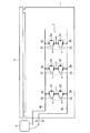
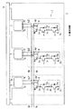
図2は、本実施の形態1に係るパワーモジュールの構成を示す断面図である。なお、本実施の形態1で説明する構成要素のうち、関連パワーモジュールと同じまたは類似する構成要素については同じ参照符号を付し、異なる構成要素について主に説明する。
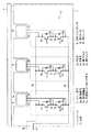
図3は、本実施の形態2に係るパワーモジュールの構成を示す断面図である。なお、本実施の形態2で説明する構成要素のうち、実施の形態1と同じまたは類似する構成要素については同じ参照符号を付し、異なる構成要素について主に説明する。
図4は、本実施の形態3に係るパワーモジュールの構成を示す断面図である。なお、本実施の形態3で説明する構成要素のうち、実施の形態1と同じまたは類似する構成要素については同じ参照符号を付し、異なる構成要素について主に説明する。
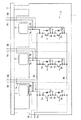
図5は、本実施の形態4に係るパワーモジュールの構成を示す断面図である。なお、本実施の形態4で説明する構成要素のうち、実施の形態2,3と同じまたは類似する構成要素については同じ参照符号を付し、異なる構成要素について主に説明する。
図6は、本実施の形態5に係るパワーモジュールの構成を示す断面図である。なお、本実施の形態5で説明する構成要素のうち、実施の形態1と同じまたは類似する構成要素については同じ参照符号を付し、異なる構成要素について主に説明する。
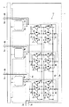
図7は、本実施の形態6に係るパワーモジュールの構成を示す断面図である。なお、本実施の形態6で説明する構成要素のうち、実施の形態3,5と同じまたは類似する構成要素については同じ参照符号を付し、異なる構成要素について主に説明する。
図8は、本実施の形態7に係るパワーモジュールの構成を示す断面図である。なお、本実施の形態7で説明する構成要素のうち、実施の形態1と同じまたは類似する構成要素については同じ参照符号を付し、異なる構成要素について主に説明する。
図9は、本実施の形態8に係るパワーモジュールの構成を示す断面図である。なお、本実施の形態8で説明する構成要素のうち、実施の形態3,7と同じまたは類似する構成要素については同じ参照符号を付し、異なる構成要素について主に説明する。
図10は、本実施の形態9に係るパワーモジュールの構成を示す断面図である。なお、本実施の形態9で説明する構成要素のうち、実施の形態1と同じまたは類似する構成要素については同じ参照符号を付し、異なる構成要素について主に説明する。
Claims (11)
- パッケージと、
前記パッケージ内に設けられ、第1接続点及び第2接続点の間にて上アーム及び下アームを構成する複数の半導体スイッチング素子を含むパワー素子と、
前記パワー素子の前記第1接続点を、第1リードを介して外部に導出するP端子と、
前記パワー素子の前記第2接続点を、第2リードを介して外部に導出するN端子と、
一端が前記第1接続点に電気的に接続され、他端が前記パッケージから露出された、前記第1リードよりも短い第3リードと、
一端が前記第2接続点に電気的に接続され、他端が前記パッケージから露出された、前記第2リードよりも短い第4リードと
を備え、
前記第3リードの前記他端及び前記第4リードの前記他端に、スナバコンデンサが着脱可能である、パワーモジュール。 - 請求項1に記載のパワーモジュールであって、
前記複数の半導体スイッチング素子で構成される前記上アーム及び前記下アームを、相ごとに複数有する、パワーモジュール。 - 請求項1に記載のパワーモジュールであって、
前記パワー素子は、
並列接続された第1群の前記半導体スイッチング素子と、並列接続された第2群の前記半導体スイッチング素子とをブロック単位で含み、
前記第1群の半導体スイッチング素子と、前記第2群の半導体スイッチング素子とが前記第1接続点及び前記第2接続点の間にて上アーム及び下アームを構成する、パワーモジュール。 - 請求項3に記載のパワーモジュールであって、
前記ブロック単位は、前記半導体スイッチング素子が実装された絶縁基板の単位である、パワーモジュール。 - 請求項1から請求項4のうちのいずれか1項に記載のパワーモジュールであって、
一端が前記第3リードと接続され、他端が前記パッケージから露出された第5リードと、
一端が前記第4リードと接続され、他端が前記パッケージから露出された第6リードと
をさらに備える、パワーモジュール。 - 請求項1から請求項5のうちのいずれか1項に記載のパワーモジュールであって、
前記第1リードと前記第2リードとが互いに近接して配設されている、パワーモジュール。 - 請求項6に記載のパワーモジュールであって、
前記第1リードと前記第2リードとの間に配設された誘電体層をさらに備える、パワーモジュール。 - 請求項1から請求項7のうちのいずれか1項に記載のパワーモジュールであって、
前記第3リードの前記他端及び前記第4リードの前記他端のそれぞれには、前記スナバコンデンサの端子を着脱可能なソケット部が設けられた、パワーモジュール。 - 請求項1から請求項8のうちのいずれか1項に記載のパワーモジュールであって、
前記スナバコンデンサが、前記第3リードの前記他端及び前記第4リードの前記他端に取り付けられた場合に、当該スナバコンデンサを収容する凹部が、前記パッケージの表面に設けられた、パワーモジュール。 - 請求項1から請求項8のうちのいずれか1項に記載のパワーモジュールであって、
前記スナバコンデンサが、前記第3リードの前記他端及び前記第4リードの前記他端に取り付けられた場合に、当該スナバコンデンサと並行して突出する凸部が、前記パッケージの表面に設けられた、パワーモジュール。 - 請求項1から請求項10のうちのいずれか1項に記載のパワーモジュールであって、
前記パワー素子は、ワイドバンドギャップ半導体からなる、パワーモジュール。
Priority Applications (4)
| Application Number | Priority Date | Filing Date | Title |
|---|---|---|---|
| JP2016024419A JP2017143679A (ja) | 2016-02-12 | 2016-02-12 | パワーモジュール |
| US15/298,719 US10389229B2 (en) | 2016-02-12 | 2016-10-20 | Power module |
| DE102017200440.1A DE102017200440A1 (de) | 2016-02-12 | 2017-01-12 | Leistungsmodul |
| CN201710078604.1A CN107086802B (zh) | 2016-02-12 | 2017-02-10 | 功率模块 |
Applications Claiming Priority (1)
| Application Number | Priority Date | Filing Date | Title |
|---|---|---|---|
| JP2016024419A JP2017143679A (ja) | 2016-02-12 | 2016-02-12 | パワーモジュール |
Publications (2)
| Publication Number | Publication Date |
|---|---|
| JP2017143679A true JP2017143679A (ja) | 2017-08-17 |
| JP2017143679A5 JP2017143679A5 (ja) | 2018-07-19 |
Family
ID=59410332
Family Applications (1)
| Application Number | Title | Priority Date | Filing Date |
|---|---|---|---|
| JP2016024419A Pending JP2017143679A (ja) | 2016-02-12 | 2016-02-12 | パワーモジュール |
Country Status (4)
| Country | Link |
|---|---|
| US (1) | US10389229B2 (ja) |
| JP (1) | JP2017143679A (ja) |
| CN (1) | CN107086802B (ja) |
| DE (1) | DE102017200440A1 (ja) |
Cited By (1)
| Publication number | Priority date | Publication date | Assignee | Title |
|---|---|---|---|---|
| WO2020255249A1 (ja) * | 2019-06-18 | 2020-12-24 | 三菱電機株式会社 | 電力変換装置、冷凍サイクル装置および空気調和装置 |
Citations (9)
| Publication number | Priority date | Publication date | Assignee | Title |
|---|---|---|---|---|
| JPH0368386U (ja) * | 1989-11-08 | 1991-07-04 | ||
| JPH07122708A (ja) * | 1993-10-28 | 1995-05-12 | Fuji Electric Co Ltd | 電力用半導体装置のパッケージ |
| JPH0833346A (ja) * | 1994-07-20 | 1996-02-02 | Nippondenso Co Ltd | インバータ装置 |
| JP2001144248A (ja) * | 1999-11-12 | 2001-05-25 | Fuji Electric Co Ltd | 半導体モジュール |
| JP2001286158A (ja) * | 2000-03-30 | 2001-10-12 | Hitachi Ltd | 半導体装置及び電力変換装置 |
| JP2005094882A (ja) * | 2003-09-16 | 2005-04-07 | Toyota Motor Corp | パワーモジュール |
| JP2007143336A (ja) * | 2005-11-21 | 2007-06-07 | Fuji Electric Device Technology Co Ltd | 半導体装置 |
| JP2014225706A (ja) * | 2012-03-01 | 2014-12-04 | 三菱電機株式会社 | 電力用半導体モジュール及び電力変換装置 |
| JP2015223047A (ja) * | 2014-05-23 | 2015-12-10 | 三菱電機株式会社 | 半導体装置 |
Family Cites Families (11)
| Publication number | Priority date | Publication date | Assignee | Title |
|---|---|---|---|---|
| JP2000058372A (ja) | 1998-08-04 | 2000-02-25 | Toshiba Corp | セラミックコンデンサ実装構造 |
| US7046518B2 (en) | 2001-04-02 | 2006-05-16 | International Rectifier Corporation | Power module |
| JP2009219268A (ja) | 2008-03-11 | 2009-09-24 | Daikin Ind Ltd | 電力変換装置 |
| JP5169353B2 (ja) | 2008-03-18 | 2013-03-27 | 三菱電機株式会社 | パワーモジュール |
| JP5168603B2 (ja) | 2010-01-26 | 2013-03-21 | 株式会社デンソー | スイッチング装置 |
| US9704831B2 (en) * | 2010-05-21 | 2017-07-11 | Mitsubishi Electric Corporation | Power semiconductor module |
| JP5280410B2 (ja) * | 2010-06-21 | 2013-09-04 | 三菱電機株式会社 | 半導体装置、スナバデバイス |
| JP5351907B2 (ja) | 2011-01-13 | 2013-11-27 | アイシン・エィ・ダブリュ株式会社 | 半導体装置 |
| DE102011076324B4 (de) | 2011-05-24 | 2014-04-10 | Semikron Elektronik Gmbh & Co. Kg | Leistungselektronisches System mit Verbindungseinrichtung erster und zweiter Subsysteme |
| WO2015049736A1 (ja) * | 2013-10-02 | 2015-04-09 | 三菱電機株式会社 | Crスナバ回路 |
| JP2018107858A (ja) * | 2016-12-22 | 2018-07-05 | 富士電機株式会社 | 電力変換装置 |
-
2016
- 2016-02-12 JP JP2016024419A patent/JP2017143679A/ja active Pending
- 2016-10-20 US US15/298,719 patent/US10389229B2/en active Active
-
2017
- 2017-01-12 DE DE102017200440.1A patent/DE102017200440A1/de active Pending
- 2017-02-10 CN CN201710078604.1A patent/CN107086802B/zh active Active
Patent Citations (9)
| Publication number | Priority date | Publication date | Assignee | Title |
|---|---|---|---|---|
| JPH0368386U (ja) * | 1989-11-08 | 1991-07-04 | ||
| JPH07122708A (ja) * | 1993-10-28 | 1995-05-12 | Fuji Electric Co Ltd | 電力用半導体装置のパッケージ |
| JPH0833346A (ja) * | 1994-07-20 | 1996-02-02 | Nippondenso Co Ltd | インバータ装置 |
| JP2001144248A (ja) * | 1999-11-12 | 2001-05-25 | Fuji Electric Co Ltd | 半導体モジュール |
| JP2001286158A (ja) * | 2000-03-30 | 2001-10-12 | Hitachi Ltd | 半導体装置及び電力変換装置 |
| JP2005094882A (ja) * | 2003-09-16 | 2005-04-07 | Toyota Motor Corp | パワーモジュール |
| JP2007143336A (ja) * | 2005-11-21 | 2007-06-07 | Fuji Electric Device Technology Co Ltd | 半導体装置 |
| JP2014225706A (ja) * | 2012-03-01 | 2014-12-04 | 三菱電機株式会社 | 電力用半導体モジュール及び電力変換装置 |
| JP2015223047A (ja) * | 2014-05-23 | 2015-12-10 | 三菱電機株式会社 | 半導体装置 |
Cited By (3)
| Publication number | Priority date | Publication date | Assignee | Title |
|---|---|---|---|---|
| WO2020255249A1 (ja) * | 2019-06-18 | 2020-12-24 | 三菱電機株式会社 | 電力変換装置、冷凍サイクル装置および空気調和装置 |
| JPWO2020255249A1 (ja) * | 2019-06-18 | 2021-11-25 | 三菱電機株式会社 | 電力変換装置、冷凍サイクル装置および空気調和装置 |
| JP7170867B2 (ja) | 2019-06-18 | 2022-11-14 | 三菱電機株式会社 | 電力変換装置、冷凍サイクル装置および空気調和装置 |
Also Published As
| Publication number | Publication date |
|---|---|
| US20170237335A1 (en) | 2017-08-17 |
| CN107086802B (zh) | 2019-06-21 |
| DE102017200440A1 (de) | 2017-08-17 |
| CN107086802A (zh) | 2017-08-22 |
| US10389229B2 (en) | 2019-08-20 |
Similar Documents
| Publication | Publication Date | Title |
|---|---|---|
| US10462923B2 (en) | Power module, power converter and manufacturing method of power module | |
| JP4988784B2 (ja) | パワー半導体装置 | |
| US9530766B2 (en) | Semiconductor device | |
| WO2015029159A1 (ja) | 半導体装置 | |
| JP6750620B2 (ja) | 半導体モジュール | |
| JP2020098921A (ja) | 高電流、低スイッチングロスのSiCパワーモジュール | |
| US10916531B2 (en) | Semiconductor module | |
| JP5484372B2 (ja) | 半導体モジュール | |
| JP2017162866A (ja) | 半導体装置 | |
| CN110896070B (zh) | 半导体装置以及半导体装置的制造方法 | |
| JP2013229547A (ja) | 半導体装置および半導体モジュール | |
| JP2017143679A (ja) | パワーモジュール | |
| KR20170126012A (ko) | 반도체 장치 | |
| US10304754B2 (en) | Heat dissipation structure of semiconductor device | |
| JP6064682B2 (ja) | 半導体装置 | |
| JPWO2013105456A1 (ja) | 回路基板および電子デバイス | |
| JP6760518B2 (ja) | 半導体モジュール | |
| JP2008311527A (ja) | 高周波半導体回路 | |
| WO2016103431A1 (ja) | 半導体モジュールおよびそれを搭載した電力変換装置 | |
| EP3324434B1 (en) | Semiconductor assembly with bonding pedestal and method for operating such semiconductor assembly | |
| JP6884723B2 (ja) | 半導体装置 | |
| JP2005197554A (ja) | 半導体装置 | |
| JP2023044583A (ja) | 半導体装置 | |
| JP6135501B2 (ja) | 半導体装置 | |
| JP2014007189A (ja) | 半導体パワーモジュール |
Legal Events
| Date | Code | Title | Description |
|---|---|---|---|
| A521 | Request for written amendment filed |
Free format text: JAPANESE INTERMEDIATE CODE: A523 Effective date: 20180607 |
|
| A621 | Written request for application examination |
Free format text: JAPANESE INTERMEDIATE CODE: A621 Effective date: 20180607 |
|
| A131 | Notification of reasons for refusal |
Free format text: JAPANESE INTERMEDIATE CODE: A131 Effective date: 20190326 |
|
| A977 | Report on retrieval |
Free format text: JAPANESE INTERMEDIATE CODE: A971007 Effective date: 20190320 |
|
| A521 | Request for written amendment filed |
Free format text: JAPANESE INTERMEDIATE CODE: A523 Effective date: 20190509 |
|
| A131 | Notification of reasons for refusal |
Free format text: JAPANESE INTERMEDIATE CODE: A131 Effective date: 20191105 |
|
| A02 | Decision of refusal |
Free format text: JAPANESE INTERMEDIATE CODE: A02 Effective date: 20200707 |