JP2015114268A - 放射線検出装置、放射線検出システム、及び、放射線検出装置の製造方法 - Google Patents
放射線検出装置、放射線検出システム、及び、放射線検出装置の製造方法 Download PDFInfo
- Publication number
- JP2015114268A JP2015114268A JP2013258139A JP2013258139A JP2015114268A JP 2015114268 A JP2015114268 A JP 2015114268A JP 2013258139 A JP2013258139 A JP 2013258139A JP 2013258139 A JP2013258139 A JP 2013258139A JP 2015114268 A JP2015114268 A JP 2015114268A
- Authority
- JP
- Japan
- Prior art keywords
- sensor substrates
- radiation detection
- sensor
- detection apparatus
- adhesive member
- Prior art date
- Legal status (The legal status is an assumption and is not a legal conclusion. Google has not performed a legal analysis and makes no representation as to the accuracy of the status listed.)
- Granted
Links
Images

Classifications
-
- G—PHYSICS
- G01—MEASURING; TESTING
- G01T—MEASUREMENT OF NUCLEAR OR X-RADIATION
- G01T1/00—Measuring X-radiation, gamma radiation, corpuscular radiation, or cosmic radiation
- G01T1/16—Measuring radiation intensity
- G01T1/20—Measuring radiation intensity with scintillation detectors
-
- G—PHYSICS
- G01—MEASURING; TESTING
- G01T—MEASUREMENT OF NUCLEAR OR X-RADIATION
- G01T1/00—Measuring X-radiation, gamma radiation, corpuscular radiation, or cosmic radiation
- G01T1/16—Measuring radiation intensity
- G01T1/20—Measuring radiation intensity with scintillation detectors
- G01T1/2006—Measuring radiation intensity with scintillation detectors using a combination of a scintillator and photodetector which measures the means radiation intensity
-
- A—HUMAN NECESSITIES
- A61—MEDICAL OR VETERINARY SCIENCE; HYGIENE
- A61B—DIAGNOSIS; SURGERY; IDENTIFICATION
- A61B6/00—Apparatus or devices for radiation diagnosis; Apparatus or devices for radiation diagnosis combined with radiation therapy equipment
- A61B6/46—Arrangements for interfacing with the operator or the patient
- A61B6/461—Displaying means of special interest
-
- A—HUMAN NECESSITIES
- A61—MEDICAL OR VETERINARY SCIENCE; HYGIENE
- A61B—DIAGNOSIS; SURGERY; IDENTIFICATION
- A61B6/00—Apparatus or devices for radiation diagnosis; Apparatus or devices for radiation diagnosis combined with radiation therapy equipment
- A61B6/48—Diagnostic techniques
- A61B6/486—Diagnostic techniques involving generating temporal series of image data
-
- G—PHYSICS
- G01—MEASURING; TESTING
- G01T—MEASUREMENT OF NUCLEAR OR X-RADIATION
- G01T1/00—Measuring X-radiation, gamma radiation, corpuscular radiation, or cosmic radiation
- G01T1/16—Measuring radiation intensity
- G01T1/20—Measuring radiation intensity with scintillation detectors
- G01T1/2002—Optical details, e.g. reflecting or diffusing layers
-
- G—PHYSICS
- G01—MEASURING; TESTING
- G01T—MEASUREMENT OF NUCLEAR OR X-RADIATION
- G01T1/00—Measuring X-radiation, gamma radiation, corpuscular radiation, or cosmic radiation
- G01T1/16—Measuring radiation intensity
- G01T1/20—Measuring radiation intensity with scintillation detectors
- G01T1/2018—Scintillation-photodiode combinations
- G01T1/20185—Coupling means between the photodiode and the scintillator, e.g. optical couplings using adhesives with wavelength-shifting fibres
-
- H—ELECTRICITY
- H10—SEMICONDUCTOR DEVICES; ELECTRIC SOLID-STATE DEVICES NOT OTHERWISE PROVIDED FOR
- H10F—INORGANIC SEMICONDUCTOR DEVICES SENSITIVE TO INFRARED RADIATION, LIGHT, ELECTROMAGNETIC RADIATION OF SHORTER WAVELENGTH OR CORPUSCULAR RADIATION
- H10F30/00—Individual radiation-sensitive semiconductor devices in which radiation controls the flow of current through the devices, e.g. photodetectors
- H10F30/20—Individual radiation-sensitive semiconductor devices in which radiation controls the flow of current through the devices, e.g. photodetectors the devices having potential barriers, e.g. phototransistors
- H10F30/29—Individual radiation-sensitive semiconductor devices in which radiation controls the flow of current through the devices, e.g. photodetectors the devices having potential barriers, e.g. phototransistors the devices being sensitive to radiation having very short wavelengths, e.g. X-rays, gamma-rays or corpuscular radiation
-
- H—ELECTRICITY
- H10—SEMICONDUCTOR DEVICES; ELECTRIC SOLID-STATE DEVICES NOT OTHERWISE PROVIDED FOR
- H10F—INORGANIC SEMICONDUCTOR DEVICES SENSITIVE TO INFRARED RADIATION, LIGHT, ELECTROMAGNETIC RADIATION OF SHORTER WAVELENGTH OR CORPUSCULAR RADIATION
- H10F39/00—Integrated devices, or assemblies of multiple devices, comprising at least one element covered by group H10F30/00, e.g. radiation detectors comprising photodiode arrays
- H10F39/10—Integrated devices
- H10F39/12—Image sensors
- H10F39/18—Complementary metal-oxide-semiconductor [CMOS] image sensors; Photodiode array image sensors
- H10F39/189—X-ray, gamma-ray or corpuscular radiation imagers
- H10F39/1898—Indirect radiation image sensors, e.g. using luminescent members
Landscapes
- Health & Medical Sciences (AREA)
- Life Sciences & Earth Sciences (AREA)
- High Energy & Nuclear Physics (AREA)
- Molecular Biology (AREA)
- Physics & Mathematics (AREA)
- General Physics & Mathematics (AREA)
- Spectroscopy & Molecular Physics (AREA)
- Engineering & Computer Science (AREA)
- Medical Informatics (AREA)
- Nuclear Medicine, Radiotherapy & Molecular Imaging (AREA)
- Surgery (AREA)
- Optics & Photonics (AREA)
- Pathology (AREA)
- Radiology & Medical Imaging (AREA)
- Biomedical Technology (AREA)
- Heart & Thoracic Surgery (AREA)
- Biophysics (AREA)
- Animal Behavior & Ethology (AREA)
- General Health & Medical Sciences (AREA)
- Public Health (AREA)
- Veterinary Medicine (AREA)
- Human Computer Interaction (AREA)
- Measurement Of Radiation (AREA)
Abstract
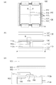
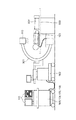
【解決手段】 各々が、複数の光電変換素子115がアレイ状に配列された第1面112aと対向する第2面112bとをつなぐ側面112cを有し、隣接して配置された複数のセンサ基板112と、複数のセンサ基板112の第1面112a側に配置されたシンチレータ120と、複数のセンサ基板112とシンチレータ120とを接着するための接着部材130と、を有し、接着部材130が、複数のセンサ基板112の間において、第1面112aから側面112cの少なくとも一部に跨って連続して接着するように、第1面112a及び側面112cの少なくとも一部に接着している。
【選択図】 図1
Description
そこで、本発明では、複数のセンサ基板の端部と接着部材との接着不良が抑制された放射線検出装置を提供することを目的とする。
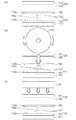
センサ基板112には、第1面112aに複数のフォトダイオードがアレイ状に配列された、厚さ500μmの単結晶シリコン基板を用いる。シンチレータ120は、厚さ300μmのAlの基台121と、厚さ800μmのCsI:Tlのシンチレータ層122と、厚さ25μmのポリパラキシリレンのシンチレータ保護層123と、を含む。センサ基板112は厚さ1.8mmのガラス基板の基台11に、厚さ1.5mmのポリオレフィン系発泡体である伸縮材161を用いた固定部材113によって固定されている。シンチレータ120と複数のセンサ基板112の第1面112aの間には、厚さ25μmのアクリル系樹脂を用いた接着部材130が配置される。そして、図2(b)に示すように、回転し得るローラー150を用いて、0.4MPaの圧力で加圧することにより、接着部材130は、センサ基板112の側面112cの第1面112a側から5μmの位置まで接着される。
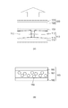
センサ基板112、シンチレータ120、及び、固定部材113は実施例1と同様のものを用いている。シンチレータ120と複数のセンサ基板112の第1面112aの間には、厚さ25μmのエチレン−メタクリル酸エステル共重合体を主成分とするホットメルト樹脂を用いた接着部材130が配置される。そして、図2(c)に示すように、100〜120℃に加熱された圧着構造体151を用いて、0.4MPaの圧力で加圧することにより、接着部材130は、センサ基板112の側面112cの第1面112a側から50μmの位置まで接着される。
シンチレータ120、接着部材130、及び、固定部材113は実施例1と同様のものを用いている。センサ基板112は、図3に示すように、第1面の端5μmにわたって角部が除去されて第3面112dを有している以外は、実施例1と同様のものを用いている。そして、実施例1と同様に、回転し得るローラー150を用いて、0.4MPaの圧力で加圧することにより、接着部材130は、センサ基板112の側面112cの第1面112a側から7μmの位置まで接着される。
シンチレータ120、接着部材130、及び、固定部材113は実施例1と同様のものを用いている。センサ基板112は、図4(b)に示すように、1度の角度Dをもってセンサ基板112の内側に向かって傾斜している以外は、実施例1と同様のものを用いている。そして、実施例1と同様に、回転し得るローラー150を用いて、0.4MPaの圧力で加圧することにより、接着部材130は、センサ基板112の側面112cの第1面112a側から4μmの位置まで接着される。
111 基台
112 センサ基板
112a 第1面
112b 第2面
112c 第3面
115 光電変換素子
120 シンチレータ
121 基材
122 シンチレータ層
150 ローラー
Claims (12)
- 各々が、複数の光電変換素子がアレイ状に配列された第1面と、当該第1面と対向する第2面と、前記第1面及び前記第2面とをつなぐ側面と、を有し、隣接して配置された複数のセンサ基板と、
前記複数のセンサ基板の前記第1面側に配置されたシンチレータと、
前記複数のセンサ基板と前記シンチレータとを接着するための接着部材と、
を有し、
前記接着部材が、前記複数のセンサ基板の間において、前記第1面から前記側面の少なくとも一部に跨って連続して接着するように、前記第1面及び前記側面の少なくとも一部に接着していることを特徴とする放射線検出装置。 - 前記複数のセンサ基板のうちの少なくとも一つが、前記複数のセンサ基板の間において、前記第1面と前記側面の間に前記第1面及び前記側面とは平行ではない第3面を有し、
前記接着部材は、前記複数のセンサ基板の間において、前記第1面から前記第3面及び前記側面の少なくとも一部に跨って連続して接着されることを特徴とする請求項1に記載の放射線検出装置。 - 前記複数のセンサ基板の間において、前記複数のセンサ基板のうちの少なくとも一つのセンサ基板の側面が、前記第1面に対して垂直な垂線に対して、前記第1面から前記第2面に向かって、前記少なくとも一つのセンサ基板の内側に向かって傾斜していることを特徴とする請求項1又は2に記載の放射線検出装置。
- 前記複数のセンサ基板を支持する基台と、
前記複数のセンサ基板を前記基台に固定するための固定部材と、
を更に有し、
前記固定部材の剛性が前記接着部材の剛性よりも低いことを特徴とする請求項1から3のいずれか1項に記載の放射線検出装置。 - 前記複数のセンサ基板は、前記第1面の前記複数の光電変換素子の周囲の少なくとも一部に配置されたガードリングと、前記ガードリングの一部及び前記複数の光電変換素子を覆うパッシベーション膜と、前記パッシベーション膜の端部を除いて前記パッシベーション膜を覆う保護層と、を更に有し、
前記接着部材は、前記複数のセンサ基板の間において、前記保護層と前記パッシベーション膜と前記ガードリングと前記第1面と前記側面の少なくとも一部に跨って連続して接着していることを特徴とする、請求項1から4のいずれか1項に記載の放射線検出装置。 - 請求項1から5のいずれか1項に記載の放射線検出装置と、
前記放射線検出装置で得られた信号に基づく画像を表示する表示装置と、
を有することを特徴とする放射線検出システム。 - 各々が、複数の光電変換素子がアレイ状に配列された第1面と、当該第1面と対向する第2面と、前記第1面及び前記第2面とをつなぐ側面と、を有し、隣接して配置された複数のセンサ基板の前記第1面側に接着部材を介してシンチレータを配置する配置工程と、
前記シンチレータの前記複数のセンサ基板の間に対応する領域を、前記複数のセンサ基板と反対側から加圧することにより、前記複数のセンサ基板の間において、前記接着部材を前記第1面から前記側面の少なくとも一部に跨って連続して接着させる接着工程と、
を行う放射線検出装置の製造方法。 - 前記複数のセンサ基板のうちの少なくとも一つが、前記複数のセンサ基板の間において、前記第1面と前記側面の間に前記第1面及び前記側面とは平行ではない第3面を有しており、
前記接着工程は、前記複数のセンサ基板の間において、前記接着部材を前記第1面から前記第3面及び前記側面の少なくとも一部に跨って連続して接着させることを特徴とする請求項7に記載の放射線検出装置の製造方法。 - 前記複数のセンサ基板の間において、前記複数のセンサ基板のうちの少なくとも一つのセンサ基板の側面が、前記第1面に対して垂直な垂線に対して、前記第1面から前記第2面に向かって、前記少なくとも一つのセンサ基板の内側に向かって傾斜していることを特徴とする請求項7又は8に記載の放射線検出装置の製造方法。
- 前記複数のセンサ基板を基台に固定部材を用いて固定させる固定工程を更に含み、
前記固定部材の剛性が前記接着部材の剛性よりも低いことを特徴とする請求項7から9のいずれか1項に記載の放射線検出装置の製造方法。 - 前記複数のセンサ基板は、前記第1面の前記複数の光電変換素子の周囲の少なくとも一部に配置されたガードリングと、前記ガードリングの一部及び前記複数の光電変換素子を覆うパッシベーション膜と、前記パッシベーション膜の端部を除いて前記パッシベーション膜を覆う保護層と、を更に有し、
前記接着工程は、前記複数のセンサ基板の間において、前記接着部材を前記保護層と前記パッシベーション膜と前記ガードリングと前記第1面と前記側面の少なくとも一部に跨って連続して接着させることを特徴とする請求項7から10のいずれか1項に記載の放射線検出装置の製造方法。 - 前記接着工程は、ローラーを用いて、前記複数のセンサ基板の間に対応する領域を前記複数のセンサ基板と反対側から加圧することを特徴とする請求項7から11のいずれか1項に記載の放射線検出装置の製造方法。
Priority Applications (10)
| Application Number | Priority Date | Filing Date | Title |
|---|---|---|---|
| JP2013258139A JP6270450B2 (ja) | 2013-12-13 | 2013-12-13 | 放射線検出装置、放射線検出システム、及び、放射線検出装置の製造方法 |
| KR1020167017969A KR101818874B1 (ko) | 2013-12-13 | 2014-10-30 | 방사선 검출 장치, 방사선 검출 시스템 및 방사선 검출 장치의 제조 방법 |
| US15/103,247 US20160291172A1 (en) | 2013-12-13 | 2014-10-30 | Radiation detecting device, radiation detecting system, and method for manufacturing the radiation detecting device |
| DE112014005663.4T DE112014005663B4 (de) | 2013-12-13 | 2014-10-30 | Strahlungserfassungsvorrichtung, Strahlungserfassungssystem und Verfahren zur Herstellung der Strahlungserfassungsvorrichtung |
| PCT/JP2014/078874 WO2015087636A1 (ja) | 2013-12-13 | 2014-10-30 | 放射線検出装置、放射線検出システム、及び、放射線検出装置の製造方法 |
| CN201811096760.1A CN109239761B (zh) | 2013-12-13 | 2014-10-30 | 辐射检测装置、辐射检测系统、以及用于制造辐射检测装置的方法 |
| CN201480068223.XA CN105829916B (zh) | 2013-12-13 | 2014-10-30 | 辐射检测装置、辐射检测系统、以及用于制造辐射检测装置的方法 |
| CN201910219458.9A CN110045410B (zh) | 2013-12-13 | 2014-10-30 | 辐射检测装置及其制造方法、辐射检测系统 |
| GB1612140.2A GB2536394B (en) | 2013-12-13 | 2014-10-30 | Radiation detecting device, and radiation detecting system |
| US16/794,731 US11226419B2 (en) | 2013-12-13 | 2020-02-19 | Radiation detecting device, radiation detecting system, and method for manufacturing the radiation detecting device |
Applications Claiming Priority (1)
| Application Number | Priority Date | Filing Date | Title |
|---|---|---|---|
| JP2013258139A JP6270450B2 (ja) | 2013-12-13 | 2013-12-13 | 放射線検出装置、放射線検出システム、及び、放射線検出装置の製造方法 |
Publications (3)
| Publication Number | Publication Date |
|---|---|
| JP2015114268A true JP2015114268A (ja) | 2015-06-22 |
| JP2015114268A5 JP2015114268A5 (ja) | 2017-01-26 |
| JP6270450B2 JP6270450B2 (ja) | 2018-01-31 |
Family
ID=53370953
Family Applications (1)
| Application Number | Title | Priority Date | Filing Date |
|---|---|---|---|
| JP2013258139A Active JP6270450B2 (ja) | 2013-12-13 | 2013-12-13 | 放射線検出装置、放射線検出システム、及び、放射線検出装置の製造方法 |
Country Status (7)
| Country | Link |
|---|---|
| US (2) | US20160291172A1 (ja) |
| JP (1) | JP6270450B2 (ja) |
| KR (1) | KR101818874B1 (ja) |
| CN (3) | CN109239761B (ja) |
| DE (1) | DE112014005663B4 (ja) |
| GB (1) | GB2536394B (ja) |
| WO (1) | WO2015087636A1 (ja) |
Cited By (2)
| Publication number | Priority date | Publication date | Assignee | Title |
|---|---|---|---|---|
| JP2019027950A (ja) * | 2017-07-31 | 2019-02-21 | キヤノン株式会社 | 放射線検出装置、放射線検出システム、及び放射線出装置の製造方法 |
| EP3599486A1 (en) | 2018-07-23 | 2020-01-29 | Canon Kabushiki Kaisha | Radiation imaging apparatus, manufacturing method thereof, and radiation imaging system |
Families Citing this family (4)
| Publication number | Priority date | Publication date | Assignee | Title |
|---|---|---|---|---|
| JP6601825B2 (ja) | 2018-04-06 | 2019-11-06 | 株式会社EmbodyMe | 画像処理装置および2次元画像生成用プログラム |
| EP4039193B1 (en) * | 2019-09-30 | 2025-08-13 | FUJIFILM Corporation | Radiation imaging device and radiation imaging device control method |
| US20240021443A1 (en) * | 2020-12-04 | 2024-01-18 | Resonac Corporation | Curable resin film, film material for semiconductor device production, curable resin composition for semiconductor device production, and method for producing semiconductor device |
| JP7608148B2 (ja) * | 2020-12-23 | 2025-01-06 | 浜松ホトニクス株式会社 | 放射線検出器、放射線検出器の製造方法、及びシンチレータパネルユニット |
Citations (10)
| Publication number | Priority date | Publication date | Assignee | Title |
|---|---|---|---|---|
| JPH07235652A (ja) * | 1993-12-29 | 1995-09-05 | E I Du Pont De Nemours & Co | X線イメージ捕獲エレメントおよびその製造方法 |
| JP2002511944A (ja) * | 1997-07-15 | 2002-04-16 | ディレクト レディオグラフィ コーポレーション | ディジタル式放射線写真パネルの製造方法 |
| JP2003017676A (ja) * | 2001-04-27 | 2003-01-17 | Canon Inc | 放射線撮像装置およびそれを用いた放射線撮像システム |
| JP2004303925A (ja) * | 2003-03-31 | 2004-10-28 | Canon Inc | 撮像用基板 |
| JP2006278877A (ja) * | 2005-03-30 | 2006-10-12 | Canon Inc | 放射線撮像装置及びその製造方法 |
| JP2008286785A (ja) * | 2007-04-18 | 2008-11-27 | Canon Inc | 放射線検出装置及び放射線検出システム |
| JP2010249722A (ja) * | 2009-04-17 | 2010-11-04 | Konica Minolta Medical & Graphic Inc | 放射線画像検出カセッテ |
| JP2012007948A (ja) * | 2010-06-23 | 2012-01-12 | Canon Inc | 放射線撮像装置、放射線撮像システム及び放射線撮像装置の製造方法 |
| JP2012189487A (ja) * | 2011-03-11 | 2012-10-04 | Fujifilm Corp | 放射線撮影装置 |
| JP2013002887A (ja) * | 2011-06-14 | 2013-01-07 | Canon Inc | 放射線検出パネルおよび放射線撮影装置 |
Family Cites Families (17)
| Publication number | Priority date | Publication date | Assignee | Title |
|---|---|---|---|---|
| EP1258739B1 (en) * | 2000-02-25 | 2008-08-06 | Hamamatsu Photonics K.K. | X-ray imaging device and method of manufacture thereof |
| US6504158B2 (en) * | 2000-12-04 | 2003-01-07 | General Electric Company | Imaging array minimizing leakage currents |
| JP2002341042A (ja) * | 2001-05-21 | 2002-11-27 | Canon Inc | 光電変換装置 |
| JP4789372B2 (ja) * | 2001-08-27 | 2011-10-12 | キヤノン株式会社 | 放射線検出装置、システム及びそれらに備えられるシンチレータパネル |
| JP2006052979A (ja) * | 2004-08-10 | 2006-02-23 | Canon Inc | 放射線検出装置及びシンチレータパネル |
| JP2007017215A (ja) * | 2005-07-06 | 2007-01-25 | Fujifilm Holdings Corp | 放射線像変換パネルの製造方法 |
| US7828926B1 (en) * | 2006-04-04 | 2010-11-09 | Radiation Monitoring Devices, Inc. | Selective removal of resin coatings and related methods |
| US8003950B2 (en) * | 2008-01-18 | 2011-08-23 | Kabushiki Kaisha Toshiba | Radiation detector, X-ray CT apparatus, and method for manufacturing radiation detector |
| JP2010008123A (ja) * | 2008-06-25 | 2010-01-14 | Panasonic Electric Works Co Ltd | センサモジュール |
| RU2510520C2 (ru) * | 2008-11-21 | 2014-03-27 | Трикселль | Способ сборки ячеистого радиационного детектора |
| JP5305996B2 (ja) * | 2009-03-12 | 2013-10-02 | 株式会社東芝 | 放射線検出器およびその製造方法 |
| JP2011128085A (ja) * | 2009-12-18 | 2011-06-30 | Canon Inc | 放射線撮像装置、放射線撮像システム及び放射線撮像装置の製造方法 |
| JP5665494B2 (ja) * | 2010-06-24 | 2015-02-04 | キヤノン株式会社 | 放射線検出装置及び放射線撮像システム |
| US20120045883A1 (en) * | 2010-08-23 | 2012-02-23 | Semiconductor Energy Laboratory Co., Ltd. | Method for manufacturing soi substrate |
| JP5792958B2 (ja) * | 2011-01-13 | 2015-10-14 | キヤノン株式会社 | 放射線撮像装置、放射線撮像システム及び放射線撮像装置の製造方法 |
| JP2012168128A (ja) * | 2011-02-16 | 2012-09-06 | Canon Inc | 放射線検出装置及び放射線撮像システム |
| US20130026380A1 (en) * | 2011-07-26 | 2013-01-31 | General Electric Company | Radiation detector with angled surfaces and method of fabrication |
-
2013
- 2013-12-13 JP JP2013258139A patent/JP6270450B2/ja active Active
-
2014
- 2014-10-30 CN CN201811096760.1A patent/CN109239761B/zh active Active
- 2014-10-30 WO PCT/JP2014/078874 patent/WO2015087636A1/ja not_active Ceased
- 2014-10-30 KR KR1020167017969A patent/KR101818874B1/ko not_active Expired - Fee Related
- 2014-10-30 CN CN201480068223.XA patent/CN105829916B/zh active Active
- 2014-10-30 DE DE112014005663.4T patent/DE112014005663B4/de active Active
- 2014-10-30 CN CN201910219458.9A patent/CN110045410B/zh active Active
- 2014-10-30 US US15/103,247 patent/US20160291172A1/en not_active Abandoned
- 2014-10-30 GB GB1612140.2A patent/GB2536394B/en active Active
-
2020
- 2020-02-19 US US16/794,731 patent/US11226419B2/en active Active
Patent Citations (11)
| Publication number | Priority date | Publication date | Assignee | Title |
|---|---|---|---|---|
| JPH07235652A (ja) * | 1993-12-29 | 1995-09-05 | E I Du Pont De Nemours & Co | X線イメージ捕獲エレメントおよびその製造方法 |
| JP2002511944A (ja) * | 1997-07-15 | 2002-04-16 | ディレクト レディオグラフィ コーポレーション | ディジタル式放射線写真パネルの製造方法 |
| JP2003017676A (ja) * | 2001-04-27 | 2003-01-17 | Canon Inc | 放射線撮像装置およびそれを用いた放射線撮像システム |
| JP2004303925A (ja) * | 2003-03-31 | 2004-10-28 | Canon Inc | 撮像用基板 |
| JP2006278877A (ja) * | 2005-03-30 | 2006-10-12 | Canon Inc | 放射線撮像装置及びその製造方法 |
| JP2008286785A (ja) * | 2007-04-18 | 2008-11-27 | Canon Inc | 放射線検出装置及び放射線検出システム |
| US20100102236A1 (en) * | 2007-04-18 | 2010-04-29 | Masato Inoue | Radiation detecting apparatus and radiation detecting system |
| JP2010249722A (ja) * | 2009-04-17 | 2010-11-04 | Konica Minolta Medical & Graphic Inc | 放射線画像検出カセッテ |
| JP2012007948A (ja) * | 2010-06-23 | 2012-01-12 | Canon Inc | 放射線撮像装置、放射線撮像システム及び放射線撮像装置の製造方法 |
| JP2012189487A (ja) * | 2011-03-11 | 2012-10-04 | Fujifilm Corp | 放射線撮影装置 |
| JP2013002887A (ja) * | 2011-06-14 | 2013-01-07 | Canon Inc | 放射線検出パネルおよび放射線撮影装置 |
Cited By (4)
| Publication number | Priority date | Publication date | Assignee | Title |
|---|---|---|---|---|
| JP2019027950A (ja) * | 2017-07-31 | 2019-02-21 | キヤノン株式会社 | 放射線検出装置、放射線検出システム、及び放射線出装置の製造方法 |
| EP3599486A1 (en) | 2018-07-23 | 2020-01-29 | Canon Kabushiki Kaisha | Radiation imaging apparatus, manufacturing method thereof, and radiation imaging system |
| JP2020016478A (ja) * | 2018-07-23 | 2020-01-30 | キヤノン株式会社 | 放射線撮像装置、その製造方法及び放射線撮像システム |
| US11086030B2 (en) | 2018-07-23 | 2021-08-10 | Canon Kabushiki Kaisha | Radiation imaging apparatus, manufacturing method thereof, and radiation imaging system |
Also Published As
| Publication number | Publication date |
|---|---|
| GB2536394A (en) | 2016-09-14 |
| CN105829916B (zh) | 2019-04-02 |
| JP6270450B2 (ja) | 2018-01-31 |
| KR20160094438A (ko) | 2016-08-09 |
| CN110045410A (zh) | 2019-07-23 |
| DE112014005663B4 (de) | 2025-08-21 |
| GB201612140D0 (en) | 2016-08-24 |
| CN109239761A (zh) | 2019-01-18 |
| KR101818874B1 (ko) | 2018-01-15 |
| US20200183022A1 (en) | 2020-06-11 |
| US11226419B2 (en) | 2022-01-18 |
| US20160291172A1 (en) | 2016-10-06 |
| CN110045410B (zh) | 2023-01-03 |
| WO2015087636A1 (ja) | 2015-06-18 |
| CN109239761B (zh) | 2023-01-10 |
| DE112014005663T5 (de) | 2016-09-15 |
| CN105829916A (zh) | 2016-08-03 |
| GB2536394B (en) | 2020-12-09 |
Similar Documents
| Publication | Publication Date | Title |
|---|---|---|
| US11226419B2 (en) | Radiation detecting device, radiation detecting system, and method for manufacturing the radiation detecting device | |
| US8957383B2 (en) | Radiation detection apparatus and radiation detection system | |
| US9568614B2 (en) | Radiation detection apparatus, method of manufacturing the same, and imaging system | |
| US9081104B2 (en) | Radiation detection apparatus and radiation detection system | |
| JP5607426B2 (ja) | 放射線検出装置及び放射線撮像システム | |
| JP5693173B2 (ja) | 放射線検出装置及び放射線検出システム | |
| JP4464260B2 (ja) | 半導体装置、放射線撮像装置、及びその製造方法 | |
| EP3566248B1 (en) | Detach and reattach of a flexible polyimide based x-ray detector | |
| US10345455B2 (en) | Radiation detection apparatus, radiation imaging system, and method of manufacturing radiation detection apparatus | |
| US20120318990A1 (en) | Radiation detection panel and radiation imaging apparatus | |
| JP2006220439A (ja) | シンチレータパネル、放射線検出装置及びその製造方法 | |
| JP2007071836A (ja) | 放射線検出装置及び放射線撮像システム | |
| JP4819344B2 (ja) | 半導体装置、放射線撮像装置、及びその製造方法 | |
| JP2021056092A (ja) | 放射線撮像装置 | |
| JP2007057428A (ja) | 放射線検出装置及び放射線撮像システム | |
| JP5403848B2 (ja) | 放射線検出装置及び放射線検出システム | |
| JP2022092706A (ja) | 放射線検出装置の製造方法 | |
| JP2022092707A (ja) | 放射線検出装置の製造方法 | |
| JP2021071378A (ja) | 放射線検出装置の製造方法 | |
| KR20200019478A (ko) | X선 디텍터 | |
| JP2017190981A (ja) | 放射線撮像装置及びその製造方法、並びに、放射線撮像システム | |
| JP2016109494A (ja) | 放射線検出装置及び放射線検出システム |
Legal Events
| Date | Code | Title | Description |
|---|---|---|---|
| A521 | Request for written amendment filed |
Free format text: JAPANESE INTERMEDIATE CODE: A523 Effective date: 20161209 |
|
| A621 | Written request for application examination |
Free format text: JAPANESE INTERMEDIATE CODE: A621 Effective date: 20161209 |
|
| A131 | Notification of reasons for refusal |
Free format text: JAPANESE INTERMEDIATE CODE: A131 Effective date: 20170829 |
|
| A521 | Request for written amendment filed |
Free format text: JAPANESE INTERMEDIATE CODE: A523 Effective date: 20170915 |
|
| TRDD | Decision of grant or rejection written | ||
| A01 | Written decision to grant a patent or to grant a registration (utility model) |
Free format text: JAPANESE INTERMEDIATE CODE: A01 Effective date: 20171128 |
|
| A61 | First payment of annual fees (during grant procedure) |
Free format text: JAPANESE INTERMEDIATE CODE: A61 Effective date: 20171226 |
|
| R151 | Written notification of patent or utility model registration |
Ref document number: 6270450 Country of ref document: JP Free format text: JAPANESE INTERMEDIATE CODE: R151 |