JP2011248351A - Liquid crystal display device - Google Patents
Liquid crystal display device Download PDFInfo
- Publication number
- JP2011248351A JP2011248351A JP2011099642A JP2011099642A JP2011248351A JP 2011248351 A JP2011248351 A JP 2011248351A JP 2011099642 A JP2011099642 A JP 2011099642A JP 2011099642 A JP2011099642 A JP 2011099642A JP 2011248351 A JP2011248351 A JP 2011248351A
- Authority
- JP
- Japan
- Prior art keywords
- light
- liquid crystal
- transistor
- crystal display
- display device
- Prior art date
- Legal status (The legal status is an assumption and is not a legal conclusion. Google has not performed a legal analysis and makes no representation as to the accuracy of the status listed.)
- Withdrawn
Links
Images


Classifications
-
- G—PHYSICS
- G02—OPTICS
- G02F—OPTICAL DEVICES OR ARRANGEMENTS FOR THE CONTROL OF LIGHT BY MODIFICATION OF THE OPTICAL PROPERTIES OF THE MEDIA OF THE ELEMENTS INVOLVED THEREIN; NON-LINEAR OPTICS; FREQUENCY-CHANGING OF LIGHT; OPTICAL LOGIC ELEMENTS; OPTICAL ANALOGUE/DIGITAL CONVERTERS
- G02F1/00—Devices or arrangements for the control of the intensity, colour, phase, polarisation or direction of light arriving from an independent light source, e.g. switching, gating or modulating; Non-linear optics
- G02F1/01—Devices or arrangements for the control of the intensity, colour, phase, polarisation or direction of light arriving from an independent light source, e.g. switching, gating or modulating; Non-linear optics for the control of the intensity, phase, polarisation or colour
- G02F1/13—Devices or arrangements for the control of the intensity, colour, phase, polarisation or direction of light arriving from an independent light source, e.g. switching, gating or modulating; Non-linear optics for the control of the intensity, phase, polarisation or colour based on liquid crystals, e.g. single liquid crystal display cells
- G02F1/133—Constructional arrangements; Operation of liquid crystal cells; Circuit arrangements
-
- G—PHYSICS
- G09—EDUCATION; CRYPTOGRAPHY; DISPLAY; ADVERTISING; SEALS
- G09G—ARRANGEMENTS OR CIRCUITS FOR CONTROL OF INDICATING DEVICES USING STATIC MEANS TO PRESENT VARIABLE INFORMATION
- G09G3/00—Control arrangements or circuits, of interest only in connection with visual indicators other than cathode-ray tubes
- G09G3/20—Control arrangements or circuits, of interest only in connection with visual indicators other than cathode-ray tubes for presentation of an assembly of a number of characters, e.g. a page, by composing the assembly by combination of individual elements arranged in a matrix no fixed position being assigned to or needed to be assigned to the individual characters or partial characters
- G09G3/34—Control arrangements or circuits, of interest only in connection with visual indicators other than cathode-ray tubes for presentation of an assembly of a number of characters, e.g. a page, by composing the assembly by combination of individual elements arranged in a matrix no fixed position being assigned to or needed to be assigned to the individual characters or partial characters by control of light from an independent source
- G09G3/3406—Control of illumination source
-
- G—PHYSICS
- G02—OPTICS
- G02F—OPTICAL DEVICES OR ARRANGEMENTS FOR THE CONTROL OF LIGHT BY MODIFICATION OF THE OPTICAL PROPERTIES OF THE MEDIA OF THE ELEMENTS INVOLVED THEREIN; NON-LINEAR OPTICS; FREQUENCY-CHANGING OF LIGHT; OPTICAL LOGIC ELEMENTS; OPTICAL ANALOGUE/DIGITAL CONVERTERS
- G02F1/00—Devices or arrangements for the control of the intensity, colour, phase, polarisation or direction of light arriving from an independent light source, e.g. switching, gating or modulating; Non-linear optics
- G02F1/01—Devices or arrangements for the control of the intensity, colour, phase, polarisation or direction of light arriving from an independent light source, e.g. switching, gating or modulating; Non-linear optics for the control of the intensity, phase, polarisation or colour
- G02F1/13—Devices or arrangements for the control of the intensity, colour, phase, polarisation or direction of light arriving from an independent light source, e.g. switching, gating or modulating; Non-linear optics for the control of the intensity, phase, polarisation or colour based on liquid crystals, e.g. single liquid crystal display cells
- G02F1/133—Constructional arrangements; Operation of liquid crystal cells; Circuit arrangements
- G02F1/1333—Constructional arrangements; Manufacturing methods
- G02F1/1335—Structural association of cells with optical devices, e.g. polarisers or reflectors
-
- G—PHYSICS
- G09—EDUCATION; CRYPTOGRAPHY; DISPLAY; ADVERTISING; SEALS
- G09G—ARRANGEMENTS OR CIRCUITS FOR CONTROL OF INDICATING DEVICES USING STATIC MEANS TO PRESENT VARIABLE INFORMATION
- G09G3/00—Control arrangements or circuits, of interest only in connection with visual indicators other than cathode-ray tubes
- G09G3/20—Control arrangements or circuits, of interest only in connection with visual indicators other than cathode-ray tubes for presentation of an assembly of a number of characters, e.g. a page, by composing the assembly by combination of individual elements arranged in a matrix no fixed position being assigned to or needed to be assigned to the individual characters or partial characters
- G09G3/34—Control arrangements or circuits, of interest only in connection with visual indicators other than cathode-ray tubes for presentation of an assembly of a number of characters, e.g. a page, by composing the assembly by combination of individual elements arranged in a matrix no fixed position being assigned to or needed to be assigned to the individual characters or partial characters by control of light from an independent source
- G09G3/36—Control arrangements or circuits, of interest only in connection with visual indicators other than cathode-ray tubes for presentation of an assembly of a number of characters, e.g. a page, by composing the assembly by combination of individual elements arranged in a matrix no fixed position being assigned to or needed to be assigned to the individual characters or partial characters by control of light from an independent source using liquid crystals
- G09G3/3611—Control of matrices with row and column drivers
- G09G3/3648—Control of matrices with row and column drivers using an active matrix
-
- G—PHYSICS
- G09—EDUCATION; CRYPTOGRAPHY; DISPLAY; ADVERTISING; SEALS
- G09G—ARRANGEMENTS OR CIRCUITS FOR CONTROL OF INDICATING DEVICES USING STATIC MEANS TO PRESENT VARIABLE INFORMATION
- G09G2300/00—Aspects of the constitution of display devices
- G09G2300/08—Active matrix structure, i.e. with use of active elements, inclusive of non-linear two terminal elements, in the pixels together with light emitting or modulating elements
- G09G2300/0809—Several active elements per pixel in active matrix panels
- G09G2300/0842—Several active elements per pixel in active matrix panels forming a memory circuit, e.g. a dynamic memory with one capacitor
-
- G—PHYSICS
- G09—EDUCATION; CRYPTOGRAPHY; DISPLAY; ADVERTISING; SEALS
- G09G—ARRANGEMENTS OR CIRCUITS FOR CONTROL OF INDICATING DEVICES USING STATIC MEANS TO PRESENT VARIABLE INFORMATION
- G09G2320/00—Control of display operating conditions
- G09G2320/02—Improving the quality of display appearance
- G09G2320/0209—Crosstalk reduction, i.e. to reduce direct or indirect influences of signals directed to a certain pixel of the displayed image on other pixels of said image, inclusive of influences affecting pixels in different frames or fields or sub-images which constitute a same image, e.g. left and right images of a stereoscopic display
- G09G2320/0214—Crosstalk reduction, i.e. to reduce direct or indirect influences of signals directed to a certain pixel of the displayed image on other pixels of said image, inclusive of influences affecting pixels in different frames or fields or sub-images which constitute a same image, e.g. left and right images of a stereoscopic display with crosstalk due to leakage current of pixel switch in active matrix panels
-
- G—PHYSICS
- G09—EDUCATION; CRYPTOGRAPHY; DISPLAY; ADVERTISING; SEALS
- G09G—ARRANGEMENTS OR CIRCUITS FOR CONTROL OF INDICATING DEVICES USING STATIC MEANS TO PRESENT VARIABLE INFORMATION
- G09G2320/00—Control of display operating conditions
- G09G2320/02—Improving the quality of display appearance
- G09G2320/0233—Improving the luminance or brightness uniformity across the screen
-
- G—PHYSICS
- G09—EDUCATION; CRYPTOGRAPHY; DISPLAY; ADVERTISING; SEALS
- G09G—ARRANGEMENTS OR CIRCUITS FOR CONTROL OF INDICATING DEVICES USING STATIC MEANS TO PRESENT VARIABLE INFORMATION
- G09G2320/00—Control of display operating conditions
- G09G2320/04—Maintaining the quality of display appearance
- G09G2320/041—Temperature compensation
-
- G—PHYSICS
- G09—EDUCATION; CRYPTOGRAPHY; DISPLAY; ADVERTISING; SEALS
- G09G—ARRANGEMENTS OR CIRCUITS FOR CONTROL OF INDICATING DEVICES USING STATIC MEANS TO PRESENT VARIABLE INFORMATION
- G09G2320/00—Control of display operating conditions
- G09G2320/10—Special adaptations of display systems for operation with variable images
-
- G—PHYSICS
- G09—EDUCATION; CRYPTOGRAPHY; DISPLAY; ADVERTISING; SEALS
- G09G—ARRANGEMENTS OR CIRCUITS FOR CONTROL OF INDICATING DEVICES USING STATIC MEANS TO PRESENT VARIABLE INFORMATION
- G09G2330/00—Aspects of power supply; Aspects of display protection and defect management
- G09G2330/02—Details of power systems and of start or stop of display operation
- G09G2330/021—Power management, e.g. power saving
- G09G2330/023—Power management, e.g. power saving using energy recovery or conservation
-
- G—PHYSICS
- G09—EDUCATION; CRYPTOGRAPHY; DISPLAY; ADVERTISING; SEALS
- G09G—ARRANGEMENTS OR CIRCUITS FOR CONTROL OF INDICATING DEVICES USING STATIC MEANS TO PRESENT VARIABLE INFORMATION
- G09G2340/00—Aspects of display data processing
- G09G2340/04—Changes in size, position or resolution of an image
- G09G2340/0407—Resolution change, inclusive of the use of different resolutions for different screen areas
- G09G2340/0435—Change or adaptation of the frame rate of the video stream
Abstract
Description
本発明は、液晶表示装置に関する。特に、透過型の液晶表示装置に関する。 The present invention relates to a liquid crystal display device. In particular, the present invention relates to a transmissive liquid crystal display device.
液晶表示装置は、印加される電圧に応じて配向が制御される液晶材料を光の変調に利用することで表示を行う装置である。さらに、液晶表示装置は、表示に利用する光によって2種類に大別される。具体的には、液晶表示装置は、自然光又は屋内用照明などの外光、及び液晶表示装置自体に設けられる光源(バックライト)から発光される光のいずれを利用するかによって2種類に大別される。一般的に、前者を利用して表示を行う液晶表示装置は、反射型の液晶表示装置と呼ばれ、後者を利用して表示を行う液晶表示装置は、透過型の液晶表示装置と呼ばれる。なお、反射型の液晶表示装置は、外部環境(外光)に依存して表示の特質が変化するため、透過型の液晶表示装置の方が装置としての汎用性が高い。 A liquid crystal display device is a device that performs display by using a liquid crystal material whose orientation is controlled in accordance with an applied voltage for light modulation. Furthermore, liquid crystal display devices are roughly classified into two types depending on the light used for display. Specifically, liquid crystal display devices are roughly classified into two types depending on whether natural light or outside light such as indoor lighting, or light emitted from a light source (backlight) provided in the liquid crystal display device itself is used. Is done. In general, a liquid crystal display device that performs display using the former is referred to as a reflective liquid crystal display device, and a liquid crystal display device that performs display using the latter is referred to as a transmissive liquid crystal display device. Note that a reflective liquid crystal display device changes in display characteristics depending on an external environment (external light), and thus a transmissive liquid crystal display device has higher versatility as a device.
一般的な透過型の液晶表示装置は、マトリクス状に配設された複数の画素が設けられた表示パネルと、該表示パネルに対して白色光を発するバックライトとを有する。さらに、当該画素には、画像信号の入力を制御するトランジスタと、画像信号に応じた電圧が印加される液晶素子と、特定色を呈する波長の光のみを透過するカラーフィルター(例えば、赤色(R)、緑色(G)、青色(B))とが設けられる。なお、液晶素子は、一対の電極と、該一対の電極に挟持された液晶材料とを有する。そして、画素毎に白色光の透過率を制御し、且つカラーフィルターによって特定色を呈する波長の光のみを透過させることで各画素における表示が決定される。これにより、当該液晶表示装置が有する表示パネルにおいて画像が表示される。 A typical transmissive liquid crystal display device includes a display panel provided with a plurality of pixels arranged in a matrix, and a backlight that emits white light to the display panel. The pixel further includes a transistor that controls input of an image signal, a liquid crystal element to which a voltage corresponding to the image signal is applied, and a color filter that transmits only light having a wavelength exhibiting a specific color (for example, red (R ), Green (G), and blue (B)). Note that the liquid crystal element includes a pair of electrodes and a liquid crystal material sandwiched between the pair of electrodes. And the display in each pixel is determined by controlling the transmittance | permeability of white light for every pixel and transmitting only the light of the wavelength which exhibits a specific color with a color filter. Thereby, an image is displayed on the display panel of the liquid crystal display device.
近年では、地球環境への関心が高まり、低消費電力型の液晶表示装置の開発が注目されている。例えば、特許文献1では、液晶表示装置における消費電力を低減する技術が開示されている。具体的には、全ての走査線及びデータ信号線を非選択状態とする休止期間に、全データ信号線を電気的にデータ信号ドライバから切り離して不定状態(浮遊状態、フローティング状態ともいう)とする液晶表示装置が開示されている。
In recent years, interest in the global environment has increased, and attention has been paid to the development of low power consumption liquid crystal display devices. For example,
特許文献1で開示される液晶表示装置では、休止期間において、画素に対する画像信号の入力が行われない。すなわち、各画素内に画像信号を保持したまま、画像信号の入力を制御するトランジスタがオフ状態を維持する期間が長期化する。そのため、当該トランジスタのオフ電流が画素の表示に対して与える影響が顕在化する。具体的には、液晶素子に印加される電圧が低下し、当該液晶素子を有する画素の表示の劣化(変化)が顕在化する。
In the liquid crystal display device disclosed in
ところで、透過型の液晶表示装置は、表示パネルと、該表示パネルに近接するバックライトとを有する。該バックライトは、発光時に発熱を伴う。そのため、表示パネルに設けられたトランジスタの動作温度は、当該バックライトの発光に伴い上昇することになる。なお、トランジスタのオフ電流は、動作温度の上昇に伴い増加する。すなわち、特許文献1で開示される液晶表示装置として透過型の液晶表示装置を適用する場合、消費電力と表示品質の間に強いトレードオフの関係が存在することになる。
Incidentally, a transmissive liquid crystal display device includes a display panel and a backlight adjacent to the display panel. The backlight generates heat during light emission. Therefore, the operating temperature of the transistor provided in the display panel increases with the light emission of the backlight. Note that the off-state current of the transistor increases with an increase in operating temperature. That is, when a transmissive liquid crystal display device is applied as the liquid crystal display device disclosed in
そこで、本発明の一態様は、透過型の液晶表示装置において、消費電力の低減及び表示品質の低下の抑制を両立させることを課題の一とする。 In view of the above, an object of one embodiment of the present invention is to achieve both reduction of power consumption and suppression of deterioration of display quality in a transmissive liquid crystal display device.
本発明の一態様は、画素に対する画像信号の入力頻度を制御することが可能な透過型の液晶表示装置において、バックライトとして面(平面)発光を行う光源を適用することを要旨とする。 One aspect of the present invention is to apply a light source that emits surface (planar) light as a backlight in a transmissive liquid crystal display device capable of controlling an input frequency of an image signal to a pixel.
具体的には、本発明の一態様は、画像信号の入力を制御するトランジスタ、前記画像信号に応じた電圧が印加される液晶素子、及び、赤色を呈する波長領域の光を透過し且つその他の可視光領域の光を吸収するカラーフィルター、緑色を呈する波長領域の光を透過し且つその他の可視光領域の光を吸収するカラーフィルター、又は青色を呈する波長領域の光を透過し且つその他の可視光領域の光を吸収するカラーフィルターを備えた画素がマトリクス状に配設された画素部を有する表示パネルと、前記画素部に対して白色光を発するバックライトと、前記画素に対する画像信号の入力頻度を制御する制御回路と、を有し、前記バックライトは、面発光を行うことを特徴とする液晶表示装置である。 Specifically, according to one embodiment of the present invention, a transistor for controlling input of an image signal, a liquid crystal element to which a voltage corresponding to the image signal is applied, light in a wavelength region exhibiting red color, and the other A color filter that absorbs light in the visible light region, a color filter that transmits light in the green wavelength region and absorbs light in other visible light regions, or a light that transmits light in the blue wavelength region and other visible A display panel having a pixel portion in which pixels having color filters that absorb light in the light region are arranged in a matrix, a backlight that emits white light to the pixel portion, and an image signal input to the pixel And a control circuit for controlling the frequency, wherein the backlight performs surface light emission.
なお、当該面発光を行う光源は、発光を面状に行う光源である。例えば、当該光源としては、有機エレクトロルミネッセンス(有機EL)を利用して発光を行う光源などが挙げられる。また、当該光源は、点光源又は線光源からの発光を光学系によって面状に加工する光源ではない。すなわち、当該光源は、LED又は冷陰極管などからの発光を導光板、散乱板、プリズム板などによって面状に加工する光源ではない。 In addition, the light source which performs the said surface light emission is a light source which performs light emission in planar shape. For example, examples of the light source include a light source that emits light using organic electroluminescence (organic EL). The light source is not a light source that processes light emitted from a point light source or a line light source into a planar shape by an optical system. That is, the light source is not a light source that processes light emitted from an LED or a cold cathode tube into a planar shape using a light guide plate, a scattering plate, a prism plate, or the like.
本発明の一態様の液晶表示装置は、バックライトとして面発光を行う光源を適用する。当該光源は、発光を面状に行う光源であるため発光面積が広い。そのため、当該バックライトでは、放熱を効率よく行うことができる。すなわち、当該バックライトは、発光時における温度上昇が抑制されたバックライトである。これに付随して、当該液晶表示装置においては、各画素に設けられるトランジスタの動作温度の上昇を抑制することが可能である。そのため、当該液晶表示装置においては、当該トランジスタのオフ電流の値の増加を抑制することが可能である。 In the liquid crystal display device of one embodiment of the present invention, a light source that performs surface light emission is used as a backlight. Since the light source is a light source that emits light in a planar shape, the light emission area is wide. Therefore, the backlight can efficiently dissipate heat. That is, the backlight is a backlight in which a temperature rise during light emission is suppressed. Accompanying this, in the liquid crystal display device, it is possible to suppress an increase in the operating temperature of the transistor provided in each pixel. Therefore, in the liquid crystal display device, an increase in the off-state current value of the transistor can be suppressed.
上述したように本発明の一態様の液晶表示装置は、バックライトとして放熱性に優れる光源を適用する。これにより、画素に対して長期間に渡って画像信号の入力が行われない場合であっても、当該画素において画像信号を保持することが可能になる。すなわち、消費電力の低減と表示品質の低下の抑制を両立することが可能になる。 As described above, the liquid crystal display device of one embodiment of the present invention employs a light source with excellent heat dissipation as a backlight. Accordingly, even when an image signal is not input to the pixel for a long period of time, the image signal can be held in the pixel. That is, it becomes possible to achieve both reduction of power consumption and suppression of deterioration of display quality.
以下では、本発明の実施の形態について図面を用いて詳細に説明する。ただし、本発明は以下の説明に限定されず、本発明の趣旨およびその範囲から逸脱することなくその形態および詳細を様々に変更し得ることは、当業者であれば容易に理解される。したがって、本発明は以下に示す実施の形態の記載内容に限定して解釈されるものではない。 Hereinafter, embodiments of the present invention will be described in detail with reference to the drawings. However, the present invention is not limited to the following description, and it is easily understood by those skilled in the art that modes and details can be variously changed without departing from the spirit and scope of the present invention. Therefore, the present invention should not be construed as being limited to the description of the embodiments below.
まず、透過型の液晶表示装置の一例について図1〜図11を参照して説明する。 First, an example of a transmissive liquid crystal display device will be described with reference to FIGS.
<液晶表示装置の構成例>
図1(A)は、透過型の液晶表示装置の構成例を示す斜視図である。図1(A)に示す液晶表示装置は、偏光板10A及び偏光板10Bに挟持された表示パネル11と、表示パネル11に近接して設けられるバックライト12と、表示パネル11及びバックライト12を制御する制御回路13とを有する。なお、制御回路13は、FPC(Flexible Printed Circuits)14A、14Bを介して、表示パネル11及びバックライト12に電気的に接続されている。また、表示パネル11は、マトリクス状に複数の画素が配設された画素部110と、画素部110における表示を制御する走査線駆動回路111及び信号線駆動回路112とを有する。さらに、各画素は、特定色を呈する波長の光のみを透過するカラーフィルターを有する。ここでは、横方向に近接して配設された3つの画素の各々が、赤色(R)を呈する波長領域(600nm以上700nm未満)の光を透過し且つその他の可視光領域の光を吸収するカラーフィルター1102R、緑色(G)を呈する波長領域(500nm以上570nm未満)の光を透過し且つその他の可視光領域の光を吸収するカラーフィルター1102G、及び青色(B)を呈する波長領域(430nm以上500nm未満)の光を透過し且つその他の可視光領域の光を吸収するカラーフィルター1102Bのいずれか、且つ他の2つの画素が有するカラーフィルターと異なるカラーフィルターを有することとする。
<Configuration example of liquid crystal display device>
FIG. 1A is a perspective view illustrating a configuration example of a transmissive liquid crystal display device. A liquid crystal display device illustrated in FIG. 1A includes a
<表示パネル11の構成例>
図1(B)は、表示パネル11の具体的な構成例を示す図である。図1(B)に示す表示パネル11は、画素部110と、走査線駆動回路111と、信号線駆動回路112と、各々が平行又は略平行に配設され、且つ走査線駆動回路111によって電位が制御されるn本(nは、2以上の自然数)の走査線1111と、各々が平行又は略平行に配設され、且つ信号線駆動回路112によって電位が制御される、m本(mは、2以上の自然数)の信号線1121とを有する。さらに、画素部110は、マトリクス状(n行m列)に配設された複数の画素1101を有する。なお、各走査線1111は、マトリクス状(n行m列)に配設された複数の画素1101のうち、いずれかの行に配設されたm個の画素1101に電気的に接続される。また、各信号線1121は、マトリクス状(n行m列)に配設された複数の画素1101のうち、いずれかの列に配設されたn個の画素1101に電気的に接続される。
<Configuration Example of
FIG. 1B is a diagram illustrating a specific configuration example of the
なお、走査線駆動回路111には、制御回路13から走査線駆動回路用スタート信号、走査線駆動回路用クロック信号、及び高電源電位、低電源電位などの駆動用電源が入力される。また、信号線駆動回路112には、制御回路13から信号線駆動回路用スタート信号、信号線駆動回路用クロック信号、画像信号などの信号、及び高電源電位、低電源電位などの駆動用電源が入力される。
Note that the scanning
<画素1101の構成例>
図1(C)は、画素1101の回路構成例を示す図である。図1(C)に示す画素1101は、ゲートが走査線1111に電気的に接続され、ソース及びドレインの一方が信号線1121に電気的に接続されたトランジスタ11011と、一方の電極がトランジスタ11011のソース及びドレインの他方に電気的に接続され、他方の電極が容量電位を供給する配線に電気的に接続された容量素子11012と、一方の電極がトランジスタ11011のソース及びドレインの他方並びに容量素子11012の一方の電極に電気的に接続され、他方の電極が対向電位を供給する配線に電気的に接続された液晶素子11013と、を有する。
<Configuration Example of
FIG. 1C illustrates a circuit configuration example of the
<トランジスタ11011の構成例>
図2は、トランジスタ11011の構成例を示す図である。図2に示すトランジスタ11011は、絶縁表面を有する基板220上に設けられたゲート層221と、ゲート層221上に設けられたゲート絶縁層222と、ゲート絶縁層222上に設けられた酸化物半導体層223と、酸化物半導体層223上に設けられたソース層224a及びドレイン層224bとを有する。また、図2に示すトランジスタ11011においては、トランジスタ11011を覆い、酸化物半導体層223に接する絶縁層225と、絶縁層225上に設けられた保護絶縁層226とが形成されている。
<Structure Example of
FIG. 2 is a diagram illustrating a configuration example of the
図2に示すトランジスタ11011は、上記の通り、半導体層として酸化物半導体層223を具備する。酸化物半導体層223に用いる酸化物半導体としては、四元系金属酸化物であるIn−Sn−Ga−Zn−O系、三元系金属酸化物であるIn−Ga−Zn−O系、In−Sn−Zn−O系、In−Al−Zn−O系、Sn−Ga−Zn−O系、Al−Ga−Zn−O系、Sn−Al−Zn−O系、二元系金属酸化物であるIn−Ga−O系、In−Zn−O系、Sn−Zn−O系、Al−Zn−O系、Zn−Mg−O系、Sn−Mg−O系、In−Mg−O系、または単元系金属酸化物であるIn−O系、Sn−O系、Zn−O系などを用いることができる。また、上記酸化物半導体にSiO2を含んでもよい。ここで、例えば、In−Ga−Zn−O系酸化物半導体とは、少なくともInとGaとZnを含む酸化物であり、その組成比に特に制限はない。また、InとGaとZn以外の元素を含んでもよい。また、酸化物半導体層223は、化学式InMO3(ZnO)m(m>0)で表記される薄膜を用いることができる。ここで、Mは、Ga、Al、MnおよびCoから選ばれた一または複数の金属元素を示す。例えばMとして、Ga、Ga及びAl、Ga及びMn、またはGa及びCoなどを選択することができる。
The
また、酸化物半導体としてIn−Zn−O系の材料を用いる場合、用いるターゲットの組成比は、原子数比で、In:Zn=50:1〜1:2(モル数比に換算するとIn2O3:ZnO=25:1〜1:4)、好ましくはIn:Zn=20:1〜1:1(モル数比に換算するとIn2O3:ZnO=2:1〜10:1)、さらに好ましくはIn:Zn=1.5:1〜15:1(モル数比に換算するとIn2O3:ZnO=3:4〜15:2)とする。例えば、In−Zn−O系酸化物半導体の形成に用いるターゲットは、原子数比がIn:Zn:O=X:Y:Zのとき、Z>1.5X+Yとする。 In the case where an In—Zn—O-based material is used as the oxide semiconductor, the composition ratio of the target used is an atomic ratio, and In: Zn = 50: 1 to 1: 2 (in terms of the molar ratio, In 2 O 3 : ZnO = 25: 1 to 1: 4), preferably In: Zn = 20: 1 to 1: 1 (In 2 O 3 : ZnO = 2: 1 to 10: 1 in terms of molar ratio), More preferably, In: Zn = 1.5: 1 to 15: 1 (In 2 O 3 : ZnO = 3: 4 to 15: 2 in terms of molar ratio). For example, a target used for forming an In—Zn—O-based oxide semiconductor satisfies Z> 1.5X + Y when the atomic ratio is In: Zn: O = X: Y: Z.
上述した酸化物半導体は、変動要因となる水素、水分、水酸基又は水素化物(水素化合物ともいう)などの不純物を意図的に排除することで高純度化し、電気的にI型(真性)化された酸化物半導体である。これにより、当該酸化物半導体を用いたトランジスタの電気的特性変動を抑止することが可能となる。 The above-described oxide semiconductor is highly purified by intentionally removing impurities such as hydrogen, moisture, hydroxyl groups, or hydrides (also referred to as hydrogen compounds), which cause fluctuations, and is electrically i-type (intrinsic). Oxide semiconductor. Accordingly, variation in electrical characteristics of a transistor including the oxide semiconductor can be suppressed.
よって酸化物半導体中の水素は少なければ少ないほどよい。また、高純度化された酸化物半導体層中には水素や酸素欠損等に由来するキャリアが極めて少なく(ゼロに近い)、キャリア密度は1×10¹²/cm3未満、好ましくは1×1011/cm3未満である。即ち、酸化物半導体層の水素や酸素欠損等に由来するキャリア密度を限りなくゼロに近くする。酸化物半導体層中に水素や酸素欠損等に由来するキャリアが極めて少ないため、トランジスタがオフ状態のときのオフ電流を少なくすることができる。また、水素や酸素欠損等に由来する不純物準位が少ないことにより、光照射、温度変化、バイアス印加等による電気特性の変動及び劣化を少なくすることができる。なお、オフ電流は少なければ少ないほど好ましい。上記酸化物半導体を半導体層として用いたトランジスタは、チャネル幅(w)1μmあたりのオフ電流値が100zA(ゼプトアンペア)以下、好ましくは10zA以下、更に好ましくは1zA以下である。さらに、pn接合がなく、ホットキャリア劣化がないため、トランジスタの電気的特性がこれら要因の影響を受けない。 Thus, the less hydrogen in the oxide semiconductor, the better. In the highly purified oxide semiconductor layer, carriers derived from hydrogen, oxygen vacancies, and the like are very few (close to zero), and the carrier density is less than 1 × 10 12 / cm 3 , preferably 1 × 10 11. / Cm 3 or less. That is, the carrier density derived from hydrogen or oxygen vacancies in the oxide semiconductor layer is made as close to zero as possible. Since there are very few carriers derived from hydrogen, oxygen vacancies, or the like in the oxide semiconductor layer, off-state current when the transistor is off can be reduced. In addition, since there are few impurity levels derived from hydrogen, oxygen vacancies, and the like, fluctuations and deterioration of electrical characteristics due to light irradiation, temperature change, bias application, and the like can be reduced. Note that the smaller the off-state current, the better. A transistor using the oxide semiconductor as a semiconductor layer has an off-current value per channel width (w) of 1 μm of 100 zA (zeptoampere) or less, preferably 10 zA or less, and more preferably 1 zA or less. Further, since there is no pn junction and there is no hot carrier deterioration, the electrical characteristics of the transistor are not affected by these factors.
このように酸化物半導体層に含まれる水素を徹底的に除去することにより高純度化された酸化物半導体をチャネル形成領域に用いたトランジスタは、オフ電流を極めて小さくすることができる。つまり、トランジスタのオフ状態において、酸化物半導体層は絶縁体とみなして回路設計を行うことができる。一方で、酸化物半導体層は、トランジスタのオン状態においては、非晶質シリコンで形成される半導体層よりも高い電流供給能力を見込むことができる。 In this manner, a transistor in which a highly purified oxide semiconductor is used for a channel formation region by thoroughly removing hydrogen contained in the oxide semiconductor layer can have extremely low off-state current. That is, in the off state of the transistor, circuit design can be performed by regarding the oxide semiconductor layer as an insulator. On the other hand, the oxide semiconductor layer can expect higher current supply capability than the semiconductor layer formed of amorphous silicon in the on state of the transistor.
なお、基板220としては、例えば、バリウムホウケイ酸ガラスやアルミノホウケイ酸ガラスなどのガラス基板を用いることができる。
As the
また、ゲート層221としては、アルミニウム(Al)、銅(Cu)、チタン(Ti)、タンタル(Ta)、タングステン(W)、モリブデン(Mo)、クロム(Cr)、ネオジム(Nd)、スカンジウム(Sc)から選ばれた元素、上述した元素を成分とする合金、または上述した元素を成分とする窒化物を適用することができる。また、これらの材料の積層構造を適用することもできる。
As the
また、ゲート絶縁層222としては、酸化シリコン、窒化シリコン、酸化窒化シリコン、窒化酸化シリコン、酸化アルミニウム、酸化タンタルなどの絶縁体を適用することができる。また、これらの材料の積層構造を適用することもできる。なお、酸化窒化シリコンとは、その組成として、窒素よりも酸素の含有量が多いものであり、濃度範囲として酸素が55〜65原子%、窒素が1〜20原子%、シリコンが25〜35原子%、水素が0.1〜10原子%の範囲において、合計100原子%となるように各元素を任意の濃度で含むものをいう。また、窒化酸化シリコン膜とは、その組成として、酸素よりも窒素の含有量が多いものであり、濃度範囲として酸素が15〜30原子%、窒素が20〜35原子%、Siが25〜35原子%、水素が15〜25原子%の範囲において、合計100原子%となるように各元素を任意の濃度で含むものをいう。
For the
また、ソース層224a、ドレイン層224bとしては、アルミニウム(Al)、銅(Cu)、チタン(Ti)、タンタル(Ta)、タングステン(W)、モリブデン(Mo)、クロム(Cr)、ネオジム(Nd)、スカンジウム(Sc)から選ばれた元素、上述した元素を成分とする合金、または上述した元素を成分とする窒化物を適用することができる。また、これらの材料の積層構造を適用することもできる。
As the
また、ソース層224a、ドレイン層224b(これらと同じ層で形成される配線層を含む)となる導電膜は導電性の金属酸化物で形成しても良い。導電性の金属酸化物としては酸化インジウム(In2O3)、酸化スズ(SnO2)、酸化亜鉛(ZnO)、酸化インジウム酸化スズ合金(In2O3―SnO2、ITOと略記する)、酸化インジウム酸化亜鉛合金(In2O3―ZnO)またはこれらの金属酸化物材料に酸化シリコンを含ませたものを用いることができる。
Alternatively, the conductive film to be the
また、絶縁層225としては、酸化シリコン、酸化窒化シリコン、酸化アルミニウム、または酸化窒化アルミニウムなどの絶縁体を適用することができる。また、これらの材料の積層構造を適用することもできる。
For the insulating
また、保護絶縁層226としては、窒化シリコン、窒化アルミニウム、窒化酸化シリコン、窒化酸化アルミニウムなどの絶縁体を適用することができる。また、これらの材料の積層構造を適用することもできる。
For the protective insulating
また、保護絶縁層226上にトランジスタ起因の表面凹凸を低減するために平坦化絶縁膜を形成してもよい。平坦化絶縁膜としては、ポリイミド、アクリル、ベンゾシクロブテン等の有機材料を用いることができる。また上記有機材料の他に、低誘電率材料(low−k材料)等を用いることができる。なお、これらの材料で形成される絶縁膜を複数積層させることで、平坦化絶縁膜を形成してもよい。
Further, a planarization insulating film may be formed over the protective insulating
<トランジスタのオフ電流について>
次いで、高純度化された酸化物半導体層を具備するトランジスタのオフ電流を求めた結果について説明する。
<About transistor off-current>
Next, a result of obtaining the off-state current of a transistor including a highly purified oxide semiconductor layer will be described.
まず、高純度化された酸化物半導体層を具備するトランジスタのオフ電流が十分に小さいことを考慮して、チャネル幅Wが1mと十分に大きいトランジスタを用意してオフ電流の測定を行った。チャネル幅Wが1mのトランジスタのオフ電流を測定した結果を図3に示す。図3において、横軸はゲート電圧VG、縦軸はドレイン電流IDである。ドレイン電圧VDが+1Vまたは+10Vの場合、ゲート電圧VGが−5Vから−20Vの範囲では、トランジスタのオフ電流は、検出限界である1×10⁻¹²A以下であることがわかった。また、トランジスタのオフ電流(ここでは、チャネル幅1μmあたりの値)は1aA/μm(1×10−18A/μm)以下となることがわかった。 First, in consideration of a sufficiently small off-state current of a transistor including a highly purified oxide semiconductor layer, a transistor having a sufficiently large channel width W of 1 m was prepared, and off-state current was measured. FIG. 3 shows the result of measuring the off current of a transistor having a channel width W of 1 m. In FIG. 3, the horizontal axis represents the gate voltage VG, and the vertical axis represents the drain current ID. When the drain voltage VD is +1 V or +10 V, it was found that the off-state current of the transistor is 1 × 10 −12 A or less, which is the detection limit, when the gate voltage VG is in the range of −5 V to −20 V. It was also found that the off-state current of the transistor (here, the value per channel width of 1 μm) is 1 aA / μm (1 × 10 −18 A / μm) or less.
次に、高純度化された酸化物半導体層を具備するトランジスタのオフ電流をさらに正確に求めた結果について説明する。上述したように、高純度化された酸化物半導体層を具備するトランジスタのオフ電流は、測定器の検出限界である1×10⁻¹²A以下であることがわかった。そこで、特性評価用素子を作製し、より正確なオフ電流の値(上記測定における測定器の検出限界以下の値)を求めた結果について説明する。 Next, a result of more accurately obtaining the off-state current of the transistor including the highly purified oxide semiconductor layer will be described. As described above, it was found that the off-state current of the transistor including the highly purified oxide semiconductor layer was 1 × 10 −12 A or less, which is the detection limit of the measuring instrument. Therefore, a description will be given of a result obtained by fabricating a characteristic evaluation element and obtaining a more accurate off-current value (a value equal to or lower than the detection limit of the measuring device in the above measurement).
はじめに、電流測定方法に用いた特性評価用素子について、図4を参照して説明する。 First, the element for characteristic evaluation used in the current measurement method will be described with reference to FIG.
図4に示す特性評価用素子は、測定系1800が3つ並列に接続されている。測定系1800は、容量素子1802、トランジスタ1804、トランジスタ1805、トランジスタ1806、トランジスタ1808を有する。トランジスタ1804、トランジスタ1808には、高純度化された酸化物半導体層を具備するトランジスタを適用した。
In the element for characteristic evaluation shown in FIG. 4, three
測定系1800において、トランジスタ1804のソース及びドレインの一方と、容量素子1802の一方の端子と、トランジスタ1805のソース及びドレインの一方は、電源(V2を与える電源)に接続されている。また、トランジスタ1804のソース及びドレインの他方と、トランジスタ1808のソース及びドレインの一方と、容量素子1802の他方の端子と、トランジスタ1805のゲートとは、電気的に接続されている。また、トランジスタ1808のソース及びドレインの他方と、トランジスタ1806のソース及びドレインの一方と、トランジスタ1806のゲートとは、電源(V1を与える電源)に電気的に接続されている。また、トランジスタ1805のソース及びドレインの他方と、トランジスタ1806のソース及びドレインの他方とは、出力端子に電気的に接続されている。
In the
なお、トランジスタ1804のゲートには、トランジスタ1804のオン状態と、オフ状態を制御する電位Vext_b2が供給され、トランジスタ1808のゲートには、トランジスタ1808のオン状態と、オフ状態を制御する電位Vext_b1が供給される。また、出力端子からは電位Voutが出力される。
Note that a potential Vext_b2 for controlling the on state and the off state of the
次に、上記の特性評価用素子を用いた電流測定方法について図5を用いて説明する。測定は、初期期間と測定期間という2つの期間を経てなされる。 Next, a current measuring method using the above characteristic evaluation element will be described with reference to FIG. The measurement is performed through two periods, an initial period and a measurement period.
まず、初期期間では、ノードA(つまり、トランジスタ1808のソース及びドレインの一方、容量素子1802の他方の端子、及びトランジスタ1805のゲートに電気的に接続されるノード)を高電位とする。そのために、V1の電位を高電位(VDD)、V2の電位を低電位(VSS)とする。
First, in the initial period, the node A (that is, a node electrically connected to one of the source and the drain of the
そして、Vext_b2を、トランジスタ1804がオン状態となるような電位(高電位)とする。これによって、ノードAの電位はV2すなわち低電位(VSS)となる。なお、ノードAに低電位(VSS)を与えるのは必須ではない。その後、Vext_b2を、トランジスタ1804がオフ状態となるような電位(低電位)として、トランジスタ1804をオフ状態とする。そして、次に、Vext_b1を、トランジスタ1808がオン状態となるような電位(高電位)とする。これによって、ノードAの電位はV1、すなわち高電位(VDD)となる。その後、Vext_b1を、トランジスタ1808がオフ状態となるような電位とする。これによって、ノードAは高電位となったままフローティング状態となり、初期期間が終了する。
Then, Vext_b2 is set to a potential (high potential) at which the
その後の測定期間においては、電位V1及び電位V2を、ノードAに電荷が流れ込む、またはノードAから電荷が流れ出すような電位とする。ここでは、電位V1及び電位V2をともに低電位とする。ただし、出力電位Voutを測定するタイミングにおいては、出力回路を動作させる必要が生じるため、一時的にV1を高電位とする。なお、V1を高電位とする期間は、測定に影響を与えない程度の短期間とする。 In the subsequent measurement period, the potential V1 and the potential V2 are set such that charges flow into the node A or flow out from the node A. Here, the potential V1 and the potential V2 are both low. However, at the timing of measuring the output potential Vout, it is necessary to operate the output circuit, so V1 is temporarily set to a high potential. Note that the period during which V1 is set to a high potential is a short period that does not affect the measurement.
測定期間においては、トランジスタ1804およびトランジスタ1808のオフ電流により、ノードAからV1が与えられる配線あるいはV2が与えられる配線に電荷が移動する。すなわち、時間の経過と共にノードAに保持される電荷量が変動し、これに従ってノードAの電位が変動する。これは、トランジスタ1805のゲートの電位が変動することを意味する。
In the measurement period, due to off-state current of the
電荷の測定は、定期的かつ一時的にVext_b1の電位を、高電位として、Voutの電位を測定することによりおこなわれる。トランジスタ1805及びトランジスタ1806で構成される回路はインバータである。もし、ノードAが高電位であれば、Voutは低電位となり、ノードAが低電位であれば、Voutは高電位となる。当初、高電位であったノードAも電荷の減少により、徐々に電位が低下する。その結果、Voutの電位も変動する。インバータの増幅作用により、ノードAの電位の変動は増幅されてVoutが与えられる配線に出力される。
The charge is measured by measuring the potential of Vout periodically and temporarily with the potential of Vext_b1 as a high potential. A circuit including the
得られた出力電位Voutから、オフ電流を算出する方法について、以下に説明する。 A method for calculating the off current from the obtained output potential Vout will be described below.
オフ電流の算出に先だって、ノードAの電位VAと、出力電位Voutとの関係を求めておく。これにより、出力電位VoutからノードAの電位VAを求めることができる。上述の関係から、ノードAの電位VAは、出力電位Voutの関数として次式のように表すことができる。 Prior to calculation of the off-state current, a relationship between the potential VA of the node A and the output potential Vout is obtained. This makes it possible to determine the potential V A of the node A from the output potential Vout. From the above relation, the potential V A of the node A, can be expressed as a function of the output potential Vout by the following equation.

また、ノードAの電荷QAは、ノードAの電位VA、ノードAに接続される容量CA、定数(const)を用いて、次式のように表される。ここで、ノードAに接続される容量CAは、容量素子1802の容量と他の容量の和である。
Further, the charge Q A of the node A is expressed by the following equation using the potential V A of the node A, the capacitance C A connected to the node A, and a constant (const). Here, the capacitance C A connected to the node A, is the sum of the capacity and other capacitance of the
ノードAでの電流IAは、ノードAに接続される容量に流れ込む電荷(またはノードAに接続される容量から流れ出す電荷)の時間微分であるから、ノードAでの電流IAは次式のように表される。 The current I A at node A, since the time derivative of the electric charge flowing into the capacitor connected to the node A (or charge flowing from the capacitor connected to the node A), the current I A of the node A of the formula It is expressed as follows.
このように、ノードAに接続される容量CAと、出力端子の出力電位Voutから、ノードAの電流IAを求めることができる。 Thus, the capacitor C A connected to the node A, the output potential Vout of the output terminal, it is possible to obtain a current I A of the node A.
以上に示す方法により、オフ状態においてトランジスタのソースとドレイン間を流れるオフ電流を測定することができる。 By the method described above, the off-state current flowing between the source and the drain of the transistor in the off state can be measured.
ここでは、チャネル長L=10μm、チャネル幅W=50μmの、高純度化された酸化物半導体層を具備するトランジスタ1804、高純度化された酸化物半導体層を具備するトランジスタ1808を作製した。また、並列された各測定系1800において、容量素子1802の各容量値を、100fF、1pF、3pFとした。
Here, a
なお、上述した測定では、VDD=5V、VSS=0Vとした。また、測定期間においては、電位V1を原則としてVSSとし、10〜300secごとに、100msecの期間だけVDDとしてVoutを測定した。また、素子に流れる電流Iの算出に用いられるΔtは、約30000secとした。 In the above measurement, VDD = 5V and VSS = 0V. In the measurement period, the potential V1 was set to VSS in principle, and Vout was measured every 10 to 300 seconds as VDD only for a period of 100 msec. Further, Δt used for calculation of the current I flowing through the element was about 30000 sec.
図6に、上記電流測定に掛かる経過時間Timeと、出力電位Voutとの関係を示す。図6より、時間の経過にしたがって、電位が変化している様子が確認できる。 FIG. 6 shows the relationship between the elapsed time Time for the current measurement and the output potential Vout. From FIG. 6, it can be confirmed that the potential changes as time passes.
図7には、上記電流測定によって算出された室温(25℃)におけるオフ電流を示す。なお、図7は、トランジスタ1804又はトランジスタ1808のソース−ドレイン電圧Vと、オフ電流Iとの関係を表すものである。図7から、ソース−ドレイン電圧が4Vの条件において、オフ電流は約40zA/μmであることが分かった。また、ソース−ドレイン電圧が3.1Vの条件において、オフ電流は10zA/μm以下であることが分かった。なお、1zAは10−21Aを表す。
FIG. 7 shows the off-current at room temperature (25 ° C.) calculated by the current measurement. Note that FIG. 7 illustrates the relationship between the source-drain voltage V of the
さらに、上記電流測定によって算出された85℃の温度環境下におけるオフ電流について図8に示す。図8は、85℃の温度環境下におけるトランジスタ1804又はトランジスタ1808のソース−ドレイン電圧Vと、オフ電流Iとの関係を表すものである。図8から、ソース−ドレイン電圧が3.1Vの条件において、オフ電流は100zA/μm以下であることが分かった。
Furthermore, FIG. 8 shows the off-current in the temperature environment of 85 ° C. calculated by the current measurement. FIG. 8 shows the relationship between the source-drain voltage V of the
以上により、高純度化された酸化物半導体層を具備するトランジスタでは、オフ電流が十分に小さくなることが確認された。 From the above, it was confirmed that the off-state current of the transistor including the highly purified oxide semiconductor layer was sufficiently small.
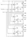
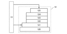
<バックライト12の構成例>
図9は、面発光を行うバックライト12の構成例を示す図である。図9に示すバックライト12は、基板120と、基板120上に設けられた電極層121と、電極層121上に設けられた有機物層122と、有機物層122上に設けられた中間層123と、中間層123上に設けられた有機物層124と、有機物層124上に設けられた電極層125とを有する。なお、電極層121及び電極層125の電位は、制御回路13によって制御される。そして、該制御回路13によって、電極層121及び電極層125に電圧を印加することでバックライト12において発光が行われる。すなわち、図9に示すバックライト12は、電圧が印加されることによって発光する有機物を発光体として利用したバックライトである(いわゆる、有機EL(エレクトロルミネッセンス)を利用したバックライトである)。
<Configuration Example of
FIG. 9 is a diagram illustrating a configuration example of the
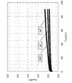
なお、図9に示すバックライト12は、電圧の印加によって図10に示す発光スペクトルを有する光を発光することが可能である。図10に示すように、図9に示したバックライト12が発光する光の発光スペクトルは、2つのピークを有する。具体的には、当該発光スペクトルは、青色(B)の波長領域(400nm以上480nm未満)及び黄色(Y)の波長領域(560nm以上580nm未満)にピークを有し且つ黄色(Y)の波長領域のピークの方が青色(B)の波長領域のピークよりも高い。これらのピークは、それぞれ異なる有機物層の発光に起因している。すなわち、有機物層122に電圧が印加されることによって当該2つのピークの一方に対応する発光スペクトルを有する光を発光し、且つ有機物層124に電圧が印加されることによって当該2つのピークの他方に対応する発光スペクトルを有する光を発光する。これにより、図9に示すバックライト12が、図10に示す発光スペクトルを有する光を発光することが可能になる。なお、青色(B)と黄色(Y)は補色の関係になり、図10に示す発光スペクトルを有する光は白色光である。
Note that the
なお、白色光を形成するための光の組み合わせは、複数存在する。例えば、青緑色を呈する光と赤色を呈する光を混色すること、又は淡青(スカイブルー)色を呈する光と朱色を呈する光を混色することなどによって白色光を形成することが可能である。ただし、青色(B)を呈する光と、該青色(B)を呈する光よりも発光強度の高い黄色(Y)を呈する光とを混色して白色光を形成する場合、電力効率を高めること(消費電極を低減すること)が可能であり好ましい。なぜなら、人の目は、波長が555nmの光に対する視感度が最も高く、且つ波長が555nmから離れるに従って光の視感度が低下する。すなわち、光子数が同じ場合、555nmの波長を有する光が最も強い光として人に視認される。そのため、波長が555nmに近い黄色(Y)を呈する光を白色光の形成に用いることで、効率よく視感度の高い白色光を形成することが可能である。 There are a plurality of combinations of light for forming white light. For example, white light can be formed by mixing light exhibiting blue green and light exhibiting red, or mixing light exhibiting light blue (sky blue) and light exhibiting vermilion. However, when the white light is formed by mixing light exhibiting blue (B) and light exhibiting yellow (Y) having a higher emission intensity than the light exhibiting blue (B), power efficiency is increased ( It is possible and preferable to reduce the consumption electrode). This is because the human eye has the highest visibility for light having a wavelength of 555 nm, and the visibility of light decreases as the wavelength moves away from 555 nm. That is, when the number of photons is the same, light having a wavelength of 555 nm is visually recognized as the strongest light. Therefore, it is possible to efficiently form white light with high visibility by using light exhibiting yellow (Y) with a wavelength close to 555 nm for forming white light.
なお、上述した液晶表示装置においては、上記白色光が赤色(R)を呈する波長領域の光のみを透過するカラーフィルター、緑色(G)を呈する波長領域の光のみを透過するカラーフィルター、又は青色(B)を呈する波長領域の光のみを透過するカラーフィルターを透過する。そのため、当該バックライトが発する光が、赤色(R)を呈する波長、緑色(G)を呈する波長、及び青色(B)を呈する波長の光を含む光であることが必要とされる。ここで、図9に示すバックライトが発する白色光は、有機ELを利用して形成される。一般に、有機ELを利用して形成される光の発光スペクトルは、ブロードなピークを示す。そのため、有機ELを利用して形成される黄色(Y)を呈する波長領域の光が、緑色(G)を呈する波長領域の光及び赤色(R)を呈する波長領域の光を含む。これにより、図9に示すバックライトは、上述した液晶表示装置におけるバックライトとして適用することが可能である。 In the liquid crystal display device described above, the white light is a color filter that transmits only light in the wavelength region that exhibits red (R), a color filter that transmits only light in the wavelength region that exhibits green (G), or blue. The color filter that transmits only light in the wavelength region exhibiting (B) is transmitted. Therefore, the light emitted from the backlight is required to include light having a wavelength exhibiting red (R), a wavelength exhibiting green (G), and a wavelength exhibiting blue (B). Here, the white light emitted from the backlight shown in FIG. 9 is formed using organic EL. In general, the emission spectrum of light formed using organic EL shows a broad peak. Therefore, the light in the wavelength region exhibiting yellow (Y) formed using the organic EL includes the light in the wavelength region exhibiting green (G) and the light in the wavelength region exhibiting red (R). Accordingly, the backlight shown in FIG. 9 can be applied as a backlight in the above-described liquid crystal display device.
以下では、図9に示すバックライト12の各構成要素に適用可能な材料について列挙する。なお、以下では、電極層121が陽極、有機物層122が黄色(Y)を呈する波長領域の光を発光することが可能な有機物、有機物層124が青色(B)を呈する波長領域の光を発光することが可能な有機物、電極層125が陰極として説明するが、これらの構成要素は適宜入れ替えることが可能である。
Below, materials applicable to each component of the
基板120は、支持体として用いられる。基板120としては、例えばガラス、またはプラスチックなどを用いることができる。なお、電極層121、125、有機物層122、125、及び中間層123の作製工程において支持体として機能するものであれば、これら以外のものでもよい。
The
電極層121、125には、様々な金属、合金、その他の導電性材料、およびこれらの混合物などを用いることができる。例えば、仕事関数の大きい材料である、酸化インジウム−酸化スズ(ITO:Indium Tin Oxide)、珪素または酸化珪素を含有した酸化インジウム−酸化スズ、酸化インジウム−酸化亜鉛(IZO:Indium Zinc Oxide)、酸化タングステン及び酸化亜鉛を含有した酸化インジウム(IWZO)等の導電性を有する金属酸化物膜を用いることができる。これらの金属酸化物膜は、スパッタリング法により形成することができる。または、ゾル−ゲル法などを用いて形成することができる。例えば、酸化インジウム−酸化亜鉛(IZO)は、酸化インジウムに対し1〜20wt%の酸化亜鉛を加えたターゲットを用いてスパッタリング法により形成することができる。また、酸化タングステン及び酸化亜鉛を含有した酸化インジウム(IWZO)は、酸化インジウムに対し酸化タングステンを0.5〜5wt%、酸化亜鉛を0.1〜1wt%含有したターゲットを用いてスパッタリング法により形成することができる。この他、金(Au)、白金(Pt)、ニッケル(Ni)、タングステン(W)、クロム(Cr)、モリブデン(Mo)、鉄(Fe)、コバルト(Co)、銅(Cu)、パラジウム(Pd)、または金属材料の窒化物(例えば、窒化チタン)等を用いることができる。また、仕事関数の小さい材料である、元素周期表の第1族または第2族に属する元素、すなわちリチウム(Li)、セシウム(Cs)等のアルカリ金属、マグネシウム(Mg)、カルシウム(Ca)、ストロンチウム(Sr)等のアルカリ土類金属、またはこれらを含む合金(マグネシウムと銀の合金、アルミニウムとリチウムの合金)を用いることができる。また、ユーロピウム(Eu)、イッテルビウム(Yb)等の希土類金属、またはこれらを含む合金等を用いることができる。また、アルミニウム(Al)、銀(Ag)、アルミニウムを含む合金(AlSi)等を用いることができる。アルカリ金属、アルカリ土類金属、またはこれらを含む合金の膜は、真空蒸着法を用いて形成することができる。また、アルカリ金属またはアルカリ土類金属を含む合金の膜はスパッタリング法により形成することも可能である。また、これらの電極は、単層膜に限らず、積層膜で形成することもできる。
For the electrode layers 121 and 125, various metals, alloys, other conductive materials, a mixture thereof, and the like can be used. For example, indium oxide-tin oxide (ITO), indium oxide-tin oxide containing silicon or silicon oxide, indium zinc-oxide (IZO), oxidation, which are materials having a high work function. A conductive metal oxide film such as indium oxide (IWZO) containing tungsten and zinc oxide can be used. These metal oxide films can be formed by a sputtering method. Alternatively, it can be formed using a sol-gel method or the like. For example, indium oxide-zinc oxide (IZO) can be formed by a sputtering method using a target in which 1 to 20 wt% of zinc oxide is added to indium oxide. Indium oxide containing tungsten oxide and zinc oxide (IWZO) is formed by sputtering using a target containing 0.5 to 5 wt% tungsten oxide and 0.1 to 1 wt% zinc oxide with respect to indium oxide. can do. In addition, gold (Au), platinum (Pt), nickel (Ni), tungsten (W), chromium (Cr), molybdenum (Mo), iron (Fe), cobalt (Co), copper (Cu), palladium ( Pd), a nitride of a metal material (for example, titanium nitride), or the like can be used. In addition, an element belonging to
なお、キャリアの注入障壁を考慮すると、陽極として機能する電極層121は、仕事関数の大きい材料を用いることが好ましい。また、陰極として機能する電極層125は、仕事関数の小さい材料を用いることが好ましい。
In consideration of a carrier injection barrier, the
有機物層122は、黄色(Y)の波長領域にピークを有する発光性の物質を有している。黄色(Y)の波長領域にピークを有する発光性の物質として、ルブレン、(2−{2−[4−(ジメチルアミノ)フェニル]エテニル}−6−メチル−4H−ピラン−4−イリデン)プロパンジニトリル(略称:DCM1)、{2−メチル−6−[2−(2,3,6,7−テトラヒドロ−1H,5H−ベンゾ[ij]キノリジン−9−イル)エテニル]−4H−ピラン−4−イリデン}プロパンジニトリル(略称:DCM2)、ビス[2−(2−チエニル)ピリジナト]イリジウムアセチルアセトナート(Ir(thp)2(acac))、ビス(2−フェニルキノリナト)イリジウムアセチルアセトナート(Ir(pq)2(acac))、トリス(2−フェニルキノリナト−N,C2’)イリジウム(III)(略称:Ir(pq)3)、ビス(2−フェニルベンゾチアゾラト−N,C2’)イリジウム(III)アセチルアセトナート(略称:Ir(bt)2(acac))、(アセチルアセトナト)ビス[2,3−ビス(4−フルオロフェニル)−5−メチルピラジナト]イリジウム(III)(略称:Ir(Fdppr−Me)2(acac))、(アセチルアセトナト)ビス{2−(4−メトキシフェニル)−3,5−ジメチルピラジナト}イリジウム(III)(略称:Ir(dmmoppr)2(acac))、(アセチルアセトナト)ビス(3,5−ジメチル−2−フェニルピラジナト)イリジウム(III)(略称:Ir(mppr−Me)2(acac))、(アセチルアセトナト)ビス(5−イソプロピル−3−メチル−2−フェニルピラジナト)イリジウム(III)(略称:Ir(mppr−iPr)2(acac))などを用いることができる。また、黄色(Y)の波長領域にピークを有する発光性の物質としては、Ir(thp)2(acac)、Ir(pq)2(acac)、Ir(pq)3、Ir(bt)2(acac)、Ir(Fdppr−Me)2(acac)、Ir(dmmoppr)2(acac)、Ir(mppr−Me)2(acac)、Ir(mppr−iPr)2(acac)のような燐光性化合物が好ましい。燐光性化合物を用いることにより、蛍光性化合物を用いた場合と比べて電力効率を3〜4倍高めることができる。なお、黄色(Y)の燐光性化合物を用いた素子は、青色(B)の燐光性化合物を用いた素子に比べ、長寿命が得やすい。特に、Ir(Fdppr−Me)2(acac)、Ir(dmmoppr)2(acac)、Ir(mppr−Me)2(acac)、Ir(mppr−iPr)2(acac)のようなピラジン誘導体を配位子とする有機金属錯体が、高効率であるため好ましい。また、これらの発光性の物質(ゲスト材料)を他の物質(ホスト材料)に分散させることにより、発光層を構成しても良い。この場合のホスト材料としては、4,4’−ビス[N−(1−ナフチル)−N−フェニルアミノ]ビフェニル(略称:NPB)や4−(9H−カルバゾール−9−イル)−4’−(10−フェニル−9−アントリル)トリフェニルアミン(略称:YGAPA)などの芳香族アミン化合物や、2−[4−(9H−カルバゾール−9−イル)フェニル]−3−フェニルキノキサリン(略称:Cz1PQ)、2−[4−(3,6−ジフェニル−9H−カルバゾール−9−イル)フェニル]−3−フェニルキノキサリン(略称:Cz1PQ−III)、2−[4−(3,6−ジフェニル−9H−カルバゾール−9−イル)フェニル]ジベンゾ[f,h]キノキサリン(略称:2CzPDBq−III)、2−[3−(ジベンゾチオフェン−4−イル)フェニル]ジベンゾ[f,h]キノキサリン(略称:2mDBTPDBq−II)のような複素環化合物が好適である。また、ポリ(2,5−ジアルコキシ−1,4−フェニレンビニレン)等のポリマーを用いても良い。
The
中間層123は、有機物層122に対して電子を注入する機能を有し、且つ有機物層124に対して正孔を注入する機能を有する。したがって、中間層123は、少なくとも正孔を注入する機能を有する層と電子を注入する機能を有する層とを積層した積層膜を用いることができる。また、中間層123は、有機物層122、124の内部に位置する層であるため、光の取り出し効率の点から、透光性を有する材料を用いることが好ましい。また、中間層123のうちの一部は、電極層121、125に用いる材料と同じ材料を用いて形成すること、または、電極層121、125よりも導電率の低い材料を用いて形成することが可能である。中間層123のうち電子を注入する機能を有する層として、例えば、酸化リチウム、フッ化リチウム、炭酸セシウム、または、電子輸送性の高い物質に、ドナー性物質を添加した材料を用いることができる。
The
電子輸送性の高い物質としては、例えば、トリス(8−キノリノラト)アルミニウム(略称:Alq)、トリス(4−メチル−8−キノリノラト)アルミニウム(略称:Almq3)、ビス(10−ヒドロキシベンゾ[h]キノリナト)ベリリウム(略称:BeBq2)、ビス(2−メチル−8−キノリノラト)(4−フェニルフェノラト)アルミニウム(略称:BAlq)などのキノリン骨格またはベンゾキノリン骨格を有する金属錯体等を用いることができる。また、この他に、ビス[2−(2−ヒドロキシフェニル)ベンゾオキサゾラト]亜鉛(略称:Zn(BOX)2)、ビス[2−(2−ヒドロキシフェニル)ベンゾチアゾラト]亜鉛(略称:Zn(BTZ)2)などのオキサゾール系、チアゾール系配位子を有する金属錯体なども用いることができる。また、金属錯体以外にも、2−(4−ビフェニリル)−5−(4−tert−ブチルフェニル)−1,3,4−オキサジアゾール(略称:PBD)、1,3−ビス[5−(p−tert−ブチルフェニル)−1,3,4−オキサジアゾール−2−イル]ベンゼン(略称:OXD−7)、3−(4−ビフェニリル)−4−フェニル−5−(4−tert−ブチルフェニル)−1,2,4−トリアゾール(略称:TAZ)、バソフェナントロリン(略称:BPhen)、バソキュプロイン(略称:BCP)なども用いることができる。ここに挙げた物質は、主に10−6cm2/Vs以上の電子移動度を有する物質である。なお、正孔よりも電子の輸送性の高い物質であれば、上記以外の物質を用いることも可能である。 Examples of the substance having a high electron transporting property include tris (8-quinolinolato) aluminum (abbreviation: Alq), tris (4-methyl-8-quinolinolato) aluminum (abbreviation: Almq 3 ), and bis (10-hydroxybenzo [h ] A metal complex having a quinoline skeleton or a benzoquinoline skeleton, such as quinolinato) beryllium (abbreviation: BeBq 2 ), bis (2-methyl-8-quinolinolato) (4-phenylphenolato) aluminum (abbreviation: BAlq), or the like. Can do. In addition, bis [2- (2-hydroxyphenyl) benzoxazolate] zinc (abbreviation: Zn (BOX) 2 ), bis [2- (2-hydroxyphenyl) benzothiazolate] zinc (abbreviation: Zn ( A metal complex having an oxazole-based or thiazole-based ligand such as BTZ) 2 ) can also be used. In addition to metal complexes, 2- (4-biphenylyl) -5- (4-tert-butylphenyl) -1,3,4-oxadiazole (abbreviation: PBD), 1,3-bis [5- (P-tert-butylphenyl) -1,3,4-oxadiazol-2-yl] benzene (abbreviation: OXD-7), 3- (4-biphenylyl) -4-phenyl-5- (4-tert -Butylphenyl) -1,2,4-triazole (abbreviation: TAZ), bathophenanthroline (abbreviation: BPhen), bathocuproin (abbreviation: BCP), and the like can also be used. The substances mentioned here are mainly substances having an electron mobility of 10 −6 cm 2 / Vs or higher. Note that other than the above substances, any substance that has a property of transporting more electrons than holes can be used.
電子輸送性の高い物質に、ドナー性物質を添加することにより、電子注入性を高くすることができる。そのため、バックライトの駆動電圧を低減することができる。ドナー性物質としては、アルカリ金属またはアルカリ土類金属または希土類金属または元素周期表における第13族に属する金属またはその酸化物またはその炭酸塩を用いることができる。具体的には、リチウム(Li)、セシウム(Cs)、マグネシウム(Mg)、カルシウム(Ca)、イッテルビウム(Yb)、インジウム(In)、酸化リチウム、炭酸セシウムなどを用いることが好ましい。また、テトラチアナフタセンのような有機化合物をドナー性物質として用いてもよい。 By adding a donor substance to a substance having a high electron transporting property, the electron injecting property can be increased. Therefore, the driving voltage of the backlight can be reduced. As the donor substance, an alkali metal, an alkaline earth metal, a rare earth metal, a metal belonging to Group 13 of the periodic table, an oxide thereof, or a carbonate thereof can be used. Specifically, lithium (Li), cesium (Cs), magnesium (Mg), calcium (Ca), ytterbium (Yb), indium (In), lithium oxide, cesium carbonate, or the like is preferably used. Further, an organic compound such as tetrathianaphthacene may be used as a donor substance.
また、中間層123のうち正孔を注入する機能を有する層として、例えば、酸化モリブデン、酸化バナジウム、酸化レニウム、酸化ルテニウム等を用いること、または、正孔輸送性の高い物質に、アクセプター物質を添加した材料を用いることができる。また、アクセプター物質からなる層を用いても良い。
As the layer having a function of injecting holes in the
正孔輸送性の高い物質としては、例えば、4,4’−ビス[N−(1−ナフチル)−N−フェニルアミノ]ビフェニル(略称:NPB)、N,N’−ビス(3−メチルフェニル)−N,N’−ジフェニル−[1,1’−ビフェニル]−4,4’−ジアミン(略称:TPD)、4,4’,4’’−トリス(N,N−ジフェニルアミノ)トリフェニルアミン(略称:TDATA)、4,4’,4’’−トリス[N−(3−メチルフェニル)−N−フェニルアミノ]トリフェニルアミン(略称:MTDATA)、4,4’−ビス[N−(スピロ−9,9’−ビフルオレン−2−イル)−N−フェニルアミノ]−1,1’−ビフェニル(略称:BSPB)などの芳香族アミン化合物等を用いることができる。ここに挙げた物質は、主に10−6cm2/Vs以上の正孔移動度を有する物質である。但し、電子よりも正孔の輸送性の高い物質であれば、上記以外の物質を用いても構わない。また、上述のホスト材料を用いてもよい。 As a substance having a high hole-transport property, for example, 4,4′-bis [N- (1-naphthyl) -N-phenylamino] biphenyl (abbreviation: NPB), N, N′-bis (3-methylphenyl) ) -N, N′-diphenyl- [1,1′-biphenyl] -4,4′-diamine (abbreviation: TPD), 4,4 ′, 4 ″ -tris (N, N-diphenylamino) triphenyl Amine (abbreviation: TDATA), 4,4 ′, 4 ″ -tris [N- (3-methylphenyl) -N-phenylamino] triphenylamine (abbreviation: MTDATA), 4,4′-bis [N— An aromatic amine compound such as (spiro-9,9′-bifluoren-2-yl) -N-phenylamino] -1,1′-biphenyl (abbreviation: BSPB) can be used. The substances mentioned here are mainly substances having a hole mobility of 10 −6 cm 2 / Vs or higher. Note that other than the above substances, any substance that has a property of transporting more holes than electrons may be used. Further, the above host material may be used.
正孔輸送性の高い物質に、アクセプター性物質を添加することにより、正孔注入性を高くすることができる。そのため、発光素子の駆動電圧を低減することができる。アクセプター性物質としては、7,7,8,8−テトラシアノ−2,3,5,6−テトラフルオロキノジメタン(略称:F4−TCNQ)、クロラニル等を用いることができる。また、遷移金属酸化物を用いることができる。また元素周期表における第4族乃至第8族に属する金属の酸化物を用いることができる。具体的には、酸化バナジウム、酸化ニオブ、酸化タンタル、酸化クロム、酸化モリブデン、酸化タングステン、酸化マンガン、酸化レニウムは電子受容性が高いため好ましい。特に、酸化モリブデンは大気中でも安定であり、吸湿性が低く、扱いやすいため好ましい。 By adding an acceptor substance to a substance having a high hole transporting property, the hole injecting property can be increased. Therefore, the driving voltage of the light emitting element can be reduced. As the acceptor substance, 7,7,8,8-tetracyano-2,3,5,6-tetrafluoroquinodimethane (abbreviation: F 4 -TCNQ), chloranil, or the like can be used. Transition metal oxides can also be used. Alternatively, an oxide of a metal belonging to Groups 4 to 8 in the periodic table can be used. Specifically, vanadium oxide, niobium oxide, tantalum oxide, chromium oxide, molybdenum oxide, tungsten oxide, manganese oxide, and rhenium oxide are preferable because of their high electron accepting properties. In particular, molybdenum oxide is preferable because it is stable in the air, has a low hygroscopic property, and is easy to handle.
また、正孔輸送性の高い物質にアクセプター性物質を添加した構成および電子輸送性の高い物質にドナー性物質を添加した構成のいずれか一方または両方の構成を用いることにより、中間層123を厚膜化しても、駆動電圧の上昇を抑制することができる。よって、中間層123を厚膜化することにより、微小な異物や衝撃等によるショートを防止することができ、信頼性の高いバックライトを得ることができる。
Further, by using one or both of a configuration in which an acceptor substance is added to a substance having a high hole-transport property and a donor substance is added to a substance having a high electron-transport property, the
なお、中間層において、正孔を注入する機能を有する層と電子を注入する機能を有する層との間に、必要に応じて他の層を導入しても良い。例えば、ITOのような導電層や電子リレー層を設けても良い。電子リレー層は、正孔を注入する機能を有する層と電子を注入する機能を有する層との間で生じる電圧のロスを低減する機能を有する。具体的には、LUMO準位がおよそ−5.0eV以上である材料を用いるのが好ましく、−5.0eV以上−3.0eV以下である材料を用いるのがより好ましい。例えば、3,4,9,10−ペリレンテトラカルボン酸二無水物(略称:PTCDA)、3,4,9,10−ペリレンテトラカルボキシリックビスベンゾイミダゾール(略称:PTCBI)などを用いることができる。 In the intermediate layer, another layer may be introduced between the layer having a function of injecting holes and the layer having a function of injecting electrons, if necessary. For example, a conductive layer such as ITO or an electronic relay layer may be provided. The electron relay layer has a function of reducing voltage loss generated between a layer having a function of injecting holes and a layer having a function of injecting electrons. Specifically, a material having an LUMO level of approximately −5.0 eV or more is preferably used, and a material having −5.0 eV or more and −3.0 eV or less is more preferably used. For example, 3,4,9,10-perylenetetracarboxylic dianhydride (abbreviation: PTCDA), 3,4,9,10-perylenetetracarboxylic bisbenzimidazole (abbreviation: PTCBI), or the like can be used.
有機物層124は、青色(B)の波長領域にピークを有する発光性の物質を有している。青色(B)の波長領域にピークを有する発光性の物質として、ペリレン、2,5,8,11−テトラ(tert−ブチル)ペリレン(略称:TBP)などを用いることができる。また、4,4’−ビス(2,2−ジフェニルビニル)ビフェニル(略称:DPVBi)などのスチリルアリーレン誘導体や、9,10−ジフェニルアントラセン、9,10−ジ(2−ナフチル)アントラセン(略称:DNA)、9,10−ビス(2−ナフチル)−2−tert−ブチルアントラセン(略称:t−BuDNA)などのアントラセン誘導体を用いることができる。また、ポリ(9,9−ジオクチルフルオレン)等のポリマーを用いることができる。また、N,N’−ビス[4−(9H−カルバゾール−9−イル)フェニル]−N,N’−ジフェニルスチルベン−4,4’−ジアミン(略称:YGA2S)や、N,N’−ジフェニル−N,N’−ビス(9−フェニル−9H−カルバゾール−3−イル)スチルベン−4,4’−ジアミン(略称:PCA2S)などのスチリルアミン誘導体を用いることができる。また、N,N’−ビス〔4−(9−フェニル−9H−フルオレン−9−イル)フェニル〕−N,N’−ジフェニルピレン−1,6−ジアミン(略称:1,6FLPAPrn)、N,N’−ビス〔4−(9−フェニル−9H−フルオレン−9−イル)フェニル〕−N,N’−ビス(4−tert−ブチルフェニル)−ピレン−1,6−ジアミン(略称:1,6tBu−FLPAPrn)のようなピレンジアミン誘導体を用いることができる。また、青色の波長領域にピークを有する発光性の物質としては、蛍光性化合物を用いることが好ましい。青色(B)の発光性の物質として蛍光性化合物を用いることにより、青色(B)の発光性の物質として燐光性化合物を用いた場合と比べて長寿命の発光素子を得ることができる。特に1,6FLPAPrn、1,6tBu−FLPAPrnのようなピレンジアミン誘導体は、460nm付近にピークを有している上に、極めて高い量子収率が得られ、長寿命であるため好ましい。また、これらの発光性の物質(ゲスト材料)を他の物質(ホスト材料)に分散させることにより、発光層を構成しても良い。この場合のホスト材料としては、アントラセン誘導体が好ましく、9,10−ビス(2−ナフチル)−2−tert−ブチルアントラセン(略称:t−BuDNA)、9−[4−(10−フェニル−9−アントリル)フェニル]−9H−カルバゾール(略称:CzPA)、9−フェニル−3−[4−(10−フェニル−9−アントリル)フェニル]−9H−カルバゾール(略称:PCzPA)などが好適である。特に、CzPAやPCzPAは電気化学的に安定であるため好ましい。
The
<制御回路13の構成例>
図11は、制御回路13の構成例を示す図である。図11に示す制御回路13は、信号生成回路130と、記憶回路131と、比較回路132と、選択回路133と、出力制御回路134とを有する。
<Configuration Example of
FIG. 11 is a diagram illustrating a configuration example of the
信号生成回路130は、表示パネル11を動作させ、画素部に画像を形成するための信号、及びバックライト12を発光させるための駆動電圧を生成する回路である。なお、前者は、画素部にマトリクス状に配設された複数の画素に対して入力される画像信号(Data)、走査線駆動回路111又は信号線駆動回路112の動作を制御する信号(例えば、スタートパルス信号(SP)、クロック信号(CK)など)、並びに駆動回路用の電源電圧である高電源電位(Vdd)及び低電源電位(Vss)などを指す。なお、図11に示す制御回路13においては、信号生成回路130は、記憶回路131に対して画像信号(Data)を出力し、出力制御回路134に対して表示パネル11(走査線駆動回路111及び信号線駆動回路112)の動作を制御する信号及びバックライト12を発光させるための駆動電圧を出力する。また、信号生成回路130から記憶回路131に対して出力される画像信号(Data)がアナログ信号である場合には、A/Dコンバータなどを介して、当該画像信号(Data)をデジタル信号に変換することもできる。
The
記憶回路131は、画素部において、第1の画像を形成するための画像信号乃至第nの画像(nは、2以上の自然数)を形成するための画像信号を記憶するための複数のメモリ1310を有する。なお、メモリ1310は、DRAM(Dynamic Random Access Memory)、SRAM(Static Random Access Memory)などの記憶素子を用いて構成すればよい。また、メモリ1310は、画素部において形成される画像毎に画像信号を記憶する構成であればよく、メモリ1310の数は、特定の数に限定されない。加えて、複数のメモリ1310が記憶する画像信号は、比較回路132及び選択回路133により選択的に読み出される。
The
比較回路132は、記憶回路131に記憶された第kの画像(kは、1以上n未満の自然数)を形成するための画像信号及び第(k+1)の画像を形成するための画像信号を選択的に読み出して、当該画像信号の比較を行い、差分を検出する回路である。なお、第kの画像及び第(k+1)の画像は、画素部において連続して表示される画像である。比較回路132での画像信号の比較により、差分が検出された場合、当該画像信号によって形成される2枚の画像は動画であると判断される。一方、比較回路132での画像信号の比較により、差分が検出されない場合、当該画像信号によって形成される2枚の画像は静止画であると判断される。すなわち、比較回路132は、差分の検出によって連続して表示される画像を形成するための画像信号が、動画を表示するための画像信号であるか、静止画を表示するための画像信号であるかを判断する回路である。なお、比較回路132は、当該差分が一定のレベルを超えたときに、差分を検出したと判断されるように設定してもよい。
The
選択回路133は、比較回路132で検出された差分を基に、表示パネル11への画像信号の出力を選択する回路である。具体的には、選択回路133は、比較回路132で、差分が検出された画像を形成するための画像信号は出力し、差分が検出されない画像を形成するための画像信号は出力しない回路である。
The
出力制御回路134は、スタートパルス信号(SP)、クロック信号(CK)、高電源電位(Vdd)、及び低電源電位(Vss)などの制御信号の表示パネル11(走査線駆動回路111及び信号線駆動回路112)への供給を制御する回路である。具体的には、比較回路132により動画と判断された場合(連続して表示される画像に差分が検出された場合)には、選択回路133から供給された画像信号(Data)を信号線駆動回路112に出力するとともに、表示パネル11(走査線駆動回路111及び信号線駆動回路112)に対して、制御信号(スタートパルス信号(SP)、クロック信号(CK)、高電源電位(Vdd)、及び低電源電位(Vss)など)を供給する。一方、比較回路132により静止画と判断された場合(連続して表示される画像に差分が検出されない場合)には、選択回路133から画像信号(Data)が供給されないとともに、表示パネル11(走査線駆動回路111及び信号線駆動回路112)に対して、制御信号(スタートパルス信号(SP)、クロック信号(CK)、高電源電位(Vdd)、及び低電源電位(Vss)など)を供給しない。すなわち、比較回路132により静止画と判断された場合(連続して表示される画像に差分が検出されない場合)には、表示パネル11(走査線駆動回路111及び信号線駆動回路112)の動作を完全に停止させる。また、出力制御回路134は、表示パネル11に対して信号などを供給するか否かに関わらず、バックライト12に対してバックライト12を発光させるための駆動電圧の供給を行う。
The
また、上述した出力制御回路134において、静止画と判断される期間が短い場合には、高電源電位(Vdd)及び低電源電位(Vss)を供給し続ける構成とすることもできる。なお、高電源電位(Vdd)及び低電源電位(Vss)が供給されるとは、ある配線の電位が高電源電位(Vdd)又は低電源電位(Vss)に固定されることである。すなわち、ある電位状態にある当該配線が、高電源電位(Vdd)又は低電源電位(Vss)に変化することになる。当該電位の変化には電力消費が伴う。そのため、頻繁に高電源電位(Vdd)及び低電源電位(Vss)の供給の停止及び再供給を行うことで、結果的に、消費電力が増大する可能性がある。そのような場合には、高電源電位(Vdd)及び低電源電位(Vss)を供給し続ける構成とすることが好ましい。なお、上述した説明において、信号を「供給しない」とは、当該信号を供給する配線において所定の電位とは異なる電位が供給される、又は当該配線が浮遊状態になることを指すこととする。
Further, in the above-described
なお、上述した制御回路13において、静止画と判断される期間が長い場合には、画素部において表示されている画像を書き換えるため(リフレッシュを行うため)に、表示パネル11に対して再度信号などを供給する構成とすることもできる。すなわち、画素部において静止画を表示する期間が設定した期間を超過した際に、画素部において当該静止画を表示させるための画像信号などを再度表示パネル11に対して供給する構成とすることもできる。
In the above-described
<本明細書で開示される液晶表示装置について>
本明細書で開示される液晶表示装置は、表示パネルにおいて表示される画像に応じて、該表示パネルの動作を制御することが可能である。具体的には、当該表示パネルに配設された画素に対する画像信号の入力などを制御することが可能である。例えば、画素に対する画像信号の入力頻度を低減することで、当該液晶表示装置の消費電力を低減することが可能である。ここで、画素に対する画像信号の入力頻度を低減するということは、当該画素内に画像信号を保持したまま、画像信号の入力を制御するトランジスタがオフ状態を維持する期間が長期化するということである。そのため、従来の液晶表示装置においては、当該トランジスタのオフ電流が画素の表示に対して与える影響が顕在化する。具体的には、液晶素子に印加される電圧が低下し、当該液晶素子を有する画素の表示の劣化(変化)が顕在化する。なお、当該トランジスタのオフ電流は、トランジスタの動作温度の上昇に伴い増加する。そのため、発光に発熱を伴うバックライトを備える透過型の従来の液晶表示装置においては、消費電力と表示品質の間に強いトレードオフの関係が存在することになる。
<About the liquid crystal display device disclosed in the present specification>
The liquid crystal display device disclosed in this specification can control the operation of the display panel in accordance with an image displayed on the display panel. Specifically, it is possible to control input of an image signal to the pixels provided in the display panel. For example, the power consumption of the liquid crystal display device can be reduced by reducing the frequency of inputting image signals to the pixels. Here, reducing the input frequency of the image signal to the pixel means that the period during which the transistor that controls the input of the image signal is kept off while the image signal is held in the pixel is prolonged. is there. Therefore, in the conventional liquid crystal display device, the influence of the off-state current of the transistor on the display of the pixel becomes obvious. Specifically, the voltage applied to the liquid crystal element is decreased, and display deterioration (change) of a pixel including the liquid crystal element becomes obvious. Note that the off-state current of the transistor increases as the operating temperature of the transistor increases. For this reason, in a transmissive conventional liquid crystal display device having a backlight that emits heat when light is emitted, there is a strong trade-off relationship between power consumption and display quality.
これに対して、本明細書で開示される液晶表示装置は、バックライトとして面発光を行う光源を適用する。当該光源は、発光を面状に行う光源であるため発光面積が広い。そのため、当該バックライトでは、放熱を効率よく行うことができる。すなわち、当該バックライトは、発光時における温度上昇が抑制されたバックライトである。これに付随して、当該液晶表示装置においては、各画素に設けられるトランジスタの動作温度の上昇を抑制することが可能である。そのため、当該液晶表示装置においては、当該トランジスタのオフ電流の増加を抑制することが可能である。 On the other hand, the liquid crystal display device disclosed in this specification uses a light source that emits surface light as a backlight. Since the light source is a light source that emits light in a planar shape, the light emission area is wide. Therefore, the backlight can efficiently dissipate heat. That is, the backlight is a backlight in which a temperature rise during light emission is suppressed. Accompanying this, in the liquid crystal display device, it is possible to suppress an increase in the operating temperature of the transistor provided in each pixel. Therefore, in the liquid crystal display device, an increase in off-state current of the transistor can be suppressed.
さらに、上述した液晶表示装置は、各画素に設けられるトランジスタとして酸化物半導体層によってチャネル形成領域が構成されるトランジスタを適用する。当該酸化物半導体層は、高純度化されることで、導電型が限りなく真性型に近づく。そのため、当該酸化物半導体層では、熱励起に起因するキャリアの発生を抑制することができる。その結果、当該酸化物半導体層によってチャネル形成領域が構成されたトランジスタの動作温度の上昇に伴うオフ電流の増加を低減することができる。すなわち、当該トランジスタは、動作温度の上昇に伴うオフ電流値の増加が著しく小さいトランジスタである。そのため、当該液晶表示装置においては、バックライトの発光に伴い当該トランジスタの動作温度が上昇する場合であっても、表示品質の低下を抑制することが可能である。 Further, in the above liquid crystal display device, a transistor in which a channel formation region is formed using an oxide semiconductor layer is used as a transistor provided in each pixel. When the oxide semiconductor layer is highly purified, the conductivity type is as close as possible to the intrinsic type. Therefore, in the oxide semiconductor layer, generation of carriers due to thermal excitation can be suppressed. As a result, an increase in off-state current accompanying an increase in operating temperature of a transistor in which a channel formation region is formed using the oxide semiconductor layer can be reduced. That is, the transistor is a transistor in which an increase in off-state current value with an increase in operating temperature is extremely small. Therefore, in the liquid crystal display device, it is possible to suppress deterioration in display quality even when the operating temperature of the transistor is increased with light emission of the backlight.
上述したように本発明の一態様の液晶表示装置は、バックライトとして放熱性に優れる光源を適用する。これにより、画素に対して長期間に渡って画像信号の入力が行われない場合であっても、当該画素において画像信号を保持することが可能になる。すなわち、消費電力の低減と表示品質の低下の抑制を両立することが可能になる。 As described above, the liquid crystal display device of one embodiment of the present invention employs a light source with excellent heat dissipation as a backlight. Accordingly, even when an image signal is not input to the pixel for a long period of time, the image signal can be held in the pixel. That is, it becomes possible to achieve both reduction of power consumption and suppression of deterioration of display quality.
<変形例>
上述した構成を有する液晶表示装置は、本発明の一態様であり、当該液晶表示装置と異なる点を有する液晶表示装置も本発明には含まれる。
<Modification>
The liquid crystal display device having the above structure is one embodiment of the present invention, and a liquid crystal display device having a different point from the liquid crystal display device is also included in the present invention.
<表示パネルの変形例>
例えば、上述した液晶表示装置においては、表示パネルの画素部においてマトリクス状に配設された複数の画素の各々に、特定色を呈する波長の光のみを透過するカラーフィルターが設けられる構成(図1(A)参照)について示したが、当該複数の画素の一部にカラーフィルターを設けない構成とすることが可能である。すなわち、上述した液晶表示装置においては、赤色(R)、緑色(G)、及び青色(B)の3色を用いて表示を行う構成について示したが、当該液晶表示装置が赤色(R)、緑色(G)、青色(B)、及び白色(W)の4色を用いて表示を行う構成とすることが可能である。この場合、液晶表示装置における白色表示に際のカラーフィルターによる光の減衰が生じないため、輝度を向上させること又は消費電力を低減することが可能である。
<Modification of display panel>
For example, in the liquid crystal display device described above, a configuration is provided in which each of a plurality of pixels arranged in a matrix in a pixel portion of a display panel is provided with a color filter that transmits only light having a wavelength exhibiting a specific color (FIG. 1). (A) is described, but a color filter may not be provided in some of the plurality of pixels. That is, in the above-described liquid crystal display device, a configuration in which display is performed using three colors of red (R), green (G), and blue (B) is shown. However, the liquid crystal display device is red (R), It is possible to adopt a configuration in which display is performed using four colors of green (G), blue (B), and white (W). In this case, since the light is not attenuated by the color filter at the time of white display in the liquid crystal display device, the luminance can be improved or the power consumption can be reduced.
また、上述した液晶表示装置においては、各画素に設けられるトランジスタ11011として、チャネルエッチ型と呼ばれるボトムゲート構造のトランジスタを適用する構成(図2参照)について示したが、トランジスタの構成は、当該構成に限定されない。例えば、図12(A)〜(C)に示すトランジスタを適用することが可能である。
In the liquid crystal display device described above, a structure in which a bottom-gate transistor called a channel etch type is used as the
図12(A)に示すトランジスタ510は、チャネル保護型(チャネルストップ型ともいう)と呼ばれるボトムゲート構造の一つである。
A
トランジスタ510は、絶縁表面を有する基板220上に、ゲート層221、ゲート絶縁層222、酸化物半導体層223、酸化物半導体層223のチャネル形成領域を覆うチャネル保護層として機能する絶縁層511、ソース層224a、及びドレイン層224bを含む。また、ソース層224a、ドレイン層224b、及び絶縁層511を覆う保護絶縁層226が形成されている。
The
なお、絶縁層511としては、酸化シリコン、窒化シリコン、酸化窒化シリコン、窒化酸化シリコン、酸化アルミニウム、酸化タンタルなどの絶縁体を適用することができる。また、これらの材料の積層構造を適用することもできる。
Note that as the insulating
図12(B)示すトランジスタ520はボトムゲート型のトランジスタであり、絶縁表面を有する基板である基板220上に、ゲート層221、ゲート絶縁層222、ソース層224a、ドレイン層224b、及び酸化物半導体層223を含む。また、ソース層224a及びドレイン層224bを覆い、酸化物半導体層223に接する絶縁層225が設けられている。絶縁層225上にはさらに保護絶縁層226が形成されている。
A
トランジスタ520においては、ゲート絶縁層222は基板220及びゲート層221上に接して設けられ、ゲート絶縁層222上にソース層224a、ドレイン層224bが接して設けられている。そして、ゲート絶縁層222、及びソース層224a、ドレイン層224b上に酸化物半導体層223が設けられている。
In the
図12(C)に示すトランジスタ530は、トップゲート構造のトランジスタの一つである。トランジスタ530は、絶縁表面を有する基板220上に、絶縁層531、酸化物半導体層223、ソース層224a、及びドレイン層224b、ゲート絶縁層222、ゲート層221を含み、ソース層224a、ドレイン層224bにそれぞれ配線層532a、配線層532bが接して設けられ電気的に接続している。
A
なお、絶縁層531としては、酸化シリコン、窒化シリコン、酸化窒化シリコン、窒化酸化シリコン、酸化アルミニウム、酸化タンタルなどの絶縁体を適用することができる。また、これらの材料の積層構造を適用することもできる。
Note that as the insulating
また、配線層532a、配線層532bとしては、アルミニウム(Al)、銅(Cu)、チタン(Ti)、タンタル(Ta)、タングステン(W)、モリブデン(Mo)、クロム(Cr)、ネオジム(Nd)、スカンジウム(Sc)から選ばれた元素、上述した元素を成分とする合金、または上述した元素を成分とする窒化物を適用することができる。また、これらの材料の積層構造を適用することもできる。
As the
<バックライトの変形例>
また、上述した液晶表示装置においては、バックライトとして青色(B)を発光することが可能な有機物及び黄色(Y)を発光することが可能な有機物を利用する構成(図9参照)について示したが、バックライトの構成は、当該構成に限定されない。例えば、当該バックライトが、n層(nは、3以上の自然数)の有機物層を有する構成とすることが可能である。具体的には、当該バックライトを図13に示す構成とすることなどが可能である。図13に示すバックライト12は、基板1200と、基板1200上に設けられた電極層1201と、電極層1201上に設けられた有機物層1202と、有機物層1202上に設けられた中間層1203と、中間層1203上に設けられた有機物層1204と、有機物層1204上に設けられた中間層1205と、中間層1205上に設けられた有機物層1206と、有機物層1206上に設けられた電極層1207とを有する。なお、電極層1201及び電極層1207の電位は、制御回路13によって制御される。そして、該制御回路13によって、電極層1201及び電極層1207に電圧を印加することで有機物層1202、1204、1206のそれぞれから発光させることで白色光を形成することが可能である。例えば、有機物層1202、1204、1206のそれぞれにおいて、赤色(R)、緑色(G)、及び青色(B)のいずれか且つ他の2層の有機物層と異なる色を呈する波長領域の光を発光すること、又は有機物層1202、1204、1206のいずれかにおいて、青色(B)を呈する波長領域の光を発光し、且つ他の2層の有機物層において、黄色(Y)を呈する波長領域の光を発光すること、によって白色光を形成することが可能である。なお、上述した液晶表示装置においては、表示パネル11に赤色(R)、緑色(G)、及び青色(B)を呈する波長領域の光のみを透過するカラーフィルターが配設される。そのため、バックライト12が発光する白色光が、赤色(R)、緑色(G)、及び青色(B)の混色によって形成される場合、表示パネル11において表示される赤色(R)及び緑色(G)の色純度を向上させることが可能である。すなわち、液晶表示装置における画質を向上させることが可能である。
<Modified example of backlight>
In the above-described liquid crystal display device, a structure using an organic substance capable of emitting blue (B) and an organic substance capable of emitting yellow (Y) as a backlight (see FIG. 9) is shown. However, the configuration of the backlight is not limited to the configuration. For example, the backlight can have an n-layer (n is a natural number of 3 or more) organic material layer. Specifically, the backlight can be configured as shown in FIG. The
赤色(R)を呈する波長領域の光を発光する有機物としては、N,N,N’,N’−テトラキス(4−メチルフェニル)テトラセン−5,11−ジアミン(略称:p−mPhTD)、7,14−ジフェニル−N,N,N’,N’−テトラキス(4−メチルフェニル)アセナフト[1,2−a]フルオランテン−3,10−ジアミン(略称:p−mPhAFD)、2−{2−イソプロピル−6−[2−(1,1,7,7−テトラメチル−2,3,6,7−テトラヒドロ−1H,5H−ベンゾ[ij]キノリジン−9−イル)エテニル]−4H−ピラン−4−イリデン}プロパンジニトリル(略称:DCJTI)、2−{2−tert−ブチル−6−[2−(1,1,7,7−テトラメチル−2,3,6,7−テトラヒドロ−1H,5H−ベンゾ[ij]キノリジン−9−イル)エテニル]−4H−ピラン−4−イリデン}プロパンジニトリル(略称:DCJTB)、2−(2,6−ビス{2−[4−(ジメチルアミノ)フェニル]エテニル}−4H−ピラン−4−イリデン)プロパンジニトリル(略称:BisDCM)、2−{2,6−ビス[2−(8−メトキシ−1,1,7,7−テトラメチル−2,3,6,7−テトラヒドロ−1H,5H−ベンゾ[ij]キノリジン−9−イル)エテニル]−4H−ピラン−4−イリデン}プロパンジニトリル(略称:BisDCJTM)などの蛍光性化合物、又はビス[2−(2’−ベンゾ[4,5−α]チエニル)ピリジナト−N,C3’]イリジウム(III)アセチルアセトナート(略称:Ir(btp)2(acac))、ビス(1−フェニルイソキノリナト−N,C2’)イリジウム(III)アセチルアセトナート(略称:Ir(piq)2(acac))、(アセチルアセトナト)ビス[2,3−ビス(4−フルオロフェニル)キノキサリナト]イリジウム(III)(略称:Ir(Fdpq)2(acac))、(アセチルアセトナト)ビス(2,3,5−トリフェニルピラジナト)イリジウム(III)(略称:Ir(tppr)2(acac))、2,3,7,8,12,13,17,18−オクタエチル−21H,23H−ポルフィリン白金(II)(略称:PtOEP)、トリス(1,3−ジフェニル−1,3−プロパンジオナト)(モノフェナントロリン)ユーロピウム(III)(略称:Eu(DBM)3(Phen))、トリス[1−(2−テノイル)−3,3,3−トリフルオロアセトナト](モノフェナントロリン)ユーロピウム(III)(略称:Eu(TTA)3(Phen))などの燐光性化合物が挙げられる。 As an organic substance that emits light in a wavelength region exhibiting red (R), N, N, N ′, N′-tetrakis (4-methylphenyl) tetracene-5,11-diamine (abbreviation: p-mPhTD), 7 , 14-diphenyl-N, N, N ′, N′-tetrakis (4-methylphenyl) acenaphtho [1,2-a] fluoranthene-3,10-diamine (abbreviation: p-mPhAFD), 2- {2- Isopropyl-6- [2- (1,1,7,7-tetramethyl-2,3,6,7-tetrahydro-1H, 5H-benzo [ij] quinolizin-9-yl) ethenyl] -4H-pyran- 4-Ilidene} propanedinitrile (abbreviation: DCJTI), 2- {2-tert-butyl-6- [2- (1,1,7,7-tetramethyl-2,3,6,7-tetrahydro-1H) , 5H-benzo [ij ] Quinolidine-9-yl) ethenyl] -4H-pyran-4-ylidene} propanedinitrile (abbreviation: DCJTB), 2- (2,6-bis {2- [4- (dimethylamino) phenyl] ethenyl}- 4H-pyran-4-ylidene) propanedinitrile (abbreviation: BisDCM), 2- {2,6-bis [2- (8-methoxy-1,1,7,7-tetramethyl-2,3,6, 7-tetrahydro-1H, 5H-benzo [ij] quinolizin-9-yl) ethenyl] -4H-pyran-4-ylidene} propanedinitrile (abbreviation: BisDCJTM), or bis [2- (2 '- benzo [4,5-α] thienyl) pyridinato -N, C 3'] iridium (III) acetylacetonate (abbreviation: Ir (btp) 2 (acac )), bis (1-Fe Ruisokinorinato -N, C 2 ') iridium (III) acetylacetonate (abbreviation: Ir (piq) 2 (acac )), ( acetylacetonato) bis [2,3-bis (4-fluorophenyl) quinoxalinato] iridium ( III) (abbreviation: Ir (Fdpq) 2 (acac)), (acetylacetonato) bis (2,3,5-triphenylpyrazinato) iridium (III) (abbreviation: Ir (tppr) 2 (acac)) 2,3,7,8,12,13,17,18-octaethyl-21H, 23H-porphyrin platinum (II) (abbreviation: PtOEP), tris (1,3-diphenyl-1,3-propanedionate) (monophenanthroline) europium (III) (abbreviation: Eu (DBM) 3 (Phen )), tris [1- (2-thenoyl -3,3,3-trifluoroacetonato] (monophenanthroline) europium (III) (abbreviation: Eu (TTA) 3 (Phen)) include a phosphorescent compound such.
また、緑色(G)を呈する波長領域の光を発光する有機物としては、クマリン30、N−(9,10−ジフェニル−2−アントリル)−N,9−ジフェニル−9H−カルバゾール−3−アミン(略称:2PCAPA)、N−[9,10−ビス(1,1’−ビフェニル−2−イル)−2−アントリル]−N,9−ジフェニル−9H−カルバゾール−3−アミン(略称:2PCABPhA)、N−(9,10−ジフェニル−2−アントリル)−N,N’,N’−トリフェニル−1,4−フェニレンジアミン(略称:2DPAPA)、N−[9,10−ビス(1,1’−ビフェニル−2−イル)−2−アントリル]−N,N’,N’−トリフェニル−1,4−フェニレンジアミン(略称:2DPABPhA)、9,10−ビス(1,1’−ビフェニル−2−イル)−N−[4−(9H−カルバゾール−9−イル)フェニル]−N−フェニルアントラセン−2−アミン(略称:2YGABPhA)、N,N,9−トリフェニルアントラセン−9−アミン(略称:DPhAPhA)、クマリン545T、N,N’−ジフェニルキナクリドン(略称:DPQd)などの蛍光性化合物、又はトリス(2−フェニルピリジナト)イリジウム(III)(略称:Ir(ppy)3)、ビス(2−フェニルピリジナト)イリジウム(III)アセチルアセトナート(略称:Ir(ppy)2(acac))、トリス(アセチルアセトナト)(モノフェナントロリン)テルビウム(III)(略称:Tb(acac)3(Phen))などの燐光性化合物が挙げられる。 Moreover, as an organic substance which emits light in a wavelength region exhibiting green (G), coumarin 30, N- (9,10-diphenyl-2-anthryl) -N, 9-diphenyl-9H-carbazol-3-amine ( Abbreviation: 2PCAPA), N- [9,10-bis (1,1′-biphenyl-2-yl) -2-anthryl] -N, 9-diphenyl-9H-carbazol-3-amine (abbreviation: 2PCABPhA), N- (9,10-diphenyl-2-anthryl) -N, N ′, N′-triphenyl-1,4-phenylenediamine (abbreviation: 2DPAPA), N- [9,10-bis (1,1 ′) -Biphenyl-2-yl) -2-anthryl] -N, N ′, N′-triphenyl-1,4-phenylenediamine (abbreviation: 2DPABPhA), 9,10-bis (1,1′-biphenyl-2) -B ) -N- [4- (9H-carbazol-9-yl) phenyl] -N-phenylanthracen-2-amine (abbreviation: 2YGABPhA), N, N, 9-triphenylanthracen-9-amine (abbreviation: DPhAPhA), coumarin 545T, fluorescent compounds such as N, N′-diphenylquinacridone (abbreviation: DPQd), or tris (2-phenylpyridinato) iridium (III) (abbreviation: Ir (ppy) 3 ), bis ( 2-phenylpyridinato) iridium (III) acetylacetonate (abbreviation: Ir (ppy) 2 (acac)), tris (acetylacetonato) (monophenanthroline) terbium (III) (abbreviation: Tb (acac) 3 ( Phen)) and the like.
また、青色(B)を呈する波長領域の光を発光する有機物は既出であるため、ここでは前述の説明を援用することとする。なお、基板1200は基板120と同じ材料を、電極層1201、1207は電極層121、125と同じ材料を、中間層1203、1205は中間層123と同じ材料を用いて構成することが可能である。
Moreover, since the organic substance which emits the light of the wavelength range which exhibits blue (B) has already been mentioned, suppose that the above-mentioned description is used here. Note that the
<制御回路13の変形例>
また、上述した液晶表示装置においては、制御回路が連続して表示される画像を比較し差分が検出されるか否かによって、表示パネルに対する信号などの供給を制御する構成(図11参照)について示したが、制御回路の構成は、当該構成に限定されない。例えば、外部から制御回路に対して入力される信号に応じて複数のモードの切り替えを行う構成とすることが可能である。
<Modification of
Further, in the above-described liquid crystal display device, the control circuit compares the images displayed in succession and controls the supply of signals and the like to the display panel depending on whether or not a difference is detected (see FIG. 11). Although shown, the configuration of the control circuit is not limited to this configuration. For example, a plurality of modes can be switched in accordance with a signal input to the control circuit from the outside.
具体的には、当該液晶表示装置に備え付けられた入力デバイスを利用者が操作することで、動画モード又は静止画モードを選択する構成とすることなどが可能である。ここで、動画モードとは、表示パネルにおける画像の書き換えを第1の周波数で行うモードであり、静止画モードとは、表示パネルにおける画像の書き換えを第1の周波数よりも低い第2の周波数で行うモードであるとする。すなわち、本明細書で開示される液晶表示装置には、液晶表示装置自体が自動的に画素に対する画像信号の入力頻度を制御することが可能な液晶表示装置のみならず、利用者が意図的に画素に対する画像信号の入力頻度を制御することが可能な液晶表示装置も含まれる。 Specifically, the user can operate the input device provided in the liquid crystal display device to select a moving image mode or a still image mode. Here, the moving image mode is a mode for rewriting an image on the display panel at a first frequency, and the still image mode is a mode for rewriting an image on the display panel at a second frequency lower than the first frequency. It is assumed that the mode is to be performed. That is, the liquid crystal display device disclosed in this specification includes not only a liquid crystal display device in which the liquid crystal display device itself can automatically control the input frequency of image signals to pixels, but also a user intentionally. A liquid crystal display device capable of controlling the frequency of inputting image signals to the pixels is also included.
また、当該液晶表示装置で表示される画像の種類に応じて、動画モード又は静止画モードが選択される構成とすることなどが可能である。例えば、画像信号の基となる電子データのファイル形式などを参照することにより、動画モード又は静止画モードが選択される構成とすることなどが可能である。 In addition, a moving image mode or a still image mode can be selected in accordance with the type of image displayed on the liquid crystal display device. For example, the moving image mode or the still image mode can be selected by referring to the file format of electronic data that is the basis of the image signal.
<液晶表示装置を搭載した各種電子機器について>
以下では、本明細書で開示される液晶表示装置を搭載した電子機器の例について図14を参照して説明する。
<About various electronic devices equipped with liquid crystal display devices>
Hereinafter, an example of an electronic device in which the liquid crystal display device disclosed in this specification is mounted will be described with reference to FIGS.
図14(A)は、ノート型のパーソナルコンピュータを示す図であり、本体2201、筐体2202、表示部2203、キーボード2204などによって構成されている。
FIG. 14A illustrates a laptop personal computer, which includes a
図14(B)は、携帯情報端末(PDA)を示す図であり、本体2211には表示部2213と、外部インターフェイス2215と、操作ボタン2214等が設けられている。また、操作用の付属品としてスタイラス2212がある。
FIG. 14B illustrates a personal digital assistant (PDA). A
図14(C)は、電子ペーパーの一例として、電子書籍2220を示す図である。電子書籍2220は、筐体2221および筐体2223の2つの筐体で構成されている。筐体2221および筐体2223は、軸部2237により一体とされており、該軸部2237を軸として開閉動作を行うことができる。このような構成により、電子書籍2220は、紙の書籍のように用いることが可能である。
FIG. 14C illustrates an
筐体2221には表示部2225が組み込まれ、筐体2223には表示部2227が組み込まれている。表示部2225および表示部2227は、続き画面を表示する構成としてもよいし、異なる画面を表示する構成としてもよい。異なる画面を表示する構成とすることで、例えば右側の表示部(図14(C)では表示部2225)に文章を表示し、左側の表示部(図14(C)では表示部2227)に画像を表示することができる。
A
また、図14(C)では、筐体2221に操作部などを備えた例を示している。例えば、筐体2221は、電源2231、操作キー2233、スピーカー2235などを備えている。操作キー2233により、頁を送ることができる。なお、筐体の表示部と同一面にキーボードやポインティングデバイスなどを備える構成としてもよい。また、筐体の裏面や側面に、外部接続用端子(イヤホン端子、USB端子、またはACアダプタおよびUSBケーブルなどの各種ケーブルと接続可能な端子など)、記録媒体挿入部などを備える構成としてもよい。さらに、電子書籍2220は、電子辞書としての機能を持たせた構成としてもよい。
FIG. 14C illustrates an example in which the
また、電子書籍2220は、無線で情報を送受信できる構成としてもよい。無線により、電子書籍サーバから、所望の書籍データなどを購入し、ダウンロードする構成とすることも可能である。
Further, the
なお、電子ペーパーは、情報を表示するものであればあらゆる分野に適用することが可能である。例えば、電子書籍以外にも、ポスター、電車などの乗り物の車内広告、クレジットカード等の各種カードにおける表示などに適用することができる。 Note that electronic paper can be applied to any field as long as it displays information. For example, in addition to electronic books, the present invention can be applied to posters, advertisements on vehicles such as trains, and displays on various cards such as credit cards.
図14(D)は、携帯電話機を示す図である。当該携帯電話機は、筐体2240および筐体2241の二つの筐体で構成されている。筐体2241は、表示パネル2242、スピーカー2243、マイクロフォン2244、ポインティングデバイス2246、カメラ用レンズ2247、外部接続端子2248などを備えている。また、筐体2240は、当該携帯電話機の充電を行う太陽電池セル2249、外部メモリスロット2250などを備えている。また、アンテナは筐体2241内部に内蔵されている。
FIG. 14D illustrates a mobile phone. The cellular phone includes two housings, a
表示パネル2242はタッチパネル機能を備えており、図14(D)には映像表示されている複数の操作キー2245を点線で示している。なお、当該携帯電話は、太陽電池セル2249から出力される電圧を各回路に必要な電圧に昇圧するための昇圧回路を実装している。また、上記構成に加えて、非接触ICチップ、小型記録装置などを内蔵した構成とすることもできる。
The
表示パネル2242は、使用形態に応じて表示の方向が適宜変化する。また、表示パネル2242と同一面上にカメラ用レンズ2247を備えているため、テレビ電話が可能である。スピーカー2243およびマイクロフォン2244は音声通話に限らず、テレビ電話、録音、再生などが可能である。さらに、筐体2240と筐体2241はスライドし、図14(D)のように展開している状態から重なり合った状態とすることができ、携帯に適した小型化が可能である。
In the
外部接続端子2248はACアダプタやUSBケーブルなどの各種ケーブルと接続可能であり、充電やデータ通信が可能になっている。また、外部メモリスロット2250に記録媒体を挿入し、より大量のデータの保存および移動に対応できる。また、上記機能に加えて、赤外線通信機能、テレビ受信機能などを備えたものであってもよい。
The
図14(E)は、デジタルカメラを示す図である。当該デジタルカメラは、本体2261、表示部(A)2267、接眼部2263、操作スイッチ2264、表示部(B)2265、バッテリー2266などによって構成されている。
FIG. 14E illustrates a digital camera. The digital camera includes a
図14(F)は、テレビジョン装置を示す図である。テレビジョン装置2270では、筐体2271に表示部2273が組み込まれている。表示部2273により、映像を表示することが可能である。なお、ここでは、スタンド2275により筐体2271を支持した構成を示している。
FIG. 14F illustrates a television device. In the
テレビジョン装置2270の操作は、筐体2271が備える操作スイッチや、別体のリモコン操作機2280により行うことができる。リモコン操作機2280が備える操作キー2279により、チャンネルや音量の操作を行うことができ、表示部2273に表示される映像を操作することができる。また、リモコン操作機2280に、当該リモコン操作機2280から出力する情報を表示する表示部2277を設ける構成としてもよい。
The
なお、テレビジョン装置2270は、受信機やモデムなどを備えた構成とするのが好適である。受信機により、一般のテレビ放送の受信を行うことができる。また、モデムを介して有線または無線による通信ネットワークに接続することにより、一方向(送信者から受信者)または双方向(送信者と受信者間、あるいは受信者間同士など)の情報通信を行うことが可能である。
Note that the
10A 偏光板
10B 偏光板
11 表示パネル
12 バックライト
13 制御回路
14A FPC(Flexible Printed Circuits)
14B FPC(Flexible Printed Circuits)
110 画素部
111 走査線駆動回路
112 信号線駆動回路
120 基板
121 電極層
122 有機物層
123 中間層
124 有機物層
125 電極層
130 信号生成回路
131 記憶回路
132 比較回路
133 選択回路
134 出力制御回路
220 基板
221 ゲート層
222 ゲート絶縁層
223 酸化物半導体層
224a ソース層
224b ドレイン層
225 絶縁層
226 保護絶縁層
510 トランジスタ
511 絶縁層
520 トランジスタ
530 トランジスタ
531 絶縁層
532a 配線層
532b 配線層
1101 画素
1102R カラーフィルター
1102G カラーフィルター
1102B カラーフィルター
1111 走査線
1121 信号線
1200 基板
1201 電極層
1202 有機物層
1203 中間層
1204 有機物層
1205 中間層
1206 有機物層
1207 電極層
1310 メモリ
1800 測定系
1802 容量素子
1804 トランジスタ
1805 トランジスタ
1806 トランジスタ
1808 トランジスタ
2201 本体
2202 筐体
2203 表示部
2204 キーボード
2211 本体
2212 スタイラス
2213 表示部
2214 操作ボタン
2215 外部インターフェイス
2220 電子書籍
2221 筐体
2223 筐体
2225 表示部
2227 表示部
2231 電源
2233 操作キー
2235 スピーカー
2237 軸部
2240 筐体
2241 筐体
2242 表示パネル
2243 スピーカー
2244 マイクロフォン
2245 操作キー
2246 ポインティングデバイス
2247 カメラ用レンズ
2248 外部接続端子
2249 太陽電池セル
2250 外部メモリスロット
2261 本体
2263 接眼部
2264 操作スイッチ
2265 表示部(B)
2266 バッテリー
2267 表示部(A)
2270 テレビジョン装置
2271 筐体
2273 表示部
2275 スタンド
2277 表示部
2279 操作キー
2280 リモコン操作機
11011 トランジスタ
11012 容量素子
11013 液晶素子
10A
14B FPC (Flexible Printed Circuits)
110
2266
2270
Claims (8)
前記画素部に対して白色光を発するバックライトと、
前記画素に対する前記画像信号の入力頻度を制御する制御回路と、を有し、
前記バックライトは、面発光を行うことを特徴とする液晶表示装置。 A transistor for controlling input of an image signal, a liquid crystal element to which a voltage corresponding to the image signal is applied, a color filter that transmits light in a wavelength region exhibiting red and absorbs light in other visible light regions, green A color filter that transmits light in the wavelength region exhibiting light and absorbs light in other visible light regions, or a color filter that transmits light in the wavelength region that exhibits blue light and absorbs light in other visible light regions A display panel having a pixel portion in which pixels are arranged in a matrix;
A backlight that emits white light to the pixel portion;
A control circuit for controlling an input frequency of the image signal to the pixel,
The liquid crystal display device, wherein the backlight emits surface light.
前記トランジスタ及び前記液晶素子を備え、且つ、前記第1のカラーフィルター、前記第2のカラーフィルター、及び前記第3のカラーフィルターを備えない前記第2の画素と、を含む複数の画素がマトリクス状に配設された画素部を有する表示パネルと、
前記画素部に対して白色光を発するバックライトと、
前記第1の画素及び前記第2の画素に対する前記画像信号の入力頻度を制御する制御回路と、を有し、
前記バックライトは、面発光を行うことを特徴とする液晶表示装置。 A first transistor that includes a transistor that controls input of an image signal and a liquid crystal element to which a voltage corresponding to the image signal is applied, and that transmits light in a wavelength region exhibiting red and absorbs light in other visible light regions. A second color filter that transmits light in the wavelength region exhibiting green and absorbs light in the other visible light region, or transmits light in the wavelength region that exhibits blue and other light in the visible light region A first pixel comprising a third color filter that absorbs
A plurality of pixels including the transistor and the liquid crystal element, and the second pixel not including the first color filter, the second color filter, and the third color filter are arranged in a matrix A display panel having a pixel portion disposed in
A backlight that emits white light to the pixel portion;
A control circuit for controlling an input frequency of the image signal to the first pixel and the second pixel,
The liquid crystal display device, wherein the backlight emits surface light.
前記トランジスタのチャネル形成領域が、酸化物半導体によって構成されることを特徴とする液晶表示装置。 In claim 1 or claim 2,
A liquid crystal display device, wherein a channel formation region of the transistor is formed of an oxide semiconductor.
前記バックライトが、有機エレクトロルミネッセンスを利用して発光を行うことを特徴とする液晶表示装置。 In any one of Claims 1 thru | or 3,
The liquid crystal display device, wherein the backlight emits light using organic electroluminescence.
前記バックライトの発光スペクトルが、青色の波長領域及び黄色の波長領域にピークを有することを特徴とする液晶表示装置。 In any one of Claims 1 thru | or 4,
The liquid crystal display device according to claim 1, wherein an emission spectrum of the backlight has peaks in a blue wavelength region and a yellow wavelength region.
前記バックライトの発光スペクトルが、赤色の波長領域、緑色の波長領域、及び黄色の波長領域にピークを有することを特徴とする液晶表示装置。 In any one of Claims 1 thru | or 4,
The liquid crystal display device, wherein an emission spectrum of the backlight has peaks in a red wavelength region, a green wavelength region, and a yellow wavelength region.
前記制御回路が、
前記画素部に、第1の画像を形成するための画像信号乃至第nの画像(nは2以上の自然数)を形成するための画像信号を記憶する記憶回路と、
前記第kの画像(kはn未満の自然数)を形成するための画像信号と前記第k+1の画像を形成するための画像信号を比較し、差分を検出する比較回路と、
前記差分を基に、前記画素部への前記第(k+1)の画像を形成するための画像信号の出力を選択する選択回路と、
前記差分が検出された際に、前記表示パネルへ制御信号を供給し、前記差分が検出されない際に、前記表示パネルへ前記制御信号の供給を停止することが可能な出力制御回路と、を有することを特徴とする液晶表示装置。 In any one of Claims 1 thru | or 6,
The control circuit comprises:
A storage circuit that stores image signals for forming a first image to an n-th image (n is a natural number of 2 or more) in the pixel portion;
A comparison circuit that compares an image signal for forming the k-th image (k is a natural number less than n) with an image signal for forming the k + 1-th image and detects a difference;
A selection circuit that selects an output of an image signal for forming the (k + 1) th image to the pixel unit based on the difference;
An output control circuit capable of supplying a control signal to the display panel when the difference is detected and stopping the supply of the control signal to the display panel when the difference is not detected. A liquid crystal display device characterized by the above.
前記制御回路が、利用者の入力デバイスの操作に応じて、前記画像信号の入力頻度を制御することを特徴とする液晶表示装置。 In any one of Claims 1 thru | or 6,
The liquid crystal display device, wherein the control circuit controls an input frequency of the image signal according to a user's operation of an input device.
Priority Applications (1)
| Application Number | Priority Date | Filing Date | Title |
|---|---|---|---|
| JP2011099642A JP2011248351A (en) | 2010-04-28 | 2011-04-27 | Liquid crystal display device |
Applications Claiming Priority (3)
| Application Number | Priority Date | Filing Date | Title |
|---|---|---|---|
| JP2010103714 | 2010-04-28 | ||
| JP2010103714 | 2010-04-28 | ||
| JP2011099642A JP2011248351A (en) | 2010-04-28 | 2011-04-27 | Liquid crystal display device |
Related Child Applications (1)
| Application Number | Title | Priority Date | Filing Date |
|---|---|---|---|
| JP2015099668A Division JP2015200897A (en) | 2010-04-28 | 2015-05-15 | liquid crystal display device |
Publications (2)
| Publication Number | Publication Date |
|---|---|
| JP2011248351A true JP2011248351A (en) | 2011-12-08 |
| JP2011248351A5 JP2011248351A5 (en) | 2014-03-27 |
Family
ID=44857896
Family Applications (4)
| Application Number | Title | Priority Date | Filing Date |
|---|---|---|---|
| JP2011099642A Withdrawn JP2011248351A (en) | 2010-04-28 | 2011-04-27 | Liquid crystal display device |
| JP2015099668A Withdrawn JP2015200897A (en) | 2010-04-28 | 2015-05-15 | liquid crystal display device |
| JP2016092867A Active JP6111363B2 (en) | 2010-04-28 | 2016-05-04 | Display device |
| JP2017045966A Withdrawn JP2017120443A (en) | 2010-04-28 | 2017-03-10 | Display device |
Family Applications After (3)
| Application Number | Title | Priority Date | Filing Date |
|---|---|---|---|
| JP2015099668A Withdrawn JP2015200897A (en) | 2010-04-28 | 2015-05-15 | liquid crystal display device |
| JP2016092867A Active JP6111363B2 (en) | 2010-04-28 | 2016-05-04 | Display device |
| JP2017045966A Withdrawn JP2017120443A (en) | 2010-04-28 | 2017-03-10 | Display device |
Country Status (4)
| Country | Link |
|---|---|
| US (2) | US9349325B2 (en) |
| JP (4) | JP2011248351A (en) |
| KR (1) | KR101852750B1 (en) |
| TW (1) | TWI539210B (en) |
Cited By (10)
| Publication number | Priority date | Publication date | Assignee | Title |
|---|---|---|---|---|
| KR20170031620A (en) | 2015-09-11 | 2017-03-21 | 가부시키가이샤 한도오따이 에네루기 켄큐쇼 | Display device and manufacturing method of the same |
| JP2017068263A (en) * | 2015-10-01 | 2017-04-06 | 株式会社半導体エネルギー研究所 | Display device and manufacturing method thereof |
| US9964800B2 (en) | 2015-11-11 | 2018-05-08 | Semiconductor Energy Laboratory Co., Ltd. | Display device and method for manufacturing the same |
| US9977285B2 (en) | 2016-07-29 | 2018-05-22 | Semiconductor Energy Laboratory Co., Ltd. | Display device and method for manufacturing the same |
| US10043858B2 (en) | 2016-04-27 | 2018-08-07 | Semiconductor Energy Laboratory Co., Ltd. | Display device and manufacturing method thereof |
| US10147780B2 (en) | 2015-10-12 | 2018-12-04 | Semiconductor Energy Laboratory Co., Ltd. | Display device |
| US10170528B2 (en) | 2015-08-07 | 2019-01-01 | Semiconductor Energy Laboratory Co., Ltd. | Display panel and manufacturing method thereof |
| US10475869B2 (en) | 2016-08-23 | 2019-11-12 | Semiconductor Energy Laboratory Co., Ltd. | Display device including display element and transistor |
| US10515609B2 (en) | 2016-06-30 | 2019-12-24 | Semiconductor Energy Laboratory Co., Ltd. | Display device and operation method thereof, and electronic device |
| US10672609B2 (en) | 2016-06-15 | 2020-06-02 | Semiconductor Energy Laboratory Co., Ltd. | Display device, driving method of the same, and electronic device |
Families Citing this family (9)
| Publication number | Priority date | Publication date | Assignee | Title |
|---|---|---|---|---|
| US8330492B2 (en) | 2006-06-02 | 2012-12-11 | Semiconductor Energy Laboratory Co., Ltd. | Liquid crystal display device and electronic device |
| KR20140086954A (en) | 2011-10-28 | 2014-07-08 | 가부시키가이샤 한도오따이 에네루기 켄큐쇼 | Semiconductor device and manufacturing method thereof |
| US9076871B2 (en) * | 2011-11-30 | 2015-07-07 | Semiconductor Energy Laboratory Co., Ltd. | Semiconductor device and method for manufacturing the same |
| TWI520398B (en) * | 2012-06-15 | 2016-02-01 | 群康科技(深圳)有限公司 | Organic light-emitting device and image display system employing the same |
| WO2014077295A1 (en) | 2012-11-15 | 2014-05-22 | Semiconductor Energy Laboratory Co., Ltd. | Liquid crystal display device |
| JP2016066065A (en) | 2014-09-05 | 2016-04-28 | 株式会社半導体エネルギー研究所 | Display device and electronic device |
| JPWO2016087999A1 (en) | 2014-12-01 | 2017-10-12 | 株式会社半導体エネルギー研究所 | Display device, display module having the display device, and electronic device having the display device or the display module |
| WO2017068454A1 (en) | 2015-10-23 | 2017-04-27 | Semiconductor Energy Laboratory Co., Ltd. | Display panel, input/output device, and data processing device |
| JP7050460B2 (en) | 2016-11-22 | 2022-04-08 | 株式会社半導体エネルギー研究所 | Display device |
Citations (8)
| Publication number | Priority date | Publication date | Assignee | Title |
|---|---|---|---|---|
| JPH11295717A (en) * | 1998-04-13 | 1999-10-29 | Hitachi Ltd | Liquid crystal display device |
| JP2001312253A (en) * | 2000-04-28 | 2001-11-09 | Sharp Corp | Driving method for display device and display device using the same and portable equipment |
| JP2003195303A (en) * | 2001-12-28 | 2003-07-09 | Seiko Epson Corp | Illuminator, and liquid crystal device and electronic equipment using the same |
| JP2004272270A (en) * | 2003-03-11 | 2004-09-30 | Samsung Electronics Co Ltd | Device and method for driving liquid crystal display device |
| JP2007142195A (en) * | 2005-11-18 | 2007-06-07 | Idemitsu Kosan Co Ltd | Semiconductor thin film, manufacturing method thereof, thin-film transistor, and active matrix drive display panel |
| JP2009139939A (en) * | 2007-11-14 | 2009-06-25 | Semiconductor Energy Lab Co Ltd | Liquid crystal display device |
| JP2009277702A (en) * | 2008-05-12 | 2009-11-26 | Canon Inc | Method for controlling threshold voltage of semiconductor element |
| JP2010026334A (en) * | 2008-07-22 | 2010-02-04 | Toyo Ink Mfg Co Ltd | Blue colored composition for color filter, color filter, and color display |
Family Cites Families (136)
| Publication number | Priority date | Publication date | Assignee | Title |
|---|---|---|---|---|
| JPS60198861A (en) | 1984-03-23 | 1985-10-08 | Fujitsu Ltd | Thin film transistor |
| JPH0244256B2 (en) | 1987-01-28 | 1990-10-03 | Kagaku Gijutsucho Mukizaishitsu Kenkyushocho | INGAZN2O5DESHIMESARERUROTSUHOSHOKEINOSOJOKOZOOJUSURUKAGOBUTSUOYOBISONOSEIZOHO |
| JPH0244260B2 (en) | 1987-02-24 | 1990-10-03 | Kagaku Gijutsucho Mukizaishitsu Kenkyushocho | INGAZN5O8DESHIMESARERUROTSUHOSHOKEINOSOJOKOZOOJUSURUKAGOBUTSUOYOBISONOSEIZOHO |
| JPS63210023A (en) | 1987-02-24 | 1988-08-31 | Natl Inst For Res In Inorg Mater | Compound having laminar structure of hexagonal crystal system expressed by ingazn4o7 and its production |
| JPH0244258B2 (en) | 1987-02-24 | 1990-10-03 | Kagaku Gijutsucho Mukizaishitsu Kenkyushocho | INGAZN3O6DESHIMESARERUROTSUHOSHOKEINOSOJOKOZOOJUSURUKAGOBUTSUOYOBISONOSEIZOHO |
| JPH0244262B2 (en) | 1987-02-27 | 1990-10-03 | Kagaku Gijutsucho Mukizaishitsu Kenkyushocho | INGAZN6O9DESHIMESARERUROTSUHOSHOKEINOSOJOKOZOOJUSURUKAGOBUTSUOYOBISONOSEIZOHO |
| JPH0244263B2 (en) | 1987-04-22 | 1990-10-03 | Kagaku Gijutsucho Mukizaishitsu Kenkyushocho | INGAZN7O10DESHIMESARERUROTSUHOSHOKEINOSOJOKOZOOJUSURUKAGOBUTSUOYOBISONOSEIZOHO |
| JP2669869B2 (en) | 1988-10-18 | 1997-10-29 | 三洋電機株式会社 | Liquid crystal display |
| JPH05251705A (en) | 1992-03-04 | 1993-09-28 | Fuji Xerox Co Ltd | Thin-film transistor |
| JP3479375B2 (en) | 1995-03-27 | 2003-12-15 | 科学技術振興事業団 | Metal oxide semiconductor device in which a pn junction is formed with a thin film transistor made of a metal oxide semiconductor such as cuprous oxide, and methods for manufacturing the same |
| JPH11505377A (en) | 1995-08-03 | 1999-05-18 | フィリップス エレクトロニクス ネムローゼ フェンノートシャップ | Semiconductor device |
| JP3625598B2 (en) | 1995-12-30 | 2005-03-02 | 三星電子株式会社 | Manufacturing method of liquid crystal display device |
| JP3740235B2 (en) * | 1996-12-20 | 2006-02-01 | キヤノン株式会社 | IMAGING DEVICE AND IMAGING RECORDING / REPRODUCING DEVICE |
| JP4170454B2 (en) | 1998-07-24 | 2008-10-22 | Hoya株式会社 | Article having transparent conductive oxide thin film and method for producing the same |
| JP2000150861A (en) | 1998-11-16 | 2000-05-30 | Tdk Corp | Oxide thin film |
| JP3276930B2 (en) | 1998-11-17 | 2002-04-22 | 科学技術振興事業団 | Transistor and semiconductor device |
| TW460731B (en) | 1999-09-03 | 2001-10-21 | Ind Tech Res Inst | Electrode structure and production method of wide viewing angle LCD |
| CN1220098C (en) | 2000-04-28 | 2005-09-21 | 夏普株式会社 | Display unit, drive method for display unit, electronic apparatus mounting display unit thereon |
| JP4089858B2 (en) | 2000-09-01 | 2008-05-28 | 国立大学法人東北大学 | Semiconductor device |
| KR20020038482A (en) | 2000-11-15 | 2002-05-23 | 모리시타 요이찌 | Thin film transistor array, method for producing the same, and display panel using the same |
| JP3997731B2 (en) | 2001-03-19 | 2007-10-24 | 富士ゼロックス株式会社 | Method for forming a crystalline semiconductor thin film on a substrate |
| JP2002289859A (en) | 2001-03-23 | 2002-10-04 | Minolta Co Ltd | Thin-film transistor |
| JP3925839B2 (en) | 2001-09-10 | 2007-06-06 | シャープ株式会社 | Semiconductor memory device and test method thereof |
| JP4090716B2 (en) | 2001-09-10 | 2008-05-28 | 雅司 川崎 | Thin film transistor and matrix display device |
| US7061014B2 (en) | 2001-11-05 | 2006-06-13 | Japan Science And Technology Agency | Natural-superlattice homologous single crystal thin film, method for preparation thereof, and device using said single crystal thin film |
| JP4164562B2 (en) | 2002-09-11 | 2008-10-15 | 独立行政法人科学技術振興機構 | Transparent thin film field effect transistor using homologous thin film as active layer |
| JP4083486B2 (en) | 2002-02-21 | 2008-04-30 | 独立行政法人科学技術振興機構 | Method for producing LnCuO (S, Se, Te) single crystal thin film |
| CN1445821A (en) | 2002-03-15 | 2003-10-01 | 三洋电机株式会社 | Forming method of ZnO film and ZnO semiconductor layer, semiconductor element and manufacturing method thereof |
| JP3933591B2 (en) | 2002-03-26 | 2007-06-20 | 淳二 城戸 | Organic electroluminescent device |
| US7339187B2 (en) | 2002-05-21 | 2008-03-04 | State Of Oregon Acting By And Through The Oregon State Board Of Higher Education On Behalf Of Oregon State University | Transistor structures |
| JP2004022625A (en) | 2002-06-13 | 2004-01-22 | Murata Mfg Co Ltd | Manufacturing method of semiconductor device and its manufacturing method |
| US7105868B2 (en) | 2002-06-24 | 2006-09-12 | Cermet, Inc. | High-electron mobility transistor with zinc oxide |
| US7067843B2 (en) | 2002-10-11 | 2006-06-27 | E. I. Du Pont De Nemours And Company | Transparent oxide semiconductor thin film transistors |
| JP4166105B2 (en) | 2003-03-06 | 2008-10-15 | シャープ株式会社 | Semiconductor device and manufacturing method thereof |
| JP2004273732A (en) | 2003-03-07 | 2004-09-30 | Sharp Corp | Active matrix substrate and its producing process |
| JP4108633B2 (en) | 2003-06-20 | 2008-06-25 | シャープ株式会社 | THIN FILM TRANSISTOR, MANUFACTURING METHOD THEREOF, AND ELECTRONIC DEVICE |
| US7262463B2 (en) | 2003-07-25 | 2007-08-28 | Hewlett-Packard Development Company, L.P. | Transistor including a deposited channel region having a doped portion |
| US7145174B2 (en) | 2004-03-12 | 2006-12-05 | Hewlett-Packard Development Company, Lp. | Semiconductor device |
| US7297977B2 (en) | 2004-03-12 | 2007-11-20 | Hewlett-Packard Development Company, L.P. | Semiconductor device |
| KR101019337B1 (en) | 2004-03-12 | 2011-03-07 | 도꾸리쯔교세이호징 가가꾸 기쥬쯔 신꼬 기꼬 | Amorphous oxide and thin film transistor |
| US7282782B2 (en) | 2004-03-12 | 2007-10-16 | Hewlett-Packard Development Company, L.P. | Combined binary oxide semiconductor device |
| JP4573552B2 (en) | 2004-03-29 | 2010-11-04 | 富士通株式会社 | Liquid crystal display |
| US7733441B2 (en) | 2004-06-03 | 2010-06-08 | Semiconductor Energy Labortory Co., Ltd. | Organic electroluminescent lighting system provided with an insulating layer containing fluorescent material |
| JP4646702B2 (en) * | 2004-06-03 | 2011-03-09 | 株式会社半導体エネルギー研究所 | Illumination device and manufacturing method thereof |
| US7211825B2 (en) | 2004-06-14 | 2007-05-01 | Yi-Chi Shih | Indium oxide-based thin film transistors and circuits |
| KR101249172B1 (en) | 2004-07-30 | 2013-03-29 | 산요덴키가부시키가이샤 | Organic electroluminescence device |
| JP4785386B2 (en) | 2005-01-31 | 2011-10-05 | 三洋電機株式会社 | Organic electroluminescent device and organic electroluminescent display device |
| JP2006100760A (en) | 2004-09-02 | 2006-04-13 | Casio Comput Co Ltd | Thin-film transistor and its manufacturing method |
| JP2006079251A (en) | 2004-09-08 | 2006-03-23 | Hitachi Information Systems Ltd | Command performance control system, control method, and its program |
| JP2006084758A (en) | 2004-09-16 | 2006-03-30 | Seiko Epson Corp | Drive circuit and method for optoelectronic device, optoelectronic device, and electronic equipment |
| US7285501B2 (en) | 2004-09-17 | 2007-10-23 | Hewlett-Packard Development Company, L.P. | Method of forming a solution processed device |
| JP4635551B2 (en) | 2004-10-06 | 2011-02-23 | ソニー株式会社 | Color liquid crystal display device |
| US7298084B2 (en) | 2004-11-02 | 2007-11-20 | 3M Innovative Properties Company | Methods and displays utilizing integrated zinc oxide row and column drivers in conjunction with organic light emitting diodes |
| EP1815530B1 (en) | 2004-11-10 | 2021-02-17 | Canon Kabushiki Kaisha | Field effect transistor employing an amorphous oxide |
| CN101057333B (en) | 2004-11-10 | 2011-11-16 | 佳能株式会社 | Light emitting device |
| US7453065B2 (en) | 2004-11-10 | 2008-11-18 | Canon Kabushiki Kaisha | Sensor and image pickup device |
| US7829444B2 (en) | 2004-11-10 | 2010-11-09 | Canon Kabushiki Kaisha | Field effect transistor manufacturing method |
| US7791072B2 (en) | 2004-11-10 | 2010-09-07 | Canon Kabushiki Kaisha | Display |
| US7601984B2 (en) | 2004-11-10 | 2009-10-13 | Canon Kabushiki Kaisha | Field effect transistor with amorphous oxide active layer containing microcrystals and gate electrode opposed to active layer through gate insulator |
| US7863611B2 (en) | 2004-11-10 | 2011-01-04 | Canon Kabushiki Kaisha | Integrated circuits utilizing amorphous oxides |
| US7579224B2 (en) | 2005-01-21 | 2009-08-25 | Semiconductor Energy Laboratory Co., Ltd. | Method for manufacturing a thin film semiconductor device |
| TWI569441B (en) | 2005-01-28 | 2017-02-01 | 半導體能源研究所股份有限公司 | Semiconductor device, electronic device, and method of manufacturing semiconductor device |
| TWI412138B (en) | 2005-01-28 | 2013-10-11 | Semiconductor Energy Lab | Semiconductor device, electronic device, and method of manufacturing semiconductor device |
| US7858451B2 (en) | 2005-02-03 | 2010-12-28 | Semiconductor Energy Laboratory Co., Ltd. | Electronic device, semiconductor device and manufacturing method thereof |
| US7948171B2 (en) | 2005-02-18 | 2011-05-24 | Semiconductor Energy Laboratory Co., Ltd. | Light emitting device |
| US20060197092A1 (en) | 2005-03-03 | 2006-09-07 | Randy Hoffman | System and method for forming conductive material on a substrate |
| US8681077B2 (en) | 2005-03-18 | 2014-03-25 | Semiconductor Energy Laboratory Co., Ltd. | Semiconductor device, and display device, driving method and electronic apparatus thereof |
| US7544967B2 (en) | 2005-03-28 | 2009-06-09 | Massachusetts Institute Of Technology | Low voltage flexible organic/transparent transistor for selective gas sensing, photodetecting and CMOS device applications |
| US7645478B2 (en) | 2005-03-31 | 2010-01-12 | 3M Innovative Properties Company | Methods of making displays |
| US8300031B2 (en) | 2005-04-20 | 2012-10-30 | Semiconductor Energy Laboratory Co., Ltd. | Semiconductor device comprising transistor having gate and drain connected through a current-voltage conversion element |
| JP2006344849A (en) | 2005-06-10 | 2006-12-21 | Casio Comput Co Ltd | Thin film transistor |
| US7402506B2 (en) | 2005-06-16 | 2008-07-22 | Eastman Kodak Company | Methods of making thin film transistors comprising zinc-oxide-based semiconductor materials and transistors made thereby |
| US7691666B2 (en) | 2005-06-16 | 2010-04-06 | Eastman Kodak Company | Methods of making thin film transistors comprising zinc-oxide-based semiconductor materials and transistors made thereby |
| US7507618B2 (en) | 2005-06-27 | 2009-03-24 | 3M Innovative Properties Company | Method for making electronic devices using metal oxide nanoparticles |
| JP2007010902A (en) | 2005-06-29 | 2007-01-18 | Toyota Industries Corp | Liquid crystal display device |
| KR100711890B1 (en) | 2005-07-28 | 2007-04-25 | 삼성에스디아이 주식회사 | Organic Light Emitting Display and Fabrication Method for the same |
| JP2007059128A (en) | 2005-08-23 | 2007-03-08 | Canon Inc | Organic electroluminescent display device and manufacturing method thereof |
| JP2007073705A (en) | 2005-09-06 | 2007-03-22 | Canon Inc | Oxide-semiconductor channel film transistor and its method of manufacturing same |
| JP4560502B2 (en) | 2005-09-06 | 2010-10-13 | キヤノン株式会社 | Field effect transistor |
| JP4280736B2 (en) | 2005-09-06 | 2009-06-17 | キヤノン株式会社 | Semiconductor element |
| JP4850457B2 (en) | 2005-09-06 | 2012-01-11 | キヤノン株式会社 | Thin film transistor and thin film diode |
| JP5116225B2 (en) | 2005-09-06 | 2013-01-09 | キヤノン株式会社 | Manufacturing method of oxide semiconductor device |
| EP1770788A3 (en) | 2005-09-29 | 2011-09-21 | Semiconductor Energy Laboratory Co., Ltd. | Semiconductor device having oxide semiconductor layer and manufacturing method thereof |
| JP5037808B2 (en) | 2005-10-20 | 2012-10-03 | キヤノン株式会社 | Field effect transistor using amorphous oxide, and display device using the transistor |
| US8017863B2 (en) | 2005-11-02 | 2011-09-13 | The Regents Of The University Of Michigan | Polymer wrapped carbon nanotube near-infrared photoactive devices |
| US7947897B2 (en) | 2005-11-02 | 2011-05-24 | The Trustees Of Princeton University | Organic photovoltaic cells utilizing ultrathin sensitizing layer |
| US8013240B2 (en) | 2005-11-02 | 2011-09-06 | The Trustees Of Princeton University | Organic photovoltaic cells utilizing ultrathin sensitizing layer |
| US7982130B2 (en) | 2008-05-01 | 2011-07-19 | The Regents Of The University Of Michigan | Polymer wrapped carbon nanotube near-infrared photovoltaic devices |
| CN101577293B (en) | 2005-11-15 | 2012-09-19 | 株式会社半导体能源研究所 | Semiconductor device and method of manufacturing the same |
| US7998372B2 (en) | 2005-11-18 | 2011-08-16 | Idemitsu Kosan Co., Ltd. | Semiconductor thin film, method for manufacturing the same, thin film transistor, and active-matrix-driven display panel |
| TWI292281B (en) | 2005-12-29 | 2008-01-01 | Ind Tech Res Inst | Pixel structure of active organic light emitting diode and method of fabricating the same |
| US7867636B2 (en) | 2006-01-11 | 2011-01-11 | Murata Manufacturing Co., Ltd. | Transparent conductive film and method for manufacturing the same |
| JP4977478B2 (en) | 2006-01-21 | 2012-07-18 | 三星電子株式会社 | ZnO film and method of manufacturing TFT using the same |
| US7576394B2 (en) | 2006-02-02 | 2009-08-18 | Kochi Industrial Promotion Center | Thin film transistor including low resistance conductive thin films and manufacturing method thereof |
| US7977169B2 (en) | 2006-02-15 | 2011-07-12 | Kochi Industrial Promotion Center | Semiconductor device including active layer made of zinc oxide with controlled orientations and manufacturing method thereof |
| KR20070101595A (en) | 2006-04-11 | 2007-10-17 | 삼성전자주식회사 | Zno thin film transistor |
| US20070252928A1 (en) | 2006-04-28 | 2007-11-01 | Toppan Printing Co., Ltd. | Structure, transmission type liquid crystal display, reflection type display and manufacturing method thereof |
| JP5028033B2 (en) | 2006-06-13 | 2012-09-19 | キヤノン株式会社 | Oxide semiconductor film dry etching method |
| JP4999400B2 (en) | 2006-08-09 | 2012-08-15 | キヤノン株式会社 | Oxide semiconductor film dry etching method |
| JP4609797B2 (en) | 2006-08-09 | 2011-01-12 | Nec液晶テクノロジー株式会社 | Thin film device and manufacturing method thereof |
| JP4332545B2 (en) | 2006-09-15 | 2009-09-16 | キヤノン株式会社 | Field effect transistor and manufacturing method thereof |
| JP5164357B2 (en) | 2006-09-27 | 2013-03-21 | キヤノン株式会社 | Semiconductor device and manufacturing method of semiconductor device |
| JP4274219B2 (en) | 2006-09-27 | 2009-06-03 | セイコーエプソン株式会社 | Electronic devices, organic electroluminescence devices, organic thin film semiconductor devices |
| US7622371B2 (en) | 2006-10-10 | 2009-11-24 | Hewlett-Packard Development Company, L.P. | Fused nanocrystal thin film semiconductor and method |
| US7772021B2 (en) | 2006-11-29 | 2010-08-10 | Samsung Electronics Co., Ltd. | Flat panel displays comprising a thin-film transistor having a semiconductive oxide in its channel and methods of fabricating the same for use in flat panel displays |
| JP2008140684A (en) | 2006-12-04 | 2008-06-19 | Toppan Printing Co Ltd | Color el display, and its manufacturing method |
| JP5177999B2 (en) | 2006-12-05 | 2013-04-10 | 株式会社半導体エネルギー研究所 | Liquid crystal display |
| KR101303578B1 (en) | 2007-01-05 | 2013-09-09 | 삼성전자주식회사 | Etching method of thin film |
| US8207063B2 (en) | 2007-01-26 | 2012-06-26 | Eastman Kodak Company | Process for atomic layer deposition |
| JP4966176B2 (en) | 2007-02-09 | 2012-07-04 | パナソニック株式会社 | Organic electroluminescence device |
| KR100851215B1 (en) | 2007-03-14 | 2008-08-07 | 삼성에스디아이 주식회사 | Thin film transistor and organic light-emitting dislplay device having the thin film transistor |
| KR20080090230A (en) * | 2007-04-04 | 2008-10-08 | 삼성전자주식회사 | Display apparatus and control method thereof |
| US7795613B2 (en) | 2007-04-17 | 2010-09-14 | Toppan Printing Co., Ltd. | Structure with transistor |
| KR101325053B1 (en) | 2007-04-18 | 2013-11-05 | 삼성디스플레이 주식회사 | Thin film transistor substrate and manufacturing method thereof |
| KR20080094300A (en) | 2007-04-19 | 2008-10-23 | 삼성전자주식회사 | Thin film transistor and method of manufacturing the same and flat panel display comprising the same |
| KR101334181B1 (en) | 2007-04-20 | 2013-11-28 | 삼성전자주식회사 | Thin Film Transistor having selectively crystallized channel layer and method of manufacturing the same |
| CN101663762B (en) | 2007-04-25 | 2011-09-21 | 佳能株式会社 | Oxynitride semiconductor |
| KR101345376B1 (en) | 2007-05-29 | 2013-12-24 | 삼성전자주식회사 | Fabrication method of ZnO family Thin film transistor |
| US8202365B2 (en) | 2007-12-17 | 2012-06-19 | Fujifilm Corporation | Process for producing oriented inorganic crystalline film, and semiconductor device using the oriented inorganic crystalline film |
| JP2009223188A (en) | 2008-03-18 | 2009-10-01 | Dainippon Printing Co Ltd | Driving element array, its manufacturing method, and display device |
| JP5325446B2 (en) | 2008-04-16 | 2013-10-23 | 株式会社日立製作所 | Semiconductor device and manufacturing method thereof |
| JP5476061B2 (en) | 2008-07-30 | 2014-04-23 | パナソニック株式会社 | Organic electroluminescence device and method for manufacturing the same |
| TWI622175B (en) | 2008-07-31 | 2018-04-21 | 半導體能源研究所股份有限公司 | Semiconductor device |
| JP5329342B2 (en) | 2008-09-01 | 2013-10-30 | 株式会社半導体エネルギー研究所 | Light emitting element |
| JP4623179B2 (en) | 2008-09-18 | 2011-02-02 | ソニー株式会社 | Thin film transistor and manufacturing method thereof |
| JP5451280B2 (en) | 2008-10-09 | 2014-03-26 | キヤノン株式会社 | Wurtzite crystal growth substrate, manufacturing method thereof, and semiconductor device |
| CN102576518A (en) | 2009-10-16 | 2012-07-11 | 株式会社半导体能源研究所 | Liquid crystal display device and electronic apparatus having the same |
| WO2011046010A1 (en) | 2009-10-16 | 2011-04-21 | Semiconductor Energy Laboratory Co., Ltd. | Liquid crystal display device and electronic device including the liquid crystal display device |
| WO2011052344A1 (en) | 2009-10-30 | 2011-05-05 | Semiconductor Energy Laboratory Co., Ltd. | Liquid crystal display device, driving method of the same, and electronic appliance including the same |
| KR101987790B1 (en) | 2009-11-13 | 2019-06-11 | 가부시키가이샤 한도오따이 에네루기 켄큐쇼 | Display device and electronic device including the same |
| CN105739209B (en) | 2009-11-30 | 2022-05-27 | 株式会社半导体能源研究所 | Liquid crystal display device, method for driving the same |
| KR101840623B1 (en) | 2009-12-04 | 2018-03-21 | 가부시키가이샤 한도오따이 에네루기 켄큐쇼 | Display device and electronic device including the same |
| KR101900662B1 (en) | 2009-12-18 | 2018-11-08 | 가부시키가이샤 한도오따이 에네루기 켄큐쇼 | Liquid crystal display device and driving method thereof |
| WO2011089832A1 (en) | 2010-01-20 | 2011-07-28 | Semiconductor Energy Laboratory Co., Ltd. | Method for driving display device and liquid crystal display device |
| KR101883331B1 (en) | 2010-01-20 | 2018-08-30 | 가부시키가이샤 한도오따이 에네루기 켄큐쇼 | Display device and method for driving the same |
| CN102763156B (en) | 2010-02-12 | 2015-11-25 | 株式会社半导体能源研究所 | Liquid crystal indicator and electronic installation |
-
2011
- 2011-04-25 US US13/093,157 patent/US9349325B2/en active Active
- 2011-04-26 TW TW100114440A patent/TWI539210B/en active
- 2011-04-26 KR KR1020110038814A patent/KR101852750B1/en active IP Right Grant
- 2011-04-27 JP JP2011099642A patent/JP2011248351A/en not_active Withdrawn
-
2015
- 2015-05-15 JP JP2015099668A patent/JP2015200897A/en not_active Withdrawn
-
2016
- 2016-04-11 US US15/095,528 patent/US10068533B2/en not_active Expired - Fee Related
- 2016-05-04 JP JP2016092867A patent/JP6111363B2/en active Active
-
2017
- 2017-03-10 JP JP2017045966A patent/JP2017120443A/en not_active Withdrawn
Patent Citations (8)
| Publication number | Priority date | Publication date | Assignee | Title |
|---|---|---|---|---|
| JPH11295717A (en) * | 1998-04-13 | 1999-10-29 | Hitachi Ltd | Liquid crystal display device |
| JP2001312253A (en) * | 2000-04-28 | 2001-11-09 | Sharp Corp | Driving method for display device and display device using the same and portable equipment |
| JP2003195303A (en) * | 2001-12-28 | 2003-07-09 | Seiko Epson Corp | Illuminator, and liquid crystal device and electronic equipment using the same |
| JP2004272270A (en) * | 2003-03-11 | 2004-09-30 | Samsung Electronics Co Ltd | Device and method for driving liquid crystal display device |
| JP2007142195A (en) * | 2005-11-18 | 2007-06-07 | Idemitsu Kosan Co Ltd | Semiconductor thin film, manufacturing method thereof, thin-film transistor, and active matrix drive display panel |
| JP2009139939A (en) * | 2007-11-14 | 2009-06-25 | Semiconductor Energy Lab Co Ltd | Liquid crystal display device |
| JP2009277702A (en) * | 2008-05-12 | 2009-11-26 | Canon Inc | Method for controlling threshold voltage of semiconductor element |
| JP2010026334A (en) * | 2008-07-22 | 2010-02-04 | Toyo Ink Mfg Co Ltd | Blue colored composition for color filter, color filter, and color display |
Cited By (12)
| Publication number | Priority date | Publication date | Assignee | Title |
|---|---|---|---|---|
| US10170528B2 (en) | 2015-08-07 | 2019-01-01 | Semiconductor Energy Laboratory Co., Ltd. | Display panel and manufacturing method thereof |
| KR20170031620A (en) | 2015-09-11 | 2017-03-21 | 가부시키가이샤 한도오따이 에네루기 켄큐쇼 | Display device and manufacturing method of the same |
| JP2017068263A (en) * | 2015-10-01 | 2017-04-06 | 株式会社半導体エネルギー研究所 | Display device and manufacturing method thereof |
| US9837478B2 (en) | 2015-10-01 | 2017-12-05 | Semiconductor Energy Laboratory Co., Ltd. | Display device and manufacturing method thereof |
| JP2022033782A (en) * | 2015-10-01 | 2022-03-02 | 株式会社半導体エネルギー研究所 | Display device |
| US10147780B2 (en) | 2015-10-12 | 2018-12-04 | Semiconductor Energy Laboratory Co., Ltd. | Display device |
| US9964800B2 (en) | 2015-11-11 | 2018-05-08 | Semiconductor Energy Laboratory Co., Ltd. | Display device and method for manufacturing the same |
| US10043858B2 (en) | 2016-04-27 | 2018-08-07 | Semiconductor Energy Laboratory Co., Ltd. | Display device and manufacturing method thereof |
| US10672609B2 (en) | 2016-06-15 | 2020-06-02 | Semiconductor Energy Laboratory Co., Ltd. | Display device, driving method of the same, and electronic device |
| US10515609B2 (en) | 2016-06-30 | 2019-12-24 | Semiconductor Energy Laboratory Co., Ltd. | Display device and operation method thereof, and electronic device |
| US9977285B2 (en) | 2016-07-29 | 2018-05-22 | Semiconductor Energy Laboratory Co., Ltd. | Display device and method for manufacturing the same |
| US10475869B2 (en) | 2016-08-23 | 2019-11-12 | Semiconductor Energy Laboratory Co., Ltd. | Display device including display element and transistor |
Also Published As
| Publication number | Publication date |
|---|---|
| JP2015200897A (en) | 2015-11-12 |
| KR101852750B1 (en) | 2018-04-30 |
| TW201202802A (en) | 2012-01-16 |
| JP6111363B2 (en) | 2017-04-05 |
| KR20110120228A (en) | 2011-11-03 |
| JP2016173586A (en) | 2016-09-29 |
| JP2017120443A (en) | 2017-07-06 |
| US20160225325A1 (en) | 2016-08-04 |
| TWI539210B (en) | 2016-06-21 |
| US9349325B2 (en) | 2016-05-24 |
| US10068533B2 (en) | 2018-09-04 |
| US20110267330A1 (en) | 2011-11-03 |
Similar Documents
| Publication | Publication Date | Title |
|---|---|---|
| JP6111363B2 (en) | Display device | |
| JP7337983B2 (en) | Light-emitting device, display device, electronic device, and lighting device | |
| JP7457183B2 (en) | display device | |
| US10693095B2 (en) | Light-emitting element, display device, electronic device, and lighting device | |
| US10862041B2 (en) | Benzo[a]anthracene compound, light-emitting element, display device, electronic device, and lighting device | |
| JP7269305B2 (en) | Light-emitting elements, light-emitting devices, electronic devices and lighting devices | |
| JP2024020247A (en) | light emitting device | |
| US20170131594A1 (en) | Display device and method for manufacturing the same | |
| US9096578B2 (en) | Dibenzol[f,h]quinoxaline compound, light-emitting element, light-emitting device, electronic device, and lighting device | |
| US20220187871A1 (en) | Display apparatus and operation method thereof | |
| TW200805236A (en) | Semiconductor device, display device, and electronic device | |
| JP2015191038A (en) | Display device, electronic device and substrate | |
| JP2014130310A (en) | Light-emitting device and method for driving the same | |
| JP2022109242A (en) | Display panel, information processing device, and manufacturing method of display panel | |
| JP6965054B2 (en) | Display devices, display modules and electronic devices | |
| KR20230116807A (en) | Manufacturing method of display device | |
| WO2022224074A1 (en) | Display device | |
| TW202001856A (en) | Display device, display module, and electronic device | |
| JP2007208238A (en) | Display and method for preparing the same | |
| JP2006317921A (en) | Display device and electronic device using the same |
Legal Events
| Date | Code | Title | Description |
|---|---|---|---|
| A521 | Written amendment |
Free format text: JAPANESE INTERMEDIATE CODE: A523 Effective date: 20140206 |
|
| A621 | Written request for application examination |
Free format text: JAPANESE INTERMEDIATE CODE: A621 Effective date: 20140206 |
|
| A977 | Report on retrieval |
Free format text: JAPANESE INTERMEDIATE CODE: A971007 Effective date: 20140924 |
|
| A131 | Notification of reasons for refusal |
Free format text: JAPANESE INTERMEDIATE CODE: A131 Effective date: 20140930 |
|
| A521 | Written amendment |
Free format text: JAPANESE INTERMEDIATE CODE: A523 Effective date: 20141030 |
|
| A02 | Decision of refusal |
Free format text: JAPANESE INTERMEDIATE CODE: A02 Effective date: 20150331 |
|
| A761 | Written withdrawal of application |
Free format text: JAPANESE INTERMEDIATE CODE: A761 Effective date: 20150518 |