JP5177999B2 - Liquid crystal display - Google Patents
Liquid crystal display Download PDFInfo
- Publication number
- JP5177999B2 JP5177999B2 JP2006328670A JP2006328670A JP5177999B2 JP 5177999 B2 JP5177999 B2 JP 5177999B2 JP 2006328670 A JP2006328670 A JP 2006328670A JP 2006328670 A JP2006328670 A JP 2006328670A JP 5177999 B2 JP5177999 B2 JP 5177999B2
- Authority
- JP
- Japan
- Prior art keywords
- period
- luminance
- image
- pixel
- frame period
- Prior art date
- Legal status (The legal status is an assumption and is not a legal conclusion. Google has not performed a legal analysis and makes no representation as to the accuracy of the status listed.)
- Expired - Fee Related
Links
Images


Classifications
-
- G—PHYSICS
- G09—EDUCATION; CRYPTOGRAPHY; DISPLAY; ADVERTISING; SEALS
- G09G—ARRANGEMENTS OR CIRCUITS FOR CONTROL OF INDICATING DEVICES USING STATIC MEANS TO PRESENT VARIABLE INFORMATION
- G09G3/00—Control arrangements or circuits, of interest only in connection with visual indicators other than cathode-ray tubes
- G09G3/20—Control arrangements or circuits, of interest only in connection with visual indicators other than cathode-ray tubes for presentation of an assembly of a number of characters, e.g. a page, by composing the assembly by combination of individual elements arranged in a matrix no fixed position being assigned to or needed to be assigned to the individual characters or partial characters
- G09G3/34—Control arrangements or circuits, of interest only in connection with visual indicators other than cathode-ray tubes for presentation of an assembly of a number of characters, e.g. a page, by composing the assembly by combination of individual elements arranged in a matrix no fixed position being assigned to or needed to be assigned to the individual characters or partial characters by control of light from an independent source
- G09G3/36—Control arrangements or circuits, of interest only in connection with visual indicators other than cathode-ray tubes for presentation of an assembly of a number of characters, e.g. a page, by composing the assembly by combination of individual elements arranged in a matrix no fixed position being assigned to or needed to be assigned to the individual characters or partial characters by control of light from an independent source using liquid crystals
-
- G—PHYSICS
- G09—EDUCATION; CRYPTOGRAPHY; DISPLAY; ADVERTISING; SEALS
- G09G—ARRANGEMENTS OR CIRCUITS FOR CONTROL OF INDICATING DEVICES USING STATIC MEANS TO PRESENT VARIABLE INFORMATION
- G09G3/00—Control arrangements or circuits, of interest only in connection with visual indicators other than cathode-ray tubes
- G09G3/20—Control arrangements or circuits, of interest only in connection with visual indicators other than cathode-ray tubes for presentation of an assembly of a number of characters, e.g. a page, by composing the assembly by combination of individual elements arranged in a matrix no fixed position being assigned to or needed to be assigned to the individual characters or partial characters
- G09G3/34—Control arrangements or circuits, of interest only in connection with visual indicators other than cathode-ray tubes for presentation of an assembly of a number of characters, e.g. a page, by composing the assembly by combination of individual elements arranged in a matrix no fixed position being assigned to or needed to be assigned to the individual characters or partial characters by control of light from an independent source
- G09G3/3406—Control of illumination source
- G09G3/3413—Details of control of colour illumination sources
-
- G—PHYSICS
- G02—OPTICS
- G02F—OPTICAL DEVICES OR ARRANGEMENTS FOR THE CONTROL OF LIGHT BY MODIFICATION OF THE OPTICAL PROPERTIES OF THE MEDIA OF THE ELEMENTS INVOLVED THEREIN; NON-LINEAR OPTICS; FREQUENCY-CHANGING OF LIGHT; OPTICAL LOGIC ELEMENTS; OPTICAL ANALOGUE/DIGITAL CONVERTERS
- G02F1/00—Devices or arrangements for the control of the intensity, colour, phase, polarisation or direction of light arriving from an independent light source, e.g. switching, gating or modulating; Non-linear optics
- G02F1/01—Devices or arrangements for the control of the intensity, colour, phase, polarisation or direction of light arriving from an independent light source, e.g. switching, gating or modulating; Non-linear optics for the control of the intensity, phase, polarisation or colour
- G02F1/13—Devices or arrangements for the control of the intensity, colour, phase, polarisation or direction of light arriving from an independent light source, e.g. switching, gating or modulating; Non-linear optics for the control of the intensity, phase, polarisation or colour based on liquid crystals, e.g. single liquid crystal display cells
- G02F1/133—Constructional arrangements; Operation of liquid crystal cells; Circuit arrangements
- G02F1/13306—Circuit arrangements or driving methods for the control of single liquid crystal cells
-
- G—PHYSICS
- G09—EDUCATION; CRYPTOGRAPHY; DISPLAY; ADVERTISING; SEALS
- G09G—ARRANGEMENTS OR CIRCUITS FOR CONTROL OF INDICATING DEVICES USING STATIC MEANS TO PRESENT VARIABLE INFORMATION
- G09G3/00—Control arrangements or circuits, of interest only in connection with visual indicators other than cathode-ray tubes
- G09G3/20—Control arrangements or circuits, of interest only in connection with visual indicators other than cathode-ray tubes for presentation of an assembly of a number of characters, e.g. a page, by composing the assembly by combination of individual elements arranged in a matrix no fixed position being assigned to or needed to be assigned to the individual characters or partial characters
- G09G3/2007—Display of intermediate tones
- G09G3/2018—Display of intermediate tones by time modulation using two or more time intervals
- G09G3/2022—Display of intermediate tones by time modulation using two or more time intervals using sub-frames
-
- G—PHYSICS
- G09—EDUCATION; CRYPTOGRAPHY; DISPLAY; ADVERTISING; SEALS
- G09G—ARRANGEMENTS OR CIRCUITS FOR CONTROL OF INDICATING DEVICES USING STATIC MEANS TO PRESENT VARIABLE INFORMATION
- G09G3/00—Control arrangements or circuits, of interest only in connection with visual indicators other than cathode-ray tubes
- G09G3/20—Control arrangements or circuits, of interest only in connection with visual indicators other than cathode-ray tubes for presentation of an assembly of a number of characters, e.g. a page, by composing the assembly by combination of individual elements arranged in a matrix no fixed position being assigned to or needed to be assigned to the individual characters or partial characters
- G09G3/2007—Display of intermediate tones
- G09G3/2074—Display of intermediate tones using sub-pixels
-
- G—PHYSICS
- G09—EDUCATION; CRYPTOGRAPHY; DISPLAY; ADVERTISING; SEALS
- G09G—ARRANGEMENTS OR CIRCUITS FOR CONTROL OF INDICATING DEVICES USING STATIC MEANS TO PRESENT VARIABLE INFORMATION
- G09G3/00—Control arrangements or circuits, of interest only in connection with visual indicators other than cathode-ray tubes
- G09G3/20—Control arrangements or circuits, of interest only in connection with visual indicators other than cathode-ray tubes for presentation of an assembly of a number of characters, e.g. a page, by composing the assembly by combination of individual elements arranged in a matrix no fixed position being assigned to or needed to be assigned to the individual characters or partial characters
- G09G3/34—Control arrangements or circuits, of interest only in connection with visual indicators other than cathode-ray tubes for presentation of an assembly of a number of characters, e.g. a page, by composing the assembly by combination of individual elements arranged in a matrix no fixed position being assigned to or needed to be assigned to the individual characters or partial characters by control of light from an independent source
- G09G3/3406—Control of illumination source
- G09G3/342—Control of illumination source using several illumination sources separately controlled corresponding to different display panel areas, e.g. along one dimension such as lines
-
- G—PHYSICS
- G09—EDUCATION; CRYPTOGRAPHY; DISPLAY; ADVERTISING; SEALS
- G09G—ARRANGEMENTS OR CIRCUITS FOR CONTROL OF INDICATING DEVICES USING STATIC MEANS TO PRESENT VARIABLE INFORMATION
- G09G3/00—Control arrangements or circuits, of interest only in connection with visual indicators other than cathode-ray tubes
- G09G3/20—Control arrangements or circuits, of interest only in connection with visual indicators other than cathode-ray tubes for presentation of an assembly of a number of characters, e.g. a page, by composing the assembly by combination of individual elements arranged in a matrix no fixed position being assigned to or needed to be assigned to the individual characters or partial characters
- G09G3/34—Control arrangements or circuits, of interest only in connection with visual indicators other than cathode-ray tubes for presentation of an assembly of a number of characters, e.g. a page, by composing the assembly by combination of individual elements arranged in a matrix no fixed position being assigned to or needed to be assigned to the individual characters or partial characters by control of light from an independent source
- G09G3/36—Control arrangements or circuits, of interest only in connection with visual indicators other than cathode-ray tubes for presentation of an assembly of a number of characters, e.g. a page, by composing the assembly by combination of individual elements arranged in a matrix no fixed position being assigned to or needed to be assigned to the individual characters or partial characters by control of light from an independent source using liquid crystals
- G09G3/3607—Control arrangements or circuits, of interest only in connection with visual indicators other than cathode-ray tubes for presentation of an assembly of a number of characters, e.g. a page, by composing the assembly by combination of individual elements arranged in a matrix no fixed position being assigned to or needed to be assigned to the individual characters or partial characters by control of light from an independent source using liquid crystals for displaying colours or for displaying grey scales with a specific pixel layout, e.g. using sub-pixels
-
- G—PHYSICS
- G09—EDUCATION; CRYPTOGRAPHY; DISPLAY; ADVERTISING; SEALS
- G09G—ARRANGEMENTS OR CIRCUITS FOR CONTROL OF INDICATING DEVICES USING STATIC MEANS TO PRESENT VARIABLE INFORMATION
- G09G3/00—Control arrangements or circuits, of interest only in connection with visual indicators other than cathode-ray tubes
- G09G3/20—Control arrangements or circuits, of interest only in connection with visual indicators other than cathode-ray tubes for presentation of an assembly of a number of characters, e.g. a page, by composing the assembly by combination of individual elements arranged in a matrix no fixed position being assigned to or needed to be assigned to the individual characters or partial characters
- G09G3/34—Control arrangements or circuits, of interest only in connection with visual indicators other than cathode-ray tubes for presentation of an assembly of a number of characters, e.g. a page, by composing the assembly by combination of individual elements arranged in a matrix no fixed position being assigned to or needed to be assigned to the individual characters or partial characters by control of light from an independent source
- G09G3/36—Control arrangements or circuits, of interest only in connection with visual indicators other than cathode-ray tubes for presentation of an assembly of a number of characters, e.g. a page, by composing the assembly by combination of individual elements arranged in a matrix no fixed position being assigned to or needed to be assigned to the individual characters or partial characters by control of light from an independent source using liquid crystals
- G09G3/3611—Control of matrices with row and column drivers
- G09G3/3648—Control of matrices with row and column drivers using an active matrix
-
- G—PHYSICS
- G09—EDUCATION; CRYPTOGRAPHY; DISPLAY; ADVERTISING; SEALS
- G09G—ARRANGEMENTS OR CIRCUITS FOR CONTROL OF INDICATING DEVICES USING STATIC MEANS TO PRESENT VARIABLE INFORMATION
- G09G3/00—Control arrangements or circuits, of interest only in connection with visual indicators other than cathode-ray tubes
- G09G3/20—Control arrangements or circuits, of interest only in connection with visual indicators other than cathode-ray tubes for presentation of an assembly of a number of characters, e.g. a page, by composing the assembly by combination of individual elements arranged in a matrix no fixed position being assigned to or needed to be assigned to the individual characters or partial characters
- G09G3/34—Control arrangements or circuits, of interest only in connection with visual indicators other than cathode-ray tubes for presentation of an assembly of a number of characters, e.g. a page, by composing the assembly by combination of individual elements arranged in a matrix no fixed position being assigned to or needed to be assigned to the individual characters or partial characters by control of light from an independent source
- G09G3/36—Control arrangements or circuits, of interest only in connection with visual indicators other than cathode-ray tubes for presentation of an assembly of a number of characters, e.g. a page, by composing the assembly by combination of individual elements arranged in a matrix no fixed position being assigned to or needed to be assigned to the individual characters or partial characters by control of light from an independent source using liquid crystals
- G09G3/3611—Control of matrices with row and column drivers
- G09G3/3674—Details of drivers for scan electrodes
- G09G3/3677—Details of drivers for scan electrodes suitable for active matrices only
-
- G—PHYSICS
- G09—EDUCATION; CRYPTOGRAPHY; DISPLAY; ADVERTISING; SEALS
- G09G—ARRANGEMENTS OR CIRCUITS FOR CONTROL OF INDICATING DEVICES USING STATIC MEANS TO PRESENT VARIABLE INFORMATION
- G09G3/00—Control arrangements or circuits, of interest only in connection with visual indicators other than cathode-ray tubes
- G09G3/20—Control arrangements or circuits, of interest only in connection with visual indicators other than cathode-ray tubes for presentation of an assembly of a number of characters, e.g. a page, by composing the assembly by combination of individual elements arranged in a matrix no fixed position being assigned to or needed to be assigned to the individual characters or partial characters
- G09G3/34—Control arrangements or circuits, of interest only in connection with visual indicators other than cathode-ray tubes for presentation of an assembly of a number of characters, e.g. a page, by composing the assembly by combination of individual elements arranged in a matrix no fixed position being assigned to or needed to be assigned to the individual characters or partial characters by control of light from an independent source
- G09G3/36—Control arrangements or circuits, of interest only in connection with visual indicators other than cathode-ray tubes for presentation of an assembly of a number of characters, e.g. a page, by composing the assembly by combination of individual elements arranged in a matrix no fixed position being assigned to or needed to be assigned to the individual characters or partial characters by control of light from an independent source using liquid crystals
- G09G3/3611—Control of matrices with row and column drivers
- G09G3/3685—Details of drivers for data electrodes
- G09G3/3688—Details of drivers for data electrodes suitable for active matrices only
-
- G—PHYSICS
- G09—EDUCATION; CRYPTOGRAPHY; DISPLAY; ADVERTISING; SEALS
- G09G—ARRANGEMENTS OR CIRCUITS FOR CONTROL OF INDICATING DEVICES USING STATIC MEANS TO PRESENT VARIABLE INFORMATION
- G09G2300/00—Aspects of the constitution of display devices
- G09G2300/04—Structural and physical details of display devices
- G09G2300/0439—Pixel structures
- G09G2300/0465—Improved aperture ratio, e.g. by size reduction of the pixel circuit, e.g. for improving the pixel density or the maximum displayable luminance or brightness
-
- G—PHYSICS
- G09—EDUCATION; CRYPTOGRAPHY; DISPLAY; ADVERTISING; SEALS
- G09G—ARRANGEMENTS OR CIRCUITS FOR CONTROL OF INDICATING DEVICES USING STATIC MEANS TO PRESENT VARIABLE INFORMATION
- G09G2300/00—Aspects of the constitution of display devices
- G09G2300/08—Active matrix structure, i.e. with use of active elements, inclusive of non-linear two terminal elements, in the pixels together with light emitting or modulating elements
- G09G2300/0809—Several active elements per pixel in active matrix panels
- G09G2300/0819—Several active elements per pixel in active matrix panels used for counteracting undesired variations, e.g. feedback or autozeroing
-
- G—PHYSICS
- G09—EDUCATION; CRYPTOGRAPHY; DISPLAY; ADVERTISING; SEALS
- G09G—ARRANGEMENTS OR CIRCUITS FOR CONTROL OF INDICATING DEVICES USING STATIC MEANS TO PRESENT VARIABLE INFORMATION
- G09G2300/00—Aspects of the constitution of display devices
- G09G2300/08—Active matrix structure, i.e. with use of active elements, inclusive of non-linear two terminal elements, in the pixels together with light emitting or modulating elements
- G09G2300/0809—Several active elements per pixel in active matrix panels
- G09G2300/0842—Several active elements per pixel in active matrix panels forming a memory circuit, e.g. a dynamic memory with one capacitor
- G09G2300/0852—Several active elements per pixel in active matrix panels forming a memory circuit, e.g. a dynamic memory with one capacitor being a dynamic memory with more than one capacitor
-
- G—PHYSICS
- G09—EDUCATION; CRYPTOGRAPHY; DISPLAY; ADVERTISING; SEALS
- G09G—ARRANGEMENTS OR CIRCUITS FOR CONTROL OF INDICATING DEVICES USING STATIC MEANS TO PRESENT VARIABLE INFORMATION
- G09G2300/00—Aspects of the constitution of display devices
- G09G2300/08—Active matrix structure, i.e. with use of active elements, inclusive of non-linear two terminal elements, in the pixels together with light emitting or modulating elements
- G09G2300/0876—Supplementary capacities in pixels having special driving circuits and electrodes instead of being connected to common electrode or ground; Use of additional capacitively coupled compensation electrodes
-
- G—PHYSICS
- G09—EDUCATION; CRYPTOGRAPHY; DISPLAY; ADVERTISING; SEALS
- G09G—ARRANGEMENTS OR CIRCUITS FOR CONTROL OF INDICATING DEVICES USING STATIC MEANS TO PRESENT VARIABLE INFORMATION
- G09G2300/00—Aspects of the constitution of display devices
- G09G2300/08—Active matrix structure, i.e. with use of active elements, inclusive of non-linear two terminal elements, in the pixels together with light emitting or modulating elements
- G09G2300/088—Active matrix structure, i.e. with use of active elements, inclusive of non-linear two terminal elements, in the pixels together with light emitting or modulating elements using a non-linear two-terminal element
-
- G—PHYSICS
- G09—EDUCATION; CRYPTOGRAPHY; DISPLAY; ADVERTISING; SEALS
- G09G—ARRANGEMENTS OR CIRCUITS FOR CONTROL OF INDICATING DEVICES USING STATIC MEANS TO PRESENT VARIABLE INFORMATION
- G09G2310/00—Command of the display device
- G09G2310/02—Addressing, scanning or driving the display screen or processing steps related thereto
- G09G2310/0235—Field-sequential colour display
-
- G—PHYSICS
- G09—EDUCATION; CRYPTOGRAPHY; DISPLAY; ADVERTISING; SEALS
- G09G—ARRANGEMENTS OR CIRCUITS FOR CONTROL OF INDICATING DEVICES USING STATIC MEANS TO PRESENT VARIABLE INFORMATION
- G09G2310/00—Command of the display device
- G09G2310/02—Addressing, scanning or driving the display screen or processing steps related thereto
- G09G2310/0237—Switching ON and OFF the backlight within one frame
-
- G—PHYSICS
- G09—EDUCATION; CRYPTOGRAPHY; DISPLAY; ADVERTISING; SEALS
- G09G—ARRANGEMENTS OR CIRCUITS FOR CONTROL OF INDICATING DEVICES USING STATIC MEANS TO PRESENT VARIABLE INFORMATION
- G09G2310/00—Command of the display device
- G09G2310/02—Addressing, scanning or driving the display screen or processing steps related thereto
- G09G2310/024—Scrolling of light from the illumination source over the display in combination with the scanning of the display screen
-
- G—PHYSICS
- G09—EDUCATION; CRYPTOGRAPHY; DISPLAY; ADVERTISING; SEALS
- G09G—ARRANGEMENTS OR CIRCUITS FOR CONTROL OF INDICATING DEVICES USING STATIC MEANS TO PRESENT VARIABLE INFORMATION
- G09G2310/00—Command of the display device
- G09G2310/02—Addressing, scanning or driving the display screen or processing steps related thereto
- G09G2310/0243—Details of the generation of driving signals
- G09G2310/0251—Precharge or discharge of pixel before applying new pixel voltage
-
- G—PHYSICS
- G09—EDUCATION; CRYPTOGRAPHY; DISPLAY; ADVERTISING; SEALS
- G09G—ARRANGEMENTS OR CIRCUITS FOR CONTROL OF INDICATING DEVICES USING STATIC MEANS TO PRESENT VARIABLE INFORMATION
- G09G2310/00—Command of the display device
- G09G2310/06—Details of flat display driving waveforms
- G09G2310/061—Details of flat display driving waveforms for resetting or blanking
-
- G—PHYSICS
- G09—EDUCATION; CRYPTOGRAPHY; DISPLAY; ADVERTISING; SEALS
- G09G—ARRANGEMENTS OR CIRCUITS FOR CONTROL OF INDICATING DEVICES USING STATIC MEANS TO PRESENT VARIABLE INFORMATION
- G09G2310/00—Command of the display device
- G09G2310/08—Details of timing specific for flat panels, other than clock recovery
-
- G—PHYSICS
- G09—EDUCATION; CRYPTOGRAPHY; DISPLAY; ADVERTISING; SEALS
- G09G—ARRANGEMENTS OR CIRCUITS FOR CONTROL OF INDICATING DEVICES USING STATIC MEANS TO PRESENT VARIABLE INFORMATION
- G09G2320/00—Control of display operating conditions
- G09G2320/02—Improving the quality of display appearance
- G09G2320/0233—Improving the luminance or brightness uniformity across the screen
-
- G—PHYSICS
- G09—EDUCATION; CRYPTOGRAPHY; DISPLAY; ADVERTISING; SEALS
- G09G—ARRANGEMENTS OR CIRCUITS FOR CONTROL OF INDICATING DEVICES USING STATIC MEANS TO PRESENT VARIABLE INFORMATION
- G09G2320/00—Control of display operating conditions
- G09G2320/02—Improving the quality of display appearance
- G09G2320/0247—Flicker reduction other than flicker reduction circuits used for single beam cathode-ray tubes
-
- G—PHYSICS
- G09—EDUCATION; CRYPTOGRAPHY; DISPLAY; ADVERTISING; SEALS
- G09G—ARRANGEMENTS OR CIRCUITS FOR CONTROL OF INDICATING DEVICES USING STATIC MEANS TO PRESENT VARIABLE INFORMATION
- G09G2320/00—Control of display operating conditions
- G09G2320/02—Improving the quality of display appearance
- G09G2320/0252—Improving the response speed
-
- G—PHYSICS
- G09—EDUCATION; CRYPTOGRAPHY; DISPLAY; ADVERTISING; SEALS
- G09G—ARRANGEMENTS OR CIRCUITS FOR CONTROL OF INDICATING DEVICES USING STATIC MEANS TO PRESENT VARIABLE INFORMATION
- G09G2320/00—Control of display operating conditions
- G09G2320/02—Improving the quality of display appearance
- G09G2320/0257—Reduction of after-image effects
-
- G—PHYSICS
- G09—EDUCATION; CRYPTOGRAPHY; DISPLAY; ADVERTISING; SEALS
- G09G—ARRANGEMENTS OR CIRCUITS FOR CONTROL OF INDICATING DEVICES USING STATIC MEANS TO PRESENT VARIABLE INFORMATION
- G09G2320/00—Control of display operating conditions
- G09G2320/02—Improving the quality of display appearance
- G09G2320/0261—Improving the quality of display appearance in the context of movement of objects on the screen or movement of the observer relative to the screen
-
- G—PHYSICS
- G09—EDUCATION; CRYPTOGRAPHY; DISPLAY; ADVERTISING; SEALS
- G09G—ARRANGEMENTS OR CIRCUITS FOR CONTROL OF INDICATING DEVICES USING STATIC MEANS TO PRESENT VARIABLE INFORMATION
- G09G2320/00—Control of display operating conditions
- G09G2320/02—Improving the quality of display appearance
- G09G2320/028—Improving the quality of display appearance by changing the viewing angle properties, e.g. widening the viewing angle, adapting the viewing angle to the view direction
-
- G—PHYSICS
- G09—EDUCATION; CRYPTOGRAPHY; DISPLAY; ADVERTISING; SEALS
- G09G—ARRANGEMENTS OR CIRCUITS FOR CONTROL OF INDICATING DEVICES USING STATIC MEANS TO PRESENT VARIABLE INFORMATION
- G09G2320/00—Control of display operating conditions
- G09G2320/04—Maintaining the quality of display appearance
- G09G2320/041—Temperature compensation
-
- G—PHYSICS
- G09—EDUCATION; CRYPTOGRAPHY; DISPLAY; ADVERTISING; SEALS
- G09G—ARRANGEMENTS OR CIRCUITS FOR CONTROL OF INDICATING DEVICES USING STATIC MEANS TO PRESENT VARIABLE INFORMATION
- G09G2320/00—Control of display operating conditions
- G09G2320/04—Maintaining the quality of display appearance
- G09G2320/043—Preventing or counteracting the effects of ageing
-
- G—PHYSICS
- G09—EDUCATION; CRYPTOGRAPHY; DISPLAY; ADVERTISING; SEALS
- G09G—ARRANGEMENTS OR CIRCUITS FOR CONTROL OF INDICATING DEVICES USING STATIC MEANS TO PRESENT VARIABLE INFORMATION
- G09G2320/00—Control of display operating conditions
- G09G2320/06—Adjustment of display parameters
- G09G2320/0613—The adjustment depending on the type of the information to be displayed
-
- G—PHYSICS
- G09—EDUCATION; CRYPTOGRAPHY; DISPLAY; ADVERTISING; SEALS
- G09G—ARRANGEMENTS OR CIRCUITS FOR CONTROL OF INDICATING DEVICES USING STATIC MEANS TO PRESENT VARIABLE INFORMATION
- G09G2320/00—Control of display operating conditions
- G09G2320/06—Adjustment of display parameters
- G09G2320/0626—Adjustment of display parameters for control of overall brightness
- G09G2320/0646—Modulation of illumination source brightness and image signal correlated to each other
-
- G—PHYSICS
- G09—EDUCATION; CRYPTOGRAPHY; DISPLAY; ADVERTISING; SEALS
- G09G—ARRANGEMENTS OR CIRCUITS FOR CONTROL OF INDICATING DEVICES USING STATIC MEANS TO PRESENT VARIABLE INFORMATION
- G09G2320/00—Control of display operating conditions
- G09G2320/10—Special adaptations of display systems for operation with variable images
- G09G2320/106—Determination of movement vectors or equivalent parameters within the image
-
- G—PHYSICS
- G09—EDUCATION; CRYPTOGRAPHY; DISPLAY; ADVERTISING; SEALS
- G09G—ARRANGEMENTS OR CIRCUITS FOR CONTROL OF INDICATING DEVICES USING STATIC MEANS TO PRESENT VARIABLE INFORMATION
- G09G2330/00—Aspects of power supply; Aspects of display protection and defect management
- G09G2330/02—Details of power systems and of start or stop of display operation
- G09G2330/021—Power management, e.g. power saving
-
- G—PHYSICS
- G09—EDUCATION; CRYPTOGRAPHY; DISPLAY; ADVERTISING; SEALS
- G09G—ARRANGEMENTS OR CIRCUITS FOR CONTROL OF INDICATING DEVICES USING STATIC MEANS TO PRESENT VARIABLE INFORMATION
- G09G2340/00—Aspects of display data processing
- G09G2340/16—Determination of a pixel data signal depending on the signal applied in the previous frame
-
- G—PHYSICS
- G09—EDUCATION; CRYPTOGRAPHY; DISPLAY; ADVERTISING; SEALS
- G09G—ARRANGEMENTS OR CIRCUITS FOR CONTROL OF INDICATING DEVICES USING STATIC MEANS TO PRESENT VARIABLE INFORMATION
- G09G2360/00—Aspects of the architecture of display systems
- G09G2360/14—Detecting light within display terminals, e.g. using a single or a plurality of photosensors
- G09G2360/144—Detecting light within display terminals, e.g. using a single or a plurality of photosensors the light being ambient light
-
- G—PHYSICS
- G09—EDUCATION; CRYPTOGRAPHY; DISPLAY; ADVERTISING; SEALS
- G09G—ARRANGEMENTS OR CIRCUITS FOR CONTROL OF INDICATING DEVICES USING STATIC MEANS TO PRESENT VARIABLE INFORMATION
- G09G2360/00—Aspects of the architecture of display systems
- G09G2360/16—Calculation or use of calculated indices related to luminance levels in display data
-
- G—PHYSICS
- G09—EDUCATION; CRYPTOGRAPHY; DISPLAY; ADVERTISING; SEALS
- G09G—ARRANGEMENTS OR CIRCUITS FOR CONTROL OF INDICATING DEVICES USING STATIC MEANS TO PRESENT VARIABLE INFORMATION
- G09G3/00—Control arrangements or circuits, of interest only in connection with visual indicators other than cathode-ray tubes
- G09G3/20—Control arrangements or circuits, of interest only in connection with visual indicators other than cathode-ray tubes for presentation of an assembly of a number of characters, e.g. a page, by composing the assembly by combination of individual elements arranged in a matrix no fixed position being assigned to or needed to be assigned to the individual characters or partial characters
- G09G3/2007—Display of intermediate tones
- G09G3/2018—Display of intermediate tones by time modulation using two or more time intervals
-
- G—PHYSICS
- G09—EDUCATION; CRYPTOGRAPHY; DISPLAY; ADVERTISING; SEALS
- G09G—ARRANGEMENTS OR CIRCUITS FOR CONTROL OF INDICATING DEVICES USING STATIC MEANS TO PRESENT VARIABLE INFORMATION
- G09G3/00—Control arrangements or circuits, of interest only in connection with visual indicators other than cathode-ray tubes
- G09G3/20—Control arrangements or circuits, of interest only in connection with visual indicators other than cathode-ray tubes for presentation of an assembly of a number of characters, e.g. a page, by composing the assembly by combination of individual elements arranged in a matrix no fixed position being assigned to or needed to be assigned to the individual characters or partial characters
- G09G3/2007—Display of intermediate tones
- G09G3/2077—Display of intermediate tones by a combination of two or more gradation control methods
- G09G3/2081—Display of intermediate tones by a combination of two or more gradation control methods with combination of amplitude modulation and time modulation
-
- G—PHYSICS
- G09—EDUCATION; CRYPTOGRAPHY; DISPLAY; ADVERTISING; SEALS
- G09G—ARRANGEMENTS OR CIRCUITS FOR CONTROL OF INDICATING DEVICES USING STATIC MEANS TO PRESENT VARIABLE INFORMATION
- G09G3/00—Control arrangements or circuits, of interest only in connection with visual indicators other than cathode-ray tubes
- G09G3/20—Control arrangements or circuits, of interest only in connection with visual indicators other than cathode-ray tubes for presentation of an assembly of a number of characters, e.g. a page, by composing the assembly by combination of individual elements arranged in a matrix no fixed position being assigned to or needed to be assigned to the individual characters or partial characters
- G09G3/22—Control arrangements or circuits, of interest only in connection with visual indicators other than cathode-ray tubes for presentation of an assembly of a number of characters, e.g. a page, by composing the assembly by combination of individual elements arranged in a matrix no fixed position being assigned to or needed to be assigned to the individual characters or partial characters using controlled light sources
- G09G3/30—Control arrangements or circuits, of interest only in connection with visual indicators other than cathode-ray tubes for presentation of an assembly of a number of characters, e.g. a page, by composing the assembly by combination of individual elements arranged in a matrix no fixed position being assigned to or needed to be assigned to the individual characters or partial characters using controlled light sources using electroluminescent panels
- G09G3/32—Control arrangements or circuits, of interest only in connection with visual indicators other than cathode-ray tubes for presentation of an assembly of a number of characters, e.g. a page, by composing the assembly by combination of individual elements arranged in a matrix no fixed position being assigned to or needed to be assigned to the individual characters or partial characters using controlled light sources using electroluminescent panels semiconductive, e.g. using light-emitting diodes [LED]
- G09G3/3208—Control arrangements or circuits, of interest only in connection with visual indicators other than cathode-ray tubes for presentation of an assembly of a number of characters, e.g. a page, by composing the assembly by combination of individual elements arranged in a matrix no fixed position being assigned to or needed to be assigned to the individual characters or partial characters using controlled light sources using electroluminescent panels semiconductive, e.g. using light-emitting diodes [LED] organic, e.g. using organic light-emitting diodes [OLED]
- G09G3/3225—Control arrangements or circuits, of interest only in connection with visual indicators other than cathode-ray tubes for presentation of an assembly of a number of characters, e.g. a page, by composing the assembly by combination of individual elements arranged in a matrix no fixed position being assigned to or needed to be assigned to the individual characters or partial characters using controlled light sources using electroluminescent panels semiconductive, e.g. using light-emitting diodes [LED] organic, e.g. using organic light-emitting diodes [OLED] using an active matrix
- G09G3/3258—Control arrangements or circuits, of interest only in connection with visual indicators other than cathode-ray tubes for presentation of an assembly of a number of characters, e.g. a page, by composing the assembly by combination of individual elements arranged in a matrix no fixed position being assigned to or needed to be assigned to the individual characters or partial characters using controlled light sources using electroluminescent panels semiconductive, e.g. using light-emitting diodes [LED] organic, e.g. using organic light-emitting diodes [OLED] using an active matrix with pixel circuitry controlling the voltage across the light-emitting element
-
- G—PHYSICS
- G09—EDUCATION; CRYPTOGRAPHY; DISPLAY; ADVERTISING; SEALS
- G09G—ARRANGEMENTS OR CIRCUITS FOR CONTROL OF INDICATING DEVICES USING STATIC MEANS TO PRESENT VARIABLE INFORMATION
- G09G3/00—Control arrangements or circuits, of interest only in connection with visual indicators other than cathode-ray tubes
- G09G3/20—Control arrangements or circuits, of interest only in connection with visual indicators other than cathode-ray tubes for presentation of an assembly of a number of characters, e.g. a page, by composing the assembly by combination of individual elements arranged in a matrix no fixed position being assigned to or needed to be assigned to the individual characters or partial characters
- G09G3/34—Control arrangements or circuits, of interest only in connection with visual indicators other than cathode-ray tubes for presentation of an assembly of a number of characters, e.g. a page, by composing the assembly by combination of individual elements arranged in a matrix no fixed position being assigned to or needed to be assigned to the individual characters or partial characters by control of light from an independent source
- G09G3/3406—Control of illumination source
-
- G—PHYSICS
- G09—EDUCATION; CRYPTOGRAPHY; DISPLAY; ADVERTISING; SEALS
- G09G—ARRANGEMENTS OR CIRCUITS FOR CONTROL OF INDICATING DEVICES USING STATIC MEANS TO PRESENT VARIABLE INFORMATION
- G09G3/00—Control arrangements or circuits, of interest only in connection with visual indicators other than cathode-ray tubes
- G09G3/20—Control arrangements or circuits, of interest only in connection with visual indicators other than cathode-ray tubes for presentation of an assembly of a number of characters, e.g. a page, by composing the assembly by combination of individual elements arranged in a matrix no fixed position being assigned to or needed to be assigned to the individual characters or partial characters
- G09G3/34—Control arrangements or circuits, of interest only in connection with visual indicators other than cathode-ray tubes for presentation of an assembly of a number of characters, e.g. a page, by composing the assembly by combination of individual elements arranged in a matrix no fixed position being assigned to or needed to be assigned to the individual characters or partial characters by control of light from an independent source
- G09G3/36—Control arrangements or circuits, of interest only in connection with visual indicators other than cathode-ray tubes for presentation of an assembly of a number of characters, e.g. a page, by composing the assembly by combination of individual elements arranged in a matrix no fixed position being assigned to or needed to be assigned to the individual characters or partial characters by control of light from an independent source using liquid crystals
- G09G3/3611—Control of matrices with row and column drivers
- G09G3/3648—Control of matrices with row and column drivers using an active matrix
- G09G3/3659—Control of matrices with row and column drivers using an active matrix the addressing of the pixel involving the control of two or more scan electrodes or two or more data electrodes, e.g. pixel voltage dependant on signal of two data electrodes
-
- H—ELECTRICITY
- H04—ELECTRIC COMMUNICATION TECHNIQUE
- H04M—TELEPHONIC COMMUNICATION
- H04M1/00—Substation equipment, e.g. for use by subscribers
- H04M1/02—Constructional features of telephone sets
- H04M1/0202—Portable telephone sets, e.g. cordless phones, mobile phones or bar type handsets
- H04M1/0206—Portable telephones comprising a plurality of mechanically joined movable body parts, e.g. hinged housings
- H04M1/0208—Portable telephones comprising a plurality of mechanically joined movable body parts, e.g. hinged housings characterized by the relative motions of the body parts
- H04M1/0214—Foldable telephones, i.e. with body parts pivoting to an open position around an axis parallel to the plane they define in closed position
-
- H—ELECTRICITY
- H04—ELECTRIC COMMUNICATION TECHNIQUE
- H04M—TELEPHONIC COMMUNICATION
- H04M1/00—Substation equipment, e.g. for use by subscribers
- H04M1/02—Constructional features of telephone sets
- H04M1/0202—Portable telephone sets, e.g. cordless phones, mobile phones or bar type handsets
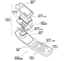
- H04M1/026—Details of the structure or mounting of specific components
- H04M1/0266—Details of the structure or mounting of specific components for a display module assembly
-
- H—ELECTRICITY
- H04—ELECTRIC COMMUNICATION TECHNIQUE
- H04M—TELEPHONIC COMMUNICATION
- H04M2250/00—Details of telephonic subscriber devices
- H04M2250/16—Details of telephonic subscriber devices including more than one display unit
-
- H—ELECTRICITY
- H04—ELECTRIC COMMUNICATION TECHNIQUE
- H04W—WIRELESS COMMUNICATION NETWORKS
- H04W52/00—Power management, e.g. TPC [Transmission Power Control], power saving or power classes
- H04W52/02—Power saving arrangements
- H04W52/0209—Power saving arrangements in terminal devices
- H04W52/0251—Power saving arrangements in terminal devices using monitoring of local events, e.g. events related to user activity
-
- Y—GENERAL TAGGING OF NEW TECHNOLOGICAL DEVELOPMENTS; GENERAL TAGGING OF CROSS-SECTIONAL TECHNOLOGIES SPANNING OVER SEVERAL SECTIONS OF THE IPC; TECHNICAL SUBJECTS COVERED BY FORMER USPC CROSS-REFERENCE ART COLLECTIONS [XRACs] AND DIGESTS
- Y02—TECHNOLOGIES OR APPLICATIONS FOR MITIGATION OR ADAPTATION AGAINST CLIMATE CHANGE
- Y02D—CLIMATE CHANGE MITIGATION TECHNOLOGIES IN INFORMATION AND COMMUNICATION TECHNOLOGIES [ICT], I.E. INFORMATION AND COMMUNICATION TECHNOLOGIES AIMING AT THE REDUCTION OF THEIR OWN ENERGY USE
- Y02D30/00—Reducing energy consumption in communication networks
- Y02D30/70—Reducing energy consumption in communication networks in wireless communication networks
Description
本発明は表示装置およびその駆動方法、特にホールド型を用いた表示装置の動画像の画質を向上する方法に関する。 The present invention relates to a display device and a driving method thereof, and more particularly to a method for improving the image quality of a moving image of a display device using a hold type.
近年、薄型の表示装置に対する関心が高まっている。CRTディスプレイに代わり、液晶ディスプレイ、プラズマディスプレイ、プロジェクションディスプレイなどが開発され、普及してきた。また、フィールドエミッションディスプレイ、無機エレクトロルミネセンスディスプレイ、有機エレクトロルミネセンスディスプレイ、電子ペーパーなどが、次世代の表示装置として開発が進められている。 In recent years, interest in thin display devices has increased. Instead of CRT displays, liquid crystal displays, plasma displays, projection displays and the like have been developed and spread. In addition, field emission displays, inorganic electroluminescent displays, organic electroluminescent displays, electronic paper, and the like are being developed as next-generation display devices.
上述したような表示装置に備えられた表示部には、画像を構成する最小単位である画素が並置される。そして、それぞれの画素は、画像データによって生成された信号を与えられることで、所望の輝度で発光する。その結果、表示部に画像が形成される。 In the display unit provided in the display device as described above, pixels that are the minimum unit constituting an image are juxtaposed. Each pixel emits light with a desired luminance by receiving a signal generated by image data. As a result, an image is formed on the display unit.
さらに、画素に与えられる信号は、一定の周期で更新(リフレッシュ)される。この、更新される周波数をフレームレートと呼ぶ。また、一度信号が更新されてから、次に更新されるまでの時間のことを、1フレーム期間と呼ぶ。表示部に動画を表示させるときは、信号が更新されるときに、前に与えられた信号とは異なる信号を画素に与えることで実現する。一方、表示部に静止画を表示させるときは、信号が更新されるときに、前に与えられた信号と同じ信号を画素に与える。 Furthermore, the signal given to the pixel is updated (refreshed) at a constant cycle. This updated frequency is called a frame rate. In addition, the time from when a signal is updated once until it is updated next is called one frame period. When a moving image is displayed on the display unit, when a signal is updated, a signal different from the signal given previously is given to the pixel. On the other hand, when a still image is displayed on the display unit, when the signal is updated, the same signal as the signal given before is given to the pixel.
また、表示装置の駆動方法は、画素の輝度が、1フレーム期間内に、どのような時間的分布を持っているかという観点で分類できる。アクティブマトリクス型の表示装置で用いられるホールド型では、画素は1フレーム期間内で継続して発光する。一方、CRTに代表されるインパルス型では、画素は1フレーム期間内に一度強く発光した後、直ちに減衰して発光しなくなる。インパルス型では、1フレーム期間の大半は非発光状態である。 In addition, the driving method of the display device can be classified from the viewpoint of what temporal distribution the pixel luminance has within one frame period. In a hold type used in an active matrix display device, a pixel continuously emits light within one frame period. On the other hand, in an impulse type typified by CRT, a pixel emits strong light once within one frame period, and then immediately attenuates and stops emitting light. In the impulse type, most of one frame period is a non-light emitting state.
ホールド型の表示装置は、動画を表示したとき、画像の一部分が動いている場合では動いているものが尾を引いたように見えたり、画像全体で動いている場合では全体がぼやけて見えたりする問題(動画ボケ:Motion Blur)を持つことが明らかになってきている。これは、ホールド型の表示装置の特性であり、インパルス型の表示装置では、動画ボケの問題は起こらない。 When a moving image is displayed, a hold-type display device may appear to have a trailing edge when it is moving part of the image, or it may appear blurry when it is moving as a whole image. It has become clear that it has a problem (moving motion blur). This is a characteristic of the hold type display device, and the moving image blur does not occur in the impulse type display device.
ホールド型の表示装置における動画ボケの問題を解決する方法としては、主に、次の2つの方法が提案されている(特許文献1)。1つ目は、1フレーム期間内において、本来の画像を表示する期間と、黒画像を表示する期間とを設けることである。こうすることで、表示をインパルス型に近づけることができるので、動画の画質を向上することができる(特許文献2、3)。
2つ目は、1フレーム期間の長さを短く(フレームレートを大きく)し、同時に、増えたフレームに関しては、時間的に補間された画像を生成し、表示を行なうことである。こうすることで、動画の画質を向上することができる(特許文献4)。さらに、1つ目の方法の改良技術として、黒画像の代わりに、元の画像より暗い画像を表示することでも動画の画質を向上することができることが公開されている(特許文献5、6、非特許文献1、2、3)。さらに、条件に応じて駆動方法を変える方法も公開されている(特許文献7、8)。
As a method of solving the problem of moving image blur in the hold type display device, the following two methods are mainly proposed (Patent Document 1). The first is to provide a period for displaying an original image and a period for displaying a black image within one frame period. By doing so, the display can be made closer to the impulse type, so that the image quality of the moving image can be improved (
The second is to shorten the length of one frame period (increase the frame rate), and at the same time, generate and display a temporally interpolated image for the increased number of frames. By doing so, the image quality of the moving image can be improved (Patent Document 4). Furthermore, as an improvement technique of the first method, it has been disclosed that the image quality of a moving image can be improved by displaying an image darker than the original image instead of the black image (
このように、ホールド型の表示装置における動画ボケの問題を解決する方法としては、様々なものが検討されているが、その効果が不十分である場合がある。また、その方法によって他の障害が増大してしまう場合もある。たとえば、黒画像を表示してインパルス型に近づける方法では、ちらつき(フリッカ)が増大する。さらに、黒画像の表示することによって、黒画像を挿入しない場合と比較すると画像の輝度が小さくなってしまう。その場合、黒画像を挿入しない場合と同等の輝度を得るためには、瞬間的に輝度を大きくする必要がある。その結果、表示装置にかかる負荷が増加することで信頼性を損なうことや消費電力が増大することが問題となる。 As described above, various methods for solving the problem of moving image blur in the hold-type display device have been studied, but the effect may be insufficient. In addition, other obstacles may increase depending on the method. For example, in the method of displaying a black image and bringing it closer to the impulse type, flickering increases. Furthermore, displaying a black image reduces the brightness of the image as compared to when no black image is inserted. In that case, it is necessary to increase the luminance instantaneously in order to obtain a luminance equivalent to that when no black image is inserted. As a result, increasing the load on the display device causes problems such as loss of reliability and increased power consumption.
フレームレートを大きくする方法では、データ処理が複雑になるため、高速に処理できる駆動回路が必要となり、製造コストの増加や、データ処理に伴う発熱や消費電力の増大が問題となる。さらに、画像データを補間して新しい画像を生成する方法では、質の高い補間画像を得ることは困難であり、補間したデータを挿入して表示することで、かえって動画の画質が低下してしまうこともある。 In the method of increasing the frame rate, data processing becomes complicated, so a drive circuit capable of high-speed processing is required, and there is a problem of increase in manufacturing cost, heat generation and power consumption accompanying data processing. Furthermore, it is difficult to obtain a high-quality interpolated image by a method of generating a new image by interpolating image data, and inserting and displaying the interpolated data lowers the quality of the moving image. Sometimes.
さらに、液晶を用いた表示装置に、前述の動画ボケの問題を解決する方法を適用する場合、液晶の透過率が変化する速度が遅く、信号の変化に対して十分に追従できないという問題がある。さらに、見る角度によって画素の発光の度合いが変わってしまう問題もある。 Furthermore, when the method for solving the above-mentioned moving image blur problem is applied to a display device using liquid crystal, there is a problem that the rate of change of the transmittance of the liquid crystal is slow and cannot sufficiently follow the change of the signal. . Furthermore, there is a problem that the degree of light emission of the pixel changes depending on the viewing angle.
本発明は、このような問題を鑑みてなされたものであり、動画ボケの問題がないホールド型の表示装置およびその駆動方法を提供することを課題とする。さらに、消費電力が低減された表示装置およびその駆動方法を提供すること、静止画および動画の画質がそれぞれ向上された表示装置およびその駆動方法を提供すること、視野角が向上された表示装置およびその駆動方法を提供すること、並びに液晶の応答速度が向上された表示装置およびその駆動方法を提供することを課題とする。 The present invention has been made in view of such problems, and an object of the present invention is to provide a hold-type display device that does not have a problem of moving image blur and a driving method thereof. Furthermore, providing a display device with reduced power consumption and a driving method thereof, providing a display device with improved image quality of still images and moving images and a driving method thereof, a display device with improved viewing angle, and It is an object of the present invention to provide a driving method thereof, and to provide a display device with improved response speed of liquid crystal and a driving method thereof.
本発明の一は、表示画面を有する液晶表示装置の駆動方法であって、前記表示画面において、1フレーム期間に複数の画像が表示され、前記複数の画像の少なくとも一は、物体が表示される画像であり、前記液晶表示装置が有する液晶素子は、前記物体が表示される画像を表示するための透過率を与える本来の電圧よりも大きな過大電圧で駆動され、前記物体が表示される画像の表示される期間が短くなるほど、前記過大電圧が大きくすることを特徴とする液晶表示装置の駆動方法である。 One aspect of the present invention is a method for driving a liquid crystal display device having a display screen, in which a plurality of images are displayed in one frame period on the display screen, and an object is displayed in at least one of the plurality of images. The liquid crystal element included in the liquid crystal display device is an image that is driven with an excessive voltage that is higher than an original voltage that provides a transmittance for displaying an image on which the object is displayed. The liquid crystal display device driving method is characterized in that the overvoltage is increased as the display period becomes shorter.
上記に加え、前記物体が表示される画像が表示される期間の長さは、前記液晶素子の透過率によって制御しても良い。また、上記液晶表示装置は、バックライトを有し、前記物体が表示される画像が表示される期間の長さは、前記バックライトの輝度によって制御しても良い。また、前記物体が表示される画像が表示される期間の長さは、前記液晶素子の透過率および前記バックライトの輝度によって制御しても良い。 In addition to the above, the length of the period during which the image on which the object is displayed is displayed may be controlled by the transmittance of the liquid crystal element. The liquid crystal display device may include a backlight, and the length of a period during which an image on which the object is displayed is displayed may be controlled by the luminance of the backlight. Further, the length of the period during which the image displaying the object is displayed may be controlled by the transmittance of the liquid crystal element and the luminance of the backlight.
また、複数のエリアに分割されたバックライトを有し、前記物体が表示される画像が表示される期間の長さは、前記複数のエリアに分割されたのバックライトの輝度によって制御しても良いし、複数のバックライトを有し、前記物体が表示される画像が表示される期間の長さは、前記液晶素子の透過率および前記複数のエリアに分割されたバックライトの輝度によって制御しても良い。 In addition, the backlight may be divided into a plurality of areas, and the length of the period during which the image on which the object is displayed is displayed may be controlled by the luminance of the backlight divided into the plurality of areas. In addition, the length of the period during which an image on which the object is displayed having a plurality of backlights is displayed is controlled by the transmittance of the liquid crystal element and the luminance of the backlight divided into the plurality of areas. May be.
また、本発明の一は、表示画面および制御回路を有する液晶表示装置であって、前記表示画面において、1フレーム期間に複数の画像が表示され、前記複数の画像の少なくとも一は、物体が表示される画像であり、前記液晶表示装置が有する液晶素子は、前記物体が表示される画像を表示するための透過率を与える本来の電圧よりも大きな過大電圧で駆動され、前記制御回路は、前記物体が表示される画像の表示される期間が短くなるほど、前記過大電圧が大きくする機能を有することを特徴とする液晶表示装置である。 Another aspect of the present invention is a liquid crystal display device having a display screen and a control circuit, wherein a plurality of images are displayed in one frame period on the display screen, and at least one of the plurality of images is displayed by an object. The liquid crystal element included in the liquid crystal display device is driven with an excessive voltage larger than an original voltage that provides transmittance for displaying an image on which the object is displayed, and the control circuit The liquid crystal display device has a function of increasing the excessive voltage as a display period of an image on which an object is displayed becomes shorter.
上記液晶表示装置の制御回路は、さらに、前記物体が表示される画像が表示される期間の長さを、前記液晶素子の透過率によって制御する機能を有していても良い。また、上記液晶表示装置は、バックライトを有し、前記制御回路は、さらに、前記物体が表示される画像が表示される期間の長さを、前記バックライトの輝度によって制御する機能を有していても良い。また、複数のエリアに分割されたバックライトを有し、前記制御回路は、さらに、前記物体が表示される画像が表示される期間の長さを、前記複数のエリアに分割されたバックライトの輝度によって制御する機能を有していても良い。 The control circuit of the liquid crystal display device may further have a function of controlling a length of a period during which an image on which the object is displayed is displayed by a transmittance of the liquid crystal element. In addition, the liquid crystal display device includes a backlight, and the control circuit further has a function of controlling the length of a period during which an image on which the object is displayed is displayed by the luminance of the backlight. May be. A backlight divided into a plurality of areas, and the control circuit further determines a length of a period during which an image on which the object is displayed is displayed, of the backlight divided into the plurality of areas. You may have the function controlled by a brightness | luminance.
また、上記液晶表示装置は、バックライトを有し、前記制御回路は、さらに、前記物体が表示される画像が表示される期間の長さを、前記液晶素子の透過率および前記バックライトの輝度によって制御しても良い。 The liquid crystal display device includes a backlight, and the control circuit further determines a length of a period during which an image on which the object is displayed is displayed, a transmittance of the liquid crystal element, and a luminance of the backlight. You may control by.
また、上記液晶表示装置は、複数のエリアに分割されたバックライトを有し、前記制御回路は、さらに、前記物体が表示される画像が表示される期間の長さを、前記液晶素子の透過率および前記複数のエリアに分割されたバックライトの輝度によって制御しても良い。 In addition, the liquid crystal display device includes a backlight divided into a plurality of areas, and the control circuit further determines a length of a period during which an image on which the object is displayed is displayed, through the transmission of the liquid crystal element. You may control according to a rate and the brightness | luminance of the backlight divided | segmented into the said several area.
なお、1フレーム期間は複数のサブフレーム期間に分割されており、それぞれのサブフレーム期間は画像表示期間、ブランク期間等のいずれか一に属する。例え、サブフレーム期間がブランク期間であっても一画像を表示していると認識することも可能であるため、上記においては一サブフレーム期間につき一画像が表示されているものとする。 One frame period is divided into a plurality of subframe periods, and each subframe period belongs to any one of an image display period, a blank period, and the like. For example, since it is possible to recognize that one image is displayed even if the subframe period is a blank period, in the above description, it is assumed that one image is displayed per one subframe period.
なお、本明細書において、輝度が0であると表現するときは、全く光っていない状態に加えて、実質的に黒を表示している場合も含む。つまり、微量に光を発していても、表示できる階調のうち一番暗い階調を表示している場合は、輝度が0であると表現することがある。 Note that in this specification, the expression that the luminance is 0 includes a case where substantially black is displayed in addition to a state where no light is emitted. In other words, even when a very small amount of light is emitted, when the darkest gradation among the displayable gradations is displayed, the luminance may be expressed as zero.
なお、本書類(明細書、特許請求の範囲又は図面など)に示すスイッチは、様々な形態のものを用いることができる。例としては、電気的スイッチや機械的なスイッチなどがある。つまり、電流の流れを制御できるものであればよく、特定のものに限定されない。例えば、スイッチとして、トランジスタ(例えば、バイポーラトランジスタ、MOSトランジスタなど)、ダイオード(例えば、PNダイオード、PINダイオード、ショットキーダイオード、MIM(Metal Insulator Metal)ダイオード、MIS(Metal Insulator Semiconductor)ダイオード、ダイオード接続のトランジスタなど)、サイリスタなどを用いることが出来る。または、これらを組み合わせた論理回路をスイッチとして用いることが出来る。 Note that a variety of switches can be used as a switch described in this document (specification, claims, drawings, or the like). Examples include electrical switches and mechanical switches. That is, it is only necessary to be able to control the current flow, and is not limited to a specific one. For example, as a switch, a transistor (for example, bipolar transistor, MOS transistor, etc.), a diode (for example, PN diode, PIN diode, Schottky diode, MIM (Metal Insulator Metal) diode, MIS (Metal Insulator Semiconductor) diode, diode-connected Transistor), a thyristor, or the like can be used. Alternatively, a logic circuit combining these can be used as a switch.
スイッチとしてトランジスタを用いる場合、そのトランジスタは、単なるスイッチとして動作するため、トランジスタの極性(導電型)は特に限定されない。ただし、オフ電流を抑えたい場合、オフ電流が少ない方の極性のトランジスタを用いることが望ましい。オフ電流が少ないトランジスタとしては、LDD領域を有するトランジスタやマルチゲート構造を有するトランジスタ等がある。または、スイッチとして動作させるトランジスタのソース端子の電位が、低電位側電源(Vss、GND、0Vなど)の電位に近い状態で動作する場合はNチャネル型トランジスタを用いることが望ましい。反対に、ソース端子の電位が、高電位側電源(Vddなど)の電位に近い状態で動作する場合はPチャネル型トランジスタを用いることが望ましい。なぜなら、Nチャネル型トランジスタではソース端子が低電位側電源の電位に近い状態で動作するとき、Pチャネル型トランジスタではソース端子が高電位側電源の電位に近い状態で動作するとき、ゲートソース間電圧の絶対値を大きくできるため、スイッチとして、動作しやすいからである。また、ソースフォロワ動作をしてしまうことが少ないため、出力電圧の大きさが小さくなってしまうことが少ないからである。 In the case where a transistor is used as a switch, the transistor operates as a mere switch, and thus the polarity (conductivity type) of the transistor is not particularly limited. However, when it is desired to suppress off-state current, it is desirable to use a transistor having a polarity with smaller off-state current. As a transistor with low off-state current, a transistor having an LDD region, a transistor having a multi-gate structure, and the like can be given. Alternatively, an N-channel transistor is preferably used in the case where the transistor operates as a switch when the potential of the source terminal of the transistor is close to the potential of the low potential power supply (Vss, GND, 0 V, or the like). On the other hand, it is desirable to use a P-channel transistor when operating in a state where the potential of the source terminal is close to the potential of the high potential side power supply (Vdd or the like). This is because when the N-channel transistor operates with the source terminal close to the potential of the low-potential side power supply, and the P-channel transistor operates with the source terminal close to the potential of the high-potential side power supply, This is because it is easy to operate as a switch because the absolute value of can be increased. Moreover, since the source follower operation is rarely performed, the output voltage is rarely reduced.
なお、Nチャネル型トランジスタとPチャネル型トランジスタの両方を用いて、CMOS型のスイッチをスイッチとして用いてもよい。CMOS型のスイッチにすると、Pチャネル型トランジスタまたはNチャネル型トランジスタのどちらか一方のトランジスタが導通すれば電流が流れるため、スイッチとして機能しやすくなる。例えば、スイッチへの入力信号の電圧が高い場合でも、低い場合でも、適切に電圧を出力させることが出来る。さらに、スイッチをオン・オフさせるための信号の電圧振幅値を小さくすることが出来るので、消費電力を小さくすることも出来る。 Note that a CMOS switch may be used as a switch by using both an N-channel transistor and a P-channel transistor. When a CMOS switch is used, a current flows when one of the P-channel transistor and the N-channel transistor is turned on, so that the switch can easily function as a switch. For example, the voltage can be appropriately output regardless of whether the voltage of the input signal to the switch is high or low. Furthermore, since the voltage amplitude value of the signal for turning on / off the switch can be reduced, the power consumption can be reduced.
なお、スイッチとしてトランジスタを用いる場合、スイッチは、入力端子(ソース端子またはドレイン端子の一方)と、出力端子(ソース端子またはドレイン端子の他方)と、導通を制御する端子(ゲート端子)とを有している。一方、スイッチとしてダイオードを用いる場合、スイッチは、導通を制御する端子を有していない場合がある。そのため、トランジスタよりもダイオードをスイッチとして用いた方が、端子を制御するための配線を少なくすることが出来る。 Note that when a transistor is used as a switch, the switch has an input terminal (one of a source terminal or a drain terminal), an output terminal (the other of the source terminal or the drain terminal), and a terminal for controlling conduction (a gate terminal). doing. On the other hand, when a diode is used as the switch, the switch may not have a terminal for controlling conduction. Therefore, the use of a diode as a switch rather than a transistor can reduce the wiring for controlling the terminal.
なお、本書類(明細書、特許請求の範囲又は図面など)において、AとBとが接続されている、と明示的に記載する場合は、AとBとが電気的に接続されている場合と、AとBとが機能的に接続されている場合と、AとBとが直接接続されている場合とを含むものとする。ここで、A、Bは、対象物(例えば、装置、素子、回路、配線、電極、端子、導電膜、層、など)であるとする。したがって、本書類(明細書、特許請求の範囲又は図面など)が開示する構成において、所定の接続関係、例えば、図または文章に示された接続関係に限定されず、図または文章に示された接続関係以外のものも含むものとする。 In addition, in this document (specifications, claims, drawings, etc.), when it is explicitly stated that A and B are connected, A and B are electrically connected And A and B are functionally connected and A and B are directly connected. Here, A and B are objects (for example, devices, elements, circuits, wirings, electrodes, terminals, conductive films, layers, etc.). Therefore, in the configuration disclosed in this document (specifications, claims, drawings, etc.), it is not limited to a predetermined connection relationship, for example, the connection relationship shown in the figure or text, but is shown in the figure or text. Including those other than connection relations.
例えば、AとBとが電気的に接続されている場合として、AとBとの電気的な接続を可能とする素子(例えば、スイッチ、トランジスタ、容量素子、インダクタ、抵抗素子、ダイオードなど)が、AとBとの間に1個以上配置されていてもよい。あるいは、AとBとが機能的に接続されている場合として、AとBとの機能的な接続を可能とする回路(例えば、論理回路(インバータ、NAND回路、NOR回路など)、信号変換回路(DA変換回路、AD変換回路、ガンマ補正回路など)、電位レベル変換回路(電源回路(昇圧回路、降圧回路など)、信号の電位レベルを変えるレベルシフタ回路など)、電圧源、電流源、切り替え回路、増幅回路(信号振幅または電流量などを大きく出来る回路、オペアンプ、差動増幅回路、ソースフォロワ回路、バッファ回路など)、信号生成回路、記憶回路、制御回路など)が、AとBとの間に1個以上配置されていてもよい。あるいは、AとBとが直接接続されている場合として、AとBとの間に他の素子や他の回路を挟まずに、AとBとが直接接続されていてもよい。 For example, when A and B are electrically connected, an element (for example, a switch, a transistor, a capacitor, an inductor, a resistance element, a diode, or the like) that enables electrical connection between A and B is provided. 1 or more may be arranged between A and B. Alternatively, when A and B are functionally connected, a circuit (for example, a logic circuit (an inverter, a NAND circuit, a NOR circuit, etc.), a signal conversion circuit that enables functional connection between A and B (DA conversion circuit, AD conversion circuit, gamma correction circuit, etc.), potential level conversion circuit (power supply circuit (boost circuit, step-down circuit, etc.), level shifter circuit that changes signal potential level), voltage source, current source, switching circuit , Amplifier circuits (circuits that can increase signal amplitude or current amount, operational amplifiers, differential amplifier circuits, source follower circuits, buffer circuits, etc.), signal generation circuits, memory circuits, control circuits, etc.) between A and B One or more of them may be arranged. Alternatively, when A and B are directly connected, A and B may be directly connected without sandwiching other elements or other circuits between A and B.
なお、AとBとが直接接続されている、と明示的に記載する場合は、AとBとが直接接続されている場合(つまり、AとBとの間に他の素子や他の回路を間に介さずに接続されている場合)と、AとBとが電気的に接続されている場合(つまり、AとBとの間に別の素子や別の回路を挟んで接続されている場合)とを含むものとする。 Note that in the case where it is explicitly described that A and B are directly connected, when A and B are directly connected (that is, another element or other circuit between A and B). ) And A and B are electrically connected (that is, A and B are connected with another element or another circuit sandwiched between them). ).
なお、AとBとが電気的に接続されている、と明示的に記載する場合は、AとBとが電気的に接続されている場合(つまり、AとBとの間に別の素子や別の回路を挟んで接続されている場合)と、AとBとが機能的に接続されている場合(つまり、AとBとの間に別の回路を挟んで機能的に接続されている場合)と、AとBとが直接接続されている場合(つまり、AとBとの間に別の素子や別の回路を挟まずに接続されている場合)とを含むものとする。つまり、電気的に接続されている、と明示的に記載する場合は、単に、接続されている、とのみ明示的に記載されている場合と同じであるとする。 Note that in the case where it is explicitly described that A and B are electrically connected, another element is connected between A and B (that is, between A and B). Or when A and B are functionally connected (that is, they are functionally connected with another circuit between A and B). And a case where A and B are directly connected (that is, a case where another element or another circuit is not connected between A and B). That is, when it is explicitly described that it is electrically connected, it is the same as when it is explicitly only described that it is connected.
なお、表示素子、表示素子を有する装置である表示装置、発光素子、発光素子を有する装置である発光装置は、様々な形態を用いたり、様々な素子を有したりすることが出来る。例えば、表示素子、表示装置、発光素子または発光装置としては、EL素子(有機物及び無機物を含むEL素子、有機EL素子、無機EL素子)、電子放出素子、液晶素子、電子インク、電気泳動素子、グレーティングライトバルブ(GLV)、プラズマディスプレイ(PDP)、デジタルマイクロミラーデバイス(DMD)、圧電セラミックディスプレイ、カーボンナノチューブ、など、電気磁気的作用により、コントラスト、輝度、反射率、透過率などが変化する表示媒体を用いることができる。なお、EL素子を用いた表示装置としてはELディスプレイ、電子放出素子を用いた表示装置としてはフィールドエミッションディスプレイ(FED)やSED方式平面型ディスプレイ(SED:Surface−conduction Electron−emitter Disply)など、液晶素子を用いた表示装置としては液晶ディスプレイ(透過型液晶ディスプレイ、半透過型液晶ディスプレイ、反射型液晶ディスプレイ、直視型液晶ディスプレイ、投射型液晶ディスプレイ)、電子インクや電気泳動素子を用いた表示装置としては電子ペーパーがある。 Note that a display element, a display device that is a device including a display element, a light-emitting element, and a light-emitting device that is a device including a light-emitting element can have various modes or have various elements. For example, as a display element, a display device, a light-emitting element, or a light-emitting device, an EL element (an EL element including an organic substance and an inorganic substance, an organic EL element, an inorganic EL element), an electron-emitting element, a liquid crystal element, electronic ink, an electrophoretic element, Grating light valve (GLV), plasma display (PDP), digital micromirror device (DMD), piezoelectric ceramic display, carbon nanotube, and other displays that change contrast, brightness, reflectivity, transmittance, etc. due to electromagnetic action Media can be used. Note that a display device using an EL element is an EL display, and a display device using an electron-emitting device is a liquid crystal display such as a field emission display (FED) or a SED type flat display (SED: Surface-conduction Electron-Emitter Display). Liquid crystal displays (transmission type liquid crystal display, transflective type liquid crystal display, reflection type liquid crystal display, direct view type liquid crystal display, projection type liquid crystal display), display devices using electronic ink and electrophoretic elements There is electronic paper.
なお、微結晶シリコンを製造するときに、触媒(ニッケルなど)を用いることにより、結晶性をさらに向上させ、電気特性のよいトランジスタを製造することが可能となる。このとき、レーザーを用いず、熱処理を加えるだけで、結晶性を向上させることができる。その結果、ゲートドライバ回路(走査線駆動回路)やソースドライバ回路の一部(アナログスイッチなど)を基板上に一体形成することが出来る。さらに、結晶化のためにレーザーを用いない場合は、シリコンの結晶性のムラを抑えることができる。そのため、綺麗な画像を表示することが出来る。 Note that when a microcrystalline silicon is manufactured, by using a catalyst (such as nickel), crystallinity can be further improved and a transistor with favorable electrical characteristics can be manufactured. At this time, crystallinity can be improved only by applying heat treatment without using a laser. As a result, a part of the gate driver circuit (scanning line driver circuit) and the source driver circuit (analog switch or the like) can be integrally formed on the substrate. Further, when a laser is not used for crystallization, unevenness in crystallinity of silicon can be suppressed. Therefore, a beautiful image can be displayed.
ただし、触媒(ニッケルなど)を用いずに、多結晶シリコンや微結晶シリコンを製造することは可能である。 However, it is possible to produce polycrystalline silicon or microcrystalline silicon without using a catalyst (such as nickel).
または、半導体基板やSOI基板などを用いてトランジスタを形成することが出来る。これらにより、特性やサイズや形状などのバラツキが少なく、電流供給能力が高く、サイズの小さいトランジスタを製造することができる。これらのトランジスタを用いると、回路の低消費電力化、又は回路の高集積化を図ることができる。 Alternatively, a transistor can be formed using a semiconductor substrate, an SOI substrate, or the like. Accordingly, a transistor with small variations in characteristics, size, shape, and the like, high current supply capability, and small size can be manufactured. When these transistors are used, low power consumption of the circuit or high integration of the circuit can be achieved.
または、ZnO、a−InGaZnO、SiGe、GaAs、IZO、ITO、SnOなどの化合物半導体または酸化物半導体を有するトランジスタや、さらに、これらの化合物半導体または酸化物半導体を薄膜化した薄膜トランジスタなどを用いることが出来る。これらにより、製造温度を低くでき、例えば、室温でトランジスタを製造することが可能となる。その結果、耐熱性の低い基板、例えばプラスチック基板やフィルム基板に直接トランジスタを形成することが出来る。なお、これらの化合物半導体または酸化物半導体を、トランジスタのチャネル部分に用いるだけでなく、それ以外の用途で用いることも出来る。例えば、これらの化合物半導体または酸化物半導体を抵抗素子、画素電極、透明電極として用いることができる。さらに、それらをトランジスタと同時に成膜又は形成できるため、コストを低減できる。 Alternatively, a transistor having a compound semiconductor or an oxide semiconductor such as ZnO, a-InGaZnO, SiGe, GaAs, IZO, ITO, or SnO, or a thin film transistor in which these compound semiconductor or oxide semiconductor is thinned can be used. I can do it. Accordingly, the manufacturing temperature can be lowered, and for example, the transistor can be manufactured at room temperature. As a result, the transistor can be formed directly on a substrate having low heat resistance, such as a plastic substrate or a film substrate. Note that these compound semiconductors or oxide semiconductors can be used not only for a channel portion of a transistor but also for other purposes. For example, these compound semiconductors or oxide semiconductors can be used as resistance elements, pixel electrodes, and transparent electrodes. Furthermore, since these can be formed or formed simultaneously with the transistor, cost can be reduced.
または、インクジェットや印刷法を用いて形成したトランジスタなどを用いることが出来る。これらにより、室温で製造、低真空度で製造、又は大型基板上に製造することができる。また、マスク(レチクル)を用いなくても製造することが可能となるため、トランジスタのレイアウトを容易に変更することが出来る。さらに、レジストを用いる必要がないので、材料費が安くなり、工程数を削減できる。さらに、必要な部分にのみ膜を付けるため、全面に成膜した後でエッチングする、という製法よりも、材料が無駄にならず、低コストにできる。 Alternatively, a transistor formed using an inkjet method or a printing method can be used. By these, it can manufacture at room temperature, manufacture at a low vacuum degree, or can manufacture on a large sized board | substrate. Further, since the transistor can be manufactured without using a mask (reticle), the layout of the transistor can be easily changed. Furthermore, since it is not necessary to use a resist, the material cost is reduced and the number of processes can be reduced. Further, since a film is formed only on a necessary portion, the material is not wasted and cost can be reduced as compared with a manufacturing method in which etching is performed after film formation on the entire surface.
または、有機半導体やカーボンナノチューブを有するトランジスタ等を用いることができる。これらにより、曲げることが可能な基板上にトランジスタを形成することが出来る。そのため、衝撃に強くできる。 Alternatively, a transistor including an organic semiconductor or a carbon nanotube can be used. Thus, a transistor can be formed over a substrate that can be bent. Therefore, it can be strong against impact.
さらに、様々な構造のトランジスタを用いることができる。例えば、MOS型トランジスタ、接合型トランジスタ、バイポーラトランジスタなどを本書類(明細書、特許請求の範囲又は図面など)に記載されたトランジスタとして用いることが出来る。MOS型トランジスタを用いることにより、トランジスタのサイズを小さくすることが出来る。よって、多数のトランジスタを搭載することができる。バイポーラトランジスタを用いることにより、大きな電流を流すことが出来る。よって、高速に回路を動作させることができる。 In addition, transistors with various structures can be used. For example, a MOS transistor, a junction transistor, a bipolar transistor, or the like can be used as the transistor described in this document (the specification, the claims, the drawings, or the like). By using a MOS transistor, the size of the transistor can be reduced. Therefore, a large number of transistors can be mounted. By using a bipolar transistor, a large current can flow. Therefore, the circuit can be operated at high speed.
なお、MOS型トランジスタ、バイポーラトランジスタなどを1つの基板に混在させて形成してもよい。これにより、低消費電力、小型化、高速動作などを実現することが出来る。 Note that a MOS transistor, a bipolar transistor, or the like may be formed over one substrate. Thereby, low power consumption, miniaturization, high-speed operation, etc. can be realized.
その他、様々なトランジスタを用いることができる。 In addition, various transistors can be used.
なお、トランジスタが形成されている基板の種類は、様々なものを用いることができ、特定のものに限定されることはない。トランジスタが形成される基板としては、例えば、単結晶基板、SOI基板、ガラス基板、石英基板、プラスチック基板、紙基板、セロファン基板、石材基板、木材基板、布基板(天然繊維(絹、綿、麻)、合成繊維(ナイロン、ポリウレタン、ポリエステル)若しくは再生繊維(アセテート、キュプラ、レーヨン、再生ポリエステル)などを含む)、皮革基板、ゴム基板、ステンレス・スチル基板、ステンレス・スチル・ホイルを有する基板などを用いることが出来る。あるいは、人などの動物の皮膚(皮表、真皮)又は皮下組織を基板として用いてもよい。または、ある基板でトランジスタを形成し、その後、別の基板にトランジスタを転置し、別の基板上にトランジスタを配置してもよい。トランジスタが転置される基板としては、単結晶基板、SOI基板、ガラス基板、石英基板、プラスチック基板、紙基板、セロファン基板、石材基板、、木材基板、布基板(天然繊維(絹、綿、麻)、合成繊維(ナイロン、ポリウレタン、ポリエステル)若しくは再生繊維(アセテート、キュプラ、レーヨン、再生ポリエステル)などを含む)、皮革基板、ゴム基板、ステンレス・スチル基板、ステンレス・スチル・ホイルを有する基板などを用いることができる。あるいは、人などの動物の皮膚(皮表、真皮)又は皮下組織を基板として用いてもよい。または、ある基板でトランジスタを形成し、その基板を研磨して薄くしてもよい。研磨される基板としては、単結晶基板、SOI基板、ガラス基板、石英基板、プラスチック基板、紙基板、セロファン基板、石材基板、、木材基板、布基板(天然繊維(絹、綿、麻)、合成繊維(ナイロン、ポリウレタン、ポリエステル)若しくは再生繊維(アセテート、キュプラ、レーヨン、再生ポリエステル)などを含む)、皮革基板、ゴム基板、ステンレス・スチル基板、ステンレス・スチル・ホイルを有する基板などを用いることができる。あるいは、人などの動物の皮膚(皮表、真皮)又は皮下組織を基板として用いてもよい。これらの基板を用いることにより、特性のよいトランジスタの形成、消費電力の小さいトランジスタの形成、壊れにくい装置の製造、耐熱性の付与、軽量化、又は薄型化を図ることができる。 Note that various types of substrates on which transistors are formed can be used and are not limited to specific types. As a substrate on which a transistor is formed, for example, a single crystal substrate, an SOI substrate, a glass substrate, a quartz substrate, a plastic substrate, a paper substrate, a cellophane substrate, a stone substrate, a wood substrate, a cloth substrate (natural fiber (silk, cotton, hemp) ), Synthetic fibers (nylon, polyurethane, polyester) or recycled fibers (including acetate, cupra, rayon, recycled polyester), leather substrates, rubber substrates, stainless steel substrates, substrates with stainless steel foil, etc. Can be used. Alternatively, the skin (skin surface, dermis) or subcutaneous tissue of an animal such as a human may be used as the substrate. Alternatively, a transistor may be formed over a certain substrate, and then the transistor may be transferred to another substrate, and the transistor may be disposed over another substrate. The substrate to which the transistor is transferred is a single crystal substrate, SOI substrate, glass substrate, quartz substrate, plastic substrate, paper substrate, cellophane substrate, stone substrate, wood substrate, cloth substrate (natural fiber (silk, cotton, hemp) , Synthetic fibers (including nylon, polyurethane, polyester) or recycled fibers (including acetate, cupra, rayon, recycled polyester), leather substrates, rubber substrates, stainless steel substrates, substrates with stainless steel foil, etc. be able to. Alternatively, the skin (skin surface, dermis) or subcutaneous tissue of an animal such as a human may be used as the substrate. Alternatively, a transistor may be formed using a certain substrate, and the substrate may be polished and thinned. As substrates to be polished, single crystal substrate, SOI substrate, glass substrate, quartz substrate, plastic substrate, paper substrate, cellophane substrate, stone substrate, wood substrate, cloth substrate (natural fiber (silk, cotton, hemp), synthetic Use fibers (including nylon, polyurethane, polyester) or recycled fibers (including acetate, cupra, rayon, recycled polyester), leather substrates, rubber substrates, stainless steel substrates, substrates with stainless steel foil, etc. it can. Alternatively, the skin (skin surface, dermis) or subcutaneous tissue of an animal such as a human may be used as the substrate. By using these substrates, it is possible to form a transistor with good characteristics, a transistor with low power consumption, manufacture a device that is not easily broken, impart heat resistance, reduce weight, or reduce thickness.
なお、トランジスタの構成は、様々な形態をとることができる。特定の構成に限定されない。例えば、ゲート電極が2個以上のマルチゲート構造を用いてもよい。マルチゲート構造にすると、チャネル領域が直列に接続されるため、複数のトランジスタが直列に接続された構成となる。マルチゲート構造により、オフ電流の低減、トランジスタの耐圧向上による信頼性の向上を図ることができる。あるいは、マルチゲート構造により、飽和領域で動作する時に、ドレイン・ソース間電圧が変化しても、ドレイン・ソース間電流があまり変化せず、電圧・電流特性の傾きがフラットな特性にすることができる。電圧・電流特性の傾きがフラットである特性を利用すると、理想的な電流源回路や、非常に高い抵抗値をもつ能動負荷を実現することが出来る。その結果、特性のよい差動回路やカレントミラー回路を実現することが出来る。また、チャネルの上下にゲート電極が配置されている構造でもよい。チャネルの上下にゲート電極が配置されている構造にすることにより、チャネル領域が増えるため、電流値の増加、又は空乏層ができやすくなることによるS値の低減を図ることができる。を小さくしたりすることができる。チャネルの上下にゲート電極が配置されると、複数のトランジスタが並列に接続されたような構成となる。 Note that the structure of the transistor can take a variety of forms. It is not limited to a specific configuration. For example, a multi-gate structure having two or more gate electrodes may be used. When the multi-gate structure is employed, the channel regions are connected in series, so that a plurality of transistors are connected in series. With the multi-gate structure, the off-state current can be reduced and the reliability can be improved by improving the withstand voltage of the transistor. Or, when operating in the saturation region, the drain-source current does not change much even when the drain-source voltage changes, and the slope of the voltage / current characteristic is flat due to the multi-gate structure. it can. By using the characteristic that the slope of the voltage / current characteristic is flat, an ideal current source circuit and an active load having a very high resistance value can be realized. As a result, a differential circuit or a current mirror circuit with good characteristics can be realized. Alternatively, a structure in which gate electrodes are arranged above and below the channel may be employed. With the structure in which the gate electrodes are arranged above and below the channel, the channel region increases, so that the current value can be increased or the S value can be reduced because a depletion layer can be easily formed. Can be made smaller. When gate electrodes are provided above and below a channel, a structure in which a plurality of transistors are connected in parallel is obtained.
あるいは、チャネル領域の上にゲート電極が配置されている構造でもよいし、チャネル領域の下にゲート電極が配置されている構造でもよい。あるいは、正スタガ構造または逆スタガ構造でもよいし、チャネル領域が複数の領域に分かれていてもよいし、チャネル領域が並列に接続されていてもよいし、チャネル領域が直列に接続されていてもよい。また、チャネル領域(もしくはその一部)にソース電極やドレイン電極が重なっていてもよい。チャネル領域(もしくはその一部)にソース電極やドレイン電極が重なる構造にすることにより、チャネル領域の一部に電荷がたまって、動作が不安定になることを防ぐことができる。また、LDD領域を設けても良い。LDD領域を設けることにより、オフ電流の低減、又はトランジスタの耐圧向上による信頼性の向上を図ることができる。あるいは、LDD領域を設けることにより、飽和領域で動作する時に、ドレイン・ソース間電圧が変化しても、ドレイン・ソース間電流があまり変化せず、電圧・電流特性の傾きがフラットな特性にすることができる。 Alternatively, a structure in which a gate electrode is disposed over a channel region may be employed, or a structure in which a gate electrode is disposed under a channel region may be employed. Alternatively, a normal stagger structure or an inverted stagger structure may be used, the channel region may be divided into a plurality of regions, the channel regions may be connected in parallel, or the channel regions may be connected in series. Good. In addition, a source electrode or a drain electrode may overlap with the channel region (or a part thereof). With the structure in which the source electrode or the drain electrode overlaps with the channel region (or part thereof), it is possible to prevent electric charges from being accumulated in part of the channel region and unstable operation. Further, an LDD region may be provided. By providing the LDD region, the off-state current can be reduced or the reliability can be improved by improving the withstand voltage of the transistor. Alternatively, by providing an LDD region, when operating in the saturation region, even if the drain-source voltage changes, the drain-source current does not change so much and the slope of the voltage-current characteristic is flat. be able to.
なお、本書類(明細書、特許請求の範囲又は図面など)におけるトランジスタは、様々なタイプを用いることができ、様々な基板上に形成させることができる。したがって、所定の機能を実現させるために必要な回路の全てが、同一の基板に形成されていてもよい。例えば、所定の機能を実現させるために必要な回路の全てが、ガラス基板、プラスチック基板、単結晶基板、またはSOI基板上に形成されていてもよく、さまざまな基板上に形成されていてもよい。所定の機能を実現させるために必要な回路の全てが同じ基板上に形成されていることにより、部品点数の削減によるコストの低減、又は回路部品との接続点数の低減による信頼性の向上を図ることができる。あるいは、所定の機能を実現させるために必要な回路の一部が、ある基板に形成されており、所定の機能を実現させるために必要な回路の別の一部が、別の基板に形成されていてもよい。つまり、所定の機能を実現させるために必要な回路の全てが同じ基板上に形成されていなくてもよい。例えば、所定の機能を実現させるために必要な回路の一部は、ガラス基板上にトランジスタを用いて形成され、所定の機能を実現させるために必要な回路の別の一部は、単結晶基板上に形成され、単結晶基板上のトランジスタで構成されたICチップをCOG(Chip On Glass)でガラス基板に接続して、ガラス基板上にそのICチップを配置してもよい。あるいは、そのICチップをTAB(Tape Automated Bonding)やプリント基板を用いてガラス基板と接続してもよい。このように、回路の一部が同じ基板に形成されていることにより、部品点数の削減によるコストの低減、又は回路部品との接続点数の低減による信頼性の向上を図ることができる。また、駆動電圧が高い部分や駆動周波数が高い部分の回路は、消費電力が大きくなってしまうので、そのような部分の回路は同じ基板に形成せず、そのかわりに、例えば、単結晶基板上にその部分の回路を形成して、その回路で構成されたICチップを用いるようにすれば、消費電力の増加を防ぐことができる。 Note that various types of transistors can be used for the transistor in this document (the specification, the claims, the drawings, and the like) and can be formed over various substrates. Therefore, all of the circuits necessary for realizing a predetermined function may be formed on the same substrate. For example, all circuits necessary for realizing a predetermined function may be formed over a glass substrate, a plastic substrate, a single crystal substrate, or an SOI substrate, or may be formed over various substrates. . Since all the circuits necessary for realizing a predetermined function are formed on the same substrate, the cost can be reduced by reducing the number of components, or the reliability can be improved by reducing the number of connection points with circuit components. be able to. Alternatively, a part of the circuit necessary for realizing the predetermined function is formed on a certain substrate, and another part of the circuit necessary for realizing the predetermined function is formed on another substrate. It may be. That is, not all of the circuits necessary for realizing a predetermined function may be formed on the same substrate. For example, a part of a circuit necessary for realizing a predetermined function is formed using a transistor over a glass substrate, and another part of a circuit required for realizing a predetermined function is a single crystal substrate. The IC chip formed on the single crystal substrate and formed of a transistor may be connected to the glass substrate by COG (Chip On Glass), and the IC chip may be arranged on the glass substrate. Alternatively, the IC chip may be connected to the glass substrate using TAB (Tape Automated Bonding) or a printed board. As described above, since a part of the circuit is formed on the same substrate, the cost can be reduced by reducing the number of components, or the reliability can be improved by reducing the number of connection points with circuit components. In addition, since the power consumption of a circuit having a high driving voltage or a high driving frequency is large, such a circuit is not formed on the same substrate. Instead, for example, on a single crystal substrate. If the circuit of that portion is formed and an IC chip constituted by the circuit is used, an increase in power consumption can be prevented.
なお、本書類(明細書、特許請求の範囲又は図面など)においては、一画素とは、明るさを制御できる要素一つ分を示すものとする。よって、一例としては、一画素とは、一つの色要素を示すものとし、その色要素一つで明るさを表現する。従って、そのときは、R(赤)G(緑)B(青)の色要素からなるカラー表示装置の場合には、画像の最小単位は、Rの画素とGの画素とBの画素との三画素から構成されるものとする。なお、色要素は、三色に限定されず、三色以上を用いても良いし、RGB以外の色を用いても良い。例えば、白色を加えて、RGBW(Wは白)としてもよい。また、RGBに、例えば、イエロー、シアン、マゼンタ、エメラルドグリーン、朱色などを一色以上追加してもよい。また、例えば、RGBの中の少なくとも一色に類似した色を、RGBに追加してもよい。例えば、R、G、B1、B2としてもよい。B1とB2とは、どちらも青色であるが、少し周波数が異なっている。同様に、R1、R2、G、Bとしてもよい。このような色要素を用いることにより、より実物に近い表示を行うことができる。あるいは、このような色要素を用いることにより、消費電力を低減することが出来る。また、別の例としては、1つの色要素について、複数の領域を用いて明るさを制御する場合は、その領域一つ分を一画素としてもよい。よって、一例として、面積階調を行う場合または副画素(サブ画素)を有している場合、一つの色要素につき、明るさを制御する領域が複数あり、その全体で階調を表現するわけであるが、明るさを制御する領域の一つ分を一画素としてもよい。よって、その場合は、一つの色要素は、複数の画素で構成されることとなる。あるいは、明るさを制御する領域が1つの色要素の中に複数あっても、それらをまとめて、1つの色要素を1画素としてもよい。よって、その場合は、一つの色要素は、一つの画素で構成されることとなる。また、1つの色要素について、複数の領域を用いて明るさを制御する場合、画素によって、表示に寄与する領域の大きさが異なっている場合がある。また、一つの色要素につき複数ある、明るさを制御する領域において、各々に供給する信号を僅かに異ならせるようにして、視野角を広げるようにしてもよい。つまり、1つの色要素について、複数個ある領域が各々有する画素電極の電位が、各々異なっていてもよい。その結果、液晶分子に加わる電圧が各画素電極によって各々異なる。よって、視野角を広くすることが出来る。 Note that in this document (specification, claims, drawings, etc.), one pixel means one element whose brightness can be controlled. Therefore, as an example, one pixel represents one color element, and brightness is expressed by one color element. Therefore, at that time, in the case of a color display device composed of R (red), G (green), and B (blue) color elements, the minimum unit of an image is an R pixel, a G pixel, and a B pixel. It is assumed to be composed of three pixels. Note that the color elements are not limited to three colors, and three or more colors may be used, or colors other than RGB may be used. For example, RGBW (W is white) may be added by adding white. Further, one or more colors such as yellow, cyan, magenta, emerald green, vermilion, and the like may be added to RGB. Further, for example, a color similar to at least one of RGB may be added to RGB. For example, R, G, B1, and B2 may be used. B1 and B2 are both blue, but have slightly different frequencies. Similarly, R1, R2, G, and B may be used. By using such color elements, it is possible to perform display closer to the real thing. Alternatively, power consumption can be reduced by using such color elements. As another example, when brightness is controlled using a plurality of areas for one color element, one area may be used as one pixel. Therefore, as an example, when area gradation is performed or when sub-pixels (sub-pixels) are provided, there are a plurality of brightness control areas for one color element, and the gradation is expressed as a whole. However, one pixel for controlling the brightness may be one pixel. Therefore, in that case, one color element is composed of a plurality of pixels. Alternatively, even if there are a plurality of areas for controlling the brightness in one color element, they may be combined into one pixel. Therefore, in that case, one color element is composed of one pixel. When brightness is controlled using a plurality of areas for one color element, the size of the area contributing to display may be different depending on the pixel. In addition, in a plurality of brightness control areas for one color element, a signal supplied to each may be slightly different to widen the viewing angle. That is, for one color element, the potentials of the pixel electrodes in each of a plurality of regions may be different from each other. As a result, the voltage applied to the liquid crystal molecules is different for each pixel electrode. Therefore, the viewing angle can be widened.
なお、一画素(三色分)と明示的に記載する場合は、RとGとBの三画素分を一画素と考える場合であるとする。一画素(一色分)と明示的に記載する場合は、一つの色要素につき、複数の領域がある場合、それらをまとめて一画素と考える場合であるとする。 In addition, when it is explicitly described as one pixel (for three colors), it is assumed that three pixels of R, G, and B are considered as one pixel. When it is explicitly described as one pixel (for one color), it is assumed that when there are a plurality of areas for one color element, they are considered as one pixel.
なお、本書類(明細書、特許請求の範囲又は図面など)において、画素は、マトリクス状に配置(配列)されている場合がある。ここで、画素がマトリクスに配置(配列)されているとは、縦方向もしくは横方向において、画素が直線上に並んで配置されている場合や、ギザギザな線上に配置されている場合を含む。よって、例えば三色の色要素(例えばRGB)でフルカラー表示を行う場合に、ストライプ配置されている場合や、三つの色要素のドットがデルタ配置されている場合も含む。さらに、ベイヤー配置されている場合も含む。なお、色要素は、三色に限定されず、それ以上でもよく、例えば、RGBW(Wは白)や、RGBに、イエロー、シアン、マゼンタなどを一色以上追加したものなどがある。また、色要素のドット毎にその表示領域の大きさが異なっていてもよい。これにより、低消費電力化、又は表示素子の長寿命化を図ることができる。 Note that in this document (the specification, the claims, the drawings, or the like), the pixels may be arranged (arranged) in a matrix. Here, the pixel being arranged (arranged) in the matrix includes a case where the pixels are arranged in a straight line or a jagged line in the vertical direction or the horizontal direction. Therefore, for example, when full color display is performed with three color elements (for example, RGB), the case where stripes are arranged and the case where dots of three color elements are arranged in delta are included. Furthermore, the case where a Bayer is arranged is included. Note that the color elements are not limited to three colors, and may be more than that, for example, RGBW (W is white) or RGB in which one or more colors of yellow, cyan, magenta, etc. are added. Further, the size of the display area may be different for each dot of the color element. Thereby, it is possible to reduce power consumption or extend the life of the display element.
なお、本書類(明細書、特許請求の範囲又は図面など)において、画素に能動素子を有するアクティブマトリクス方式、または、画素に能動素子を有しないパッシブマトリクス方式を用いることが出来る。 Note that in this document (the specification, the claims, the drawings, or the like), an active matrix method in which an active element is included in a pixel or a passive matrix method in which an active element is not included in a pixel can be used.
アクティブマトリクス方式では、能動素子(アクティブ素子、非線形素子)として、トランジスタだけでなく、さまざまな能動素子(アクティブ素子、非線形素子)を用いることが出来る。例えば、MIM(Metal Insulator Metal)やTFD(Thin Film Diode)などを用いることも可能である。これらの素子は、製造工程が少ないため、製造コストの低減、又は歩留まりの向上を図ることができる。さらに、素子のサイズが小さいため、開口率を向上させることができ、低消費電力化や高輝度化をはかることが出来る。 In the active matrix system, not only transistors but also various active elements (active elements and nonlinear elements) can be used as active elements (active elements and nonlinear elements). For example, MIM (Metal Insulator Metal) or TFD (Thin Film Diode) can be used. Since these elements have few manufacturing steps, manufacturing cost can be reduced or yield can be improved. Furthermore, since the size of the element is small, the aperture ratio can be improved, and low power consumption and high luminance can be achieved.
なお、アクティブマトリクス方式以外のものとして、能動素子(アクティブ素子、非線形素子)を用いないパッシブマトリクス型を用いることも可能である。能動素子(アクティブ素子、非線形素子)を用いないため、製造工程が少なく、製造コストの低減、又は歩留まりの向上を図ることができる。また、能動素子(アクティブ素子、非線形素子)を用いないため、開口率を向上させることができ、低消費電力化や高輝度化をはかることが出来る。 Note that as a method other than the active matrix method, a passive matrix type that does not use active elements (active elements, nonlinear elements) can be used. Since no active element (active element or nonlinear element) is used, the number of manufacturing steps is small, and manufacturing cost can be reduced or yield can be improved. In addition, since an active element (an active element or a non-linear element) is not used, the aperture ratio can be improved, and low power consumption and high luminance can be achieved.
なお、トランジスタとは、ゲートと、ドレインと、ソースとを含む少なくとも三つの端子を有する素子であり、ドレイン領域とソース領域の間にチャネル領域を有しており、ドレイン領域とチャネル領域とソース領域とを介して電流を流すことが出来る。ここで、ソースとドレインとは、トランジスタの構造や動作条件等によって変わるため、いずれがソースまたはドレインであるかを限定することが困難である。そこで、本書類(明細書、特許請求の範囲又は図面など)においては、ソース及びドレインとして機能する領域を、ソースもしくはドレインと呼ばない場合がある。その場合、一例としては、それぞれを第1端子、第2端子と表記する場合がある。あるいは、それぞれを第1の電極、第2の電極と表記する場合がある。あるいは、ソース領域、ドレイン領域と表記する場合がある。 Note that a transistor is an element having at least three terminals including a gate, a drain, and a source. The transistor has a channel region between the drain region and the source region, and the drain region, the channel region, and the source region. A current can be passed through. Here, since the source and the drain vary depending on the structure and operating conditions of the transistor, it is difficult to limit which is the source or the drain. Therefore, in this document (the specification, the claims, the drawings, and the like), a region functioning as a source and a drain may not be referred to as a source or a drain. In that case, as an example, there are cases where they are referred to as a first terminal and a second terminal, respectively. Alternatively, they may be referred to as a first electrode and a second electrode, respectively. Alternatively, they may be referred to as a source region and a drain region.
なお、トランジスタは、ベースとエミッタとコレクタとを含む少なくとも三つの端子を有する素子であってもよい。この場合も同様に、エミッタとコレクタとを、第1端子、第2端子と表記する場合がある。 Note that the transistor may be an element having at least three terminals including a base, an emitter, and a collector. Similarly in this case, the emitter and the collector may be referred to as a first terminal and a second terminal.
なお、ゲートとは、ゲート電極とゲート配線(ゲート線、ゲート信号線、走査線、走査信号線等とも言う)とを含んだ全体、もしくは、それらの一部のことを言う。ゲート電極とは、チャネル領域を形成する半導体と、ゲート絶縁膜を介してオーバーラップしている部分の導電膜のことを言う。なお、ゲート電極の一部は、LDD(Lightly Doped Drain)領域またはソース領域・ドレイン領域と、ゲート絶縁膜を介してオーバーラップしている場合もある。ゲート配線とは、各トランジスタのゲート電極の間を接続するための配線、各画素の有するゲート電極の間を接続するための配線、又はゲート電極と別の配線とを接続するための配線のことを言う。 Note that a gate refers to the whole or part of a gate electrode and a gate wiring (also referred to as a gate line, a gate signal line, a scan line, a scan signal line, or the like). A gate electrode refers to a portion of a conductive film that overlaps with a semiconductor forming a channel region with a gate insulating film interposed therebetween. Note that a part of the gate electrode may overlap with an LDD (Lightly Doped Drain) region or a source region / drain region through a gate insulating film. A gate wiring is a wiring for connecting the gate electrodes of each transistor, a wiring for connecting the gate electrodes of each pixel, or a wiring for connecting the gate electrode to another wiring. Say.
ただし、ゲート電極としても機能し、ゲート配線としても機能するような部分(領域、導電膜、配線など)も存在する。そのような部分(領域、導電膜、配線など)は、ゲート電極と呼んでも良いし、ゲート配線と呼んでも良い。つまり、ゲート電極とゲート配線とが、明確に区別できないような領域も存在する。例えば、延伸して配置されているゲート配線の一部とチャネル領域がオーバーラップしている場合、その部分(領域、導電膜、配線など)はゲート配線として機能しているが、ゲート電極としても機能していることになる。よって、そのような部分(領域、導電膜、配線など)は、ゲート電極と呼んでも良いし、ゲート配線と呼んでも良い。 However, there are portions (regions, conductive films, wirings, etc.) that also function as gate electrodes and function as gate wirings. Such a portion (region, conductive film, wiring, or the like) may be called a gate electrode or a gate wiring. That is, there is a region where the gate electrode and the gate wiring cannot be clearly distinguished. For example, when a part of the gate wiring extended and the channel region overlap, the portion (region, conductive film, wiring, etc.) functions as the gate wiring, but also as the gate electrode It is functioning. Therefore, such a portion (region, conductive film, wiring, or the like) may be called a gate electrode or a gate wiring.
なお、ゲート電極と同じ材料で形成され、ゲート電極と同じ島(アイランド)を形成してつながっている部分(領域、導電膜、配線など)も、ゲート電極と呼んでも良い。同様に、ゲート配線と同じ材料で形成され、ゲート配線と同じ島(アイランド)を形成してつながっている部分(領域、導電膜、配線など)も、ゲート配線と呼んでも良い。このような部分(領域、導電膜、配線など)は、厳密な意味では、チャネル領域とオーバーラップしていない場合、又は別のゲート電極と接続させる機能を有していない場合がある。しかし、製造マージンなどの関係で、ゲート電極またはゲート配線と同じ材料で形成され、ゲート電極またはゲート配線と同じ島(アイランド)を形成してつながっている部分(領域、導電膜、配線など)がある。よって、そのような部分(領域、導電膜、配線など)もゲート電極またはゲート配線と呼んでも良い。 Note that a portion (a region, a conductive film, a wiring, or the like) formed using the same material as the gate electrode and connected to form the same island (island) as the gate electrode may be called a gate electrode. Similarly, a portion (a region, a conductive film, a wiring, or the like) formed using the same material as the gate wiring and connected by forming the same island (island) as the gate wiring may be referred to as a gate wiring. In a strict sense, such a portion (region, conductive film, wiring, or the like) may not overlap with the channel region or may not have a function of being connected to another gate electrode. However, due to manufacturing margins, etc., parts (regions, conductive films, wirings, etc.) that are formed of the same material as the gate electrode or gate wiring and that form the same island (island) as the gate electrode or gate wiring are connected. is there. Therefore, such a portion (region, conductive film, wiring, or the like) may also be referred to as a gate electrode or a gate wiring.
なお、例えば、マルチゲートのトランジスタにおいて、1つのゲート電極と、別のゲート電極とは、ゲート電極と同じ材料で形成された導電膜で接続される場合が多い。そのような部分(領域、導電膜、配線など)は、ゲート電極とゲート電極とを接続させるための部分(領域、導電膜、配線など)であるため、ゲート配線と呼んでも良いが、マルチゲートのトランジスタを1つのトランジスタと見なすことも出来るため、ゲート電極と呼んでも良い。つまり、ゲート電極またはゲート配線と同じ材料で形成され、ゲート電極またはゲート配線と同じ島(アイランド)を形成してつながっている部分(領域、導電膜、配線など)は、ゲート電極やゲート配線と呼んでも良い。さらに、例えば、ゲート電極とゲート配線とを接続させている部分の導電膜であって、ゲート電極またはゲート配線とは異なる材料で形成された導電膜も、ゲート電極と呼んでも良いし、ゲート配線と呼んでも良い。 Note that, for example, in a multi-gate transistor, one gate electrode and another gate electrode are often connected to each other with a conductive film formed using the same material as the gate electrode. Such a portion (region, conductive film, wiring, or the like) is a portion (region, conductive film, wiring, or the like) for connecting the gate electrode to the gate electrode, and may be called a gate wiring. These transistors can be regarded as a single transistor, and may be referred to as a gate electrode. That is, a portion (region, conductive film, wiring, or the like) that is formed using the same material as the gate electrode or gate wiring and is connected to form the same island (island) as the gate electrode or gate wiring is connected to the gate electrode or gate wiring. You can call it. Further, for example, a conductive film in a portion where the gate electrode and the gate wiring are connected and formed of a material different from the gate electrode or the gate wiring may be referred to as a gate electrode. You may call it.
なお、ゲート端子とは、ゲート電極の部分(領域、導電膜、配線など)または、ゲート電極と電気的に接続されている部分(領域、導電膜、配線など)について、その一部分のことを言う。 Note that a gate terminal means a part of a part of a gate electrode (a region, a conductive film, a wiring, or the like) or a part electrically connected to the gate electrode (a region, a conductive film, a wiring, or the like). .
なお、ゲート配線、ゲート線、ゲート信号線、走査線、走査信号線などと呼ぶ場合、配線にトランジスタのゲートが接続されていない場合もある。この場合、ゲート配線、ゲート線、ゲート信号線、走査線、走査信号線は、トランジスタのゲートと同じ層で形成された配線、トランジスタのゲートと同じ材料で形成された配線またはトランジスタのゲートと同時に成膜された配線を意味している場合がある。例としては、保持容量用配線、電源線、基準電位供給配線などがある。 Note that in the case of calling a gate wiring, a gate line, a gate signal line, a scanning line, a scanning signal line, or the like, the gate of the transistor may not be connected to the wiring. In this case, the gate wiring, the gate line, the gate signal line, the scanning line, and the scanning signal line are simultaneously formed with the wiring formed in the same layer as the gate of the transistor, the wiring formed of the same material as the gate of the transistor, or the gate of the transistor. It may mean a deposited wiring. Examples include a storage capacitor wiring, a power supply line, a reference potential supply wiring, and the like.
なお、ソースとは、ソース領域とソース電極とソース配線(ソース線、ソース信号線、データ線、データ信号線等とも言う)とを含んだ全体、もしくは、それらの一部のことを言う。ソース領域とは、P型不純物(ボロンやガリウムなど)やN型不純物(リンやヒ素など)が多く含まれる半導体領域のことを言う。従って、少しだけP型不純物やN型不純物が含まれる領域、いわゆる、LDD(Lightly Doped Drain)領域は、ソース領域には含まれない。ソース電極とは、ソース領域とは別の材料で形成され、ソース領域と電気的に接続されて配置されれいる部分の導電層のことを言う。ただし、ソース電極は、ソース領域も含んでソース電極と呼ぶこともある。ソース配線とは、各トランジスタのソース電極の間を接続するための配線、各画素の有するソース電極の間を接続するための配線、又はソース電極と別の配線とを接続するための配線のことを言う。 Note that a source refers to the whole or part of a source region, a source electrode, and a source wiring (also referred to as a source line, a source signal line, a data line, a data signal line, or the like). The source region refers to a semiconductor region containing a large amount of P-type impurities (such as boron and gallium) and N-type impurities (such as phosphorus and arsenic). Therefore, a region containing a little P-type impurity or N-type impurity, that is, a so-called LDD (Lightly Doped Drain) region is not included in the source region. A source electrode refers to a portion of a conductive layer which is formed using a material different from that of a source region and is electrically connected to the source region. However, the source electrode may be referred to as a source electrode including the source region. The source wiring is a wiring for connecting the source electrodes of the transistors, a wiring for connecting the source electrodes of each pixel, or a wiring for connecting the source electrode to another wiring. Say.
しかしながら、ソース電極としても機能し、ソース配線としても機能するような部分(領域、導電膜、配線など)も存在する。そのような部分(領域、導電膜、配線など)は、ソース電極と呼んでも良いし、ソース配線と呼んでも良い。つまり、ソース電極とソース配線とが、明確に区別できないような領域も存在する。例えば、延伸して配置されているソース配線の一部とソース領域とがオーバーラップしている場合、その部分(領域、導電膜、配線など)はソース配線として機能しているが、ソース電極としても機能していることになる。よって、そのような部分(領域、導電膜、配線など)は、ソース電極と呼んでも良いし、ソース配線と呼んでも良い。 However, there are portions (regions, conductive films, wirings, and the like) that also function as source electrodes and function as source wirings. Such a portion (region, conductive film, wiring, or the like) may be called a source electrode or a source wiring. That is, there is a region where the source electrode and the source wiring cannot be clearly distinguished. For example, in the case where a part of a source wiring that is extended and the source region overlap with each other, the portion (region, conductive film, wiring, etc.) functions as a source wiring, but as a source electrode Will also work. Thus, such a portion (region, conductive film, wiring, or the like) may be called a source electrode or a source wiring.
なお、ソース電極と同じ材料で形成され、ソース電極と同じ島(アイランド)を形成してつながっている部分(領域、導電膜、配線など)や、ソース電極とソース電極とを接続する部分(領域、導電膜、配線など)も、ソース電極と呼んでも良い。さらに、ソース領域とオーバーラップしている部分も、ソース電極と呼んでも良い。同様に、ソース配線と同じ材料で形成され、ソース配線と同じ島(アイランド)を形成してつながっている領域も、ソース配線と呼んでも良い。このような部分(領域、導電膜、配線など)は、厳密な意味では、別のソース電極と接続させる機能を有していない場合がある。しかし、製造マージンなどの関係で、ソース電極またはソース配線と同じ材料で形成され、ソース電極またはソース配線とつながっている部分(領域、導電膜、配線など)がある。よって、そのような部分(領域、導電膜、配線など)もソース電極またはソース配線と呼んでも良い。 Note that a portion (region, conductive film, wiring, or the like) that is formed using the same material as the source electrode and forms the same island (island) as the source electrode, or a portion (region) that connects the source electrode and the source electrode , Conductive film, wiring, etc.) may also be referred to as source electrodes. Further, a portion overlapping with the source region may be called a source electrode. Similarly, a region formed of the same material as the source wiring and connected by forming the same island as the source wiring may be called a source wiring. Such a portion (region, conductive film, wiring, or the like) may not have a function of connecting to another source electrode in a strict sense. However, there is a portion (a region, a conductive film, a wiring, or the like) that is formed using the same material as the source electrode or the source wiring and connected to the source electrode or the source wiring because of a manufacturing margin or the like. Therefore, such a portion (region, conductive film, wiring, or the like) may also be referred to as a source electrode or a source wiring.
なお、例えば、ソース電極とソース配線とを接続させている部分の導電膜であって、ソース電極またはソース配線とは異なる材料で形成された導電膜も、ソース電極と呼んでも良いし、ソース配線と呼んでも良い。 Note that, for example, a conductive film in a portion where the source electrode and the source wiring are connected and formed using a material different from that of the source electrode or the source wiring may be referred to as a source electrode or a source wiring. You may call it.
なお、ソース端子とは、ソース領域の領域や、ソース電極や、ソース電極と電気的に接続されている部分(領域、導電膜、配線など)について、その一部分のことを言う。 Note that a source terminal refers to a part of a source region, a source electrode, or a portion (region, conductive film, wiring, or the like) electrically connected to the source electrode.
なお、ソース配線、ソース線、ソース信号線、データ線、データ信号線などと呼ぶ場合、配線にトランジスタのソース(ドレイン)が接続されていない場合もある。この場合、ソース配線、ソース線、ソース信号線、データ線、データ信号線は、トランジスタのソース(ドレイン)と同じ層で形成された配線、トランジスタのソース(ドレイン)と同じ材料で形成された配線またはトランジスタのソース(ドレイン)と同時に成膜された配線を意味している場合がある。例としては、保持容量用配線、電源線、基準電位供給配線などがある。 Note that in the case of calling a source wiring, a source line, a source signal line, a data line, a data signal line, or the like, the source (drain) of the transistor may not be connected to the wiring. In this case, the source wiring, the source line, the source signal line, the data line, and the data signal line are the wiring formed in the same layer as the source (drain) of the transistor and the wiring formed of the same material as the source (drain) of the transistor. Alternatively, it may mean a wiring formed simultaneously with the source (drain) of the transistor. Examples include a storage capacitor wiring, a power supply line, a reference potential supply wiring, and the like.
なお、ドレインについては、ソースと同様である。 The drain is the same as the source.
なお、半導体装置とは半導体素子(トランジスタ、ダイオード、サイリスタなど)を含む回路を有する装置のことをいう。さらに、半導体特性を利用することで機能しうる装置全般を半導体装置と呼んでもよい。 Note that a semiconductor device refers to a device having a circuit including a semiconductor element (a transistor, a diode, a thyristor, or the like). Furthermore, a device that can function by utilizing semiconductor characteristics may be called a semiconductor device.
なお、表示素子とは、光学変調素子、液晶素子、発光素子、EL素子(有機EL素子、無機EL素子又は有機物及び無機物を含むEL素子)、電子放出素子、電気泳動素子、放電素子、光反射素子、光回折素子、デジタルマイクロミラーデバイス(DMD)、などのことを言う。ただし、これに限定されない。 Note that a display element means an optical modulation element, a liquid crystal element, a light emitting element, an EL element (an organic EL element, an inorganic EL element or an EL element containing an organic substance and an inorganic substance), an electron-emitting element, an electrophoretic element, a discharge element, and a light reflection element. An element, a light diffraction element, a digital micromirror device (DMD), etc. are said. However, it is not limited to this.
なお、表示装置とは、表示素子を有する装置のことを言う。なお、表示装置とは、表示素子を含む複数の画素またはそれらの画素を駆動させる周辺駆動回路が同一基板上に形成された表示パネル本体のことでもよい。なお、表示装置は、ワイヤボンディングやバンプなどによって基板上に配置された周辺駆動回路、いわゆる、チップオングラス(COG)で接続されたICチップ、または、TABなどで接続されたICチップを含んでいても良い。なお、表示装置は、ICチップ、抵抗素子、容量素子、インダクタ、トランジスタなどが取り付けられたフレキシブルプリントサーキット(FPC)を含んでもよい。なお、表示装置は、フレキシブルプリントサーキット(FPC)などを介して接続され、ICチップ、抵抗素子、容量素子、インダクタ、トランジスタなどが取り付けられたプリント配線基盤(PWB)を含んでいても良い。なお、表示装置は、偏光板または位相差板などの光学シートを含んでいても良い。なお、表示装置は、照明装置、筐体、音声入出力装置、光センサなどを含んでいても良い。ここで、バックライトユニットのような照明装置は、導光板、プリズムシート、拡散シート、反射シート、光源(LED、冷陰極管など)、冷却装置(水冷式、空冷式)などを含んでいても良い。 Note that a display device refers to a device having a display element. Note that the display device may be a display panel body in which a plurality of pixels including display elements or a peripheral drive circuit for driving the pixels is formed over the same substrate. Note that the display device includes a peripheral drive circuit arranged on the substrate by wire bonding or bumps, an IC chip connected by so-called chip on glass (COG), or an IC chip connected by TAB or the like. May be. Note that the display device may include a flexible printed circuit (FPC) to which an IC chip, a resistor element, a capacitor element, an inductor, a transistor, and the like are attached. Note that the display device may include a printed wiring board (PWB) connected via a flexible printed circuit (FPC) or the like to which an IC chip, a resistor element, a capacitor element, an inductor, a transistor, or the like is attached. Note that the display device may include an optical sheet such as a polarizing plate or a retardation plate. Note that the display device may include a lighting device, a housing, a voice input / output device, an optical sensor, and the like. Here, the illumination device such as the backlight unit may include a light guide plate, a prism sheet, a diffusion sheet, a reflection sheet, a light source (LED, cold cathode tube, etc.), a cooling device (water cooling type, air cooling type) and the like. good.
なお、照明装置は、バックライトユニット、導光板、プリズムシート、拡散シート、反射シート、光源(LED、冷陰極管、熱陰極管など)、冷却装置などを有している装置のことをいう。 Note that the lighting device refers to a device including a backlight unit, a light guide plate, a prism sheet, a diffusion sheet, a reflective sheet, a light source (such as an LED, a cold cathode tube, a hot cathode tube), a cooling device, and the like.
なお、発光装置とは、発光素子などを有している装置のことをいう。表示素子として発光素子を有している場合は、発光装置は、表示装置の具体例の一つである。 Note that a light-emitting device refers to a device having a light-emitting element or the like. In the case where the display element includes a light-emitting element, the light-emitting device is one example of the display device.
なお、反射装置とは、光反射素子、光回折素子、光反射電極などを有している装置のことをいう。 In addition, a reflection apparatus means the apparatus which has a light reflection element, a light diffraction element, a light reflection electrode, etc.
なお、液晶表示装置とは、液晶素子を有している表示装置をいう。液晶表示装置には、直視型、投写型、透過型、反射型、半透過型などがある。 Note that a liquid crystal display device refers to a display device having a liquid crystal element. Liquid crystal display devices include direct view type, projection type, transmission type, reflection type, and transflective type.
なお、駆動装置とは、半導体素子、電気回路、電子回路を有する装置のことを言う。例えば、ソース信号線から画素内への信号の入力を制御するトランジスタ(選択用トランジスタ、スイッチング用トランジスタなどと呼ぶことがある)、画素電極に電圧または電流を供給するトランジスタ、発光素子に電圧または電流を供給するトランジスタなどは、駆動装置の一例である。さらに、ゲート信号線に信号を供給する回路(ゲートドライバ、ゲート線駆動回路などと呼ぶことがある)、ソース信号線に信号を供給する回路(ソースドライバ、ソース線駆動回路などと呼ぶことがある)などは、駆動装置の一例である。 Note that a driving device refers to a device having a semiconductor element, an electric circuit, and an electronic circuit. For example, a transistor that controls input of a signal from a source signal line into a pixel (sometimes referred to as a selection transistor or a switching transistor), a transistor that supplies voltage or current to a pixel electrode, or a voltage or current to a light-emitting element A transistor that supplies the voltage is an example of a driving device. Further, a circuit for supplying a signal to the gate signal line (sometimes referred to as a gate driver or a gate line driver circuit) and a circuit for supplying a signal to the source signal line (sometimes referred to as a source driver or source line driver circuit). ) Is an example of a driving device.
なお、表示装置、半導体装置、照明装置、冷却装置、発光装置、反射装置、駆動装置などは、互いに重複して有している場合がある。例えば、表示装置が、半導体装置および発光装置を有している場合がある。あるいは、半導体装置が、表示装置および駆動装置を有している場合がある。 Note that a display device, a semiconductor device, a lighting device, a cooling device, a light-emitting device, a reflecting device, a driving device, and the like may overlap with each other. For example, the display device may include a semiconductor device and a light-emitting device. Alternatively, the semiconductor device may include a display device and a driving device.
なお、本書類(明細書、特許請求の範囲又は図面など)において、Aの上にBが形成されている、あるいは、A上にBが形成されている、と明示的に記載する場合は、Aの上にBが直接接して形成されていることに限定されない。直接接してはいない場合、つまり、AとBと間に別の対象物が介在する場合も含むものとする。ここで、A、Bは、対象物(例えば、装置、素子、回路、配線、電極、端子、導電膜、層、など)であるとする。 In addition, in this document (specifications, claims or drawings, etc.), if it is explicitly stated that B is formed on A or B is formed on A, It is not limited that B is formed in direct contact with A. The case where it is not in direct contact, that is, the case where another object is interposed between A and B is also included. Here, A and B are objects (for example, devices, elements, circuits, wirings, electrodes, terminals, conductive films, layers, etc.).
従って例えば、層Aの上に(もしくは層A上に)、層Bが形成されている、と明示的に記載されている場合は、層Aの上に直接接して層Bが形成されている場合と、層Aの上に直接接して別の層(例えば層Cや層Dなど)が形成されていて、その上に直接接して層Bが形成されている場合とを含むものとする。なお、別の層(例えば層Cや層Dなど)は、単層でもよいし、複層でもよい。 Therefore, for example, when it is explicitly described that the layer B is formed on the layer A (or on the layer A), the layer B is formed in direct contact with the layer A. And the case where another layer (for example, layer C or layer D) is formed in direct contact with the layer A, and the layer B is formed in direct contact therewith. Note that another layer (for example, the layer C or the layer D) may be a single layer or a multilayer.
さらに、Aの上方にBが形成されている、と明示的に記載されている場合についても同様であり、Aの上にBが直接接していることに限定されず、AとBとの間に別の対象物が介在する場合も含むものとする。従って例えば、層Aの上方に、層Bが形成されている、という場合は、層Aの上に直接接して層Bが形成されている場合と、層Aの上に直接接して別の層(例えば層Cや層Dなど)が形成されていて、その上に直接接して層Bが形成されている場合とを含むものとする。なお、別の層(例えば層Cや層Dなど)は、単層でもよいし、複層でもよい。 Furthermore, the same applies to the case where B is explicitly described as being formed above A, and is not limited to the direct contact of B on A. This includes the case where another object is interposed in. Therefore, for example, when the layer B is formed above the layer A, the case where the layer B is formed in direct contact with the layer A and the case where another layer is formed in direct contact with the layer A. (For example, the layer C or the layer D) is formed, and the layer B is formed in direct contact therewith. Note that another layer (for example, the layer C or the layer D) may be a single layer or a multilayer.
なお、Aの上にBが直接接して形成されている、と明示的に記載する場合は、Aの上に直接接してBが形成されている場合を含み、AとBと間に別の対象物が介在する場合は含まないものとする。 In addition, when it is explicitly described that B is formed in direct contact with A, it includes a case in which B is formed in direct contact with A. It shall not be included when an object is present.
なお、Aの下にBが、あるいは、Aの下方にBが、の場合についても、同様である。 The same applies to the case where B is below A or B is below A.
本発明によれば、動画ボケの問題がないホールド型の表示装置およびその駆動方法を提供することができる。さらに、本発明によれば、消費電力が低減された表示装置およびその駆動方法を提供することができる。さらに、本発明によれば、静止画および動画の画質がそれぞれ向上された表示装置およびその駆動方法を提供することができる。また、本発明によれば、視野角が向上された表示装置およびその駆動方法を提供することができる。さらに、本発明によれば、液晶の応答速度が向上された表示装置およびその駆動方法を提供することができる。 According to the present invention, it is possible to provide a hold-type display device that does not have a problem of moving image blur and a driving method thereof. Furthermore, according to the present invention, a display device with reduced power consumption and a driving method thereof can be provided. Furthermore, according to the present invention, it is possible to provide a display device with improved image quality of still images and moving images and a driving method thereof. In addition, according to the present invention, it is possible to provide a display device with improved viewing angle and a driving method thereof. Furthermore, according to the present invention, it is possible to provide a display device with improved liquid crystal response speed and a driving method thereof.
以下に、本発明の実施の形態を図面に基づいて説明する。ただし、本発明は多くの異なる態様で実施することが可能であり、本発明の趣旨及びその範囲から逸脱することなくその形態及び詳細を様々に変更し得ることは当業者であれば容易に理解される。従って、本実施の形態の記載内容に限定して解釈されるものではない。 Embodiments of the present invention will be described below with reference to the drawings. However, the present invention can be implemented in many different modes, and those skilled in the art can easily understand that the modes and details can be variously changed without departing from the spirit and scope of the present invention. Is done. Therefore, the present invention is not construed as being limited to the description of this embodiment mode.
(実施の形態1)
本実施形態においては、本書類(明細書、特許請求の範囲又は図面など)において使用する、瞬間輝度、積分輝度、点灯比率、平均輝度などの、表示装置の駆動方法にかかる語句と、これらの制御形態について説明する。
(Embodiment 1)
In the present embodiment, terms used in the present document (specification, claims, drawings, etc.), such as instantaneous luminance, integral luminance, lighting ratio, average luminance, and the like, relating to the driving method of the display device, and these A control form will be described.
まず、本書類で使用する語句と記号の意味について説明する。はじめに、時間に関する語句と、その記号t、F、τa、τb、Rについて説明する。記号tは時間を表す。記号Fは1フレーム期間およびその長さを表す。1フレーム期間Fは、複数のサブフレーム期間に分割され、それぞれのサブフレーム期間は、画像表示期間またはブランク期間に分類されるとする。ここで、画像表示期間とは、主として画像本来の輝度を表示する期間である。ブランク期間とは、画像表示期間において表示される画像を、人間の視覚上でリセットする効果を持つ期間である。なお、サブフレーム期間は、画像表示期間およびブランク期間以外であってもよい。記号τaは、画像表示期間およびその長さを表す。記号τbは、ブランク期間をおよびその長さを表す。なお、ここでは1フレーム期間Fにおける画像表示期間τa以外の期間は、ブランク期間τbであるとする。記号Rは、点灯比率を表す。ここで、点灯比率とは、画像表示期間τaを、1フレーム期間Fで除算した値である。すなわち、点灯比率Rは、1フレーム期間Fにおける画像表示期間τaの割合である。 First, the meaning of the words and symbols used in this document will be explained. First, words related to time and symbols t, F, τ a , τ b , and R will be described. The symbol t represents time. Symbol F represents one frame period and its length. One frame period F is divided into a plurality of subframe periods, and each subframe period is classified into an image display period or a blank period. Here, the image display period is a period for mainly displaying the original luminance of the image. The blank period is a period having an effect of resetting an image displayed in the image display period on human vision. Note that the subframe period may be other than the image display period and the blank period. The symbol τ a represents the image display period and its length. The symbol τ b represents the blank period and its length. Here, a period other than the image display period τ a in one frame period F is a blank period τ b . The symbol R represents the lighting ratio. Here, the lighting ratio, the image display period tau a, a value obtained by dividing the one frame period F. That is, the lighting ratio R is the ratio of image display period tau a in one frame period F.
次に、輝度に関する語句と、その記号I(t)、L、Bについて説明する。記号I(t)は、瞬間輝度を表す。ここで、瞬間輝度とは、画素の瞬間的な発光強度である。瞬間輝度I(t)は、瞬間輝度が時間tの関数であることを表している。記号Lは、積分輝度を表す。ここで、積分輝度とは、瞬間輝度I(t)を1フレーム期間Fの範囲で時間積分した値である。記号Bは、平均輝度を表す。ここで、平均輝度とは、積分輝度Lを、画像表示期間τaによって除算した値である。すなわち、平均輝度Bは、画素の輝度が画像表示期間τaにおいて一定であると仮定したときの、画素の輝度を表す。 Next, words and phrases related to luminance and their symbols I (t), L, and B will be described. Symbol I (t) represents instantaneous luminance. Here, the instantaneous luminance is the instantaneous light emission intensity of the pixel. The instantaneous luminance I (t) indicates that the instantaneous luminance is a function of time t. The symbol L represents the integrated luminance. Here, the integrated luminance is a value obtained by time-integrating the instantaneous luminance I (t) in the range of one frame period F. Symbol B represents average luminance. Here, the average luminance, the integrated luminance L, and a value obtained by dividing the image display period tau a. That is, the average luminance B is when the luminance of the pixels is assumed to be constant in the image display period tau a, represents the luminance of the pixel.
以上の関係を数式に表すと、(数1)から(数4)のように表すことができる。 When the above relationship is expressed in mathematical formulas, it can be expressed as (Equation 1) to (Equation 4).
![]()
![]()
![]()
![]()
![]()
![]()
![]()
![]()
以下、本書類において上記記号を断り無く使用する場合は、その意味は上記の定義に従っているとみなしてよい。 Hereinafter, when the above symbols are used in this document without notice, the meaning may be considered to conform to the above definition.
なお、本書類において定義された語句が、実際に表示装置の表示状態に与える影響について述べる。点灯比率Rについては、Rが大きくなると、よりホールド型の駆動に近づき、Rが小さくなると、よりインパルス型の駆動に近づくといえる。積分輝度Lについては、Lが大きくなると、人間の目が感じる輝度が大きくなり、Lが小さくなると、人間の目が感じる輝度が大きくなる。瞬間輝度I(t)については、I(t)が増減しても、それは人間の目が感じる輝度が大きくなるか、小さくなるかということには直接的には関係しない。なぜならば、人間の目は、大きな周波数で明るさが変動する光についてはその変化を知覚できず、一定の明るさの光として知覚されるからである。このとき、人間の目が知覚する明るさは、明るさの変動そのものではなく、明るさをある範囲で時間積分した値になる。さらに、人間の目が明るさの変動を感じるようになる限界の周波数は、約50Hz〜60Hzであるといわれている。この周波数は、一般的な表示装置のフレームレートとほぼ同じ値である。また、平均輝度Bについては、本書類における制御形態を説明するための便宜的な量であるが、Bが大きくなると人間の目が感じる輝度が大きくなり、Bが小さくなると人間の目が感じる輝度が大きくなるという点では、積分輝度Lと同様である。 The effect of the words and phrases defined in this document on the display state of the display device will be described. With respect to the lighting ratio R, it can be said that when R increases, it approaches closer to hold-type driving, and when R decreases, it approaches closer to impulse-type driving. Regarding the integrated luminance L, the luminance perceived by human eyes increases as L increases, and the luminance perceived by human eyes increases as L decreases. As for the instantaneous luminance I (t), even if I (t) increases or decreases, it does not directly relate to whether the luminance perceived by the human eye increases or decreases. This is because the human eye cannot perceive the change of light whose brightness fluctuates at a large frequency, and is perceived as light of constant brightness. At this time, the brightness perceived by human eyes is not the brightness fluctuation itself but a value obtained by integrating the brightness over time within a certain range. Furthermore, it is said that the limit frequency at which the human eye feels brightness fluctuations is approximately 50 Hz to 60 Hz. This frequency is approximately the same value as the frame rate of a general display device. The average luminance B is a convenient amount for explaining the control mode in this document, but when B increases, the luminance perceived by human eyes increases, and when B decreases, the luminance perceived by human eyes. Is the same as the integrated luminance L in that it increases.
次に、図1を参照して、本書類における語句の詳細な説明を行なう。図1は、表示装置が有する画素のうちの1つに注目し、当該画素の瞬間輝度I(t)を模式的に表した図である。横軸は時間tであり、縦軸は輝度である。 Next, with reference to FIG. 1, a detailed description of the terms in this document will be given. FIG. 1 is a diagram schematically showing the instantaneous luminance I (t) of the pixel, focusing on one of the pixels included in the display device. The horizontal axis is time t, and the vertical axis is luminance.
図1(A)は、1フレーム期間を2つのサブフレーム期間に分割し、第1のサブフレーム期間を画像表示期間τaとし、第2のサブフレーム期間をブランク期間τbとした場合の例である。図1(A)では、画像表示期間τaおよびブランク期間τbは1フレーム期間Fの半分(τa=τb=F/2)であるとする。また、画像表示期間τaにおける瞬間輝度I(t)は一定であり、その値はaであるとする。画像表示期間τbにおける瞬間輝度I(t)は一定であり、その値は0であるとする。このとき、点灯比率Rは、R=(τa/F)=1/2である。積分輝度Lは、L=a×(F/2)=(aF/2)となる。従って、平均輝度Bは、B=(L/τa)=aとなる。 1 (A) is, one frame period is divided into two sub-frame periods, the first sub-frame period and the image display period tau a, an example of a case where the second sub-frame period and the blanking interval tau b It is. In FIG. 1A, it is assumed that the image display period τ a and the blank period τ b are half of one frame period F (τ a = τ b = F / 2). Further, the instant of the image display period tau a luminance I (t) is constant and a value thereof is a. It is assumed that the instantaneous luminance I (t) in the image display period τ b is constant and its value is zero. At this time, the lighting ratio R is R = (τ a / F) = 1/2. The integrated luminance L is L = a × (F / 2) = (aF / 2). Therefore, the average luminance B is B = (L / τ a ) = a.
図1(B)は、画像表示期間τaおよびブランク期間τbがそれぞれ複数存在する場合を表した図である。このように、画像表示期間τaおよびブランク期間τbは、複数のサブ画像表示期間およびサブブランク期間に分割が可能であるとする。つまり、1フレーム期間内にn個(nは正の整数)のサブ画像表示期間がある場合は、それぞれのサブ画像表示期間をτa1、τa2、τa3、・・・、τanとして、画像表示期間τaはそれらの和とする。同様に、1フレーム期間内にm個(mは正の整数)のサブブランク期間がある場合は、それぞれのサブブランク期間をτb1、τb2、τb3、・・・、τbnとして、ブランク期間τbはそれらの和とする。すなわち、1フレーム期間内にn個のサブ画像表示期間およびサブブランク期間がある場合、画像表示期間τaおよびブランク期間τbは、j、kを正の整数として、(数5)および(数6)で表される。 FIG. 1B is a diagram showing a case where there are a plurality of image display periods τ a and blank periods τ b . As described above, it is assumed that the image display period τ a and the blank period τ b can be divided into a plurality of sub image display periods and sub blank periods. That, n pieces within one frame period (n is a positive integer) if there is a sub-image display period, the respective sub-image display period τ a1, τ a2, τ a3 , ···, as tau an,, The image display period τ a is the sum of them. Similarly, if there are m (m is a positive integer) sub-blank periods within one frame period, the sub-blank periods are designated as τ b1 , τ b2 , τ b3 ,. The period τ b is the sum of them. That is, when there are n sub-image display periods and sub-blank periods within one frame period, the image display period τ a and the blank period τ b are expressed by (Equation 5) and (Equation 5), where j and k are positive integers. 6).
![]()
![]()
![]()
![]()
図1(B)では、サブ画像表示期間およびサブブランク期間は、τa1=τa2=F/4、τb1=τb2=F/4、であるとする。したがって、画像表示期間τaおよびブランク期間τbは、τa=τb=F/2である。画像表示期間τaにおいて、瞬間輝度I(t)は一定であり、その値はaであるとする。ブランク期間τbにおいて、瞬間輝度I(t)は一定であり、その値は0であるとする。このとき、点灯比率Rは、R=(τa/F)=1/2である。積分輝度Lは、L=a(F/4)+a(F/4)=(aF/2)となる。従って、平均輝度Bは、B=(L/τa)=aとなる。 In FIG. 1B, it is assumed that the sub-image display period and the sub-blank period are τ a1 = τ a2 = F / 4 and τ b1 = τ b2 = F / 4. Therefore, the image display period τ a and the blank period τ b are τ a = τ b = F / 2. In the image display period τ a , the instantaneous luminance I (t) is constant and its value is a. In the blank period τ b , the instantaneous luminance I (t) is constant and its value is zero. At this time, the lighting ratio R is R = (τ a / F) = 1/2. The integrated luminance L is L = a (F / 4) + a (F / 4) = (aF / 2). Therefore, the average luminance B is B = (L / τ a ) = a.
図1(C)は、画像表示期間τaおよびブランク期間τbがそれぞれ複数存在し、かつ、それぞれのサブ画像表示期間で瞬間輝度が異なる場合を表している。図1(C)では、サブ画像表示期間およびサブブランク期間は、τa1=τa2=F/4、τb1=τb2=F/4、であるとする。したがって、画像表示期間τaおよびブランク期間τbは、τa=τb=F/2である。サブ画像表示期間τa1において、瞬間輝度I(t)は一定であり、その値はa/2であるとする。サブ画像表示期間τa2において、瞬間輝度I(t)は一定であり、その値は3a/2であるとする。ブランク期間τbにおいて、瞬間輝度I(t)は一定であり、その値は0であるとする。このとき、点灯比率Rは、R=(τa/F)=1/2である。積分輝度Lは、L=(a/2)(F/4)+(3a/2)(F/4)=(aF/2)となる。従って、平均輝度Bは、B=(L/τa)=aとなる。 FIG. 1C shows a case where there are a plurality of image display periods τ a and blank periods τ b , and the instantaneous luminance is different in each sub image display period. In FIG. 1C, it is assumed that the sub-image display period and the sub-blank period are τ a1 = τ a2 = F / 4 and τ b1 = τ b2 = F / 4. Therefore, the image display period τ a and the blank period τ b are τ a = τ b = F / 2. In the sub-image display period τ a1 , the instantaneous luminance I (t) is constant and its value is a / 2. In the sub-image display period τ a2 , the instantaneous luminance I (t) is constant and its value is 3a / 2. In the blank period τ b , the instantaneous luminance I (t) is constant and its value is zero. At this time, the lighting ratio R is R = (τ a / F) = 1/2. The integrated luminance L is L = (a / 2) (F / 4) + (3a / 2) (F / 4) = (aF / 2). Therefore, the average luminance B is B = (L / τ a ) = a.
図1(A)乃至(C)に示した例では、それぞれ瞬間輝度I(t)が異なる様態であるにも関わらず、本書類で用いる値である、点灯比率R、積分輝度L、平均輝度Bが同じ値となっている。すなわち、本実施形態では主として点灯比率R、積分輝度L、平均輝度Bをどのように制御するかを論じるが、同一の点灯比率R、積分輝度L、平均輝度Bを持っていたとしても、それに対する瞬間輝度I(t)の様態は様々なものをとり得る、ということを、ここで強調しておく。 In the example shown in FIGS. 1A to 1C, the lighting ratio R, the integrated luminance L, and the average luminance, which are values used in this document, are used in spite of the different instantaneous luminance I (t). B has the same value. That is, in this embodiment, how to control the lighting ratio R, the integral luminance L, and the average luminance B will be mainly discussed. Even if the lighting ratio R, the integral luminance L, and the average luminance B are the same, It is emphasized here that the aspect of the instantaneous luminance I (t) with respect to can take various forms.
図2(A)乃至(C)は、信号に対する特性変化の遅い素子(液晶素子など)を用いた表示装置である場合の瞬間輝度I(t)を模式的にあらわしたものである。素子を制御する信号は、それぞれ図1(A)乃至(C)と同様に入力したとしても、信号に対する特性変化の遅い素子を用いた表示装置である場合の瞬間輝度I(t)は、信号に対し遅延した変化をする。 2A to 2C schematically show the instantaneous luminance I (t) in the case of a display device using an element (such as a liquid crystal element) whose characteristics change slowly with respect to a signal. Even if the signals for controlling the elements are input in the same manner as in FIGS. 1A to 1C, the instantaneous luminance I (t) in the case of a display device using elements whose characteristics change slowly with respect to the signals is Changes delayed.
しかし、本書類の定義に従えば、このような場合であっても問題なく点灯比率R、積分輝度L、平均輝度Bを計算し、求めることができる。 However, according to the definition of this document, even in such a case, the lighting ratio R, the integrated luminance L, and the average luminance B can be calculated and obtained without any problem.
画像表示期間τaおよびブランク期間τbは、輝度を制御する信号を加える期間から定められてもよいし、瞬間輝度I(t)から定められてもよい。輝度を制御する信号を加える期間から定められる場合は、信号が更新されるときを、期間の境界とする。瞬間輝度I(t)の変化から画像表示期間τaおよびブランク期間τbが定められる場合は、瞬間輝度I(t)の変化が急激なときを、期間の境界とする。より詳細には、瞬間輝度I(t)の1次微分関数が不連続であるときの時間tを、期間の境界とする。たとえば、図2(A)の場合は、瞬間輝度I(t)が増加から減少に転じる時間t1を期間の境界とすることで、画像表示期間τaおよびブランク期間τbが定められる。図2(B)の場合は、瞬間輝度I(t)が増加から減少に転じる時間t1を第1の期間の境界とし、瞬間輝度I(t)が減少から増加に転じる時間t2を第2の期間の境界とし、瞬間輝度I(t)が増加から減少に転じる時間t3を第3の期間の境界とすることで、画像表示期間τaおよびブランク期間τbが定められる。図2(C)の場合は、図2(B)の場合と同様である。
画像表示期間τaおよびブランク期間τbが定められれば、点灯比率Rは、(数1)により計算して求めることができる。
The image display period τ a and the blank period τ b may be determined from a period during which a signal for controlling the luminance is applied, or may be determined from the instantaneous luminance I (t). In the case where it is determined from the period in which the signal for controlling the luminance is added, the period when the signal is updated is defined as the boundary of the period. When the image display period τ a and the blank period τ b are determined from the change in the instantaneous luminance I (t), the period when the change in the instantaneous luminance I (t) is abrupt is set as the boundary of the period. More specifically, the time t when the primary differential function of the instantaneous luminance I (t) is discontinuous is defined as the period boundary. For example, in the case of FIG. 2A, the image display period τ a and the blank period τ b are determined by setting the time t 1 when the instantaneous luminance I (t) changes from increasing to decreasing as the period boundary. For FIG. 2 (B), the time t 1 when the instantaneous luminance I (t) turns from increase to decrease as the boundary of the first period, the time t 2 when the instantaneous luminance I (t) turns from decrease to increase the The time period t 3 when the instantaneous luminance I (t) changes from increasing to decreasing is set as the boundary of the third period, and the image display period τ a and the blank period τ b are determined. The case of FIG. 2C is the same as the case of FIG.
If the image display period τ a and the blank period τ b are determined, the lighting ratio R can be calculated by (Equation 1).
積分輝度Lは、瞬間輝度I(t)の様態から、(数3)によって求めることができる。このように、瞬間輝度I(t)が任意の関数であっても、(数3)によって積分輝度Lを求めることができる。 The integrated luminance L can be obtained by (Equation 3) from the state of the instantaneous luminance I (t). Thus, even if the instantaneous luminance I (t) is an arbitrary function, the integrated luminance L can be obtained by (Equation 3).
平均輝度Bは、上記の方法によって求めた瞬間輝度L、画像表示期間τaから、(数4)によって求めることができる。 The average luminance B is instantaneously determined by the above method luminance L, the image display period tau a, can be obtained by (Equation 4).
なお、ブランク期間τbは、表示装置が表示する動画の画質を向上させるために、1フレーム期間内に設けられるものである。したがって、表示装置が表示する動画の画質を向上させる効果を持った期間であれば、その期間における画素の輝度に関わらず、当該期間はブランク期間τbとみなすことができる。 Note that the blank period τ b is provided within one frame period in order to improve the image quality of the moving image displayed by the display device. Therefore, if the period has an effect of improving the image quality of the moving image displayed on the display device, the period can be regarded as the blank period τ b regardless of the luminance of the pixels in the period.
なお、ブランク期間τbにおける画素の輝度は、画像表示期間τaにおける画素の輝度を、人間の視覚上でリセットできる輝度であることが好ましい。したがって、画像表示期間τaにおける画素の輝度よりも小さな輝度であるのが好ましい。より好ましくは、表示装置の表示能力上で最も小さい輝度であるのが好ましい。 Note that the luminance of the pixel in the blank period τ b is preferably such that the luminance of the pixel in the image display period τ a can be reset by human vision. Therefore, it is preferred that smaller luminance than the luminance of the pixels in the image display period tau a. More preferably, the luminance is the smallest in terms of display capability of the display device.
次に、本書類で用いる値の制御形態について説明する。本実施形態では、特に積分輝度L、点灯比率R、平均輝度Bの、制御パラメータPによる変化について説明する。 Next, a control mode of values used in this document will be described. In the present embodiment, changes in the integrated luminance L, the lighting ratio R, and the average luminance B due to the control parameter P will be described.
制御パラメータPとしては様々なものが挙げられるが、本実施形態では制御パラメータPの詳細については言及しない。制御パラメータPの詳細の説明はは他の実施形態で行なうこととし、本実施形態では、単に制御パラメータPの増減に従って、積分輝度L、点灯比率R、平均輝度Bのそれぞれが、どのような変化をするかについて述べることにする。 Although various things are mentioned as control parameter P, in this embodiment, the details of control parameter P are not mentioned. The details of the control parameter P will be described in other embodiments. In this embodiment, the change in each of the integrated luminance L, the lighting ratio R, and the average luminance B simply according to the increase / decrease of the control parameter P. Let's talk about what to do.
なお、制御パラメータPの変化に対する積分輝度L、点灯比率R、平均輝度Bの変化を説明するときは、人間の目が感じる画素の輝度は全て同じであると仮定する。 Note that when explaining the changes in the integrated luminance L, the lighting ratio R, and the average luminance B with respect to the change in the control parameter P, it is assumed that the luminances of the pixels that human eyes perceive are all the same.
まず、図3を参照して、積分輝度Lの制御パラメータPに対する変化について述べる。積分輝度Lの制御パラメータPに対する変化は、図3(A)乃至(B)のように、横軸を制御パラメータP、縦軸を積分輝度Lとしたグラフによって、詳細に説明できる。 First, a change with respect to the control parameter P of the integrated luminance L will be described with reference to FIG. The change of the integrated luminance L with respect to the control parameter P can be described in detail with a graph in which the horizontal axis is the control parameter P and the vertical axis is the integrated luminance L, as shown in FIGS.
積分輝度Lは、制御パラメータPの増加にに対し、ほぼ一定であるのが好ましい。なぜならば、積分輝度Lの変化は人間の目が感じる輝度の変化を意味しており、人間の目が感じる画素の輝度は全て同じであるという仮定の下では、積分輝度Lの大幅な変化は許容できないからである。この様態については、図3(A)を参照することで理解できる。図3(A)に示すグラフは、P=0のときのLをL0とし、Pが0から大きくなっても、常にL=L0である。 The integrated luminance L is preferably substantially constant as the control parameter P increases. This is because the change in the integrated luminance L means a change in the luminance felt by the human eye, and under the assumption that all the luminances of the pixels felt by the human eye are the same, the significant change in the integrated luminance L is This is because it is not acceptable. This aspect can be understood with reference to FIG. In the graph shown in FIG. 3A, L is set to L 0 when P = 0, and even if P increases from 0 , L = L 0 is always maintained.
ここで、積分輝度Lを、特に制御パラメータPに対する関数であるとして見たときは、積分輝度L(P)と表記することとする。すなわち、図3(A)に示すグラフを式で表すと、L(P)=L(0)=L0となる。
Here, when the integrated luminance L is regarded as a function with respect to the control parameter P in particular, it is expressed as an integrated luminance L (P). That is, when expressed by the formula to the graph shown in FIG. 3 (A), the L (P) = L (0 ) =
なお、実際には、厳密にL(P)=L0となっておらず、ある程度の幅を持っていてもよい。この様態についても、図3(A)を参照することで理解できる。図3(A)に示すグラフでは、許容できる積分輝度Lの変動範囲について、2本の破線で示している。破線の式は、L(P)=L0±(L0/20)となっている。すなわち、積分輝度Lは、制御パラメータPの変化に対し、中心値L0、幅L0/10の帯の中に収まっていればよい。この範囲内であるならば、積分輝度Lの変動は許容される。なぜならば、積分輝度Lの変動範囲が小さければ、それは輝度の変動として知覚されず、もし知覚されたとしても、その大きさは非常に小さいものであるからである。 Actually, L (P) = L 0 is not strictly satisfied, and a certain width may be provided. This aspect can also be understood with reference to FIG. In the graph shown in FIG. 3A, the allowable fluctuation range of the integrated luminance L is indicated by two broken lines. The formula of the broken line is L (P) = L 0 ± (L 0/20 ). That is, the integrated luminance L is to changes in control parameter P, the central value L 0, it is sufficient that falls within the band width L 0/10. If it is within this range, the variation of the integrated luminance L is allowed. This is because if the fluctuation range of the integrated luminance L is small, it is not perceived as a luminance variation, and if perceived, its magnitude is very small.
さらに、積分輝度Lは、制御パラメータPの増加にに対し、緩やかに増加していてもよい。なぜならば、積分輝度Lの変化が微小であるならば、この変化は許容されるとした上で、制御パラメータPの増加によって積分輝度Lが緩やかに増加していれば、Pの増加に従って表示の強調ができるからである。この様態については、図3(B)を参照することで理解できる。図3(B)に示すグラフは、P=0のときのLをL0とし、Pが0から大きくなるにつれて、Lは徐々に増加していっている。 Further, the integrated luminance L may increase gradually as the control parameter P increases. This is because if the change in the integrated luminance L is very small, this change is allowed, and if the integrated luminance L increases slowly due to the increase in the control parameter P, the display is increased as P increases. This is because it can be emphasized. This aspect can be understood with reference to FIG. In the graph shown in FIG. 3B, L is set to L 0 when P = 0, and L gradually increases as P increases from 0.
ここで、図3(B)に示すグラフを式で表すと、L(P)=αP+L0となる。αは比例定数であり、0より大きい正の数である。さらに、比例定数αは1より小さい値であるのが好ましい。なぜならば、比例定数αが小さければ、積分輝度Lの変化は微小であり、積分輝度Lの変化は許容されるからである。 Here, when the graph shown in FIG. 3B is expressed by an equation, L (P) = αP + L 0 . α is a proportionality constant and is a positive number greater than zero. Further, the proportionality constant α is preferably a value smaller than 1. This is because if the proportionality constant α is small, the change in the integrated luminance L is very small and the change in the integrated luminance L is allowed.
なお、実際には、厳密にL(P)=αP+L0となっておらず、ある程度の幅を持っていてもよい。この様態についても、図3(B)を参照することで理解できる。図3(B)に示すグラフでは、許容できる積分輝度Lの変動範囲について、2本の破線で示している。破線の式は、L(P)=αP+L0±(L0/20)となっている。すなわち、積分輝度Lは、制御パラメータPの変化に対し、中心値αP+L0、幅L0/10の帯の中に収まっていればよい。この範囲内であるならば、積分輝度Lの変動は許容される。なぜならば、積分輝度Lの変動範囲が小さければ、それは輝度の変動として知覚されず、もし知覚されたとしても、その大きさは非常に小さいものであるからである。
In practice, L (P) = αP + L 0 is not strictly satisfied, and a certain width may be provided. This aspect can also be understood with reference to FIG. In the graph shown in FIG. 3B, the allowable fluctuation range of the integrated luminance L is indicated by two broken lines. Dashed formula has a L (P) = αP + L 0 ± (
次に、図4を参照して、点灯比率Rおよび平均輝度Bの制御パラメータPに対する変化について述べる。点灯比率Rおよび平均輝度Bの制御パラメータPに対する変化は、横軸を制御パラメータP、縦軸を点灯比率Rおよび平均輝度Bとしたグラフによって、詳細に説明できる。図4(A)、(C)、(E)、(G)が、点灯比率Rの制御パラメータPに対する変化を表すグラフである。図4(B)、(D)、(F)、(H)が、平均輝度Bの制御パラメータPに対する変化を表すグラフである。 Next, changes to the control parameter P of the lighting ratio R and the average luminance B will be described with reference to FIG. The change of the lighting ratio R and the average luminance B with respect to the control parameter P can be explained in detail by a graph in which the horizontal axis indicates the control parameter P and the vertical axis indicates the lighting ratio R and the average luminance B. 4A, 4C, 4E, and 4G are graphs showing changes in the lighting ratio R with respect to the control parameter P. FIG. 4B, 4D, 4F, and 4H are graphs showing changes in the average luminance B with respect to the control parameter P. FIG.
点灯比率Rは、制御パラメータPの増加にに対し、ほぼ一定である場合をとり得る。なぜならば、点灯比率Rの変化は、1フレーム期間F内に画像表示期間τaが占める割合がどの程度変化するかということを意味しており、積分輝度Lが制御パラメータPに対して一定であることを条件とすると、平均輝度Bが制御パラメータPに対してほぼ一定であるならば、点灯比率Rは制御パラメータPに対しほぼ一定であるからである。この様態については、以下の説明および図4(A)、(B)を参照することで理解できる。 The lighting ratio R can be almost constant as the control parameter P increases. This is because the change in the lighting ratio R means how much the ratio occupied by the image display period τ a in one frame period F changes, and the integrated luminance L is constant with respect to the control parameter P. If there is a certain condition, if the average brightness B is substantially constant with respect to the control parameter P, the lighting ratio R is substantially constant with respect to the control parameter P. This aspect can be understood with reference to the following description and FIGS. 4 (A) and 4 (B).
制御パラメータPに対する積分輝度Lの変動の許容範囲は、ごく小さいものであることは既に述べた。今後の議論は、積分輝度Lは制御パラメータPに対してほぼ一定であることが条件であることとして進める。 As described above, the allowable range of variation of the integrated luminance L with respect to the control parameter P is extremely small. In the future discussion, it is assumed that the integral luminance L is substantially constant with respect to the control parameter P.
(数1)および(数4)を変形して整理すると、(数7)を得る。 When (Equation 1) and (Equation 4) are transformed and arranged, (Equation 7) is obtained.
![]()
![]()
ここで、積分輝度Lは制御パラメータPに対してほぼ一定であるとする。また、1フレーム期間Fも、制御パラメータPに対してほぼ一定であるとすると、(数7)の右辺は制御パラメータPに対してほぼ一定であるといえる。したがって、点灯比率Rと、平均輝度Bの積は、制御パラメータPに対してほぼ一定である。 Here, it is assumed that the integrated luminance L is substantially constant with respect to the control parameter P. If the one frame period F is also substantially constant with respect to the control parameter P, it can be said that the right side of (Equation 7) is substantially constant with respect to the control parameter P. Therefore, the product of the lighting ratio R and the average luminance B is substantially constant with respect to the control parameter P.
よって、点灯比率Rと、平均輝度Bの積は、制御パラメータPに対してほぼ一定であるということから、点灯比率Rは、平均輝度Bが制御パラメータPに対してほぼ一定であるならば、制御パラメータPの増加にに対しほぼ一定である、という結論を得ることができる。 Therefore, the product of the lighting ratio R and the average luminance B is substantially constant with respect to the control parameter P. Therefore, if the average luminance B is substantially constant with respect to the control parameter P, It can be concluded that the increase in the control parameter P is almost constant.
図4(A)を参照して説明する。点灯比率Rを、特に制御パラメータPに対する関数であるとして見たときは、点灯比率R(P)と表記することとする。また、P=0のときのRをR0とする。すなわち、図4(A)に示すグラフを式で表すと、R(P)=R(0)=R0となる。 This will be described with reference to FIG. When the lighting ratio R is viewed as a function with respect to the control parameter P in particular, it is expressed as a lighting ratio R (P). Further, R when P = 0 is R0 . That is, when the graph shown in FIG. 4A is expressed by an equation, R (P) = R (0) = R0 .
なお、実際には、厳密にR(P)=R0となっていなくても、R(P)はR0を中心値としてR0/10程度の範囲内であればよい。 In practice, strictly without it the R (P) = R 0, R (P) may be within the range of about R 0/10 as the central value of R 0.
図4(B)を参照して説明する。平均輝度Bを、特に制御パラメータPに対する関数であるとして見たときは、平均輝度B(P)と表記することとする。また、P=0のときのBをB0とする。すなわち、図4(B)に示すグラフを式で表すと、B(P)=B(0)=B0となる。
This will be described with reference to FIG. When the average luminance B is viewed as a function of the control parameter P in particular, it will be expressed as average luminance B (P). Further, the B 0 to B when the P = 0. That is, when expressed by the formula to the graph shown in FIG. 4 (B), the B (P) = B (0 ) =
なお、実際には、厳密にB(P)=B0となっていなくても、B(P)はB0を中心値としてB0/10程度の範囲内であればよい。 In practice, even if not strictly a B (P) = B 0, B (P) may be within the range of about B 0/10 as the center value B 0.
次に、点灯比率Rは、制御パラメータPの増加にに対し、単調に減少する場合をとり得る。なぜならば、点灯比率Rと平均輝度Bの積が制御パラメータPに対してほぼ一定であることが条件であるとすると、平均輝度Bが制御パラメータPに対して単調に増加するならば、点灯比率Rは制御パラメータPに対し単調に減少するからである。この様態については、図4(C)乃至(H)を参照することで理解できる。 Next, the lighting ratio R may be monotonously decreased as the control parameter P increases. This is because if it is a condition that the product of the lighting ratio R and the average luminance B is substantially constant with respect to the control parameter P, if the average luminance B increases monotonously with respect to the control parameter P, the lighting ratio This is because R decreases monotonously with respect to the control parameter P. This aspect can be understood with reference to FIGS. 4C to 4H.
図4(C)、(E)、(G)に示すグラフは、点灯比率Rが制御パラメータPに対して単調に減少している。図4(C)に示すグラフのように、点灯比率Rは制御パラメータPに対して直線的に減少してもよい。また、図4(E)に示すグラフのように、点灯比率Rは制御パラメータPに対して上に凸の曲線状で減少してもよい。また、図4(G)に示すグラフのように、点灯比率Rは制御パラメータPに対して下に凸の曲線状で減少してもよい。 In the graphs shown in FIGS. 4C, 4 </ b> E, and 4 </ b> G, the lighting ratio R decreases monotonously with respect to the control parameter P. The lighting ratio R may decrease linearly with respect to the control parameter P as in the graph shown in FIG. Further, as shown in the graph of FIG. 4 (E), the lighting ratio R may be reduced with a convex curve upward with respect to the control parameter P. Further, as shown in the graph of FIG. 4G, the lighting ratio R may be decreased with a convex curve downward with respect to the control parameter P.
点灯比率Rが制御パラメータPに対して直線的に減少する場合、平均輝度Bは、図4(D)に示すグラフのように、制御パラメータPに対して直線的に増加する。 When the lighting ratio R decreases linearly with respect to the control parameter P, the average luminance B increases linearly with respect to the control parameter P as shown in the graph of FIG.
点灯比率Rが制御パラメータPに対して上に凸の曲線状で減少する場合、平均輝度Bは、図4(F)に示すグラフのように、制御パラメータPに対して下に凸の曲線状で増加する。 When the lighting ratio R decreases with an upward convex curve with respect to the control parameter P, the average luminance B has a downward convex curve with respect to the control parameter P as shown in the graph of FIG. Increase with.
点灯比率Rが制御パラメータPに対して下に凸の曲線状で減少する場合、平均輝度Bは、図4(H)に示すグラフのように、制御パラメータPに対して上に凸の曲線状で増加する。 When the lighting ratio R decreases with a curved line convex downward with respect to the control parameter P, the average luminance B has a curved line shape convex upward with respect to the control parameter P as shown in the graph of FIG. Increase with.
点灯比率Rの値が一定である場合には、制御パラメータPの変化に対して、細かく制御形態を変更しなくてもよくなる。その結果、表示方法を決めるアルゴリズムおよび多くの制御形態を選択可能とする周辺回路が不要になるため、表示装置の製造コストを低減することができる。さらに、回路の規模や動作する頻度を低減できるため、消費電力を低減することができる。 When the value of the lighting ratio R is constant, it is not necessary to change the control mode in detail with respect to the change of the control parameter P. As a result, an algorithm for determining a display method and a peripheral circuit that allows selection of many control modes are not required, and the manufacturing cost of the display device can be reduced. Furthermore, since the circuit scale and frequency of operation can be reduced, power consumption can be reduced.
さらに、点灯比率Rの値が直線的に減少する場合には、制御パラメータPの変化に対して、細かく制御形態を変更できるようになる。その結果、表示方法を決めるアルゴリズムおよび多くの制御形態を選択可能とする周辺回路によって、制御パラメータPにしたがった最適な制御形態を実現することができる。その結果、動画ボケが少なく、フリッカが少ない高品位な表示を得ることができる。 Further, when the value of the lighting ratio R decreases linearly, the control mode can be finely changed with respect to the change of the control parameter P. As a result, an optimal control mode according to the control parameter P can be realized by an algorithm that determines a display method and a peripheral circuit that can select many control modes. As a result, a high-quality display with less moving image blur and less flicker can be obtained.
さらに、点灯比率Rの値が上に凸の曲線状に減少する場合には、制御パラメータPの変化に対して、細かく制御形態を変更できるようになる。さらに、制御パラメータPが大きくなるにつれて、点灯比率Rの変化量を大きくしていくことができる。その結果、表示方法を決めるアルゴリズムおよび多くの制御形態を選択可能とする周辺回路によって、制御パラメータPにしたがった、さらに最適な制御形態を実現することができる。その結果、動画ボケが少なく、フリッカが少ないさらに高品位な表示を得ることができる。 Further, when the value of the lighting ratio R decreases in an upward convex curve, the control mode can be changed finely with respect to the change in the control parameter P. Furthermore, as the control parameter P increases, the amount of change in the lighting ratio R can be increased. As a result, a more optimal control form according to the control parameter P can be realized by an algorithm that determines the display method and a peripheral circuit that can select many control forms. As a result, a higher quality display with less moving image blur and less flicker can be obtained.
さらに、点灯比率Rの値が下に凸の曲線状に減少する場合には、制御パラメータPの変化に対して、細かく制御形態を変更できるようになる。さらに、制御パラメータPが大きくなるにつれて、点灯比率Rの変化量を小さくしていくことができる。その結果、表示方法を決めるアルゴリズムおよび多くの制御形態を選択可能とする周辺回路によって、制御パラメータPにしたがった、さらに最適な制御形態を実現することができる。その結果、動画ボケが少なく、フリッカが少ないさらに高品位な表示を得ることができる。 Further, when the value of the lighting ratio R decreases in a downward convex curve, the control mode can be changed finely with respect to the change of the control parameter P. Furthermore, as the control parameter P increases, the amount of change in the lighting ratio R can be reduced. As a result, a more optimal control form according to the control parameter P can be realized by an algorithm that determines the display method and a peripheral circuit that can select many control forms. As a result, a higher quality display with less moving image blur and less flicker can be obtained.
ここで、点灯比率Rおよび平均輝度Bの制御パラメータPに対する変化についてまとめる。点灯比率Rと平均輝度Bの積が一定であるという条件を満たすとき、点灯比率Rおよび平均輝度Bはどのような関係であるかということを、図5(A)乃至(D)に示すグラフを用いて説明する。 Here, changes with respect to the control parameter P of the lighting ratio R and the average luminance B will be summarized. The graphs shown in FIGS. 5A to 5D show the relationship between the lighting ratio R and the average luminance B when the condition that the product of the lighting ratio R and the average luminance B is constant is satisfied. Will be described.
図5(A)乃至(C)は、横軸に制御パラメータP、縦軸に点灯比率Rまたは平均輝度BのR0またはB0に対する比率を対数でとったグラフである。ここで、R0およびB0は、R(P)およびB(P)の、P=0における値である。このような軸をとったグラフでR(P)/R0およびB(P)/B0を表すと、R(P)/R0およびB(P)/B0は、縦軸で1に相当する直線を軸として対称な形状となる。すなわち、制御パラメータPがどんな値であっても、R(P)/R0とB(P)/B0の積は1となる。これは、P=0のとき、R(P)とB(P)の積がR0B0であって、R(P)とB(P)の積はPによらずに一定であることから導くことができる。 5A to 5C are graphs in which the horizontal axis represents the control parameter P, and the vertical axis represents the ratio of the lighting ratio R or the average luminance B to R 0 or B 0 in logarithm. Here, R 0 and B 0 are values of R (P) and B (P) at P = 0. When R (P) / R 0 and B (P) / B 0 are represented in a graph having such an axis, R (P) / R 0 and B (P) / B 0 are 1 on the vertical axis. The shape is symmetric with respect to the corresponding straight line. That is, the product of R (P) / R 0 and B (P) / B 0 is 1 regardless of the value of the control parameter P. This is because when P = 0, the product of R (P) and B (P) is R 0 B 0 and the product of R (P) and B (P) is constant regardless of P. Can be derived from.
上記の性質について以下に簡単に説明する。たとえば、R(PX)/R0の値が10Xである場合を考える。(Xは実数)このとき、B(PX)/B0の値は、1/10X=10―Xとなる。ここで、R(PX)/R0およびB(PX)/B0を対数軸のグラフにプロットする。このとき、対数軸上の位置は指数の値そのままであることに注意すると、10Xがプロットされる位置と、10―Xがプロットされる位置は、100=1からの距離がどちらもXの絶対値となる。すなわち、R(PX)/R0とB(PX)/B0を結んだ線分の中点は、1となる。この性質は、全てのPについて成り立つので、R(P)/R0およびB(P)/B0は、縦軸で1に相当する直線を軸として対称な形状となる、といえる。 The above properties will be briefly described below. For example, consider the case where the value of R (P X ) / R 0 is 10 X. (X is a real number) At this time, the value of B (P X ) / B 0 is 1/10 X = 10− X . Here, R (P X ) / R 0 and B (P X ) / B 0 are plotted on a logarithmic axis graph. At this time, if it is noted that the position on the logarithmic axis is the value of the exponent, the position where 10 X is plotted and the position where 10 −X is plotted are both distances from 10 0 = 1. The absolute value of. That is, the midpoint of the line segment connecting R (P X ) / R 0 and B (P X ) / B 0 is 1. Since this property holds for all P, it can be said that R (P) / R 0 and B (P) / B 0 are symmetrical with respect to a straight line corresponding to 1 on the vertical axis.
図5(A)は、点灯比率Rが制御パラメータPに対して直線的に減少する場合を示すグラフである。このとき、平均輝度Bは、制御パラメータPに対して直線的に増加する。また、R(P)/R0=B(P)/B0=1の直線を軸として、R(P)/R0とB(P)/B0は対称な形状となる。 FIG. 5A is a graph showing a case where the lighting ratio R decreases linearly with respect to the control parameter P. At this time, the average luminance B increases linearly with respect to the control parameter P. R (P) / R 0 and B (P) / B 0 are symmetrical with respect to a straight line of R (P) / R 0 = B (P) / B 0 = 1.
図5(B)は、点灯比率Rが制御パラメータPに対して上に凸の曲線状に減少する場合を示すグラフである。このとき、平均輝度Bは、制御パラメータPに対して下に凸の曲線状に増加する。また、R(P)/R0=B(P)/B0=1の直線を軸として、R(P)/R0とB(P)/B0は対称な形状となる。 FIG. 5B is a graph showing a case where the lighting ratio R decreases in a convex curve shape with respect to the control parameter P. At this time, the average brightness B increases in a downward convex curve with respect to the control parameter P. R (P) / R 0 and B (P) / B 0 are symmetrical with respect to a straight line of R (P) / R 0 = B (P) / B 0 = 1.
図5(C)は、点灯比率Rが制御パラメータPに対して下に凸の曲線状に減少する場合を示すグラフである。このとき、平均輝度Bは、制御パラメータPに対して上に凸の曲線状に増加する。また、R(P)/R0=B(P)/B0=1の直線を軸として、R(P)/R0とB(P)/B0は対称な形状となる。 FIG. 5C is a graph showing a case where the lighting ratio R decreases in a convex downward curve with respect to the control parameter P. At this time, the average luminance B increases in a convex curve shape with respect to the control parameter P. R (P) / R 0 and B (P) / B 0 are symmetrical with respect to a straight line of R (P) / R 0 = B (P) / B 0 = 1.
このように、本実施形態における点灯比率Rおよび平均輝度Bは、両者の積が常に一定であるという条件から、両者の制御パラメータPに対する変化をプロットしたグラフは、対数軸において1を軸とした対称な形状であることを特徴とする。これによって、積分輝度Lの変動範囲を小さくすることができ、その結果、制御パラメータPを大きく変化させても人間の目には輝度の変動として知覚されないため、フリッカの少ない表示装置を得ることができる。 As described above, the lighting ratio R and the average luminance B in the present embodiment are plotted on the logarithmic axis with 1 as a logarithmic axis, on the condition that the product of both is always constant. It is characterized by a symmetrical shape. As a result, the fluctuation range of the integrated luminance L can be reduced. As a result, even if the control parameter P is changed greatly, it is not perceived as a luminance fluctuation by the human eye, so that a display device with less flicker can be obtained. it can.
次に、図6を参照して、点灯比率Rおよび平均輝度Bの別の制御形態について説明する。ここで、平均輝度Bの制御形態については、点灯比率Rの制御形態によってほぼ一義的に決められるため、以降、平均輝度Bの制御形態については省略し、点灯比率Rの制御形態のみを説明することとする。ただし、説明は省略するが、平均輝度Bについても、既に述べた方法によって制御されることが好ましい。 Next, another control mode of the lighting ratio R and the average luminance B will be described with reference to FIG. Here, since the control mode of the average luminance B is determined almost uniquely by the control mode of the lighting ratio R, the control mode of the average luminance B will be omitted and only the control mode of the lighting ratio R will be described below. I will do it. However, although explanation is omitted, it is preferable that the average luminance B is also controlled by the method described above.
図6(A)乃至(P)は、制御パラメータPを2つの領域(領域1、領域2)に分割し、それぞれの領域について、既に述べた形態で点灯比率Rを制御する方法を示したものである。ここで、Pが小さい方の領域を領域1、Pが大きい方の領域を領域2として説明する。
6A to 6P show a method of dividing the control parameter P into two regions (
まず、点灯比率Rの値が、領域1において一定である場合について説明する。この場合、領域1においてはR(P)=R0となる。これは、領域1はP=0を含み、かつ、R(0)=R0であるからである。さらに、この場合、領域2では少なくとも4通りの制御形態が考えられる。すなわち、領域2におけるR(P)は、一定である場合(図6(A))と、直線的に減少する場合(図6(B))と、上に凸の曲線状に減少する場合(図6(C))と、下に凸の曲線状に減少する場合(図6(D))である。
First, the case where the value of the lighting ratio R is constant in the
次に、点灯比率Rの値が、領域1において直線的に減少する場合について説明する。この場合、領域1においてはR(0)=R0を始点として直線的に減少する。さらに、この場合、領域2では少なくとも4通りの制御形態が考えられる。すなわち、領域2におけるR(P)は、一定である場合(図6(E))と、直線的に減少する場合(図6(F))と、上に凸の曲線状に減少する場合(図6(G))と、下に凸の曲線状に減少する場合(図6(H))である。
Next, a case where the value of the lighting ratio R decreases linearly in the
次に、点灯比率Rの値が、領域1において上に凸の曲線状に減少する場合について説明する。この場合、領域1においてはR(0)=R0を始点として上に凸の曲線状に減少する。さらに、この場合、領域2では少なくとも4通りの制御形態が考えられる。すなわち、領域2におけるR(P)は、一定である場合(図6(I))と、直線的に減少する場合(図6(J))と、上に凸の曲線状に減少する場合(図6(K))と、下に凸の曲線状に減少する場合(図6(L))である。
Next, a case where the value of the lighting ratio R decreases in the upward convex curve shape in the
次に、点灯比率Rの値が、領域1において下に凸の曲線状に減少する場合について説明する。この場合、領域1においてはR(0)=R0を始点として下に凸の曲線状に減少する。さらに、この場合、領域2では少なくとも4通りの制御形態が考えられる。すなわち、領域2におけるR(P)は、一定である場合(図6(M))と、直線的に減少する場合(図6(N))と、上に凸の曲線状に減少する場合(図6(O))と、下に凸の曲線状に減少する場合(図6(P))である。
Next, the case where the value of the lighting ratio R decreases in a downward convex curve in the
点灯比率Rの値が各領域において一定である場合には、制御パラメータPの変化に対して、細かく制御形態を変更しなくてもよくなる。その結果、表示方法を決めるアルゴリズムおよび多くの制御形態を選択可能とする周辺回路が不要になるため、表示装置の製造コストを低減することができる。さらに、回路の規模や動作する頻度を低減できるため、消費電力を低減することができる。 When the value of the lighting ratio R is constant in each region, it is not necessary to change the control mode in detail with respect to the change of the control parameter P. As a result, an algorithm for determining a display method and a peripheral circuit that allows selection of many control modes are not required, and the manufacturing cost of the display device can be reduced. Furthermore, since the circuit scale and frequency of operation can be reduced, power consumption can be reduced.
さらに、点灯比率Rの値が各領域において直線的に減少する場合には、制御パラメータPの変化に対して、細かく制御形態を変更できるようになる。その結果、表示方法を決めるアルゴリズムおよび多くの制御形態を選択可能とする周辺回路によって、制御パラメータPにしたがった最適な制御形態を実現することができる。その結果、動画ボケが少なく、フリッカが少ない高品位な表示を得ることができる。 Furthermore, when the value of the lighting ratio R decreases linearly in each region, the control mode can be changed finely with respect to the change in the control parameter P. As a result, an optimal control mode according to the control parameter P can be realized by an algorithm that determines a display method and a peripheral circuit that can select many control modes. As a result, a high-quality display with less moving image blur and less flicker can be obtained.
さらに、点灯比率Rの値が各領域において上に凸の曲線状に減少する場合には、制御パラメータPの変化に対して、細かく制御形態を変更できるようになる。さらに、制御パラメータPが大きくなるにつれて、点灯比率Rの変化量を大きくしていくことができる。その結果、表示方法を決めるアルゴリズムおよび多くの制御形態を選択可能とする周辺回路によって、制御パラメータPにしたがった、さらに最適な制御形態を実現することができる。その結果、動画ボケが少なく、フリッカが少ないさらに高品位な表示を得ることができる。 Further, when the value of the lighting ratio R decreases in an upward convex curve shape in each region, the control mode can be finely changed with respect to the change of the control parameter P. Furthermore, as the control parameter P increases, the amount of change in the lighting ratio R can be increased. As a result, a more optimal control form according to the control parameter P can be realized by an algorithm that determines the display method and a peripheral circuit that can select many control forms. As a result, a higher quality display with less moving image blur and less flicker can be obtained.
さらに、点灯比率Rの値が各領域において下に凸の曲線状に減少する場合には、制御パラメータPの変化に対して、細かく制御形態を変更できるようになる。さらに、制御パラメータPが大きくなるにつれて、点灯比率Rの変化量を小さくしていくことができる。その結果、表示方法を決めるアルゴリズムおよび多くの制御形態を選択可能とする周辺回路によって、制御パラメータPにしたがった、さらに最適な制御形態を実現することができる。その結果、動画ボケが少なく、フリッカが少ないさらに高品位な表示を得ることができる。 Further, when the value of the lighting ratio R decreases in a downwardly convex curve shape in each region, the control mode can be finely changed with respect to the change of the control parameter P. Furthermore, as the control parameter P increases, the amount of change in the lighting ratio R can be reduced. As a result, a more optimal control form according to the control parameter P can be realized by an algorithm that determines the display method and a peripheral circuit that can select many control forms. As a result, a higher quality display with less moving image blur and less flicker can be obtained.
制御パラメータPを2つの領域(領域1、領域2)に分割する制御形態は、異なる領域の境界においてR(P)が不連続な値を取ることができる点が重要である。異なる領域の境界における値の差が小さいときは、境界近傍におけるPの変化に対するR(P)の変化が小さくなるので、急に制御形態が変化することによる表示の不具合(不自然な輪郭、フリッカなど)が起きにくくなるという利点を有する。
The control mode in which the control parameter P is divided into two regions (
また、異なる領域の境界における値の差が大きいときは、境界近傍におけるPの変化に対するR(P)の変化が大きくなるので、急に制御形態が変化することによる表示の強調効果が大きく、メリハリのある表示を行なうことができるという利点を有する。 In addition, when there is a large difference in value at the boundary between different regions, the change in R (P) with respect to the change in P in the vicinity of the boundary becomes large. There is an advantage that a certain display can be performed.
ここで、制御パラメータPを分割して得られる領域の数は、2つより多くてもよい。たとえば、3つの領域に分割してもよいし、それ以上でもよい。制御パラメータPを3つ以上の領域に分割することで、さらに多様な制御形態を実現できる。特に、R(P)が不連続な値を取ることができる、異なる領域の境界が増えることが重要である。すなわち、各領域において、R(P)が制御パラメータPに対し直線的に減少する場合と、上に凸の曲線状に減少する場合と、下に凸の曲線状に減少する場合では、さらに多様な制御形態を実現できる。これに加えて、各領域において、R(P)が制御パラメータPに対し一定である場合であっても、ある程度の数の制御形態を取ることができることが、特に有益である。すなわち、回路が簡単であることによる利点(製造コストの低減、消費電力の低減)と、多様な制御形態が実現できることによる利点が両立できる。 Here, the number of regions obtained by dividing the control parameter P may be more than two. For example, it may be divided into three regions or more. By dividing the control parameter P into three or more regions, various control modes can be realized. In particular, it is important to increase the boundaries of different regions where R (P) can take discontinuous values. In other words, in each region, R (P) decreases linearly with respect to the control parameter P, decreases in a convex curve upward, and decreases in a convex curve downward. Can be realized. In addition to this, it is particularly beneficial to be able to take a certain number of control forms in each region even if R (P) is constant with respect to the control parameter P. That is, it is possible to achieve both of the advantages due to the simplicity of the circuit (reduction of manufacturing cost and power consumption) and the advantages of being able to realize various control modes.
この様態については、図7(A)乃至(E)を参照することで理解できる。図7(A)は、制御パラメータPを3つの領域(領域1、領域2、領域3)に分割し、それぞれの領域においてR(P)を一定とした場合を示している。
This aspect can be understood with reference to FIGS. 7A to 7E. FIG. 7A shows a case where the control parameter P is divided into three regions (
図7(B)は、制御パラメータPを3つの領域(領域1、領域2、領域3)に分割し、それぞれの領域において、R(P)が直線的に減少する場合を示している。
FIG. 7B shows a case where the control parameter P is divided into three regions (
図7(C)は、制御パラメータPを3つの領域(領域1、領域2、領域3)に分割し、それぞれの領域において、R(P)が上に凸の曲線状に減少する場合を示している。
FIG. 7C illustrates a case where the control parameter P is divided into three regions (
図7(D)は、制御パラメータPを3つの領域(領域1、領域2、領域3)に分割し、それぞれの領域において、R(P)が下に凸の曲線状に減少する場合を示している。
FIG. 7D shows a case where the control parameter P is divided into three regions (
ここで、各領域におけるR(P)の形態の組み合わせは、図7に示したものだけではないことは明らかである。本実施形態における制御形態は、これらの組み合わせももちろん含まれるが、ここでは省略し、全ての領域におけるR(P)の形態が同じである場合を代表して挙げている。 Here, it is clear that the combination of the forms of R (P) in each region is not limited to that shown in FIG. The control form in this embodiment includes these combinations as well, but it is omitted here, and the case where the form of R (P) in all the regions is the same is given as a representative.
図7(E)は、制御パラメータPをn個(nは正の整数)の領域(領域1、領域2、領域3、・・・、領域n)に分割し、それぞれの領域においてR(P)を一定とした場合を示している。nがある程度の数(5から15程度)であれば、上述した、回路が簡単であることによる利点(製造コストの低減、消費電力の低減)と、多様な制御形態が実現できることによる利点が両立できる。
FIG. 7E divides the control parameter P into n (n is a positive integer) regions (
なお、制御パラメータPに対して点灯比率Rおよび平均輝度Bが変化する様態は、複数の種類から選択できるものであってもよい。すなわち、複数の異なるR(P)およびB(P)をあらかじめ用意しておき、どの様態のR(P)およびB(P)を用いるかということを、制御パラメータPとは別に用意された第2の制御パラメータQによって決定してもよい。このとき、点灯比率Rおよび平均輝度Bを、RQ(P)およびBQ(P)と表記することとし、制御パラメータPは便宜的に第1の制御パラメータPと呼ぶこととする。たとえば、第2の制御パラメータQのとり得る値が1からnまでの整数だった場合、点灯比率Rおよび平均輝度Bは、R1(P)、R2(P)、・・・、Rn(P)およびB1(P)、B2(P)、・・・、Bn(P)と表記することとする。 The manner in which the lighting ratio R and the average luminance B change with respect to the control parameter P may be selectable from a plurality of types. That is, a plurality of different R (P) and B (P) are prepared in advance, and what kind of R (P) and B (P) is used is determined separately from the control parameter P. It may be determined by the control parameter Q of 2. At this time, the lighting ratio R and the average luminance B are expressed as R Q (P) and B Q (P), and the control parameter P is referred to as a first control parameter P for convenience. For example, when the possible value of the second control parameter Q is an integer from 1 to n, the lighting ratio R and the average luminance B are R 1 (P), R 2 (P) ,. (P) and B 1 (P), B 2 (P),..., B n (P).
この様態については、図8(A)乃至(G)を参照することで理解できる。図8(A)乃至(G)では、第2の制御パラメータQは1から3までの整数をとるものとして説明する。図8(A)では、R1(P)、R2(P)、R3(P)がそれぞれ第1の制御パラメータPに対して一定である場合を示している。第1の制御パラメータPが0のときの値は、それぞれR1(0)=R10、R2(0)=R20、R3(0)=R30、であるとする。このように、点灯比率Rの第2の制御パラメータQに対する各様態において、第1の制御パラメータPが0のときの値は、互いに異なっているものをとり得る。こうすることで、回路が簡単であることによる利点(製造コストの低減、消費電力の低減)と、多様な制御形態が実現できることによる利点が両立できる。 This aspect can be understood with reference to FIGS. 8A to 8G. 8A to 8G, the second control parameter Q will be described as an integer from 1 to 3. FIG. 8A shows a case where R 1 (P), R 2 (P), and R 3 (P) are each constant with respect to the first control parameter P. It is assumed that the values when the first control parameter P is 0 are R 1 (0) = R 10 , R 2 (0) = R 20 , R 3 (0) = R 30 , respectively. In this manner, in each aspect of the lighting ratio R with respect to the second control parameter Q, the values when the first control parameter P is 0 can be different from each other. By doing so, it is possible to achieve both the advantages due to the simplicity of the circuit (reduction in manufacturing cost and power consumption) and the advantages due to the realization of various control modes.
なお、本実施形態における他の説明と同様に、平均輝度Bの様態については点灯比率Rの様態によってある程度決めることができるため、ここでは説明を省略する。 Note that, as with other descriptions in the present embodiment, the mode of the average luminance B can be determined to some extent by the mode of the lighting ratio R, and thus the description thereof is omitted here.
点灯比率Rと平均輝度Bの様態を第1の制御パラメータPおよび第2の制御パラメータQによって制御する他の例は、R1(P)は第1の制御パラメータPに対して一定であり、R2(P)は第1の制御パラメータPに対して直線的に減少し、R3(P)は第1の制御パラメータPに対して直線的に減少するものである。ここで、直線的に減少する勾配を、第2のパラメータQに従って変えることが好ましい。さらに、点灯比率Rの第2の制御パラメータQに対する各様態において、第1の制御パラメータPが0のときの値は、互いに異なっていてもよい。 In another example in which the aspect of the lighting ratio R and the average luminance B is controlled by the first control parameter P and the second control parameter Q, R 1 (P) is constant with respect to the first control parameter P. R 2 (P) decreases linearly with respect to the first control parameter P, and R 3 (P) decreases linearly with respect to the first control parameter P. Here, it is preferable to change the linearly decreasing gradient according to the second parameter Q. Further, in each aspect of the lighting ratio R with respect to the second control parameter Q, the values when the first control parameter P is 0 may be different from each other.
この様態については、図8(B)を参照することで理解できる。このように制御することで、制御パラメータが1つであるときと比べて、さらに多様な制御形態が実現できる。 This aspect can be understood with reference to FIG. By controlling in this way, various control modes can be realized as compared with the case where there is only one control parameter.
点灯比率Rと平均輝度Bの様態を第1の制御パラメータPおよび第2の制御パラメータQによって制御する他の例は、R1(P)は第1の制御パラメータPに対して一定であり、R2(P)は第1の制御パラメータPに対して直線的に減少し、R3(P)は第1の制御パラメータPに対して上に凸の曲線状に減少するものである。ここで、減少する割合を、第2のパラメータQに従って変えることが好ましい。さらに、点灯比率Rの第2の制御パラメータQに対する各様態において、第1の制御パラメータPが0のときの値は、互いに異なっていてもよい。 In another example in which the aspect of the lighting ratio R and the average luminance B is controlled by the first control parameter P and the second control parameter Q, R 1 (P) is constant with respect to the first control parameter P. R 2 (P) decreases linearly with respect to the first control parameter P, and R 3 (P) decreases with an upward convex curve with respect to the first control parameter P. Here, it is preferable to change the decreasing rate according to the second parameter Q. Further, in each aspect of the lighting ratio R with respect to the second control parameter Q, the values when the first control parameter P is 0 may be different from each other.
この様態については、図8(C)を参照することで理解できる。このように制御することで、制御パラメータが1つであるときと比べて、さらに多様な制御形態が実現できる。 This aspect can be understood with reference to FIG. By controlling in this way, various control modes can be realized as compared with the case where there is only one control parameter.
点灯比率Rと平均輝度Bの様態を第1の制御パラメータPおよび第2の制御パラメータQによって制御する他の例は、R1(P)は第1の制御パラメータPに対して直線的に減少し、R2(P)は第1の制御パラメータPに対して直線的に減少し、R3(P)は第1の制御パラメータPに対して直線的に減少するものである。ここで、直線的に減少する勾配を、第2のパラメータQに従って変えることが好ましい。さらに、点灯比率Rの第2の制御パラメータQに対する各様態において、第1の制御パラメータPが0のときの値は、互いに異なっていてもよい。 In another example in which the state of the lighting ratio R and the average luminance B is controlled by the first control parameter P and the second control parameter Q, R 1 (P) decreases linearly with respect to the first control parameter P. R 2 (P) decreases linearly with respect to the first control parameter P, and R 3 (P) decreases linearly with respect to the first control parameter P. Here, it is preferable to change the linearly decreasing gradient according to the second parameter Q. Further, in each aspect of the lighting ratio R with respect to the second control parameter Q, the values when the first control parameter P is 0 may be different from each other.
この様態については、図8(D)を参照することで理解できる。このように制御することで、制御パラメータが1つであるときと比べて、さらに多様な制御形態が実現できる。 This mode can be understood with reference to FIG. By controlling in this way, various control modes can be realized as compared with the case where there is only one control parameter.
点灯比率Rと平均輝度Bの様態を第1の制御パラメータPおよび第2の制御パラメータQによって制御する他の例は、R1(P)は第1の制御パラメータPに対して上に凸の曲線状に減少し、R2(P)は第1の制御パラメータPに対して上に凸の曲線状に減少し、R3(P)は第1の制御パラメータPに対して上に凸の曲線状に減少するものである。ここで、減少する割合を、第2のパラメータQに従って変えることが好ましい。さらに、点灯比率Rの第2の制御パラメータQに対する各様態において、第1の制御パラメータPが0のときの値は、互いに異なっていてもよい。 Another example in which the lighting ratio R and the average luminance B are controlled by the first control parameter P and the second control parameter Q is as follows. R 1 (P) is convex upward with respect to the first control parameter P. R 2 (P) decreases in a convex curve shape with respect to the first control parameter P, and R 3 (P) increases in a convex shape with respect to the first control parameter P. It decreases in a curved line. Here, it is preferable to change the decreasing rate according to the second parameter Q. Further, in each aspect of the lighting ratio R with respect to the second control parameter Q, the values when the first control parameter P is 0 may be different from each other.
この様態については、図8(E)を参照することで理解できる。このように制御することで、制御パラメータが1つであるときと比べて、さらに多様な制御形態が実現できる。 This aspect can be understood with reference to FIG. By controlling in this way, various control modes can be realized as compared with the case where there is only one control parameter.
点灯比率Rと平均輝度Bの様態を第1の制御パラメータPおよび第2の制御パラメータQによって制御する他の例は、R1(P)は第1の制御パラメータPに対して上に凸の曲線状に減少し、R2(P)は第1の制御パラメータPに対して上に凸の曲線状に減少し、R3(P)は第1の制御パラメータPに対して直線的に減少するものである。ここで、減少する割合を、第2のパラメータQに従って変えることが好ましい。さらに、点灯比率Rの第2の制御パラメータQに対する各様態において、第1の制御パラメータPが0のときの値は、互いに異なっていてもよい。 Another example in which the lighting ratio R and the average luminance B are controlled by the first control parameter P and the second control parameter Q is as follows. R 1 (P) is convex upward with respect to the first control parameter P. R 2 (P) decreases in a convex curve with respect to the first control parameter P, and R 3 (P) decreases linearly with respect to the first control parameter P. To do. Here, it is preferable to change the decreasing rate according to the second parameter Q. Further, in each aspect of the lighting ratio R with respect to the second control parameter Q, the values when the first control parameter P is 0 may be different from each other.
この様態については、図8(F)を参照することで理解できる。このように制御することで、制御パラメータが1つであるときと比べて、さらに多様な制御形態が実現できる。 This aspect can be understood with reference to FIG. By controlling in this way, various control modes can be realized as compared with the case where there is only one control parameter.
なお、第1の制御パラメータPおよび第2の制御パラメータQを用いる方法の説明では、代表的な組み合わせのみを挙げた。しかし、点灯比率Rと平均輝度Bは、本実施形態で述べた様々な様態を用いることが可能である。 In the description of the method using the first control parameter P and the second control parameter Q, only typical combinations are given. However, various modes described in this embodiment can be used for the lighting ratio R and the average luminance B.
たとえば、図8(G)のように、第1の制御パラメータPをn個(nは正の整数)の領域(領域1、領域2、領域3、・・・、領域n)に分割し、それぞれの領域においてR(P)を一定とする方法と組み合わせることができる。R(P)の各領域における値は、第2の制御パラメータQが大きいものほど小さくすることが好ましい。こうすることによって、回路が簡単であることによる利点(製造コストの低減、消費電力の低減)と、多様な制御形態が実現できることによる利点が両立できる。
For example, as shown in FIG. 8G, the first control parameter P is divided into n (n is a positive integer) regions (
なお、本実施の形態において、様々な図を用いて述べてきたが、各々の図で述べた内容(一部でもよい)は、別の図で述べた内容(一部でもよい)に対して、適用、組み合わせ、又は置き換えなどを自由に行うことが出来る。さらに、これまでに述べた図において、各々の部分に関して、別の部分を組み合わせることにより、さらに多くの図を構成させることが出来る。 Note that in this embodiment mode, description has been made using various drawings. However, the contents (or part of the contents) described in each figure may be different from the contents (or part of the contents) described in another figure. , Application, combination, or replacement can be performed freely. Further, in the drawings described so far, more parts can be formed by combining each part with another part.
同様に、本実施の形態の各々の図で述べた内容(一部でもよい)は、別の実施の形態の図で述べた内容(一部でもよい)対して、適用、組み合わせ、又は置き換えなどを自由に行うことが出来る。さらに、本実施の形態の図において、各々の部分に関して、別の実施の形態の部分を組み合わせることにより、さらに多くの図を構成させることが出来る。 Similarly, the contents (may be a part) described in each drawing of this embodiment are applied, combined, or replaced with the contents (may be a part) described in the figure of another embodiment. Can be done freely. Further, in the drawings of this embodiment mode, more drawings can be formed by combining each portion with a portion of another embodiment.
なお、本実施の形態は、他の実施の形態で述べた内容(一部でもよい)を、具現化した場合の一例、少し変形した場合の一例、一部を変更した場合の一例、改良した場合の一例、詳細に述べた場合の一例、応用した場合の一例、関連がある部分についての一例などを示している。したがって、他の実施の形態で述べた内容は、本実施の形態への適用、組み合わせ、又は置き換えを自由に行うことができる。 Note that the present embodiment is an example in which the contents (may be part) described in other embodiments are embodied, an example in which the content is slightly modified, an example in which a part is changed, and an improvement. An example of a case, an example of a case where it is described in detail, an example of a case where it is applied, an example of a related part, and the like are shown. Therefore, the contents described in other embodiments can be freely applied to, combined with, or replaced with this embodiment.
(実施の形態2)
本実施形態においては、人間の目が感じる輝度が一定であるという条件のもとで点灯比率Rを変化させる方法、および人間の目が感じる輝度を変化させる方法のうち、代表的ないくつかの例について説明する。
(Embodiment 2)
In the present embodiment, there are several representative methods among a method of changing the lighting ratio R under a condition that the luminance perceived by human eyes is constant and a method of changing the luminance perceived by human eyes. An example will be described.
まず、点灯比率Rの制御方法例について説明する。点灯比率Rの制御方法は、(1)ブランクデータを各画素に直接書き込む方法と、(2)バックライト全体を点滅させる方法と、(3)エリアで分割されたバックライトを順次点滅させる方法と、が主に挙げられる。 First, an example of a method for controlling the lighting ratio R will be described. The lighting ratio R is controlled by (1) directly writing blank data to each pixel, (2) flashing the entire backlight, and (3) sequentially flashing the backlight divided in areas. , Mainly mentioned.
(1)の方法は、表示装置が備える表示素子がEL、PDP、FEDなどに代表される自発光素子であっても、液晶に代表される非発光素子であっても適用することができる。(2)および(3)の方法は、表示装置が備える表示素子が非発光素子である場合に適用することができる。 The method (1) can be applied even if the display element included in the display device is a self-luminous element typified by EL, PDP, FED or the like, or a non-luminous element typified by liquid crystal. The methods (2) and (3) can be applied when the display element included in the display device is a non-light emitting element.
点灯比率Rの制御方法について説明する前に、まず、アクティブマトリクス型の表示装置が有する画素の構成について説明する。アクティブマトリクス型の表示装置が有する画素の構成例を、図9(G)に示す。 Before describing a method for controlling the lighting ratio R, first, a configuration of a pixel included in an active matrix display device will be described. An example of a structure of a pixel included in the active matrix display device is illustrated in FIG.
アクティブマトリクス型の表示装置が有する画素は、画素領域と、スイッチ手段と、表示素子と、信号保持手段と、信号伝達手段と、スイッチ制御手段を有する。図9(G)に示す画素の構成例においては、画素領域900と、スイッチ手段901と、表示素子902と、信号保持手段904と、信号伝達手段906と、スイッチ制御手段907と、を有している。ただし、これに限定されず、様々な構成をとることができる。たとえば、パッシブマトリクス、MIM(Metal Insulator Metal)、TFD(Thin Film Diode)などであってもよい。
A pixel included in the active matrix display device includes a pixel region, a switch unit, a display element, a signal holding unit, a signal transmission unit, and a switch control unit. The configuration example of the pixel illustrated in FIG. 9G includes a
図9(G)においては、より具体的には、スイッチ手段901はトランジスタである。表示素子902は液晶素子である。信号保持手段904は容量素子である(以下、容量素子904とも記す)。信号伝達手段906はデータ線(ソース線とも記す)である(以下、データ線906とも記す)。スイッチ制御手段907は走査線(ゲート線とも記す)である(以下、走査線907とも記す)。なお、必要に応じて、液晶素子902を制御するための対向電極903と、容量素子904の一方の電極の電位を固定するコモン線905と、を備えていてもよい。なお、コモン線は別の画素の走査線と共用してもよい。
In FIG. 9G, more specifically, the switch means 901 is a transistor. The
表示装置の表示部においては、上記の画素領域900がマトリクス状に並置されて構成される。このとき、横1列に並んだ画素領域900に注目すると、これらの走査線907は共通のものとなる。同様に、縦1列に並んだ画素領域900に注目すると、これらのデータ線906は共通のものとなる。
In the display unit of the display device, the
すなわち、データ線906を共通のものとすることで配線の数を減らすことができる。一方で、縦1列に並んだ画素領域900には同時に異なる信号を書き込むことができなくなる。ここで、横1列で共通のものとした走査線907を順次走査して、データ線906を時間的に分割して使用することで、各画素に異なるデータ信号を書き込むことができるようになる。
That is, the number of wirings can be reduced by making the
この順次走査の様態は、図9(A)を参照することで理解できる。図9(A)に示すグラフは、横軸に時間、縦軸に画素の走査位置をとって、表示装置の順次走査の様態を表したものである。グラフ中の実線は、表示装置が有する複数の走査線を選択する位置を示す。すなわち、図9(A)に示すグラフにおいては、1フレーム期間が開始されたら、縦軸において上方に位置する走査線から下方へ順次走査し、1フレーム期間が終了するタイミングで全ての走査線の走査が完了する。なお、走査する順番は、これに限定されず、縦軸において下方に位置する走査線から上方へ順次走査する場合なども含まれるが、本実施の形態では、上方から下方へ順次走査する場合を代表して挙げている。 This sequential scanning mode can be understood with reference to FIG. In the graph shown in FIG. 9A, the horizontal axis represents time, and the vertical axis represents the scanning position of the pixel. Solid lines in the graph indicate positions where a plurality of scanning lines included in the display device are selected. That is, in the graph shown in FIG. 9A, when one frame period is started, scanning is sequentially performed downward from the scanning line positioned above on the vertical axis, and at the timing when one frame period ends, all scanning lines are scanned. The scan is complete. Note that the scanning order is not limited to this, and includes a case where scanning is sequentially performed upward from a scanning line positioned below on the vertical axis. In this embodiment, the case where scanning is performed sequentially from top to bottom is also included. Listed as a representative.
図9(A)に示す順次走査の様態は、1フレーム期間に1回、各画素にデータ信号を書き込む場合である。このとき、全ての画素は、1フレーム期間中はずっと、書き込まれたデータ信号にしたがった輝度で発光を続けている。すなわち、画像表示期間τa=F(Fは1フレーム期間の長さ)である。したがって、(数1)より、このときの点灯比率Rは1である。 The sequential scanning mode shown in FIG. 9A is a case where a data signal is written to each pixel once in one frame period. At this time, all the pixels continue to emit light at a luminance according to the written data signal for one frame period. That is, the image display period τ a = F (F is the length of one frame period). Therefore, from (Equation 1), the lighting ratio R at this time is 1.
次に、点灯比率Rが1より小さい場合の順次走査の様態について説明する。ブランクデータを各画素に直接書き込む方法においては、各画素に固有のデータ信号を書き込んだ後、然るべきタイミングで、画素に書き込まれている信号をブランクデータにしたがった信号に書き換えなければならない。 Next, a mode of sequential scanning when the lighting ratio R is smaller than 1 will be described. In the method of directly writing blank data to each pixel, after writing a data signal unique to each pixel, the signal written to the pixel must be rewritten to a signal according to the blank data at an appropriate timing.
このときの順次走査の様態は、図9(B)乃至(F)を参照することで理解できる。図9(B)に示すグラフは、点灯比率R=1/2のときの、表示装置の順次走査の様態を表したものである。図中の実線は各画素に固有のデータ信号を書き込むためのデータ書き込み走査のタイミングを表している。また、図中の破線は、点灯比率Rを制御するためのブランク書き込み走査のタイミングを表している。このように、点灯比率R=1/2を実現するときは、データ書き込み走査が開始されたタイミングからF/2だけ時間が経過したときに、ブランク書き込み走査を開始すればよい。そして、ブランク書き込み走査が行なわれた後、次のフレームのデータ書き込み走査が行なわれるまでが、ブランク表示期間となる。 The state of sequential scanning at this time can be understood with reference to FIGS. 9B to 9F. The graph shown in FIG. 9B represents the state of sequential scanning of the display device when the lighting ratio R = 1/2. The solid line in the figure represents the timing of data write scanning for writing a unique data signal to each pixel. In addition, the broken line in the drawing represents the timing of blank writing scanning for controlling the lighting ratio R. As described above, when the lighting ratio R = 1/2 is realized, the blank writing scan may be started when the time of F / 2 has elapsed from the timing when the data writing scan is started. The blank display period is from when the blank writing scan is performed until the next frame data writing scan is performed.
同様に、点灯比率R=1/3を実現するときは、データ書き込み走査が開始されたタイミングからF/3だけ時間が経過したときに、ブランク書き込み走査を開始すればよい。このとき、画像表示期間τa=F/3となるので、(数1)より、このときの点灯比率Rは1/3である。このときの順次走査の様態は、図9(C)を参照することで理解できる。 Similarly, when the lighting ratio R = 1/3 is realized, the blank writing scan may be started when the time of F / 3 has elapsed from the timing when the data writing scan was started. At this time, since the image display period τ a = F / 3, the lighting ratio R at this time is 1/3 from (Equation 1). The state of sequential scanning at this time can be understood with reference to FIG.
同様に、点灯比率R=1/4を実現するときは、データ書き込み走査が開始されたタイミングからF/4だけ時間が経過したときに、ブランク書き込み走査を開始すればよい。このとき、画像表示期間τa=F/4となるので、(数1)より、このときの点灯比率Rは1/4である。このときの順次走査の様態は、図9(D)を参照することで理解できる。 Similarly, when realizing the lighting ratio R = 1/4, the blank writing scan may be started when the time of F / 4 has elapsed from the timing when the data writing scan was started. At this time, since the image display period τ a = F / 4, the lighting ratio R at this time is ¼ from (Equation 1). The state of sequential scanning at this time can be understood with reference to FIG.
同様に、点灯比率R=2/3を実現するときは、データ書き込み走査が開始されたタイミングから2F/3だけ時間が経過したときに、ブランク書き込み走査を開始すればよい。このとき、画像表示期間τa=2F/3となるので、(数1)より、このときの点灯比率Rは2/3である。このときの順次走査の様態は、図9(E)を参照することで理解できる。 Similarly, when the lighting ratio R = 2/3 is realized, the blank write scan may be started when 2F / 3 has elapsed from the timing at which the data write scan was started. At this time, since the image display period τ a = 2F / 3, the lighting ratio R at this time is 2/3 from (Equation 1). The state of sequential scanning at this time can be understood with reference to FIG.
同様に、点灯比率R=3/4を実現するときは、データ書き込み走査が開始されたタイミングから3F/4だけ時間が経過したときに、ブランク書き込み走査を開始すればよい。このとき、画像表示期間τa=3F/4となるので、(数1)より、このときの点灯比率Rは3/4である。このときの順次走査の様態は、図9(F)を参照することで理解できる。 Similarly, when the lighting ratio R = 3/4 is realized, the blank writing scan may be started when 3F / 4 has elapsed from the timing at which the data writing scan is started. At this time, since the image display period τ a = 3F / 4, the lighting ratio R at this time is 3/4 from (Equation 1). The state of sequential scanning at this time can be understood with reference to FIG.
このように、ブランクデータを書き込むタイミングによって、点灯比率Rの値を様々に設定することができる。 Thus, the value of the lighting ratio R can be set variously depending on the timing of writing blank data.
ここで、データ書き込み走査が行なわれた後に、然るべきタイミングでブランク書き込みを行なうことで点灯比率Rを制御するとき、データ書き込み走査とブランク書込み走査が同時に行なわれる期間が存在することに注意を要する。つまり、図9(B)乃至(F)に示すグラフの、ある時刻に注目すると、異なる走査位置において、データ書込み走査とブランク書き込み走査が重複している。 Here, when the lighting ratio R is controlled by performing blank writing at an appropriate timing after the data writing scan is performed, it should be noted that there is a period in which the data writing scan and the blank writing scan are performed simultaneously. That is, paying attention to a certain time in the graphs shown in FIGS. 9B to 9F, the data writing scan and the blank writing scan overlap at different scanning positions.
このように、異なる走査位置において、データ書込み走査とブランク書き込み走査が重複している場合でも、それぞれの走査で正しく信号を書き込むための方法は、複数存在する。たとえば、1つの走査線を選択している期間(1ゲート選択期間)をさらに複数の期間に分割し、それぞれの期間について、データ書き込み走査とブランク書込み走査を割り当てる方法がある。このときの表示装置が有する画素領域の構成は、図9(G)に示したものが使用できる。したがって、画素構成が変更されること無く、点灯比率Rを様々に制御することができる。 As described above, even when the data writing scan and the blank writing scan are overlapped at different scanning positions, there are a plurality of methods for writing a signal correctly in each scanning. For example, there is a method in which a period during which one scanning line is selected (one gate selection period) is further divided into a plurality of periods, and data writing scanning and blank writing scanning are assigned to each period. The structure of the pixel region included in the display device at this time can be that shown in FIG. Therefore, the lighting ratio R can be variously controlled without changing the pixel configuration.
他の方法としては、画素領域にブランク書き込み走査専用の信号線とスイッチ素子を追加する方法である。この方法によれば、1ゲート選択期間をさらに分割することなく、それぞれの走査で正しく信号を書き込むことができる。このようなアクティブマトリクス型の表示装置が有する画素の構成例を、図9(H)に示す。 As another method, a signal line and a switch element dedicated to blank writing scanning are added to the pixel region. According to this method, a signal can be correctly written in each scan without further dividing one gate selection period. An example of a structure of a pixel included in such an active matrix display device is illustrated in FIG.
ブランク書き込み走査専用の信号線とスイッチ素子が追加されたアクティブマトリクス型の表示装置が有する画素は、画素領域と、第1のスイッチ手段と、第2のスイッチ手段と、表示素子と、信号保持手段と、第1の信号伝達手段と、第2の信号選択手段と、第1のスイッチ制御手段と、第2のスイッチ制御手段と、を有する。図9(H)に示す画素の構成例においては、画素領域910と、第1のスイッチ手段911と、第2のスイッチ手段918と、表示素子912と、信号保持手段914と、第1の信号伝達手段916と、第2の信号伝達手段920と、第1のスイッチ制御手段917と、第2のスイッチ制御手段919と、を有している。
A pixel included in an active matrix display device to which a signal line dedicated to blank writing scanning and a switch element are added includes a pixel region, a first switch unit, a second switch unit, a display element, and a signal holding unit. And a first signal transmission means, a second signal selection means, a first switch control means, and a second switch control means. In the configuration example of the pixel shown in FIG. 9H, the
図9(H)においては、より具体的には、第1のスイッチ手段911および第2のスイッチ手段918はトランジスタである。表示素子912は液晶素子である(以下、液晶素子912とも記す)。信号保持手段914は容量素子である(以下、容量素子914とも記す)。第1の信号伝達手段916はデータ線(ソース線とも記す)である。第2の信号伝達手段920はブランク信号線である(以下、ブランク信号線920とも記す)。第1のスイッチ制御手段917は書き込み走査線である。第2のスイッチ制御手段919はブランク走査線である。なお、必要に応じて、液晶素子912を制御するための対向電極913と、容量素子914の一方の電極の電位を固定するコモン線915と、を備えていてもよい。なお、コモン線は別の画素の書込み走査線およびブランク走査線と共用してもよい。また、ブランク信号線はコモン線および別の画素の書込み走査線およびブランク走査線と共用してもよい。
In FIG. 9H, more specifically, the first switch means 911 and the second switch means 918 are transistors. The
さらに、本書類にかかる表示装置の駆動方法は、液晶素子がノーマリーブラックでも、ノーマリーホワイトでも用いることができる。ここで、ノーマリーブラックとは、液晶素子に電圧を印加しない状態で黒を表示するモードで、ノーマリーホワイトとは、液晶素子に電圧を印加しない状態で白を表示するモードである。なお、本書類にかかる方法は、たとえば、信号電圧がノーマリーブラックの場合として示されているときでも、信号電圧の極性を反転することで、ノーマリーホワイトの液晶素子にも適用することができる。 Further, the driving method of the display device according to this document can be used regardless of whether the liquid crystal element is normally black or normally white. Here, normally black is a mode in which black is displayed without applying voltage to the liquid crystal element, and normally white is a mode in which white is displayed without applying voltage to the liquid crystal element. Note that the method according to this document can be applied to a normally white liquid crystal element by inverting the polarity of the signal voltage even when the signal voltage is shown as being normally black, for example. .
このように、ブランク書き込み走査専用の信号線とスイッチ素子が追加された画素構成を用いれば、1ゲート選択期間をさらに分割することなく、それぞれの走査で正しく信号を書き込むことができる。したがって、周辺回路の動作周波数を低く抑えることができるので、消費電力を低減することができる。 As described above, if a pixel configuration in which a signal line and a switch element dedicated to blank writing scanning are added is used, signals can be correctly written in each scanning without further dividing one gate selection period. Accordingly, the operating frequency of the peripheral circuit can be kept low, so that power consumption can be reduced.
次に、1ゲート選択期間をさらに複数の期間に分割し、それぞれの期間について、データ書き込み走査とブランク書込み走査を割り当てる方法と、ブランク書き込み走査専用の信号線とスイッチ素子を追加する方法について、詳細な動作方法を説明する。 Next, one gate selection period is further divided into a plurality of periods, and a method for assigning data write scanning and blank write scan for each period and a method for adding signal lines and switch elements dedicated to blank write scan are described in detail. A simple operation method will be described.
まず、1ゲート選択期間をさらに複数の期間に分割し、それぞれの期間について、データ書き込み走査とブランク書込み走査を割り当てる方法について、図10(A)を参照して説明する。 First, a method for further dividing one gate selection period into a plurality of periods and assigning a data writing scan and a blank writing scan for each period will be described with reference to FIG.
図10(A)は、データ線および走査線の駆動状態を、表示装置の表示部の表示状態と関連付けて説明を行なうための図である。表示部1000は、マトリクス状に並置された画素領域を有し、様々な表示を行なう。図10(A)における画素領域は、図9(G)で示した構成と同様のものであるとする。走査線1001は、図10(A)において示されているタイミングにおいて、ブランク書き込みを行なっている走査線である。走査線1002は、図10(A)において示されているタイミングにおいて、データ書き込みを行なっている走査線である。データ線ドライバ1003は、データ信号にしたがって、各画素に書き込む信号を生成する回路である。図10(A)においては、各画素に書き込む信号は電圧信号であるとし、その信号電圧の具体例を、データ線ドライバ1003の上方に示している。走査線ドライバ1004は、複数の走査線を駆動するための回路である。走査線ドライバ1004が走査線1001および走査線1002に入力する電圧波形を、走査線ドライバ1004の左方に示している。
FIG. 10A is a diagram for explaining the driving state of the data lines and the scanning lines in association with the display state of the display portion of the display device. The
図10(A)における走査線ドライバ1004が、走査線1002を駆動するタイミングは、時刻t1からt2の間である。このとき、データ線は電圧Vdata1を出力している。電圧Vdata1は、走査線1002によって選択される画素が、図10(A)において示されているタイミングにおいて書き込まれるべき信号である。
時刻t2からt3の間では、走査線ドライバ1004は、走査線1001を駆動する。このとき、データ線は電圧Vblankを出力している。電圧Vblankは、ブランク期間において表示されるべき輝度を与える信号である。
The
ここまでの説明における、時刻t1からt3の間が、ブランク期間を設けない、点灯比率R=1のときの駆動状態における1ゲート選択期間に相当する。すなわち、1ゲート選択期間(時刻t1からt3)を、2つの期間(時刻t1からt2および時刻t2からt3)に分割し、それぞれの期間について、データ書き込み走査とブランク書込み走査を割り当てている。 In the description so far, the period from time t 1 to t 3 corresponds to one gate selection period in the driving state when the lighting ratio R = 1 without providing the blank period. That is, one gate selection period (time t 1 to t 3 ) is divided into two periods (time t 1 to t 2 and time t 2 to t 3 ), and data writing scanning and blank writing scanning are performed for each period. Assigned.
時刻t3からt4の間では、走査線ドライバ1004は、走査線1002の隣の走査線を駆動する。このとき、データ線は電圧Vdata2を出力している。電圧Vdata2は、走査線1002の隣の走査線によって選択される画素が、図10(A)において示されているタイミングにおいて書き込まれるべき信号である。
Between time t 3 and t 4 , the
時刻t4からt5の間では、走査線ドライバ1004は、走査線1001の隣の走査線を駆動する。このとき、データ線は電圧Vblankを出力している。電圧Vblankは、ブランク期間において表示されるべき輝度を与える信号である。
Between time t 4 and t 5 , the
上記の駆動を繰り返すことで、異なる走査位置において、データ書込み走査とブランク書き込み走査が重複している場合でも、それぞれの走査で正しく信号を書き込むことができる。 By repeating the above driving, even when the data writing scan and the blank writing scan are overlapped at different scanning positions, signals can be written correctly in each scanning.
なお、データ線の電圧は駆動方法を説明するための一例であり、VblankとVdata1およびVdata2の電圧は、図10(A)に示したものに限定されず、様々な値をとることができる。 Note that the voltage of the data line is an example for explaining the driving method, and the voltages of Vblank, Vdata1, and Vdata2 are not limited to those shown in FIG. 10A, and can take various values.
次に、画素領域にブランク書き込み走査専用の信号線とスイッチ素子を追加する方法について、図10(B)を参照して説明する。 Next, a method for adding a signal line and a switch element dedicated to blank writing scanning to the pixel region will be described with reference to FIG.
図10(B)は、データ線および走査線の駆動状態を、表示装置の表示部の表示状態と関連付けて説明を行なうための図である。表示部1010は、マトリクス状に並置された画素領域を有し、様々な表示を行なう。図10(B)における画素領域は、図9(H)で示した構成と同様のものであるとする。ブランク走査線1011は、図10(A)において示されているタイミングにおいて、ブランク書き込みを行なっているブランク走査線である。書き込み走査線1012は、図10(B)において示されているタイミングにおいて、データ書き込みを行なっている書き込み走査線である。データ線ドライバ1013は、データ信号にしたがって、各画素に書き込む信号を生成する回路である。図10(B)においては、各画素に書き込む信号は電圧信号であるとし、その信号電圧の具体例を、データ線ドライバ1013の上方に示している。書き込み走査線ドライバ1014は、複数の書き込み走査線を駆動するための回路である。書き込み走査線ドライバ1014が書き込み走査線1012に入力する電圧波形を、走査線ドライバ1014の左方に示している。ブランク走査線ドライバ1015は、複数のブランク走査線を駆動するための回路である。ブランク走査線ドライバ1015がブランク走査線1011に入力する電圧波形を、ブランク走査線ドライバ1015の右方に示している。
FIG. 10B is a diagram for explaining the driving state of the data lines and the scanning lines in association with the display state of the display portion of the display device. The
図10(B)における書き込み走査線ドライバ1014が、書き込み走査線1012を駆動するタイミングは、時刻t1からt3の間である。このとき、データ線は電圧Vdata1を出力している。電圧Vdata1は、書き込み走査線1012によって選択される画素が、図10(B)において示されているタイミングにおいて書き込まれるべき信号である。
The timing at which the writing
時刻t1からt3の間では、ブランク走査線ドライバ1014も同時に動作し、ブランク走査線1011を駆動する。このとき、ブランク走査線1011によって選択される画素が、図10(B)において示されているタイミングにおいて書き込まれる信号は、図9(H)で示した画素構成における、ブランク信号線920に与えられる電圧Vblankに従う。
Between time t 1 and time t 3 , the blank
時刻t3からt5の間では、書き込み走査線ドライバ1014は、書き込み走査線1012の隣の書き込み走査線を駆動する。このとき、データ線は電圧Vdata2を出力している。電圧Vdata2は、書き込み走査線1012の隣の走査線によって選択される画素が、図10(B)において示されているタイミングにおいて書き込まれるべき信号である。
Between time t 3 and t 5 , the write
時刻t3からt5の間では、ブランク走査線ドライバ1014も同時に動作し、ブランク走査線1011の隣のブランク走査線を駆動する。このとき、ブランク走査線1011の隣のブランク走査線によって選択される画素が、図10(B)において示されているタイミングにおいて書き込まれる信号は、図9(H)で示した画素構成における、ブランク信号線920に与えられる電圧Vblankに従う。
Between time t 3 and t 5 , the blank
ここまでの説明における、時刻t1からt3の間が、ブランク期間を設けない、点灯比率R=1のときの駆動状態における1ゲート選択期間に相当する。すなわち、1ゲート選択期間を、2つの期間に分割することなく、同時にデータ書き込み走査とブランク書込み走査を行なうことができる。 In the description so far, the period from time t 1 to t 3 corresponds to one gate selection period in the driving state when the lighting ratio R = 1 without providing the blank period. That is, the data write scan and the blank write scan can be simultaneously performed without dividing one gate selection period into two periods.
上記の駆動を繰り返すことで、異なる走査位置において、データ書込み走査とブランク書き込み走査が重複している場合でも、それぞれの走査で正しく信号を書き込むことができる。 By repeating the above driving, even when the data writing scan and the blank writing scan are overlapped at different scanning positions, signals can be written correctly in each scanning.
なお、データ線の電圧は駆動方法を説明するための一例であり、Vdata1およびVdata2の電圧は、図10(B)に示したものに限定されず、様々な値をとることができる。 Note that the voltage of the data line is an example for describing a driving method, and the voltages of Vdata1 and Vdata2 are not limited to those illustrated in FIG. 10B and can take various values.
次に、点灯比率Rが1より小さい場合の、別の順次走査の様態について説明する。ブランクデータを各画素に直接書き込む方法においては、各画素に固有のデータ信号を書き込んだ後、然るべきタイミングで、画素に書き込まれている信号をブランクデータにしたがった信号に書き換えなければならない。そのため、図9および図10に示した方法においては、画素領域に信号線とスイッチ素子を追加することで書き込み走査とブランク走査を同時に行なうか、1ゲート選択期間を複数の期間に分割して、それぞれの期間においてデータ書き込みとブランク書き込みを割り当てる必要がある。 Next, another sequential scanning mode when the lighting ratio R is smaller than 1 will be described. In the method of directly writing blank data to each pixel, after writing a data signal unique to each pixel, the signal written to the pixel must be rewritten to a signal according to the blank data at an appropriate timing. Therefore, in the method shown in FIGS. 9 and 10, the writing scan and the blank scan are simultaneously performed by adding a signal line and a switch element to the pixel region, or one gate selection period is divided into a plurality of periods. It is necessary to allocate data writing and blank writing in each period.
次に示す方法は、書き込み走査およびブランク走査を、1フレーム期間Fよりも短い時間で完了させる方法である。この方法によれば、1ゲート選択期間を分割することも、画素領域に信号線とスイッチ素子を追加することもせずに、データ書き込み走査とブランク書込み走査を行なうことができる。 The following method is a method for completing writing scan and blank scan in a time shorter than one frame period F. According to this method, it is possible to perform data writing scanning and blank writing scanning without dividing one gate selection period or adding a signal line and a switch element to the pixel region.
書き込み走査およびブランク走査を、1フレーム期間Fよりも短い時間で完了させる方法においても、複数の様態が存在する。1つは、点灯比率Rの値にしたがって、書き込み走査およびブランク走査を完了させる期間を変化させる様態である。ここで、書き込み走査およびブランク走査を完了させる期間を、τwと表記する。 There are a plurality of modes in the method of completing the writing scan and the blank scan in a time shorter than one frame period F. One is a mode in which the period for completing the write scan and the blank scan is changed according to the value of the lighting ratio R. Here, the period for completing the writing scan and the blank scan is denoted as τ w .
点灯比率Rの値にしたがって、τwを変化させる様態においては、点灯比率Rを与える画像表示期間τaおよびブランク期間τbのうち、より小さい値の期間のほうに、τwを一致させる。この方法をとるときの順次走査の様態は、図11(A)、(C)、(E)、(I)、(J)を参照することで理解できる。ここで、図11に示すグラフは、横軸に時間、縦軸に画素の走査位置をとって、表示装置の順次走査の様態を表したものである。グラフの表示方法は、図9に示したものと同様である。 In a mode in which τ w is changed according to the value of the lighting ratio R, τ w is made to coincide with the smaller value period of the image display period τ a and the blank period τ b that give the lighting ratio R. The mode of sequential scanning when this method is adopted can be understood by referring to FIGS. 11A, 11C, 11E, 11J. Here, the graph shown in FIG. 11 represents the state of sequential scanning of the display device, with the horizontal axis representing time and the vertical axis representing pixel scanning positions. The display method of the graph is the same as that shown in FIG.
ブランク期間τbが0であるときは、ブランク走査は行なわれない。このときの順次走査の様態は、図11(A)を参照することで理解できる。すなわち、τwをFとして順次走査を行う。このとき、点灯比率Rは1である。 When the blank period τ b is 0, blank scanning is not performed. The state of progressive scanning at this time can be understood with reference to FIG. That is, the sequential scanning tau w as F. At this time, the lighting ratio R is 1.
τa=τb=F/2であるときは、τwをF/2として順次走査を行う。このときの順次走査の様態は、図11(C)を参照することで理解できる。すなわち、書き込み走査をF/2の期間で完了させた後に、直ちにブランク走査を開始し、1フレーム期間が終了するときにブランク走査を完了させる。このとき、点灯比率Rは1/2である。 When τ a = τ b = F / 2, scanning is sequentially performed with τ w as F / 2. The state of progressive scanning at this time can be understood with reference to FIG. That is, after the write scan is completed in the period of F / 2, the blank scan is started immediately, and the blank scan is completed when one frame period ends. At this time, the lighting ratio R is 1/2.
τa=F/3、τb=2F/3であるときは、τwをF/3として順次走査を行う。このときの順次走査の様態は、図11(E)を参照することで理解できる。すなわち、書き込み走査をF/3の期間で完了させた後に、直ちにブランク走査を開始し、時刻2F/3にブランク走査を完了させる。このとき、点灯比率Rは1/3である。 When τ a = F / 3 and τ b = 2F / 3, scanning is sequentially performed with τ w as F / 3. The state of sequential scanning at this time can be understood with reference to FIG. That is, after the writing scan is completed in the period of F / 3, the blank scan is started immediately, and the blank scan is completed at time 2F / 3. At this time, the lighting ratio R is 1/3.
τa=2F/3、τb=F/3であるときは、τwをF/3として順次走査を行う。このときの順次走査の様態は、図11(G)を参照することで理解できる。すなわち、書き込み走査をF/3の期間で完了させた後に、F/3の期間をおいて、時刻2F/3にブランク走査を開始する。そして、1フレーム期間が終了するときにブランク走査を完了させる。このとき、点灯比率Rは2/3である。 When τ a = 2F / 3 and τ b = F / 3, scanning is performed sequentially with τ w as F / 3. The state of sequential scanning at this time can be understood with reference to FIG. That is, after the write scan is completed in the period F / 3, the blank scan is started at time 2F / 3 after the period F / 3. Then, blank scanning is completed when one frame period ends. At this time, the lighting ratio R is 2/3.
τa=F/4、τb=3F/4であるときは、τwをF/4として順次走査を行う。このときの順次走査の様態は、図11(I)を参照することで理解できる。すなわち、書き込み走査をF/4の期間で完了させた後に、直ちにブランク走査を開始し、時刻F/2にブランク走査を完了させる。このとき、点灯比率Rは1/4である。 When τ a = F / 4 and τ b = 3F / 4, scanning is sequentially performed with τ w as F / 4. The state of progressive scanning at this time can be understood with reference to FIG. That is, after the write scan is completed in the period of F / 4, the blank scan is immediately started, and the blank scan is completed at time F / 2. At this time, the lighting ratio R is 1/4.
τa=3F/4、τb=F/4であるときは、τwをF/4として順次走査を行う。このときの順次走査の様態は、図11(J)を参照することで理解できる。すなわち、書き込み走査をF/4の期間で完了させた後に、F/2の期間をおいて、時刻3F/4にブランク走査を開始する。そして、1フレーム期間が終了するときにブランク走査を完了させる。このとき、点灯比率Rは3/4である。 When τ a = 3F / 4 and τ b = F / 4, scanning is sequentially performed with τ w as F / 4. The state of sequential scanning at this time can be understood with reference to FIG. That is, after the writing scan is completed in the period of F / 4, a blank scan is started at time 3F / 4 after a period of F / 2. Then, blank scanning is completed when one frame period ends. At this time, the lighting ratio R is 3/4.
このように、点灯比率Rを与える画像表示期間τaおよびブランク期間τbのうち、より小さい値の期間のほうに、τwを一致させることで、点灯比率Rの値にしたがって、τwを変化させる様態を実現することができる。このように、τwを点灯比率Rの値に合わせた最適な期間に設定することができるので、走査線ドライバ、データ線ドライバ等の周辺回路の動作周波数も、点灯比率Rの値に合わせた最適な値に設定することができる。その結果、消費電力を低減することができる。 Thus, in the image display period tau a and the blanking interval tau b gives the lighting ratio R, the better the period of smaller value, by matching the tau w, according to the value of the lighting ratio R, the tau w A mode of change can be realized. Thus, since it is possible to set the optimum period of the combined tau w to the value of the lighting ratio R, the scan line driver, also the operating frequency of a peripheral circuit such as a data line driver, adapted to the value of the lighting ratio R An optimal value can be set. As a result, power consumption can be reduced.
書き込み走査およびブランク走査を、1フレーム期間Fよりも短い時間で完了させる方法における複数の様態のうち、上記とは別の様態は、書き込み走査およびブランク走査を完了させる期間τwを、点灯比率Rの値によらずに速く完了させる様態である。 Among a plurality of modes in the method for completing the write scan and the blank scan in a time shorter than one frame period F, a mode different from the above is that the period τ w for completing the write scan and the blank scan is set to the lighting ratio R. It is a mode of completing quickly regardless of the value of.
書き込み走査およびブランク走査を完了させる期間τwを、点灯比率Rの値によらずに速く完了させる様態においては、τwを、できるだけ短くする。たとえば、τwを、1フレーム期間Fの1/4であるF/4とする。このときの順次走査の様態は、図11(B)、(D)、(F)、(H)、(I)、(J)を参照することで理解できる。 In a mode in which the period τ w for completing the writing scan and the blank scan is completed quickly regardless of the value of the lighting ratio R, τ w is made as short as possible. For example, τ w is set to F / 4 which is a quarter of one frame period F. The state of sequential scanning at this time can be understood with reference to FIGS. 11B, 11D, 11F, 11H, 11J.
ブランク期間τbが0であるときは、ブランク走査は行なわれない。このときの順次走査の様態は、図11(B)を参照することで理解できる。すなわち、τwをF/4として順次走査を行う。このとき、点灯比率Rは1である。 When the blank period τ b is 0, blank scanning is not performed. The state of sequential scanning at this time can be understood with reference to FIG. That is, the sequential scanning tau w as F / 4. At this time, the lighting ratio R is 1.
τa=τb=F/2であるときも、τwをF/4として順次走査を行う。このときの順次走査の様態は、図11(D)を参照することで理解できる。すなわち、書き込み走査をF/4の期間で完了させた後に、F/4の期間をおいて、時刻F/2にブランク走査を開始する。そして、時刻3F/4のときにブランク走査を完了させる。このとき、点灯比率Rは1/2である。 Even when τ a = τ b = F / 2, scanning is sequentially performed with τ w as F / 4. The state of sequential scanning at this time can be understood with reference to FIG. That is, after the writing scan is completed in the period F / 4, blank scanning is started at time F / 2 after the period F / 4. Then, blank scanning is completed at time 3F / 4. At this time, the lighting ratio R is 1/2.
τa=F/3、τb=2F/3であるときも、τwをF/4として順次走査を行う。このときの順次走査の様態は、図11(F)を参照することで理解できる。すなわち、書き込み走査をF/4の期間で完了させた後に、F/12の期間をおいて、時刻F/3にブランク走査を開始する。そして、時刻7F/12にブランク走査を完了させる。このとき、点灯比率Rは1/3である。 Even when τ a = F / 3 and τ b = 2F / 3, scanning is sequentially performed with τ w as F / 4. The state of sequential scanning at this time can be understood with reference to FIG. That is, after the writing scan is completed in the period of F / 4, the blank scan is started at time F / 3 after the period of F / 12. Then, blank scanning is completed at time 7F / 12. At this time, the lighting ratio R is 1/3.
τa=2F/3、τb=F/3であるときも、τwをF/4として順次走査を行う。このときの順次走査の様態は、図11(H)を参照することで理解できる。すなわち、書き込み走査をF/4の期間で完了させた後に、5F/12の期間をおいて、時刻2F/3にブランク走査を開始する。そして、時刻11F/12ににブランク走査を完了させる。このとき、点灯比率Rは2/3である。 Even when τ a = 2F / 3 and τ b = F / 3, scanning is sequentially performed with τ w as F / 4. The state of sequential scanning at this time can be understood with reference to FIG. That is, after the writing scan is completed in the period of F / 4, a blank scan is started at time 2F / 3 after a period of 5F / 12. Then, blank scanning is completed at time 11F / 12. At this time, the lighting ratio R is 2/3.
τa=F/4、τb=3F/4であるときも、τwをF/4として順次走査を行う。このときの順次走査の様態は、図11(I)を参照することで理解できる。すなわち、書き込み走査をF/4の期間で完了させた後に、直ちにブランク走査を開始し、時刻F/2にブランク走査を完了させる。このとき、点灯比率Rは1/4である。 Even when τ a = F / 4 and τ b = 3F / 4, scanning is sequentially performed with τ w as F / 4. The state of progressive scanning at this time can be understood with reference to FIG. That is, after the write scan is completed in the period of F / 4, the blank scan is immediately started, and the blank scan is completed at time F / 2. At this time, the lighting ratio R is 1/4.
τa=3F/4、τb=F/4であるときも、τwをF/4として順次走査を行う。このときの順次走査の様態は、図11(J)を参照することで理解できる。すなわち、書き込み走査をF/4の期間で完了させた後に、F/2の期間をおいて、時刻3F/4にブランク走査を開始する。そして、1フレーム期間が終了するときにブランク走査を完了させる。このとき、点灯比率Rは3/4である。 Even when τ a = 3F / 4 and τ b = F / 4, scanning is performed sequentially with τ w as F / 4. The state of sequential scanning at this time can be understood with reference to FIG. That is, after the writing scan is completed in the period of F / 4, a blank scan is started at time 3F / 4 after a period of F / 2. Then, blank scanning is completed when one frame period ends. At this time, the lighting ratio R is 3/4.
ここで、τwを、点灯比率Rの値によらずに速く完了させる様態においては、図11(B)、(D)、(F)、(H)、(I)、(J)に示したもの以外の点灯比率を持つ様態も簡単に実現できる。すなわち、ブランク走査を開始する時刻を自由に設定することができるので、それに対応した点灯比率を持つ様態が実現できる。また、設定できる画像表示期間τaの範囲は、τw以上、1−τw以下である。たとえば、τwをF/4と設定した例においては、点灯比率Rは、1/4以上3/4以下の範囲内で、自由に選択することができる。 Here, the tau w, in the manner to complete quickly regardless of the value of the lighting ratio R, FIG. 11 (B), shown in (D), (F), (H), (I), (J) It is also possible to easily realize a mode having a lighting ratio other than that of the one. That is, since the time for starting blank scanning can be set freely, a mode having a lighting ratio corresponding to the time can be realized. The range of the image display period τ a that can be set is τ w or more and 1−τ w or less. For example, in the example it sets the tau w and F / 4, the lighting ratio R is in the range of 1/4 or 3/4, can be freely selected.
なお、点灯比率Rの値にしたがって、書き込み走査およびブランク走査を完了させる期間τwを変化させる様態と、τwを点灯比率Rの値によらずに速く完了させる様態は、組み合わせて実施することができる。たとえば、点灯比率Rを1/3以上2/3以下の範囲内で自由に選択できるようにする場合には、τwをF/3と設定する。そして、それよりも大きい範囲で点灯比率Rを選択する必要が出た場合には、τwをF/3よりも小さくする。たとえば、τwをF/4と設定すれば、τwがF/3と設定されていたときには選択できなかった、1/4以上1/3以下および2/3以上3/4以下の点灯比率Rが選択できるようになる。このように、点灯比率Rの値をある範囲内で選択でき、かつ、走査線ドライバ、データ線ドライバ等の周辺回路の動作周波数を点灯比率Rの値の範囲に合わせた最適な値に設定することができるため、消費電力を低減することができ、非常に有効である。 Incidentally, according to the value of the lighting ratio R, the manner of changing the duration tau w to complete the writing scanning and blanking scanning, manner to complete quickly regardless of tau w to the value of the lighting ratio R, it is implemented in combination Can do. For example, in the case to be able to freely select the lighting ratio R in the range of 1/3 or more than 2/3 sets tau w and F / 3. Then, if the need to select the lighting ratio R comes in a range larger than the tau w smaller than F / 3. For example, by setting the tau w and F / 4, τ w can not be selected when it was set as F / 3, 1/4 or 1/3 and 2/3 or 3/4 of the lighting ratio R can be selected. In this way, the value of the lighting ratio R can be selected within a certain range, and the operating frequency of the peripheral circuits such as the scanning line driver and the data line driver is set to an optimum value according to the value range of the lighting ratio R. Therefore, power consumption can be reduced, which is very effective.
本実施形態の冒頭において、点灯比率Rの制御方法は、(1)ブランクデータを各画素に直接書き込む方法と、(2)バックライト全体を点滅させる方法と、(3)エリアで分割されたバックライトを順次点滅させる方法と、が主に挙げられると述べた。ここまでで説明した駆動方法は、上記(1)の方法で用いることのできるものである。 At the beginning of the present embodiment, the lighting ratio R is controlled by (1) directly writing blank data to each pixel, (2) flashing the entire backlight, and (3) a back divided by area. He mentioned that the main method is to blink the lights sequentially. The driving method described so far can be used in the above method (1).
上記(1)の方法は、表示装置が備える表示素子がEL、PDP、FEDなどに代表される自発光素子であっても、液晶に代表される非発光素子であっても適用することができるものである。では、次に、上記(2)および(3)の方法における駆動方法について説明する。 The method (1) can be applied to a display element included in a display device, whether it is a self-luminous element typified by EL, PDP, FED or the like, or a non-luminous element typified by liquid crystal. Is. Next, a driving method in the methods (2) and (3) will be described.
(2)バックライト全体を点滅させる方法は、表示装置がバックライトと呼ばれる部材を備えている場合に用いることができる。バックライトとは、表示装置の表示部の裏面に配置された光源のことである。特に、表示装置の表示部が、非発光の表示素子を備えている場合に、バックライトは有効である。このような表示素子には、たとえば、透過型の液晶素子、半透過型の液晶素子が挙げられる。なお、バックライトに限らず、フロントライト型、リア型およびフロント型のプロジェクタ、並びにプロジェクタ用の光源でもよい。 (2) The method of blinking the entire backlight can be used when the display device includes a member called a backlight. The backlight is a light source disposed on the back surface of the display unit of the display device. In particular, the backlight is effective when the display unit of the display device includes a non-light emitting display element. Examples of such a display element include a transmissive liquid crystal element and a transflective liquid crystal element. In addition, not only a backlight but a front light type, a rear type and a front type projector, and a light source for the projector may be used.
非発光の表示素子の場合、表示素子は自ら発光することはないので、表示素子以外に光源が必要となる。このときに、バックライトが用いられる場合がある。バックライトは、通常、表示装置の表示部を一様に照らす面光源である。このとき、表示素子は、この光源の光を、どの程度透過するかを決める役割を持つ。したがって、バックライトの輝度を増減させることは、画像全体の明るさを増減させることになる。 In the case of a non-light emitting display element, the display element does not emit light by itself, so that a light source is required in addition to the display element. At this time, a backlight may be used. The backlight is usually a surface light source that uniformly illuminates the display unit of the display device. At this time, the display element has a role of determining how much light from the light source is transmitted. Therefore, increasing or decreasing the brightness of the backlight increases or decreases the brightness of the entire image.
つまり、バックライトを備えた表示装置においては、表示素子にブランク信号を書き込まなくても、バックライトの輝度を変化させることで、ブランク期間を設けることができる。さらに、バックライトの輝度を変化させる期間の長さを制御することで、点灯比率Rを制御することができる。 That is, in a display device including a backlight, a blank period can be provided by changing the luminance of the backlight without writing a blank signal to the display element. Furthermore, the lighting ratio R can be controlled by controlling the length of the period during which the luminance of the backlight is changed.
図12は、バックライトの輝度を制御することで点灯比率Rを制御する方法の様態を示した図である。図12に示すグラフは、横軸に時間、縦軸に画素の走査位置をとって、表示装置の順次走査の様態と、バックライトを制御するタイミングを同時に表したものである。グラフ中の実線は、表示装置が有する複数の走査線を選択する位置を示す。 FIG. 12 is a diagram showing an aspect of a method for controlling the lighting ratio R by controlling the luminance of the backlight. In the graph shown in FIG. 12, the horizontal axis represents time and the vertical axis represents the pixel scanning position, and simultaneously represents the sequential scanning mode of the display device and the timing for controlling the backlight. Solid lines in the graph indicate positions where a plurality of scanning lines included in the display device are selected.
バックライトの輝度を制御することで点灯期間Rを制御する方法では、バックライト輝度の切り替わりと書き込み走査は、時間的に異なるタイミングで制御されるのが好ましい。なぜならば、バックライト輝度の切り替わりと書き込み走査が時間的に異なるタイミングで制御されることによって、全ての画素が、データを書き込まれる前から発光せず、データを書き込まれても直ちに発光しない画素と、データを書き込まれる前から発光し、データを書き込まれても発光し続ける画素との、どちらかに統一されるためである。したがって、表示部内で状態の異なる画素を同時に表示することがないため、表示ムラ等の問題を低減できるからである。この様態については、図12(A)に示すグラフを参照することで理解することができる。図12(A)においては、1フレーム期間内で、書き込み走査を終了した直後にバックライトの輝度を変化させる期間を設けている。当該期間は、図12(A)においては、斜線で示す領域となる。当該期間においてバックライトを点灯して画像を表示するなら、当該期間は画像表示期間となる。また、当該期間においてバックライトを消灯または減光してブランクを表示するなら、当該期間はブランク期間となる。 In the method of controlling the lighting period R by controlling the luminance of the backlight, the switching of the backlight luminance and the writing scan are preferably controlled at different timings. This is because switching of backlight luminance and writing scanning are controlled at different timings so that all pixels do not emit light before data is written and do not emit light immediately after data is written. This is because it is unified with either a pixel that emits light before data is written and continues to emit light even when data is written. Therefore, since pixels having different states are not simultaneously displayed in the display portion, problems such as display unevenness can be reduced. This aspect can be understood by referring to the graph shown in FIG. In FIG. 12A, a period for changing the luminance of the backlight is provided immediately after the writing scan is completed within one frame period. The period is a region indicated by hatching in FIG. If an image is displayed with the backlight turned on during the period, the period is an image display period. Further, if a blank is displayed by turning off or reducing the backlight during the period, the period is a blank period.
さらに、バックライトの輝度を変化させる期間の長さを、変化させてもよい。その一例を、図12(B)に示している。図12(B)においては、バックライトの輝度を変化させる期間は、図12(A)における同様の期間よりも、短いものとなっている。このように、バックライトの輝度を変化させる期間の長さによって、点灯比率Rを制御することができる。 Furthermore, the length of the period for changing the luminance of the backlight may be changed. An example is shown in FIG. In FIG. 12B, the period for changing the luminance of the backlight is shorter than the similar period in FIG. Thus, the lighting ratio R can be controlled by the length of the period during which the luminance of the backlight is changed.
バックライト全体を点滅させる方法によって点灯比率Rを制御する場合は、ブランク期間はバックライトを消灯または減光させるため、その分の消費電力が低減できるという利点を有する。また、回路の構成が簡単であるため、製造コストを低減できる。 When the lighting ratio R is controlled by a method of blinking the entire backlight, the backlight is turned off or dimmed during the blank period, so that the power consumption can be reduced accordingly. Further, since the circuit configuration is simple, the manufacturing cost can be reduced.
次に、点灯比率Rの制御方法のうち、(3)エリアで分割されたバックライトを順次点滅させる方法について述べる。ここでは、バックライトが、走査線に平行な方向でエリア分割された例について説明する。 Next, among the control methods of the lighting ratio R, (3) a method of sequentially flashing the backlight divided in the area will be described. Here, an example in which the backlight is divided into areas in a direction parallel to the scanning line will be described.
図13は、エリアで分割されたバックライトの輝度を制御することで点灯比率Rを制御する方法の様態を示した図である。図13に示すグラフは、横軸に時間、縦軸に画素の走査位置をとって、表示装置の順次走査の様態と、バックライトを制御するタイミングを同時に表したものである。グラフ中の実線は、表示装置が有する複数の走査線を選択する位置を示す。 FIG. 13 is a diagram showing an aspect of a method for controlling the lighting ratio R by controlling the luminance of the backlight divided in the area. The graph shown in FIG. 13 shows the sequential scanning mode of the display device and the timing for controlling the backlight simultaneously, with the horizontal axis representing time and the vertical axis representing pixel scanning positions. Solid lines in the graph indicate positions where a plurality of scanning lines included in the display device are selected.
エリアで分割されたバックライトの輝度を制御することで点灯期間Rを制御する方法では、バックライト輝度の切り替わりと書き込み走査は、時間的に異なるタイミングで制御されるのが好ましい。なぜならば、バックライト輝度の切り替わりと書き込み走査が時間的に異なるタイミングで制御されることによって、全ての画素が、データを書き込まれる前から発光せず、データを書き込まれても直ちに発光しない画素と、データを書き込まれる前から発光し、データを書き込まれても発光し続ける画素との、どちらかに統一されるためである。したがって、表示部内で状態の異なる画素を同時に表示することがないため、表示ムラ等の問題を低減できるからである。この様態については、図13(A)乃至(C)に示すグラフを参照することで理解することができる。 In the method of controlling the lighting period R by controlling the luminance of the backlight divided in the area, it is preferable that the switching of the backlight luminance and the writing scan are controlled at different timings. This is because switching of backlight luminance and writing scanning are controlled at different timings so that all pixels do not emit light before data is written and do not emit light immediately after data is written. This is because it is unified with either a pixel that emits light before data is written and continues to emit light even when data is written. Therefore, since pixels having different states are not simultaneously displayed in the display portion, problems such as display unevenness can be reduced. This aspect can be understood with reference to the graphs shown in FIGS.
図13(A)においては、1フレーム期間に対するバックライトの輝度を変化させる期間の割合を、およそ2/3とした場合を示している。当該期間は、斜線で示す領域とである。当該期間においてバックライトを点灯して画像を表示するなら、当該期間は画像表示期間となる。また、当該期間においてバックライトを消灯または減光してブランクを表示するなら、当該期間はブランク期間となる。 FIG. 13A shows a case where the ratio of the period for changing the luminance of the backlight with respect to one frame period is approximately 2/3. The period is a region indicated by hatching. If an image is displayed with the backlight turned on during the period, the period is an image display period. Further, if a blank is displayed by turning off or reducing the backlight during the period, the period is a blank period.
エリアで分割されたバックライトを用いることで、各エリアのバックライトの輝度を変化させる期間をずらすことができる。図13(A)においては、バックライトを5つのエリアに分割し、各エリアの輝度を順次制御している。 By using the backlight divided by area, the period for changing the luminance of the backlight in each area can be shifted. In FIG. 13A, the backlight is divided into five areas, and the luminance of each area is sequentially controlled.
さらに、エリアで分割されたバックライトの輝度を変化させる期間の長さを、変化させてもよい。その一例を、図13(B)に示している。図13(B)においては、バックライトの輝度を変化させる期間は、図13(A)における同様の期間よりも、短いものとなっている。このように、バックライトの輝度を変化させる期間の長さによって、点灯比率Rを制御することができる。 Furthermore, you may change the length of the period which changes the brightness | luminance of the backlight divided | segmented in the area. An example is shown in FIG. In FIG. 13B, the period for changing the luminance of the backlight is shorter than the similar period in FIG. Thus, the lighting ratio R can be controlled by the length of the period during which the luminance of the backlight is changed.
さらに、エリアで分割されたバックライトを用いる場合は、書き込み走査の走査速度を速くしなくても、バックライト輝度の切り替わりと書き込み走査が時間的に重ならないように制御することができる。たとえば、図13(A)または(B)においては、書込み走査は1フレーム期間いっぱい使っても、バックライトの輝度を変化させる期間を設けることができている。こうすることで、走査線ドライバ、データ線ドライバ等の周辺回路の動作周波数を、どのような点灯比率Rの値であっても、小さく設定することができる。その結果、消費電力を低減することができる。 Further, when a backlight divided by area is used, it is possible to control the backlight luminance switching and the writing scan so as not to overlap in time without increasing the scanning speed of the writing scan. For example, in FIG. 13A or 13B, even when the writing scan is used for one frame period, a period for changing the luminance of the backlight can be provided. In this way, the operating frequency of the peripheral circuits such as the scanning line driver and the data line driver can be set small regardless of the lighting ratio R. As a result, power consumption can be reduced.
ただし、エリアで分割されたバックライトを用いる場合であっても、書き込み走査の走査速度を速くしてもよい。こうすることで、エリア間の発光時間がずれることによる表示上の障害を低減することができる。この点については、図13(C)に示すグラフを参照することで理解することができる。図13(C)に示すグラフでは、書込み走査の走査速度を早くした場合の一例を示している。図13(C)に示すグラフによると、書込み走査の走査速度を早くした場合は、書込み走査の走査速度が速くない場合(図13(A)または(B))と比較して、隣のエリアとの発光時間のずれが小さくなっているのが確認できる。隣のエリアとの発光時間のずれを小さくすることで、エリア間の発光時間がずれることによる表示上の障害を低減することができる。 However, even when a backlight divided by area is used, the scanning speed of the writing scan may be increased. By doing so, it is possible to reduce a display failure due to a shift in the light emission time between areas. This point can be understood by referring to the graph shown in FIG. The graph shown in FIG. 13C shows an example when the scanning speed of the writing scan is increased. According to the graph shown in FIG. 13C, when the scanning speed of the writing scan is increased, the adjacent area is compared with the case where the scanning speed of the writing scan is not high (FIG. 13A or 13B). It can be confirmed that the deviation of the light emission time from is small. By reducing the deviation of the light emission time between the adjacent areas, it is possible to reduce the display trouble due to the deviation of the light emission time between the areas.
なお、エリア間の発光時間がずれることによる表示上の障害とは、たとえば、エリアからの光漏れに起因する偽発光が多くなってしまうこと、エリアの境界が視認されやすくなってしまうこと、などが挙げられる。 In addition, the display troubles caused by the deviation of the light emission time between the areas include, for example, an increase in false light emission due to light leakage from the area, and the boundary of the area easily visible. Is mentioned.
なお、エリアで分割されたバックライトの輝度を変化させる方法によって点灯比率Rを制御する場合は、ブランク期間はバックライトを消灯または減光させるため、その分の消費電力が低減できるという利点を有する。 Note that when the lighting ratio R is controlled by a method of changing the luminance of the backlight divided in the area, the backlight is turned off or dimmed during the blank period, so that the power consumption can be reduced accordingly. .
ここまでは、人間の目が感じる輝度(L/F)が一定であるという条件の下で、点灯比率Rを制御する方法について述べた。ここからは、人間の目が感じる輝度を変化させるための方法について述べる。 So far, the method of controlling the lighting ratio R under the condition that the luminance (L / F) perceived by human eyes is constant has been described. Hereafter, a method for changing the brightness perceived by human eyes will be described.
人間の目が感じる輝度を変化させるためには、積分輝度Lを変化させるか、点灯比率Rを変化させることが考えられる。ここで、点灯比率Rは一定であると仮定した場合、人間の目が感じる輝度を変化させるためには、積分輝度Lを変化させるしかなくなる。 In order to change the luminance perceived by human eyes, it is conceivable to change the integral luminance L or change the lighting ratio R. Here, assuming that the lighting ratio R is constant, the only way to change the luminance perceived by human eyes is to change the integrated luminance L.
積分輝度Lは、(数3)で示したように、瞬間輝度I(t)の時間積分である。すなわち、積分輝度Lを変化させるためには、瞬間輝度I(t)を変化させる必要がある。 The integrated luminance L is the time integration of the instantaneous luminance I (t) as shown in (Equation 3). That is, in order to change the integrated luminance L, it is necessary to change the instantaneous luminance I (t).
ここで、表示装置が有する表示素子が、EL、PDP、FEDなどなどの自発光素子である場合は、瞬間輝度I(t)を変化させるのは、表示素子の輝度そのものである。すなわち、それぞれの表示素子において、所定の信号を書き込むことによって、瞬間輝度I(t)を変えることができる。 Here, when the display element included in the display device is a self-luminous element such as EL, PDP, FED, or the like, it is the luminance itself of the display element that changes the instantaneous luminance I (t). That is, the instantaneous luminance I (t) can be changed by writing a predetermined signal in each display element.
一方、表示装置が有する表示素子が、液晶素子などの非発光素子である場合も、瞬間輝度I(t)を変化させるのは、表示素子の輝度そのものであるが、非発光素子である場合は、表示素子の輝度自体が、複数の要素に分割できる。すなわち、バックライト輝度BLと、表示素子の透過率Tである。表示素子の輝度は、バックライト輝度BLと、透過率Tの積となる。表示素子の輝度とは、瞬間輝度I(t)でもある。以上をまとめると、(数8)のように表すことができる。 On the other hand, even when the display element included in the display device is a non-light emitting element such as a liquid crystal element, the instantaneous luminance I (t) is changed by the luminance of the display element itself. The luminance itself of the display element can be divided into a plurality of elements. That is, the backlight luminance BL and the transmittance T of the display element. The luminance of the display element is the product of the backlight luminance BL and the transmittance T. The luminance of the display element is also the instantaneous luminance I (t). To summarize the above, it can be expressed as (Equation 8).
![]()
![]()
ここで、積分輝度Lを与える式(数3)に、(数8)を代入する。なお、簡単のため、バックライト輝度BLと、透過率Tは、いずれも時間tによらないとすると、(数9)を得る。 Here, (Equation 8) is substituted into the equation (Equation 3) that gives the integrated luminance L. For simplification, if both the backlight luminance BL and the transmittance T do not depend on the time t, (Equation 9) is obtained.
![]()
![]()
(数9)の左辺は、人間の目が感じる輝度(L/F)を表している。したがって、バックライト輝度BLおよび透過率Tが1フレーム期間で一定だとすると、BLとTの積は、人間の目が感じる輝度を表している。 The left side of (Equation 9) represents the luminance (L / F) felt by human eyes. Therefore, assuming that the backlight luminance B L and the transmittance T are constant in one frame period, the product of B L and T represents the luminance perceived by human eyes.
液晶素子を用いた表示装置においては、通常、画素に書き込む電圧によって透過率Tを制御し、人間の目が感じる輝度を制御している。この、人間の目が感じる輝度の度合いを正の整数で表した数値のことを、階調と呼ぶこととする。また、階調を表す記号としてGを用いる。たとえば、一番暗い明るさと、一番明るい明るさの間を256段階に分けるとすると、階調0が一番暗い明るさのことを表し、階調255が一番明るい明るさのことを表す。中間の階調は、両者の中間の明るさとなる。
In a display device using a liquid crystal element, the transmittance T is usually controlled by the voltage written to the pixel, and the luminance perceived by human eyes is controlled. This numerical value representing the degree of luminance perceived by human eyes as a positive integer is referred to as gradation. Also, G is used as a symbol representing gradation. For example, if the darkest brightness and the brightest brightness are divided into 256 levels, the
階調を扱うときに注意を要するのは、その階調が表す明るさは、物理的な輝度と必ずしも線形の関係でないことである。すなわち、階調と輝度の関係をグラフで表すと、両者は様々な形状の曲線で関係付けられる。この、階調と輝度の関係を表す曲線のことを、ガンマ曲線と呼ぶこととする。 It should be noted when dealing with gradations that the brightness represented by the gradations is not necessarily linearly related to physical luminance. That is, when the relationship between gradation and luminance is represented by a graph, the two are related by curves of various shapes. This curve representing the relationship between gradation and luminance is called a gamma curve.
代表的なガンマ曲線について、図14(A)を参照して説明する。図14(A)は、階調と輝度の関係、つまりガンマ曲線を表したグラフである。横軸は階調であり、縦軸は輝度である。ここで、輝度とは、人間の目が感じる輝度(L/F)のことである。すなわち、縦軸は、(数9)により、BLとTの積で表される量である。図14(A)に示している曲線1400は、人間の目に感じる明るさとして、ほぼ線形に明るさが変化していると感じるときのガンマ曲線である。このように、理想的なガンマ曲線は、下に凸の曲線となる。
A typical gamma curve will be described with reference to FIG. FIG. 14A is a graph showing the relationship between gradation and luminance, that is, a gamma curve. The horizontal axis is gradation and the vertical axis is luminance. Here, the luminance is luminance (L / F) perceived by human eyes. That is, the vertical axis is an amount represented by the product of BL and T by (Equation 9). A
なお、階調Gを変えることで輝度BLTを変えるときは、通常、透過率Tを変える。なぜならば、透過率Tはそれぞれの画素に書き込む電圧を変えることで個別に制御できるが、バックライト輝度BLは複数の画素で共有されるため、それぞれの画素で個別に制御することが容易ではないからである。 Incidentally, when changing the brightness B L T by changing the gradation G is usually changing the transmittance T. This is because the transmittance T can be individually controlled by changing the voltage written to each pixel. However, since the backlight luminance BL is shared by a plurality of pixels, it is not easy to individually control each pixel. Because there is no.
次に、透過率Tおよびバックライト輝度BLを制御することで、バックライト輝度BLを小さくしても正常に表示する方法について説明する。輝度BLTは透過率Tとバックライト輝度BLの積であるので、両者を変化させることで、様々なガンマ曲線を実現することができる。 Next, a method of displaying normally even if the backlight luminance BL is reduced by controlling the transmittance T and the backlight luminance BL will be described. Since the luminance B L T is a product of the transmittance T and the backlight luminance B L , various gamma curves can be realized by changing both.
図14(A)に示す曲線1401は、曲線1400の透過率Tをそれぞれの階調Gにおいて増加させて、関数T1(G)として表される曲線としたものである。図14(A)では、バックライト輝度BLは変化させないものとしているので、輝度BLTとしては、曲線1400の輝度よりも大きくなる。また、透過率Tは最大値をもち、それ以上は大きくできないので、曲線1401はある階調で飽和する形となる。
A
透過率Tを図14(A)に示す曲線1401のように増加させたとして、その上でバックライト輝度BLを減少させたときのガンマ曲線が、図14(B)に示す曲線1402である。このとき、透過率Tが飽和している階調の領域G1402内では、輝度の差は出ず、飽和する。このときの輝度をa1とする。この階調領域G1402以外の階調領域では、曲線1402の形状を、曲線1400と一致させるのが好ましい。こうすることで、バックライト輝度BLを小さくすることで消費電力を低減しても、階調領域G1402以外の階調領域では、バックライト輝度BLを小さくしないときと同様の表示を得ることができるからである。
Assuming that the transmittance T is increased as shown by a
なお、本書類における方法として有利な点は、バックライト輝度BLを小さくすることを、点灯比率Rを制御することで実現できる点である。こうすることで、バックライトの消費電力を低減し、かつ、ブランク期間を設けることができるので、動画ボケを低減することができる。 An advantage of the method in this document is that the backlight luminance BL can be reduced by controlling the lighting ratio R. By doing so, power consumption of the backlight can be reduced and a blank period can be provided, so that moving image blur can be reduced.
ここで、図14(B)に示す曲線1402のように、輝度が飽和してしまうガンマ曲線にしたがって表示を行なうときの、画像表示に対する影響について述べる。画像表示を、曲線1402のように輝度が飽和してしまうガンマ曲線に従わせる場合、当然、階調領域G1402に含まれる階調は全て同じ輝度となってしまう。このとき、画像表示上で見られる影響としては、明るい部分の階調がなくなってしまう。すなわち、白とびと呼ばれる状態となることが挙げられる。
Here, the influence on the image display when the display is performed in accordance with the gamma curve in which the luminance is saturated like a
しかしながら、全ての画像が白とびを起こすわけではない。図14(C)に示すグラフは、横軸に階調G、縦軸に画像に含まれるデータ数をとったものである。このようなグラフを、ヒストグラムと呼ぶこととする。図14(C)に示すヒストグラム1403は、階調領域G1402において、ほとんどデータ数を持っていない。すなわち、もともと階調領域G1402のデータを持っていない画像のときは、図14(B)に示す曲線1402をガンマ曲線として用いても、白とびを起こすことはない。
However, not all images are overexposed. In the graph shown in FIG. 14C, the horizontal axis represents the gradation G, and the vertical axis represents the number of data included in the image. Such a graph is called a histogram. The
一方、図14(D)に示すヒストグラム1404は、階調領域G1402に、ある程度の数のデータ持っている画像の場合を表している。このときは、図14(B)に示す曲線1402をガンマ曲線として用いた場合に、ある程度の白とびを起こす。しかし、階調領域G1402に含まれるデータ数が、全体のデータ数の1/10以下ならば、白とびはほとんど知覚されない。
On the other hand, a
このように、本書類における方法は、画像のヒストグラムを解析し、輝度が飽和している階調領域に含まれる画像のデータ数が、全体の1/10以下かどうかを判断する。輝度が飽和している階調領域に含まれる画像のデータ数が全体の1/10以下ならば、関数T1(G)にしたがったガンマ曲線となるように透過率Tを増加させ、かつ、バックライト輝度BLを小さくする。さらに、バックライト輝度BLを小さくすることを、点灯比率Rを制御することで実現することが好ましい。こうすることで、バックライトの消費電力を低減し、かつ、ブランク期間を設けることができるので、動画ボケを低減することができる。 As described above, the method in this document analyzes the histogram of the image and determines whether the number of data of the image included in the gradation region where the luminance is saturated is 1/10 or less of the whole. If the number of image data included in the gradation region where the luminance is saturated is 1/10 or less of the whole, the transmittance T is increased so as to obtain a gamma curve according to the function T 1 (G), and Decrease backlight brightness BL . Furthermore, it is preferable to reduce the backlight luminance BL by controlling the lighting ratio R. By doing so, power consumption of the backlight can be reduced and a blank period can be provided, so that moving image blur can be reduced.
次に、画像のヒストグラムを解析し、輝度が飽和している階調領域に含まれる画像のデータ数が、全体の1/10より多い場合について説明する。 Next, a case will be described in which the histogram of the image is analyzed and the number of image data included in the gradation region where the luminance is saturated is more than 1/10 of the whole.
画像のヒストグラムを解析し、輝度が飽和している階調領域に含まれる画像のデータ数が、全体の1/10より多い場合は、曲線1400の透過率Tをそれぞれの階調Gにおいて増加させるときに、関数T1(G)として表される曲線ではなく、別の関数で表される曲線となるようにする。
図14(E)に示す曲線1405は、曲線1400の透過率Tをそれぞれの階調Gにおいて増加させて、関数T2(G)として表される曲線としたものである。図14(E)では、バックライト輝度BLは変化させないものとしているので、輝度BLTとしては、曲線1400の輝度よりも大きくなる。また、透過率Tは最大値をもち、それ以上は大きくできないので、曲線1405はある階調で飽和する形となる。ここで、関数T1(G)と関数T2(G)の関係は、透過率Tが飽和していない階調領域においてはT1(G)>T2(G)、透過率Tが飽和している階調領域においてはT1(G)=T2(G)であるとする。
The histogram of the image is analyzed, and when the number of image data included in the gradation region where the luminance is saturated is more than 1/10 of the whole, the transmittance T of the
A
透過率Tを図14(E)に示す曲線1405のように増加させたとして、その上でバックライト輝度BLを減少させたときのガンマ曲線が、図14(F)に示す曲線1406である。このとき、透過率Tが飽和している階調の領域G1406内では、輝度の差は出ず、飽和する。このときの輝度をa2とする。階調領域G1406以外の階調領域では、曲線1406の形状を、曲線1400と一致させるのが好ましい。こうすることで、バックライト輝度BLを小さくすることで消費電力を低減しても、階調領域G1406以外の階調領域では、バックライト輝度BLを小さくしないときと同様の表示を得ることができるからである。
Assuming that the transmittance T is increased as shown by a
透過率Tを関数T1(G)ではなく、関数T2(G)に従うように変化させ、かつ、バックライト輝度BLを減少させて輝度をa2としたガンマ曲線1406は、ガンマ曲線1402と同じくある階調領域において輝度が飽和する。しかし、ガンマ曲線1406において輝度が飽和している階調領域G1406と、ガンマ曲線1402において輝度が飽和している階調領域G1402とでは、輝度が飽和している階調領域の大きさが異なる。また、輝度が飽和している階調領域における輝度が異なる。すなわち、G1402>G1406、a1<a2である。
A
この階調領域の大きさの違いが、表示される画像に及ぼす影響について述べる。図14(G)に示すヒストグラム1404は、図14(D)に示すヒストグラム1404と同様のものであるが、表示されている階調領域がG1402ではなく、G1406となっている。図14(D)と図14(G)を比較すれば明らかであるが、ヒストグラム1404は、階調領域G1402においてはある程度のデータ数を持っているが、階調領域G1406においてはほとんどデータ数を持っていない。したがって、ヒストグラム1404で表されるデータ分布を持つ画像は、ガンマ曲線1402にしたがって表示された場合よりも、ガンマ曲線1406にしたがって表示された場合のほうが、より白とびの程度が小さいといえる。
The influence of the difference in the size of the gradation area on the displayed image will be described. A
したがって、仮に、ヒストグラム1404で表される画像において、階調領域G1402に含まれるデータ数が、全体のデータ数の1/10以上だった場合は、表示に用いるガンマ曲線を、曲線1402で表されるものから曲線1406で表されるものに変更することで、画像表示時の白とびの程度を知覚されない状態とすることができる。
Accordingly, in the image represented by the
このように、本書類における方法は、画像のヒストグラムを解析し、輝度が飽和している階調領域に含まれる画像のデータ数が、全体の1/10以下かどうかを判断する。輝度が飽和している階調領域に含まれる画像のデータ数が全体の1/10以上ならば、関数T1(G)より小さな輝度を与える関数T2(G)にしたがったガンマ曲線となるように透過率Tを増加させ、かつ、バックライト輝度BLを小さくする。さらに、バックライト輝度BLを小さくすることを、点灯比率Rを制御することで実現することが好ましい。こうすることで、バックライトの消費電力を低減し、かつ、ブランク期間を設けることができるので、動画ボケを低減することができる。 As described above, the method in this document analyzes the histogram of the image and determines whether the number of data of the image included in the gradation region where the luminance is saturated is 1/10 or less of the whole. If the number of image data included in the gradation area where the luminance is saturated is 1/10 or more of the whole, a gamma curve is obtained according to the function T 2 (G) which gives a smaller luminance than the function T 1 (G). Thus, the transmittance T is increased and the backlight luminance BL is decreased. Furthermore, it is preferable to reduce the backlight luminance BL by controlling the lighting ratio R. By doing so, power consumption of the backlight can be reduced and a blank period can be provided, so that moving image blur can be reduced.
なお、関数T1(G)より小さな輝度を与える関数T2(G)にしたがったガンマ曲線としても、輝度が飽和する階調領域G1406に含まれるデータ数が全体の1/10以上となるヒストグラム(たとえば、図14(H)に示すヒストグラム1407)を持った画像の場合は、関数T2(G)ではなく、関数T2(G)より小さな輝度を与える関数を別に用意することで、より白とびの程度が小さい表示を行なうことができる。
Note that even in the case of a gamma curve according to the function T 2 (G) that gives a smaller luminance than the function T 1 (G), the number of data included in the gradation region G 1406 where the luminance is saturated becomes 1/10 or more of the whole. histogram (e.g.,
次に、透過率Tおよびバックライト輝度BLを制御することで、ピーク輝度を向上させることができる方法について説明する。ピーク輝度とは、表示装置が表示することのできる一番大きな輝度のことであり、ピーク輝度が大きいと、画像の表現力が向上する。たとえば、夜空に星がきらめいている画像、自動車のボディで光が反射する画像、などの表現が、より現実に近いものとして表示できる。 Next, a method that can improve the peak luminance by controlling the transmittance T and the backlight luminance BL will be described. The peak luminance is the highest luminance that can be displayed by the display device. When the peak luminance is large, the expressiveness of the image is improved. For example, expressions such as an image in which a star glitters in the night sky or an image in which light is reflected by the body of an automobile can be displayed as being more realistic.
単に最高輝度を大きくするだけならば、バックライト輝度を大きくするだけで実現できる。しかし、バックライト輝度を大きくするだけだと、同時に低階調側の輝度も大きくなってしまい、黒を表示する部分の輝度が大きくなる状態(黒浮き)となってしまう。これでは、画像の表現力は向上しない。画像の表現力を向上させるためには、如何に黒浮きを起こさせずに、最大輝度を大きくできるかが重要である。本書類において、ピーク輝度を向上すると表現する場合は、黒浮きを起こさせずに、最高輝度を大きくするという意味を含む。 If the maximum brightness is simply increased, it can be realized simply by increasing the backlight brightness. However, if the backlight luminance is simply increased, the luminance on the low gradation side is also increased at the same time, and the luminance of the portion displaying black is increased (black floating). This does not improve the expressiveness of the image. In order to improve the expressiveness of an image, it is important how the maximum luminance can be increased without causing black float. In this document, the expression of improving the peak luminance includes the meaning of increasing the maximum luminance without causing black float.
図15(A)に示す曲線1501は、曲線1400の透過率Tをそれぞれの階調Gにおいて減少させて、関数T3(G)として表される曲線としたものである。図15(A)では、バックライト輝度BLは変化させないものとしているので、輝度BLTとしては、曲線1400の輝度よりも小さくなる。また、最高階調における透過率Tは、表示素子がとりうる最大の値であるとする。
A
透過率Tを図15(A)に示す曲線1501のように減少させたとして、その上でバックライト輝度BLを増加させたときのガンマ曲線が、図15(B)に示す曲線1502である。このとき、曲線1502の輝度が曲線1400の輝度よりも大きい階調の領域が、階調領域G1502である。また、最大輝度をa3とする。この階調領域G1502以外の階調領域では、曲線1502の形状を、曲線1400と一致させるのが好ましい。こうすることで、バックライト輝度BLを大きくしても、階調領域G1502以外の階調領域では、バックライト輝度BLを小さくしないときと同様の表示を得ることができ、黒浮きを抑制できるからである。
Assuming that the transmittance T is decreased as shown by a
曲線1502をガンマ曲線として用いて画像表示を行なった場合、低階調領域での黒浮きを起こさせず、かつ、最高輝度を大きくすることができる。すなわち、ピーク輝度を向上できる。こうすることで、表示する画像の表現力が向上できる。
When an image is displayed using the
なお、本書類における方法として有利な点は、バックライト輝度BLを大きくすることを、点灯比率Rを制御することで実現できる点である。こうすることで、ブランク期間を最適なものに設定することができるので、フリッカを低減し、かつ、動画ボケの低減効果を最適化することができる。 An advantage of the method in this document is that the backlight luminance BL can be increased by controlling the lighting ratio R. By doing so, the blank period can be set to an optimal one, so that flicker can be reduced and the effect of reducing moving image blur can be optimized.
ここで、図15(B)に示す曲線1502で表される曲線をガンマ曲線として用いた場合に、ピーク輝度が向上する効果がより大きいのは、図15(C)に示すヒストグラム1503のように、階調領域G1502内に多くのデータ数を持つ画像である。具体的には、階調領域G1502内のデータ数が、全体の1/3以上である場合に、より効果的である。ただし、階調領域G1502内に含まれるデータ数が少なくても、低階調領域におけるデータ数がある程度大きいヒストグラム(たとえば、図15(D)に示すヒストグラム1504)を持つ画像(たとえば、夜空に星がきらめいている画像)であれば、階調領域G1502内に含まれるデータによって表示される部分が、より引き立てられるため、図15(B)に示す曲線1502で表される曲線をガンマ曲線として用いることは効果的である。具体的には、全階調領域を低階調領域、中階調領域、高階調領域の3等分したとき、低階調領域に全体の1/2以上のデータ数が含まれるときに、特に効果的である。
Here, when a curve represented by a
次に、透過率Tおよびバックライト輝度BLを制御することで、バックライト輝度BLを小さくしても正常に表示する別の方法について説明する。輝度BLTは透過率Tとバックライト輝度BLの積であるので、両者を変化させることで、様々なガンマ曲線を実現することができる。 Next, another method of displaying normally even if the backlight luminance BL is reduced by controlling the transmittance T and the backlight luminance BL will be described. Since the luminance B L T is a product of the transmittance T and the backlight luminance B L , various gamma curves can be realized by changing both.
図16(A)に示す曲線1601は、曲線1400の透過率Tをそれぞれの階調Gにおいて増加させて、関数T4(G)として表される曲線としたものである。図16(A)では、バックライト輝度BLは変化させないものとしているので、輝度BLTとしては、曲線1400の輝度よりも大きくなる。また、図14(A)および(E)に示した曲線1401および曲線1405は、ある階調で飽和する形状であったが、図16(A)に示す曲線1601は、曲線1401および曲線1405において輝度が飽和していた階調領域において輝度を飽和させず、勾配を持たせていることを特徴とする。
A
透過率Tを図16(A)に示す曲線1601のように増加させたとして、その上でバックライト輝度BLを減少させたときのガンマ曲線が、図16(B)に示す曲線1602である。ここで、高階調領域における一部の領域以外では、曲線1602の形状を、曲線1400と一致させるのが好ましい。このとき、曲線1602と曲線1400が一致していない階調領域を、階調領域G1602とする。また、曲線1602の最高輝度をa4とする。こうすることで、バックライト輝度BLを小さくすることで消費電力を低減しても、階調領域G1602以外の階調領域では、バックライト輝度BLを小さくしないときと同様の表示を得ることができる。さらに、階調領域G1602に含まれる階調の表示においても、ある程度の輝度差を得ることができるので、表示される画像が白とびしてしまうことを抑制することができる。
Assuming that the transmittance T is increased as shown by a
図16(C)に示す曲線1603は、曲線1400の透過率Tをそれぞれの階調Gにおいて増加させて、関数T5(G)として表される曲線としたものである。図16(C)では、バックライト輝度BLは変化させないものとしているので、輝度BLTとしては、曲線1400の輝度よりも大きくなる。また、図16(A)に示した曲線1601は、高階調領域の一部で勾配を持つ形状であったため、形状が異なる領域の境界において関数T4(G)の1次微分関数が不連続となっていたが、図16(C)に示す曲線1603は、形状が異なる領域の境界において関数T5(G)の1次微分関数を連続とし、なめらかになっていることを特徴とする。
A
透過率Tを図16(C)に示す曲線1603のように増加させたとして、その上でバックライト輝度BLを減少させたときのガンマ曲線が、図16(D)に示す曲線1604である。ここで、高階調領域における一部の領域以外では、曲線1604の形状を、曲線1400と一致させるのが好ましい。このとき、曲線1604と曲線1400が一致していない階調領域を、階調領域G1604とする。また、曲線1604の最高輝度をa5とする。こうすることで、バックライト輝度BLを小さくすることで消費電力を低減しても、階調領域G1604以外の階調領域では、バックライト輝度BLを小さくしないときと同様の表示を得ることができる。さらに、階調領域G1604に含まれる階調の表示においても、ある程度の輝度差を得ることができるので、表示される画像が白とびしてしまうことを抑制することができる。さらに、曲線1604は、曲線1604と曲線1400が一致している階調領域と一致していない階調領域との境界において、なめらかな形状であるため、マッハバンド画像における視覚的な境界線(人間が生理的、心理的に作り出すことで知覚される偽の輪郭線)が見えることがないという利点も有する。
Assuming that the transmittance T is increased as shown by a
なお、本書類における方法として有利な点は、バックライト輝度BLを小さくすることを、点灯比率Rを制御することで実現できる点である。こうすることで、バックライトの消費電力を低減し、かつ、ブランク期間を設けることができるので、動画ボケを低減することができる。 An advantage of the method in this document is that the backlight luminance BL can be reduced by controlling the lighting ratio R. By doing so, power consumption of the backlight can be reduced and a blank period can be provided, so that moving image blur can be reduced.
なお、本実施の形態において、様々な図を用いて述べてきたが、各々の図で述べた内容(一部でもよい)は、別の図で述べた内容(一部でもよい)に対して、適用、組み合わせ、又は置き換えなどを自由に行うことが出来る。さらに、これまでに述べた図において、各々の部分に関して、別の部分を組み合わせることにより、さらに多くの図を構成させることが出来る。 Note that in this embodiment mode, description has been made using various drawings. However, the contents (or part of the contents) described in each figure may be different from the contents (or part of the contents) described in another figure. , Application, combination, or replacement can be performed freely. Further, in the drawings described so far, more parts can be formed by combining each part with another part.
同様に、本実施の形態の各々の図で述べた内容(一部でもよい)は、別の実施の形態の図で述べた内容(一部でもよい)対して、適用、組み合わせ、又は置き換えなどを自由に行うことが出来る。さらに、本実施の形態の図において、各々の部分に関して、別の実施の形態の部分を組み合わせることにより、さらに多くの図を構成させることが出来る。 Similarly, the contents (may be a part) described in each drawing of this embodiment are applied, combined, or replaced with the contents (may be a part) described in the figure of another embodiment. Can be done freely. Further, in the drawings of this embodiment mode, more drawings can be formed by combining each portion with a portion of another embodiment.
なお、本実施の形態は、他の実施の形態で述べた内容(一部でもよい)を、具現化した場合の一例、少し変形した場合の一例、一部を変更した場合の一例、改良した場合の一例、詳細に述べた場合の一例、応用した場合の一例、関連がある部分についての一例などを示している。したがって、他の実施の形態で述べた内容は、本実施の形態への適用、組み合わせ、又は置き換えを自由に行うことができる。 Note that the present embodiment is an example in which the contents (may be part) described in other embodiments are embodied, an example in which the content is slightly modified, an example in which a part is changed, and an improvement. An example of a case, an example of a case where it is described in detail, an example of a case where it is applied, an example of a related part, and the like are shown. Therefore, the contents described in other embodiments can be freely applied to, combined with, or replaced with this embodiment.
(実施の形態3)
本実施形態においては、実施形態1で述べた制御パラメータPまたはQについて、具体的な例を挙げて説明する。また、本実施形態においては、制御パラメータを表す記号をPとして説明する。
(Embodiment 3)
In the present embodiment, the control parameter P or Q described in the first embodiment will be described with a specific example. In the present embodiment, the symbol representing the control parameter is described as P.
ここで、本書類において、制御パラメータを表す記号がPであっても、Qであっても、またはそれ以外であっても、特に区別はない。制御パラメータを表す記号は、便宜的に決めたものに過ぎない。したがって、以下に述べる制御パラメータの複数の具体例のうち、どれを制御パラメータPとして用いてもよいし、どれを制御パラメータQとして用いてもよい。さらに、制御パラメータの数についても、特に限定はない。 Here, in this document, there is no particular distinction whether the symbol representing the control parameter is P, Q, or other. The symbols representing the control parameters are merely determined for convenience. Therefore, any of a plurality of specific examples of the control parameters described below may be used as the control parameter P, and any of them may be used as the control parameter Q. Further, the number of control parameters is not particularly limited.
まず、表示装置に表示される画像データを数値的に解析することで、制御パラメータPを決める場合について説明する。 First, a case where the control parameter P is determined by numerically analyzing image data displayed on the display device will be described.
まず、表示装置に入力される画像データを解析することで、表示される画像を対象物体と背景に分ける。ここで、対象物体とは、画像上で制御パラメータPを決める対象となる部分のことである。また、背景とは、対象物体以外の部分である。 First, by analyzing the image data input to the display device, the displayed image is divided into a target object and a background. Here, the target object is a portion that is a target for determining the control parameter P on the image. The background is a part other than the target object.
図17(A)は、対象物体が画面上を移動する場合に、対象物体の移動量によって制御パラメータPを決めるときの、制御パラメータPの算出方法を表した図である。図17(A)において、記号1701で示している領域は、現フレームにおける対象物体を表している。また、記号1702で示している領域は、前フレームにおける対象物体を表している。すなわち、前フレームから現フレームへ表示される画像が変化したとき、対象物体が移動した距離によって、制御パラメータPを決めている。ここで、図17(A)におけるΔXは、対象物体が移動した距離の水平方向成分、図17(A)におけるΔYは、対象物体が移動した距離の垂直方向成分である。そして、ΔXとΔYの2乗和の平方根を対象物体が移動した距離とし、その大きさから制御パラメータPを決めている。ここで、対象物体の移動量が大きく、より速く動いている場合ほど、動画ボケの程度は大きくなる。そのため、より速く動いている場合ほど、制御パラメータPを大きくするのが好ましい。なぜならば、実施形態1において、制御パラメータPを大きくするほど動画ボケの改善効果が大きくなるように、点灯比率Rを制御しているからである。
FIG. 17A is a diagram showing a calculation method of the control parameter P when the control parameter P is determined by the amount of movement of the target object when the target object moves on the screen. In FIG. 17A, a region indicated by a
図17(B)乃至(D)は、対象物体の形状を制御パラメータPとして用いる場合を表した図である。図17(B)における物体1711は、円形または楕円形などの、角がない形状を持った対象物体である。図17(C)における物体1712は、四角形または三角形などの、数個の角を持つが比較的単純な形状を持った対象物体である。図17(D)における物体1713は、ひらがな、カタカナ、アルファベット、漢字などの、複雑な形状を持った対象物体である。ここで、対象物体の形状がより複雑である場合ほど、動画ボケの程度は大きくなる。そのため、対象物体の形状がより複雑である場合ほど、制御パラメータPを大きくするのが好ましい。なぜならば、実施形態1において、制御パラメータPを大きくするほど動画ボケの改善効果が大きくなるように、点灯比率Rを制御しているからである。
FIGS. 17B to 17D are diagrams showing a case where the shape of the target object is used as the control parameter P. FIG. An
図17(E)乃至(G)は、対象物体の大きさを制御パラメータPとして用いる場合を表した図である。図17(E)における物体1721は、表示装置の表示部の面積と比較して、1/100程度までの大きさを持つ対象物体である。図17(F)における物体1722は、表示装置の表示部の面積と比較して、1/100程度から1/10程度の大きさを持つ対象物体である。図17(G)における物体1723は、表示装置の表示部の面積と比較して、1/10程度以上の大きさを持つ対象物体である。ここで、対象物体の大きさがより大きい場合ほど、動画ボケの程度は大きくなる。そのため、対象物体の形状がより大きい場合ほど、制御パラメータPを大きくするのが好ましい。なぜならば、実施形態1において、制御パラメータPを大きくするほど動画ボケの改善効果が大きくなるように、点灯比率Rを制御しているからである。
FIGS. 17E to 17G are diagrams showing the case where the size of the target object is used as the control parameter P. FIG. An
図17(H)乃至(I)は、対象物体の表示部上の位置を制御パラメータPとして用いる場合を表した図である。図17(H)における物体1731は、表示装置の表示部の中心からある程度の距離を持つ対象物体である。図17(I)における物体1732は、表示装置の表示部のほぼ中央部に位置する対象物体である。ここで、対象物体の位置がより中央部に近い場合ほど、使用者にとっては目立ちやすいので、動画ボケの程度は大きくなる。そのため、対象物体の位置がより中央部に近い場合ほど、制御パラメータPを大きくするのが好ましい。なぜならば、実施形態1において、制御パラメータPを大きくするほど動画ボケの改善効果が大きくなるように、点灯比率Rを制御しているからである。
FIGS. 17H to 17I are diagrams illustrating a case where the position of the target object on the display unit is used as the control parameter P. FIG. An
図17(J)乃至(L)は、対象物体の密度を制御パラメータPとして用いる場合を表した図である。図17(J)における領域1741は、表示装置の表示部のある範囲内における対象物体の集まりであり、図17(J)は領域1741における対象物体の密度が小さい場合を表している。図17(K)における領域1742は、表示装置の表示部のある範囲内における対象物体の集まりであり、図17(K)は領域1742における対象物体の密度が中程度である場合を表している。図17(L)における領域1743は、表示装置の表示部のある範囲内における対象物体の集まりであり、図17(L)は領域1743における対象物体の密度が大きい場合を表している。ここで、対象物体の密度がより大きい場合ほど、動画ボケの程度は大きくなる。そのため、対象物体の密度がより大きい場合ほど、制御パラメータPを大きくするのが好ましい。なぜならば、実施形態1において、制御パラメータPを大きくするほど動画ボケの改善効果が大きくなるように、点灯比率Rを制御しているからである。
FIGS. 17J to 17L are diagrams illustrating the case where the density of the target object is used as the control parameter P. FIG. An
図18(A)乃至(I)は、対象物体と背景の輝度差を制御パラメータPとして用いる場合を表した図である。また、図18(J)乃至(L)は、図18(A)乃至(I)で表した画像のヒストグラムを互いに比較した図である。 18A to 18I are diagrams showing a case where the luminance difference between the target object and the background is used as the control parameter P. FIG. 18J to 18L are diagrams in which the histograms of the images shown in FIGS. 18A to 18I are compared with each other.
図18(A)乃至(C)は、背景1802、1804、1806の輝度を低階調領域における輝度としたときの画像を表した図である。図18(A)は、対象物体1801の輝度を低階調領域における輝度とした場合であり、図18(B)は、対象物体1803の輝度を中階調領域における輝度とした場合であり、図18(C)は、対象物体1805の輝度を高階調領域における輝度とした場合である。また、それぞれの画像のヒストグラムは、図18(J)における曲線1831、曲線1832、曲線1833で表されている。
18A to 18C are diagrams showing images when the brightness of the
図18(A)乃至(C)において、対象物体と背景の輝度差が大きいほど、対象物体と背景の違いが際立って見えるため、動画ボケの程度は大きくなる。すなわち、図18(C)で示す画像が最も動画ボケの程度が大きく、図18(A)で示す画像が最も動画ボケの程度が小さい。図18(B)で示す画像の動画ボケの程度は、両者の中間である。このことを図18(J)を参照して説明すると、背景の輝度分布を表す部分と、対象物体の輝度分布を表す部分の階調差が大きい画像ほど、動画ボケの程度が大きくなる。そのため、背景の輝度分布を表す部分と、対象物体の輝度分布を表す部分の階調差が大きい画像ほど、制御パラメータPを大きくするのが好ましい。なぜならば、実施形態1において、制御パラメータPを大きくするほど動画ボケの改善効果が大きくなるように、点灯比率Rを制御しているからである。 In FIGS. 18A to 18C, the greater the luminance difference between the target object and the background, the more noticeable the difference between the target object and the background, and the greater the degree of motion blur. That is, the image shown in FIG. 18C has the largest moving image blur, and the image shown in FIG. 18A has the smallest moving image blur. The degree of motion blur of the image shown in FIG. 18B is intermediate between the two. This will be described with reference to FIG. 18J. An image with a larger gradation difference between a portion representing the luminance distribution of the background and a portion representing the luminance distribution of the target object has a greater degree of moving image blur. For this reason, it is preferable to increase the control parameter P for an image having a larger gradation difference between the portion representing the luminance distribution of the background and the portion representing the luminance distribution of the target object. This is because, in the first embodiment, the lighting ratio R is controlled so that the effect of improving the motion blur increases as the control parameter P increases.
図18(D)乃至(F)は、背景1812、1814、1816の輝度を中階調領域における輝度としたときの画像を表した図である。図18(D)は、対象物体1811の輝度を低階調領域における輝度とした場合であり、図18(E)は、対象物体1813の輝度を中階調領域における輝度とした場合であり、図18(F)は、対象物体1815の輝度を高階調領域における輝度とした場合である。また、それぞれの画像のヒストグラムは、図18(K)における曲線1834、曲線1835、曲線1836で表されている。
FIGS. 18D to 18F are diagrams showing images when the luminance of the
図18(D)乃至(F)において、対象物体と背景の輝度差が大きいほど、対象物体と背景の違いが際立って見えるため、動画ボケの程度は大きくなる。すなわち、図18(D)および(F)で示す画像が最も動画ボケの程度が大きく、図18(E)で示す画像が最も動画ボケの程度が小さい。ただし、図18(D)および(F)で示す画像の動画ボケの程度は、図18(B)で示す画像の動画ボケの程度と同程度である。なぜなら、図18(D)および(F)で示す画像の対象物体と背景の輝度差は、図18(B)で示す画像の対象物体と背景の輝度差と同程度だからである。このことを図18(K)を参照して説明すると、背景の輝度分布を表す部分と、対象物体の輝度分布を表す部分の階調差が大きい画像ほど、動画ボケの程度が大きくなる。そのため、背景の輝度分布を表す部分と、対象物体の輝度分布を表す部分の階調差が大きい画像ほど、制御パラメータPを大きくするのが好ましい。なぜならば、実施形態1において、制御パラメータPを大きくするほど動画ボケの改善効果が大きくなるように、点灯比率Rを制御しているからである。 In FIGS. 18D to 18F, the greater the luminance difference between the target object and the background, the more noticeable the difference between the target object and the background, and the greater the degree of motion blur. That is, the image shown in FIGS. 18D and 18F has the largest moving image blur, and the image shown in FIG. 18E has the smallest moving image blur. However, the degree of moving image blur of the images shown in FIGS. 18D and 18F is approximately the same as the moving image blur of the images shown in FIG. This is because the luminance difference between the target object and the background of the image shown in FIGS. 18D and 18F is approximately the same as the luminance difference between the target object and the background of the image shown in FIG. This will be described with reference to FIG. 18K. An image with a larger gradation difference between a portion representing the luminance distribution of the background and a portion representing the luminance distribution of the target object has a greater degree of moving image blur. Therefore, it is preferable to increase the control parameter P for an image having a larger gradation difference between the portion representing the background luminance distribution and the portion representing the luminance distribution of the target object. This is because, in the first embodiment, the lighting ratio R is controlled so that the effect of improving the motion blur increases as the control parameter P increases.
図18(G)乃至(I)は、背景1822、1824、1826の輝度を高階調領域における輝度としたときの画像を表した図である。図18(G)は、対象物体1821の輝度を低階調領域における輝度とした場合であり、図18(H)は、対象物体1823の輝度を中階調領域における輝度とした場合であり、図18(I)は、対象物体1825の輝度を高階調領域における輝度とした場合である。また、それぞれの画像のヒストグラムは、図18(L)における曲線1837、曲線1838、曲線1839で表されている。
FIGS. 18G to 18I are diagrams showing images when the luminance of the
図18(G)乃至(I)において、対象物体と背景の輝度差が大きいほど、対象物体と背景の違いが際立って見えるため、動画ボケの程度は大きくなる。すなわち、図18(G)で示す画像が最も動画ボケの程度が大きく、図18(I)で示す画像が最も動画ボケの程度が小さい。図18(H)で示す画像の動画ボケの程度は、両者の中間である。このことを図18(L)を参照して説明すると、背景の輝度分布を表す部分と、対象物体の輝度分布を表す部分の階調差が大きい画像ほど、動画ボケの程度が大きくなる。そのため、背景の輝度分布を表す部分と、対象物体の輝度分布を表す部分の階調差が大きい画像ほど、制御パラメータPを大きくするのが好ましい。なぜならば、実施形態1において、制御パラメータPを大きくするほど動画ボケの改善効果が大きくなるように、点灯比率Rを制御しているからである。 In FIGS. 18G to 18I, the greater the luminance difference between the target object and the background, the more noticeable the difference between the target object and the background, and the greater the degree of motion blur. That is, the image shown in FIG. 18G has the largest moving image blur, and the image shown in FIG. 18I has the smallest moving image blur. The degree of motion blur of the image shown in FIG. 18 (H) is intermediate between the two. This will be described with reference to FIG. 18L. An image with a larger gradation difference between the portion representing the luminance distribution of the background and the portion representing the luminance distribution of the target object has a greater degree of moving image blur. For this reason, it is preferable to increase the control parameter P for an image having a larger gradation difference between the portion representing the luminance distribution of the background and the portion representing the luminance distribution of the target object. This is because, in the first embodiment, the lighting ratio R is controlled so that the effect of improving the motion blur increases as the control parameter P increases.
このように、対象物体と背景の輝度差をヒストグラムによって解析し、対象物体の輝度分布と背景の輝度分布の差が大きいものほど、制御パラメータPを大きく(点灯比率Rを小さく)することによって、動画ボケを低減することができる。 In this way, the luminance difference between the target object and the background is analyzed by the histogram, and the control parameter P is increased (the lighting ratio R is decreased) as the difference between the luminance distribution of the target object and the luminance distribution of the background increases. Movie blur can be reduced.
なお、制御パラメータPは、対象物体と背景の輝度差だけでなく、対象物体と背景の境界における輝度変化の急峻さによっても決めることができる。つまり、表示装置の表示部内における位置に対する輝度を関数とし、該関数を対象物体と背景の境界を含む線上で2次微分した値によって、制御パラメータPを決めてもよい。ここで、対象物体と背景の境界における2次微分の値が大きいほど、対象物体と背景の境界が際立った画像であるため、動画ボケの程度は大きくなる。そのため、対象物体と背景の境界における2次微分の値が大きいほど、制御パラメータPを大きくするのが好ましい。なぜならば、実施形態1において、制御パラメータPを大きくするほど動画ボケの改善効果が大きくなるように、点灯比率Rを制御しているからである。 Note that the control parameter P can be determined not only by the luminance difference between the target object and the background, but also by the steepness of the luminance change at the boundary between the target object and the background. That is, the control parameter P may be determined based on a value obtained by secondarily differentiating the function on the line including the boundary between the target object and the background, using the luminance with respect to the position in the display unit of the display device as a function. Here, the greater the value of the second derivative at the boundary between the target object and the background, the greater the degree of moving image blur because the boundary between the target object and the background is more conspicuous. For this reason, it is preferable to increase the control parameter P as the value of the second derivative at the boundary between the target object and the background increases. This is because, in the first embodiment, the lighting ratio R is controlled so that the effect of improving the motion blur increases as the control parameter P increases.
次に、表示装置に表示される画像データを数値的に解析すること以外の手段によって、制御パラメータPを決める場合について説明する。 Next, the case where the control parameter P is determined by means other than numerically analyzing the image data displayed on the display device will be described.
制御パラメータPを決める手段で、表示装置に表示される画像データを数値的に解析すること以外の手段としては、表示装置の置かれている環境に関するデータを収集することが挙げられる。 As means for determining the control parameter P, means other than numerically analyzing the image data displayed on the display device includes collecting data relating to the environment in which the display device is placed.
たとえば、図19(A)に示すような部屋に、本書類で説明する表示装置1900が置かれているとする。表示装置1900は、台1901の上に置かれている。表示装置1900の上方の壁面には、温度湿度調節装置1902が設置されている。表示装置1900から見て左方の壁面には、窓1903が設置されている。表示装置1900から見て前方の上方には、照明装置1904が設置されている。表示装置1900から見て前方の壁面には、出入り口1905が設置されている。表示装置1900が置かれている環境に関するデータとして特に重要な項目は、熱および光である。
For example, it is assumed that a
表示装置1900が置かれている環境においては、常に、様々な要因による何らかの温度変化が起こっている。たとえば、台1901の内部に何らかの電子電気機器が収納されている場合、または台1901自体が何らかの電子電気機器だった場合には、表示装置1900は、下方からの熱によって、温度変化を起こすことは避けられない。また、温度湿度調節装置1902から送出される空気が、表示装置1900に直接または間接的に当たる場合には、上方からの熱または冷気によって、表示装置1900が温度変化を起こすことは避けられない。これは、窓1903および出入り口1905に関しても、同様のことが考えられる。
In the environment where the
表示装置1900が置かれている環境の温度が変化すると、表示素子の特性が変化する。たとえば、液晶素子の場合は、温度が高いと応答速度が速くなり、温度が低いと応答速度が遅くなる。そのため、環境の温度が低いほど、制御パラメータPを大きくすることが好ましい。
When the temperature of the environment where the
このように、表示装置1900の制御状態を決める制御パラメータPは、表示装置1900が置かれている環境の温度変化にしたがって決められてもよい。そのために、表示装置1900には、温度センサが備えられていてもよい。
As described above, the control parameter P that determines the control state of the
また、表示装置1900の表示部に当たる光も、表示装置1900の表示状態に大きな影響を及ぼす。表示装置1900の表示部に当たる光としては、図19(A)に示す環境においては、照明装置1904からの光、または窓1903からの外光の差し込みが考えられる。
In addition, light hitting the display portion of the
表示装置1900の表示部に光が当たると、その光の反射光によって、画像のコントラストが低下する。すなわち、反射光が大きくなることで画像のコントラストが小さくなると、動画ボケの程度は小さくなる。そのため、表示装置1900の表示部に当たる光による反射光が小さいほど、制御パラメータPを大きくすることが好ましい。
When light hits the display portion of the
このように、表示装置1900の制御状態を決める制御パラメータPは、表示装置1900が置かれている環境の明るさの変化にしたがって決められてもよい。そのために、表示装置1900には、光センサが備えられていてもよい。
Thus, the control parameter P that determines the control state of the
次に、制御パラメータPを決める手段で、表示装置に表示される画像データを数値的に解析すること以外の別の手段として、表示装置が表示している内容(コンテンツ)によって決めることが挙げられる。 Next, as means for determining the control parameter P, another means other than numerically analyzing the image data displayed on the display device may be determined by the content (content) displayed on the display device. .
図19(B)に示す図は、表示装置1900が野球の試合を表示している場合を表している。また、図19(C)に示す図は、表示装置1900がサッカーの試合を表示している場合を表している。
FIG. 19B shows a case where the
野球の試合を表示する場合は、制御パラメータPを決めるのに用いる対象物体としては、野球のボール1910や、打者のバット1911などである。また、サッカーの試合を表示している場合は、対象物体はサッカーボール1920か、撮像装置側のパン動作による画像全体の動きなどである。いずれの場合でも、対象物体の種類は非常に限定される。
When displaying a baseball game, target objects used to determine the control parameter P are a
さらに、対象物体が表示されるときの動きの速さ、形状、大きさ、位置、密度、背景の輝度差、背景との境界における輝度変化の急峻さ、などの状態は、そのコンテンツが表示されている間は、ほとんど変化することがない。すなわち、設定されるべき制御パラメータPの値が、コンテンツの種類によってあらかじめ決められていれば、表示装置に表示される画像のデータをフレーム毎に解析しなくても、最適な制御パラメータPを決めることができる。 In addition, the content of the target object is displayed, such as the speed, shape, size, position, density, background brightness difference, and steepness of the brightness change at the boundary with the background. There is little change while you are. That is, if the value of the control parameter P to be set is determined in advance depending on the type of content, the optimal control parameter P is determined without analyzing the image data displayed on the display device for each frame. be able to.
コンテンツの種類としては、図19に示したもの以外では、野球、サッカー以外のスポーツ、映画、料理番組、ニュース、バラエティ番組、歌番組、アニメなど、様々な種類のコンテンツに対して制御パラメータPをあらかじめ設定しておくことができる。 As the types of content, other than those shown in FIG. 19, the control parameter P is set for various types of content such as sports other than baseball and soccer, movies, cooking programs, news, variety programs, song programs, and animations. It can be set in advance.
このように、コンテンツの種類によって最適な制御パラメータPをあらかじめ設定しておくことによって、表示装置に表示される画像のデータをフレーム毎に解析しなくても、最適な制御パラメータPを決めることができる。 As described above, by setting the optimum control parameter P according to the type of content, the optimum control parameter P can be determined without analyzing the image data displayed on the display device for each frame. it can.
なお、コンテンツの種類を判断するための手段としては、表示装置に表示される画像のデータを解析することのほかに、電子番組ガイド(EPG)からの情報を利用してもよい。 As a means for determining the type of content, information from an electronic program guide (EPG) may be used in addition to analyzing image data displayed on the display device.
次に、制御パラメータPを決める手段で、表示装置に表示される画像データを数値的に解析すること以外の別の手段として、表示装置の使用者の年齢によって決めることが挙げられる。 Next, as means for determining the control parameter P, another means other than numerically analyzing the image data displayed on the display device may be determined according to the age of the user of the display device.
表示装置の使用者の年齢によって決める場合は、表示する頻度の高いコンテンツの種類の傾向を年齢ごとにあらかじめ設定しておくことで、制御パラメータPを決めることができる。 When determining according to the age of the user of the display device, the control parameter P can be determined by setting the tendency of the type of content to be displayed frequently for each age.
さらに、表示装置の使用者の年齢によって決める場合は、使用者の目にかかる負担を軽減するため、バックライトの輝度を表示装置の使用者の年齢によって最適に設定することができる。このとき、点灯比率Rを制御することで、バックライトの輝度を制御してもよい。こうすることで、目の負担の軽減と、動画ボケの低減を両立できる。 Further, when determining the age of the user of the display device, the luminance of the backlight can be optimally set according to the age of the user of the display device in order to reduce the burden on the eyes of the user. At this time, the luminance of the backlight may be controlled by controlling the lighting ratio R. By doing so, it is possible to reduce both the burden on the eyes and the reduction in motion blur.
さらに、本実施形態において述べた、制御パラメータPを決めるための全ての手段は、表示装置の使用者が設定できるものであってもよい。 Furthermore, all the means for determining the control parameter P described in the present embodiment may be set by the user of the display device.
なお、本実施の形態において、様々な図を用いて述べてきたが、各々の図で述べた内容(一部でもよい)は、別の図で述べた内容(一部でもよい)に対して、適用、組み合わせ、又は置き換えなどを自由に行うことが出来る。さらに、これまでに述べた図において、各々の部分に関して、別の部分を組み合わせることにより、さらに多くの図を構成させることが出来る。 Note that in this embodiment mode, description has been made using various drawings. However, the contents (or part of the contents) described in each figure may be different from the contents (or part of the contents) described in another figure. , Application, combination, or replacement can be performed freely. Further, in the drawings described so far, more parts can be formed by combining each part with another part.
同様に、本実施の形態の各々の図で述べた内容(一部でもよい)は、別の実施の形態の図で述べた内容(一部でもよい)対して、適用、組み合わせ、又は置き換えなどを自由に行うことが出来る。さらに、本実施の形態の図において、各々の部分に関して、別の実施の形態の部分を組み合わせることにより、さらに多くの図を構成させることが出来る。 Similarly, the contents (may be a part) described in each drawing of this embodiment are applied, combined, or replaced with the contents (may be a part) described in the figure of another embodiment. Can be done freely. Further, in the drawings of this embodiment mode, more drawings can be formed by combining each portion with a portion of another embodiment.
なお、本実施の形態は、他の実施の形態で述べた内容(一部でもよい)を、具現化した場合の一例、少し変形した場合の一例、一部を変更した場合の一例、改良した場合の一例、詳細に述べた場合の一例、応用した場合の一例、関連がある部分についての一例などを示している。したがって、他の実施の形態で述べた内容は、本実施の形態への適用、組み合わせ、又は置き換えを自由に行うことができる。 Note that the present embodiment is an example in which the contents (may be part) described in other embodiments are embodied, an example in which the content is slightly modified, an example in which a part is changed, and an improvement. An example of a case, an example of a case where it is described in detail, an example of a case where it is applied, an example of a related part, and the like are shown. Therefore, the contents described in other embodiments can be freely applied to, combined with, or replaced with this embodiment.
(実施の形態4)
本実施形態においては、表示装置が備える表示素子として、液晶素子、電気泳動素子など、入力される信号に対する反応(応答速度)が遅い表示素子を用いるとき、表示素子の応答速度を速める方法について述べる。特に、点灯比率Rを変化させる場合において有効な方法について述べる。
(Embodiment 4)
In the present embodiment, a method for increasing the response speed of a display element when a display element having a slow response (response speed) to an input signal, such as a liquid crystal element or an electrophoretic element, is used as a display element included in the display device. . In particular, a method effective when changing the lighting ratio R will be described.
液晶素子を用いた表示素子には様々な種類の方式が存在するが、現在最も広く用いられている方式は、TN方式、VA方式、IPS方式など、液晶素子をアナログの電圧で制御する方式である。これらの方式において、液晶素子の応答時間(応答速度とも記す)は、数msから数十msである。NTSC方式における1フレーム期間は16.7msであるが、これらの液晶素子の方式における応答時間は、1フレーム期間より長いものも多い。表示素子の応答時間が1フレーム期間より長いことは、動画ボケの原因の1つとなるため、表示素子の応答時間は、少なくとも1フレーム期間より短いことが好ましい。そのため、液晶素子を用いた表示素子においては、液晶素子に与える電圧を、本来の電圧VS(十分な時間が経過した後に所望の透過率を与える電圧)とは異なった電圧VOD(所定の時間が経過した時点もしくはその近辺において所望の透過率を与える電圧)とすることで、液晶素子の応答時間を短くする方法が用いられる。この方法を、本書類ではオーバードライブと呼ぶこととする。なお、本書類においては、電圧VODのことを、オーバードライブ電圧と呼ぶこととする。 There are various types of display devices using liquid crystal elements. Currently, the most widely used method is a method of controlling a liquid crystal element with an analog voltage, such as a TN method, a VA method, or an IPS method. is there. In these methods, the response time (also referred to as response speed) of the liquid crystal element is several ms to several tens ms. One frame period in the NTSC system is 16.7 ms, but the response time in these liquid crystal element systems is often longer than one frame period. The fact that the response time of the display element is longer than one frame period is one of the causes of motion blur. Therefore, the response time of the display element is preferably at least shorter than one frame period. Therefore, in a display element using a liquid crystal element, the voltage applied to the liquid crystal element is set to a voltage V OD (predetermined value) different from the original voltage V S (a voltage that provides a desired transmittance after a sufficient time has elapsed). A method of shortening the response time of the liquid crystal element is used by setting the voltage to give a desired transmittance at the time when time has passed or in the vicinity thereof. This method is called overdrive in this document. In this document, the voltage V OD is referred to as an overdrive voltage.
ここで、本書類にかかる表示装置の駆動方法のうちの少なくとも一つは、1フレーム期間内にブランク期間を設けることを特徴としている。そのため、表示素子の応答時間は、画像表示期間τaおよびブランク期間τbよりも短いことが好ましい。しかし、表示素子として液晶素子などを用いた場合は、応答時間は、画像表示期間τaおよびブランク期間τbよりも短いとは限らない。本実施形態においては、オーバードライブを用いることによって、画像表示期間τaおよびブランク期間τbの長さに応じた液晶素子などの応答時間を得る方法について述べる。 Here, at least one of the driving methods of the display device according to the present document is characterized in that a blank period is provided in one frame period. Therefore, the response time of the display element is preferably shorter than the image display period tau a and the blanking interval tau b. However, in the case of using a liquid crystal element as a display element, response time is short and not necessarily than the image display period tau a and the blanking interval tau b. In the present embodiment, a method for obtaining a response time of a liquid crystal element or the like corresponding to the length of the image display period τ a and the blank period τ b by using overdrive will be described.
本書類において、ブランク期間τbを設けるための方法(点灯比率Rを制御する方法)については、いくつかの種類が挙げられることを述べた。すなわち、(1)ブランクデータを各画素に直接書き込む方法と、(2)バックライト全体を点滅させる方法と、(3)エリアで分割されたバックライトを順次点滅させる方法、である。まず、(1)ブランクデータを各画素に直接書き込む方法において、画像表示期間τaおよびブランク期間τbの長さに応じた液晶素子の応答時間を得る方法について、図20(A)乃至(C)を参照して説明する。 In this document, it was stated that there are several types of methods for providing the blank period τ b (methods for controlling the lighting ratio R). That is, (1) a method of directly writing blank data to each pixel, (2) a method of blinking the entire backlight, and (3) a method of sequentially blinking the backlight divided in the area. First, in (1) a method of directly writing blank data to each pixel, a method of obtaining a response time of a liquid crystal element according to the length of the image display period τ a and the blank period τ b will be described with reference to FIGS. ) Will be described.
なお、ブランクデータを各画素に直接書き込むため、実施形態1および2のように、ブランク期間τbの長さを任意に変更することができる。また、実施形態3で説明した制御パラメータPおよびQにしたがって、ブランク期間τbの長さを変更することで、画像の状態や周囲の環境に応じた駆動を実現できる。たとえば、画像に表示される物体の動きの大きい場合、画像に表示される物体と背景の輝度差が大きい場合などは、動画ボケが知覚されやすい画像であるため、ブランク期間τbの長さを長くすることで動画ボケを低減できる。また、画像に表示される物体の動きの小さい場合、画像に表示される物体と背景の輝度差が小さい場合などは、動画ボケが知覚されにくい画像であるため、ブランク期間τbの長さを短くすることで、フリッカを低減できる。 Since blank data is directly written in each pixel, the length of the blank period τ b can be arbitrarily changed as in the first and second embodiments. Further, by changing the length of the blank period τ b according to the control parameters P and Q described in the third embodiment, driving according to the state of the image and the surrounding environment can be realized. For example, when the movement of the object displayed in the image is large, or when the luminance difference between the object displayed in the image and the background is large, the moving image blur is easily perceived, and therefore the length of the blank period τ b is set. Longer video blur can be reduced. In addition, when the movement of the object displayed in the image is small, or when the luminance difference between the object displayed in the image and the background is small, the moving image blur is difficult to perceive, so the length of the blank period τ b is set. By shortening, flicker can be reduced.
図20(A)乃至(C)に示すグラフにおいて、横軸は時間であり、縦軸は電圧および液晶素子の透過率である。電圧は実線で示し、透過率は破線で示す。なお、本実施形態において、電圧は対向電極の電圧を0Vとしたときの正極信号の場合の電圧を示す。負極信号の場合は、電圧値の正負を逆にすればよい。したがって、このグラフでの電圧は、液晶素子に加わる電圧の絶対値であると考えてもよい。説明に用いる時間の範囲は、第1のフレーム期間および第2のフレーム期間である。つまり、図20(A)乃至(C)に示すグラフは、2フレーム期間の範囲における電圧と透過率の時間変化について表したグラフである。 20A to 20C, the horizontal axis represents time, and the vertical axis represents voltage and transmittance of the liquid crystal element. The voltage is indicated by a solid line, and the transmittance is indicated by a broken line. In the present embodiment, the voltage indicates a voltage in the case of a positive signal when the voltage of the counter electrode is 0V. In the case of a negative signal, the voltage value may be reversed. Therefore, the voltage in this graph may be considered as the absolute value of the voltage applied to the liquid crystal element. The range of time used for the description is the first frame period and the second frame period. That is, the graphs shown in FIGS. 20A to 20C are graphs showing the time change of voltage and transmittance in the range of two frame periods.
液晶素子に印加される電圧の値について説明する。電圧VS1およびVS2は、それぞれ第1のフレーム期間および第2のフレーム期間において印加されるべき本来の電圧である。なお、電圧VS1およびVS2、は、図20(A)乃至(C)に示す全てのグラフにおいて、同じ値であるとする。電圧VOD2001およびVOD2002、電圧VOD2011およびVOD2012、電圧VOD2021およびVOD2022は、それぞれ第1のフレーム期間、第2のフレーム期間におけるオーバードライブ電圧である。オーバードライブ電圧は、図20(A)乃至(C)に示すグラフにおいて、互いに異なった値とすることが望ましい。なお、第1のフレーム期間以前のフレーム期間においては、画像表示期間において表示素子に印加される電圧と、ブランク期間に印加される電圧は任意であるが、一例として、両者は等しいものであるとする。 The value of the voltage applied to the liquid crystal element will be described. The voltages V S1 and V S2 are original voltages to be applied in the first frame period and the second frame period, respectively. Note that the voltages V S1 and V S2 have the same value in all the graphs shown in FIGS. The voltages V OD2001 and V OD2002 , the voltages V OD2011 and V OD2012 , and the voltages V OD2021 and V OD2022 are overdrive voltages in the first frame period and the second frame period, respectively. The overdrive voltage is desirably different from each other in the graphs shown in FIGS. Note that, in the frame period before the first frame period, the voltage applied to the display element in the image display period and the voltage applied in the blank period are arbitrary, but as an example, they are equal. To do.
さらに、オーバードライブ電圧と、本来の電圧との差(絶対値)を、オーバードライブ強度と呼ぶこととする。また、第1のフレーム期間におけるオーバードライブ強度を、第1のオーバードライブ強度、第2のフレーム期間におけるオーバードライブ強度を、第2のオーバードライブ強度と呼ぶこととする。 Furthermore, the difference (absolute value) between the overdrive voltage and the original voltage is referred to as overdrive intensity. The overdrive intensity in the first frame period is referred to as a first overdrive intensity, and the overdrive intensity in the second frame period is referred to as a second overdrive intensity.
図20(A)を参照して、まず、画像表示期間τaおよびブランク期間τbの値が概等しいとき、つまりτa=τb=F/2のときについて、それぞれのフレーム期間において液晶素子に印加される電圧と透過率の関係について説明する。 Referring to FIG. 20A, first, when the values of the image display period τ a and the blank period τ b are approximately equal, that is, when τ a = τ b = F / 2, the liquid crystal element in each frame period The relationship between the voltage applied to and the transmittance will be described.
第1のフレーム期間の画像表示期間においては、第1のフレーム期間の画像表示期間が終了する時点もしくはその近辺において、液晶素子の透過率が本来の電圧VS1に対応する透過率Ta2001となるように、オーバードライブ電圧VOD2001が印加される。その結果、液晶素子の透過率は、第1のフレーム期間の画像表示期間が終了する時点もしくはその近辺において、透過率Ta2001となる。このとき、第1のオーバードライブ強度は、V2001であり、V2001=VOD2001―VS1である。 In the image display period of the first frame period, the transmittance of the liquid crystal element becomes the transmittance Ta 2001 corresponding to the original voltage V S1 at or near the end of the image display period of the first frame period. As described above, the overdrive voltage V OD2001 is applied. As a result, the transmittance of the liquid crystal element becomes the transmittance Ta 2001 at or near the end of the image display period of the first frame period. At this time, the first overdrive intensity is V 2001 , and V 2001 = V OD2001 −V S1 .
第1のフレーム期間のブランク期間においては、遅くとも第1のフレーム期間のブランク期間が終了する時点もしくはその近辺において、液晶素子の透過率がブランク期間における輝度を与える透過率となっていることが好ましい。しかし、液晶素子の特性上、印加する電圧が0近傍のときに対応する透過率に、より速く到達するためのオーバードライブ電圧を印加することは難しい。そのため、ブランク期間が終了する時点もしくはその近辺においては、液晶素子の透過率はブランク期間における輝度を与える透過率となっていなくてもよい。その代わり、第1のフレーム期間の画像表示期間が終了する時点の透過率Ta2001と、ブランク期間τbの長さから、第1のフレーム期間のブランク期間が終了する時点の透過率Tb2001を推定できるようにしておくことが好ましい。これは、事前に多数の実験を行なうことにより推定できるようになる。そのデータをルックアップテーブルなどのメモリに保存することで、活用することができる。 In the blank period of the first frame period, it is preferable that the transmittance of the liquid crystal element is a transmittance that gives luminance in the blank period at the time when the blank period of the first frame period ends or in the vicinity thereof. . However, due to the characteristics of the liquid crystal element, it is difficult to apply an overdrive voltage for reaching the transmittance corresponding to when the applied voltage is close to 0 more quickly. Therefore, at the time when the blank period ends or in the vicinity thereof, the transmittance of the liquid crystal element does not have to be a transmittance that provides luminance in the blank period. Instead, the transmittance Tb 2001 at the end of the blank period of the first frame period is calculated from the transmittance Ta 2001 at the end of the image display period of the first frame period and the length of the blank period τ b. It is preferable to be able to estimate. This can be estimated by conducting a number of experiments in advance. The data can be utilized by storing it in a memory such as a lookup table.
第2のフレーム期間の画像表示期間においては、第2のフレーム期間の画像表示期間が終了する時点もしくはその近辺において、液晶素子の透過率が本来の電圧VS2に対応する透過率Ta2002となるように、オーバードライブ電圧VOD2002が印加される。その結果、液晶素子の透過率は、第2のフレーム期間の画像表示期間が終了する時点もしくはその近辺において、透過率Ta2002となる。このとき、第1のオーバードライブ強度は、V2002であり、V2002=VOD2002―VS2である。 In the image display period of the second frame period, the transmittance of the liquid crystal element becomes the transmittance Ta 2002 corresponding to the original voltage V S2 at or near the end of the image display period of the second frame period. As described above, the overdrive voltage V OD2002 is applied. As a result, the transmittance of the liquid crystal element becomes the transmittance Ta 2002 at or near the end of the image display period of the second frame period. At this time, the first overdrive intensity is V 2002 , and V 2002 = V OD2002 −V S2 .
ここで、第1のフレーム期間の画像表示期間と第2のフレーム期間の画像表示期間で異なる点は、第1のフレーム期間の画像表示期間が開始される時点もしくはその近辺において、液晶素子の透過率はブランク期間における輝度を与える透過率であったのに対して、第2のフレーム期間の画像表示期間が開始される時点もしくはその近辺においては、液晶素子の透過率はブランク期間における輝度を与える透過率ではない場合があることである。その場合、第2のフレーム期間の画像表示期間が終了する時点の透過率Ta2002は、第2のフレーム期間の画像表示期間において印加する電圧VOD2002だけではなく、第1のフレーム期間のブランク期間が終了する時点の透過率Tb2001にも依存してしまい、正しい透過率が得られなくなってしまう。 Here, the difference between the image display period of the first frame period and the image display period of the second frame period is that the transmission of the liquid crystal element is performed at or near the start of the image display period of the first frame period. The rate is the transmittance that gives the luminance in the blank period, whereas the transmittance of the liquid crystal element gives the luminance in the blank period at or near the start of the image display period of the second frame period. That is, it may not be the transmittance. In that case, the transmittance Ta 2002 at the end of the image display period of the second frame period is not only the voltage V OD2002 applied in the image display period of the second frame period, but also the blank period of the first frame period. This also depends on the transmittance Tb 2001 at the time when the process ends, and the correct transmittance cannot be obtained.
この場合に、第1のフレーム期間において、第1のフレーム期間の画像表示期間が終了する時点の透過率Ta2001と、ブランク期間τbの長さから、第1のフレーム期間のブランク期間が終了する時点の透過率Tb2001を推定できるようにしておくことが非常に有益なこととなる。なぜならば、第2のフレーム期間の画像表示期間が開始される時点もしくはその近辺において、液晶素子の透過率がブランク期間における輝度を与える透過率ではなかったとしても、その時点における透過率Tb2001が推定されているため、透過率Tb2001の大きさにしたがって、第2のフレーム期間の画像表示期間において印加する電圧VOD2002を調節できるからである。 In this case, in the first frame period, the blank period of the first frame period ends from the transmittance Ta 2001 when the image display period of the first frame period ends and the length of the blank period τ b. It would be very useful to be able to estimate the transmittance Tb 2001 at the time of doing so. This is because even when the image display period of the second frame period starts or in the vicinity thereof, even if the transmittance of the liquid crystal element is not the transmittance that gives the luminance in the blank period, the transmittance Tb 2001 at that time is This is because the voltage V OD2002 to be applied in the image display period of the second frame period can be adjusted according to the magnitude of the transmittance Tb 2001 because it is estimated.
第2のフレーム期間のブランク期間においても、第1のフレーム期間のブランク期間の場合と同様であり、第2のフレーム期間の画像表示期間が終了する時点の透過率Ta2002と、ブランク期間τbの長さから、第2のフレーム期間のブランク期間が終了する時点の透過率Tb2002を推定できるようにしておくことが好ましい。こうすることで、第2のフレーム期間の次のフレーム期間の画像表示期間が終了する時点においても、所望の透過率を正しく得ることができる。 The blank period of the second frame period is the same as that of the blank period of the first frame period. The transmittance Ta 2002 at the end of the image display period of the second frame period and the blank period τ b It is preferable that the transmittance Tb 2002 at the time when the blank period of the second frame period ends can be estimated from the length of. By doing so, it is possible to correctly obtain a desired transmittance even at the time when the image display period of the next frame period after the second frame period ends.
ここで、ブランク期間τbの長さは、実施形態3で説明した制御パラメータPおよびQによって任意に変更が可能である。よって、図20(B)を参照して、画像表示期間τaがブランク期間τbよりも長いとき、つまり、τa>τbであるときについて、それぞれのフレーム期間において液晶素子に印加される電圧と透過率の関係について説明する。 Here, the length of the blank period τ b can be arbitrarily changed by the control parameters P and Q described in the third embodiment. Therefore, referring to FIG. 20B, when the image display period τ a is longer than the blank period τ b , that is, when τ a > τ b, it is applied to the liquid crystal element in each frame period. The relationship between voltage and transmittance will be described.
第1のフレーム期間の画像表示期間においては、第1のフレーム期間の画像表示期間が終了する時点もしくはその近辺において、液晶素子の透過率が本来の電圧VS1に対応する透過率Ta2011となるように、オーバードライブ電圧VOD2011が印加される。その結果、液晶素子の透過率は、第1のフレーム期間の画像表示期間が終了する時点もしくはその近辺において、透過率Ta2011となる。このとき、第1のオーバードライブ強度は、V2011であり、V2011=VOD2011―VS1である。 In the image display period of the first frame period, the transmittance of the liquid crystal element becomes the transmittance Ta 2011 corresponding to the original voltage V S1 at or near the end of the image display period of the first frame period. As described above, the overdrive voltage V OD2011 is applied. As a result, the transmittance of the liquid crystal element becomes the transmittance Ta 2011 at or near the end of the image display period of the first frame period. At this time, the first overdrive intensity is V 2011 , and V 2011 = V OD2011 −V S1 .
ここで、本書類にかかる表示装置の駆動方法において、図20(A)に示したτa=τb=F/2の場合における第1のオーバードライブ強度V2001と、図20(B)に示したτa>τbの場合における第1のオーバードライブ強度V2011は異なる値とし、V2001>V2011とすることが非常に有益である。なぜならば、τa>τbの場合は画像表示期間τaが長いため、より長い時間で所望の透過率に到達させればよいからである。このように、本来の電圧VS1の値が同じであっても、点灯比率Rの違いによって異なるオーバードライブ電圧を印加することによって、所望の透過率を正しく得ることができる。なお、画像表示期間τaの長さを長く、またはブランク期間τbの長さを短くすることは、実施形態3で説明した制御パラメータPおよびQにしたがって決められるのが好ましい。なぜならば、制御パラメータPおよびQによって、画像の状態(画像に表示される物体の動きの小さい場合、画像に表示される物体と背景の輝度差が小さい場合など)および周囲の環境から、動画ボケが知覚されにくいと推定されれば、ブランク期間τbの長さを短くすることで、フリッカなどをより低減できる駆動とすることができるからである。 Here, in the driving method of the display device according to this document, the first overdrive intensity V 2001 in the case of τ a = τ b = F / 2 shown in FIG. 20A and FIG. It is very useful that the first overdrive intensity V 2011 in the case where τ a > τ b is shown is different and V 2001 > V 2011 . This is because when τ a > τ b , the image display period τ a is long, so that it is sufficient to reach the desired transmittance in a longer time. Thus, even if the original voltage V S1 has the same value, the desired transmittance can be correctly obtained by applying different overdrive voltages depending on the difference in the lighting ratio R. Note that it is preferable that the length of the image display period τ a is increased or the length of the blank period τ b is decreased according to the control parameters P and Q described in the third embodiment. This is because, depending on the control parameters P and Q, from the state of the image (when the movement of the object displayed in the image is small, when the luminance difference between the object displayed in the image and the background is small) and the surrounding environment, the motion blur is detected. There when it is estimated that less likely to be perceived, by shortening the length of the blanking interval tau b, is because it is possible to drive that can be further reduced and flicker.
第1のフレーム期間のブランク期間においては、遅くとも第1のフレーム期間のブランク期間が終了する時点もしくはその近辺において、液晶素子の透過率がブランク期間における輝度を与える透過率となっていることが好ましい。しかし、液晶素子の特性上、印加する電圧が0近傍のときに対応する透過率に、より速く到達するためのオーバードライブ電圧を印加することは難しい。そのため、ブランク期間が終了する時点もしくはその近辺においては、液晶素子の透過率はブランク期間における輝度を与える透過率となっていなくてもよい。その代わり、第1のフレーム期間の画像表示期間が終了する時点の透過率Ta2011と、ブランク期間τbの長さから、第1のフレーム期間のブランク期間が終了する時点の透過率Tb2011を推定できるようにしておくことが好ましい。これは、事前に多数の実験を行なうことにより推定できるようになる。そのデータをルックアップテーブルなどのメモリに保存することで、活用することができる。 In the blank period of the first frame period, it is preferable that the transmittance of the liquid crystal element is a transmittance that gives luminance in the blank period at the time when the blank period of the first frame period ends or in the vicinity thereof. . However, due to the characteristics of the liquid crystal element, it is difficult to apply an overdrive voltage for reaching the transmittance corresponding to when the applied voltage is close to 0 more quickly. Therefore, at the time when the blank period ends or in the vicinity thereof, the transmittance of the liquid crystal element does not have to be a transmittance that provides luminance in the blank period. Instead, the transmittance Ta 2011 when the image display period of the first frame period ends and the transmittance Tb 2011 when the blank period of the first frame period ends from the length of the blank period τ b. It is preferable to be able to estimate. This can be estimated by conducting a number of experiments in advance. The data can be utilized by storing it in a memory such as a lookup table.
なお、図20(B)に示すように、τa>τbである場合においては、ブランク期間がより短くなるため、第1のフレーム期間のブランク期間が終了する時点の透過率Tb2011と、ブランク期間における輝度を与える透過率との差が、より大きくなってしまう。そのため、第1のフレーム期間のブランク期間が終了する時点の透過率Tb2011を推定できるようにしておくことが、より重要となる。 Note that, as shown in FIG. 20B, when τ a > τ b , the blank period is shorter, so that the transmittance Tb 2011 at the end of the blank period of the first frame period, The difference from the transmittance that gives the luminance in the blank period becomes larger. Therefore, it is more important to be able to estimate the transmittance Tb 2011 at the time when the blank period of the first frame period ends.
第2のフレーム期間の画像表示期間においては、第2のフレーム期間の画像表示期間が終了する時点もしくはその近辺において、液晶素子の透過率が本来の電圧VS2に対応する透過率Ta2012となるように、オーバードライブ電圧VOD2012が印加される。その結果、液晶素子の透過率は、第2のフレーム期間の画像表示期間が終了する時点もしくはその近辺において、透過率Ta2012となる。このとき、第1のオーバードライブ強度は、V2012であり、V2012=VOD2012―VS2である。 In the image display period of the second frame period, the transmittance of the liquid crystal element becomes the transmittance Ta 2012 corresponding to the original voltage V S2 at or near the end of the image display period of the second frame period. As described above, the overdrive voltage V OD2012 is applied. As a result, the transmittance of the liquid crystal element becomes the transmittance Ta 2012 at or near the end of the image display period of the second frame period. At this time, the first overdrive intensity is V 2012 , and V 2012 = V OD2012 −V S2 .
ここで、第1のフレーム期間の画像表示期間と第2のフレーム期間の画像表示期間で異なる点は、第1のフレーム期間の画像表示期間が開始される時点もしくはその近辺において、液晶素子の透過率はブランク期間における輝度を与える透過率であったのに対して、第2のフレーム期間の画像表示期間が開始される時点もしくはその近辺においては、液晶素子の透過率はブランク期間における輝度を与える透過率ではない場合があることである。その場合、第2のフレーム期間の画像表示期間が終了する時点の透過率Ta2012は、第2のフレーム期間の画像表示期間において印加する電圧VOD2012だけではなく、第1のフレーム期間のブランク期間が終了する時点の透過率Tb2011にも依存してしまい、正しい透過率が得られなくなってしまう。 Here, the difference between the image display period of the first frame period and the image display period of the second frame period is that the transmission of the liquid crystal element is performed at or near the start of the image display period of the first frame period. The rate is the transmittance that gives the luminance in the blank period, whereas the transmittance of the liquid crystal element gives the luminance in the blank period at or near the start of the image display period of the second frame period. That is, it may not be the transmittance. In that case, the transmittance Ta 2012 at the end of the image display period of the second frame period is not only the voltage V OD2012 applied in the image display period of the second frame period, but also the blank period of the first frame period. This also depends on the transmittance Tb 2011 at the time when the process ends, and the correct transmittance cannot be obtained.
この場合に、第1のフレーム期間において、第1のフレーム期間の画像表示期間が終了する時点の透過率Ta2011と、ブランク期間τbの長さから、第1のフレーム期間のブランク期間が終了する時点の透過率Tb2011を推定できるようにしておくことが非常に有益なこととなる。なぜならば、第2のフレーム期間の画像表示期間が開始される時点もしくはその近辺において、液晶素子の透過率がブランク期間における輝度を与える透過率ではなかったとしても、その時点における透過率Tb2011が推定されているため、透過率Tb2011の大きさにしたがって、第2のフレーム期間の画像表示期間において印加する電圧VOD2012を調節できるからである。 In this case, in the first frame period, the blank period of the first frame period ends from the transmittance Ta 2011 when the image display period of the first frame period ends and the length of the blank period τ b. It would be very useful to be able to estimate the transmittance Tb 2011 at the time of doing so. This is because even when the image display period of the second frame period starts or in the vicinity thereof, even if the transmittance of the liquid crystal element is not the transmittance that gives the luminance in the blank period, the transmittance Tb 2011 at that time is This is because the voltage V OD2012 applied in the image display period of the second frame period can be adjusted according to the magnitude of the transmittance Tb 2011 because it is estimated.
ここで、本書類にかかる表示装置の駆動方法において、図20(A)に示したτa=τb=F/2の場合における第2のオーバードライブ強度V2002と、図20(B)に示したτa>τbの場合における第2のオーバードライブ強度V2012は異なる値とし、V2002>V2012とすることが非常に有益である。なぜならば、τa>τbの場合は画像表示期間τaが長いため、より長い時間で所望の透過率に到達させればよいからである。このように、本来の電圧VS2の値が同じであっても、点灯比率Rの違いによって異なるオーバードライブ電圧を印加することによって、所望の透過率を正しく得ることができる。なお、画像表示期間τaの長さを長く、またはブランク期間τbの長さを短くすることは、実施形態3で説明した制御パラメータPおよびQにしたがって決められるのが好ましい。なぜならば、制御パラメータPおよびQによって、画像の状態(画像に表示される物体の動きの小さい場合、画像に表示される物体と背景の輝度差が小さい場合など)および周囲の環境から、動画ボケが知覚されにくいと推定されれば、ブランク期間τbの長さを短くすることで、フリッカなどをより低減できる駆動とすることができるからである。 Here, in the method for driving the display device according to the present document, the second overdrive intensity V 2002 in the case of τ a = τ b = F / 2 shown in FIG. 20A and FIG. It is very useful that the second overdrive intensity V 2012 in the case of τ a > τ b shown is different, and V 2002 > V 2012 . This is because when τ a > τ b , the image display period τ a is long, so that it is sufficient to reach the desired transmittance in a longer time. Thus, even if the original value of the voltage V S2 is the same, the desired transmittance can be correctly obtained by applying different overdrive voltages depending on the difference in the lighting ratio R. Note that it is preferable that the length of the image display period τ a is increased or the length of the blank period τ b is decreased according to the control parameters P and Q described in the third embodiment. This is because, depending on the control parameters P and Q, from the state of the image (when the movement of the object displayed in the image is small, when the luminance difference between the object displayed in the image and the background is small) and the surrounding environment, the motion blur is detected. There when it is estimated that less likely to be perceived, by shortening the length of the blanking interval tau b, is because it is possible to drive that can be further reduced and flicker.
さらに、τa>τbである場合は、第2のフレーム期間が開始するときの透過率Tb2011が、τa=τbである場合における第2のフレーム期間が開始するときの透過率Tb2001よりも大きくなるため、第2のオーバードライブ強度V2012は、より小さくするのが好ましい。すなわち、τa>τbである場合における第2のオーバードライブ強度V2012は、画像表示期間τaが大きくなるという理由だけでなく、第2のフレーム期間が開始するときの透過率Tb2011が大きくなるという理由からも、τa=τbである場合における第2のオーバードライブ強度V2002よりも、より小さい値とすることが好ましい。 Further, when τ a > τ b , the transmittance Tb 2011 when the second frame period starts is the transmittance Tb when the second frame period starts when τ a = τ b. for greater than 2001, the second overdrive intensity V 2012 is preferably smaller. That is, the second overdrive intensity V 2012 when τ a > τ b is not only the reason that the image display period τ a becomes large, but also the transmittance Tb 2011 when the second frame period starts. Also for the reason that it becomes larger, it is preferable to make the value smaller than the second overdrive intensity V 2002 when τ a = τ b .
第2のフレーム期間のブランク期間においても、第1のフレーム期間のブランク期間の場合と同様であり、第2のフレーム期間の画像表示期間が終了する時点の透過率Ta2012と、ブランク期間τbの長さから、第2のフレーム期間のブランク期間が終了する時点の透過率Tb2012を推定できるようにしておくことが好ましい。こうすることで、第2のフレーム期間の次のフレーム期間の画像表示期間が終了する時点においても、所望の透過率を正しく得ることができる。 The blank period of the second frame period is the same as that of the blank period of the first frame period. The transmittance Ta 2012 at the end of the image display period of the second frame period and the blank period τ b It is preferable that the transmittance Tb 2012 at the time when the blank period of the second frame period ends can be estimated from the length of. By doing so, it is possible to correctly obtain a desired transmittance even at the time when the image display period of the next frame period after the second frame period ends.
次に、図20(C)を参照して、画像表示期間τaがブランク期間τbよりも短いとき、つまり、τa<τbであるときについて、それぞれのフレーム期間において液晶素子に印加される電圧と透過率の関係について説明する。 Next, referring to FIG. 20C, when the image display period τ a is shorter than the blank period τ b , that is, when τ a <τ b, it is applied to the liquid crystal element in each frame period. The relationship between the voltage and the transmittance will be described.
第1のフレーム期間の画像表示期間においては、第1のフレーム期間の画像表示期間が終了する時点もしくはその近辺において、液晶素子の透過率が本来の電圧VS1に対応する透過率Ta2021となるように、オーバードライブ電圧VOD2021が印加される。その結果、液晶素子の透過率は、第1のフレーム期間の画像表示期間が終了する時点もしくはその近辺において、透過率Ta2021となる。このとき、第1のオーバードライブ強度は、V2021であり、V2021=VOD2021―VS1である。 In the image display period of the first frame period, the transmittance of the liquid crystal element becomes the transmittance Ta 2021 corresponding to the original voltage V S1 at or near the end of the image display period of the first frame period. As described above, the overdrive voltage V OD2021 is applied. As a result, the transmittance of the liquid crystal element becomes the transmittance Ta 2021 at or near the end of the image display period of the first frame period. At this time, the first overdrive intensity is V 2021 , and V 2021 = V OD 2021 −V S1 .
ここで、本書類にかかる表示装置の駆動方法において、図20(A)に示したτa=τb=F/2の場合における第1のオーバードライブ強度V2001と、図20(C)に示したτa<τbの場合における第1のオーバードライブ強度V2021は異なる値とし、V2001<V2021とすることが非常に有益である。なぜならば、τa<τbの場合は画像表示期間τaが短いため、より短い時間で所望の透過率に到達する必要があるからである。このように、本来の電圧VS1の値が同じであっても、点灯比率Rの違いによって異なるオーバードライブ電圧を印加することによって、所望の透過率を正しく得ることができる。なお、画像表示期間τaの長さを短く、またはブランク期間τbの長さを長くすることは、実施形態3で説明した制御パラメータPおよびQにしたがって決められるのが好ましい。なぜならば、制御パラメータPおよびQによって、画像の状態(画像に表示される物体の動きの大きい場合、画像に表示される物体と背景の輝度差が大きい場合など)および周囲の環境から、動画ボケが知覚されやすいと推定されれば、ブランク期間τbの長さを長くすることで、動画ボケをより低減できる駆動とすることができるからである。 Here, in the driving method of the display device according to this document, the first overdrive intensity V 2001 in the case of τ a = τ b = F / 2 shown in FIG. 20A and FIG. It is very useful that the first overdrive intensity V 2021 in the case of τ a <τ b shown is different, and V 2001 <V 2021 . This is because in the case of τ a <τ b , the image display period τ a is short, so that it is necessary to reach a desired transmittance in a shorter time. Thus, even if the original voltage V S1 has the same value, the desired transmittance can be correctly obtained by applying different overdrive voltages depending on the difference in the lighting ratio R. Note that it is preferable that the length of the image display period τ a is shortened or the length of the blank period τ b is lengthened according to the control parameters P and Q described in the third embodiment. This is because, depending on the control parameters P and Q, from the state of the image (when the movement of the object displayed on the image is large, when the luminance difference between the object displayed on the image and the background is large) and the surrounding environment, the motion blur Is estimated to be easily perceived, the longer the blank period τ b is, the more the motion blur can be reduced.
第1のフレーム期間のブランク期間においては、遅くとも第1のフレーム期間のブランク期間が終了する時点もしくはその近辺において、液晶素子の透過率がブランク期間における輝度を与える透過率となっていることが好ましい。しかし、液晶素子の特性上、印加する電圧が0近傍のときに対応する透過率に、より速く到達するためのオーバードライブ電圧を印加することは難しい。そのため、ブランク期間が終了する時点もしくはその近辺においては、液晶素子の透過率はブランク期間における輝度を与える透過率となっていなくてもよい。その代わり、第1のフレーム期間の画像表示期間が終了する時点の透過率Ta2021と、ブランク期間τbの長さから、第1のフレーム期間のブランク期間が終了する時点の透過率Tb2021を推定できるようにしておくことが好ましい。 In the blank period of the first frame period, it is preferable that the transmittance of the liquid crystal element is a transmittance that gives luminance in the blank period at the time when the blank period of the first frame period ends or in the vicinity thereof. . However, due to the characteristics of the liquid crystal element, it is difficult to apply an overdrive voltage for reaching the transmittance corresponding to when the applied voltage is close to 0 more quickly. Therefore, at the time when the blank period ends or in the vicinity thereof, the transmittance of the liquid crystal element does not have to be a transmittance that provides luminance in the blank period. Instead, the transmittance T 2021 at the end of the blank period of the first frame period is calculated from the transmittance Ta 2021 at the end of the image display period of the first frame period and the length of the blank period τ b. It is preferable to be able to estimate.
なお、図20(C)に示すように、τa<τbである場合においては、ブランク期間がより長くなるため、第1のフレーム期間のブランク期間が終了する時点の透過率Tb2021と、ブランク期間における輝度を与える透過率との差が小さくなる。そのため、第1のフレーム期間のブランク期間が終了する時点の透過率Tb2021を推定できるようにしておいてもよいし、推定することを省略してもよい。 As shown in FIG. 20C, in the case of τ a <τ b , the blank period becomes longer, so the transmittance Tb 2021 at the time when the blank period of the first frame period ends, The difference from the transmittance that gives the luminance in the blank period is reduced. Therefore, the transmittance Tb 2021 at the time when the blank period of the first frame period ends may be estimated, or estimation may be omitted.
第2のフレーム期間の画像表示期間においては、第2のフレーム期間の画像表示期間が終了する時点もしくはその近辺において、液晶素子の透過率が本来の電圧VS2に対応する透過率Ta2022となるように、オーバードライブ電圧VOD2022が印加される。その結果、液晶素子の透過率は、第2のフレーム期間の画像表示期間が終了する時点もしくはその近辺において、透過率Ta2022となる。このとき、第1のオーバードライブ強度は、V2022である。 In the image display period of the second frame period, at or near the end of the image display period of the second frame period, the transmittance of the liquid crystal element becomes the transmittance Ta 2022 corresponding to the original voltage V S2. As described above, the overdrive voltage V OD2022 is applied. As a result, the transmittance of the liquid crystal element becomes the transmittance Ta 2022 at or near the end of the image display period of the second frame period. At this time, the first overdrive intensity is V 2022 .
ここで、第1のフレーム期間の画像表示期間と第2のフレーム期間の画像表示期間で異なる点は、第1のフレーム期間の画像表示期間が開始される時点もしくはその近辺において、液晶素子の透過率はブランク期間における輝度を与える透過率であったのに対して、第2のフレーム期間の画像表示期間が開始される時点もしくはその近辺においては、液晶素子の透過率はブランク期間における輝度を与える透過率ではない場合があることである。その場合、第2のフレーム期間の画像表示期間が終了する時点の透過率Ta2022は、第2のフレーム期間の画像表示期間において印加する電圧VOD2だけではなく、第1のフレーム期間のブランク期間が終了する時点の透過率Tb2021にも依存してしまい、正しい透過率が得られなくなってしまう。 Here, the difference between the image display period of the first frame period and the image display period of the second frame period is that the transmission of the liquid crystal element is performed at or near the start of the image display period of the first frame period. The rate is the transmittance that gives the luminance in the blank period, whereas the transmittance of the liquid crystal element gives the luminance in the blank period at or near the start of the image display period of the second frame period. That is, it may not be the transmittance. In that case, the transmittance Ta 2022 at the end of the image display period of the second frame period is not only the voltage V OD2 applied in the image display period of the second frame period, but also the blank period of the first frame period. This also depends on the transmittance Tb 2021 at the time when the process ends, and the correct transmittance cannot be obtained.
この場合に、第1のフレーム期間において、第1のフレーム期間の画像表示期間が終了する時点の透過率Ta2021と、ブランク期間τbの長さから、第1のフレーム期間のブランク期間が終了する時点の透過率Tb2021を推定できるようにしておいてもよい。なぜならば、第2のフレーム期間の画像表示期間が開始される時点もしくはその近辺において、液晶素子の透過率がブランク期間における輝度を与える透過率ではなかったとしても、その時点における透過率Tb2021が推定されているため、透過率Tb2021の大きさにしたがって、第2のフレーム期間の画像表示期間において印加する電圧VOD2022を調節できるからである。 In this case, in the first frame period, the blank period of the first frame period ends from the transmittance Ta 2021 at the end of the image display period of the first frame period and the length of the blank period τ b. It is also possible to make it possible to estimate the transmittance Tb 2021 at the point of time. This is because even when the image display period of the second frame period starts or in the vicinity thereof, even if the transmittance of the liquid crystal element is not the transmittance that gives the luminance in the blank period, the transmittance Tb 2021 at that time is This is because the voltage V OD 2022 to be applied in the image display period of the second frame period can be adjusted according to the magnitude of the transmittance Tb 2021 because it is estimated.
ここで、本書類にかかる表示装置の駆動方法において、図20(A)に示したτa=τb=F/2の場合における第2のオーバードライブ強度V2002と、図20(C)に示したτa<τbの場合における第2のオーバードライブ強度V2022は異なる値とし、V2002<V2022とすることが非常に有益である。なぜならば、τa<τbの場合は画像表示期間τaが短いため、より短い時間で所望の透過率に到達する必要があるからである。このように、本来の電圧VS2の値が同じであっても、点灯比率Rの違いによって異なるオーバードライブ電圧を印加することによって、所望の透過率を正しく得ることができる。なお、画像表示期間τaの長さを短く、またはブランク期間τbの長さを長くすることは、実施形態3で説明した制御パラメータPおよびQにしたがって決められるのが好ましい。なぜならば、制御パラメータPおよびQによって、画像の状態(画像に表示される物体の動きの大きい場合、画像に表示される物体と背景の輝度差が大きい場合など)および周囲の環境から、動画ボケが知覚されやすいと推定されれば、ブランク期間τbの長さを長くすることで、動画ボケをより低減できる駆動とすることができるからである。 Here, in the driving method of the display device according to this document, the second overdrive intensity V 2002 in the case of τ a = τ b = F / 2 shown in FIG. 20A and FIG. It is very useful that the second overdrive intensity V 2022 in the case of τ a <τ b shown is different and V 2002 <V 2022 . This is because in the case of τ a <τ b , the image display period τ a is short, so that it is necessary to reach a desired transmittance in a shorter time. Thus, even if the original value of the voltage V S2 is the same, the desired transmittance can be correctly obtained by applying different overdrive voltages depending on the difference in the lighting ratio R. Note that it is preferable that the length of the image display period τ a is shortened or the length of the blank period τ b is lengthened according to the control parameters P and Q described in the third embodiment. This is because, depending on the control parameters P and Q, from the state of the image (when the movement of the object displayed on the image is large, when the luminance difference between the object displayed on the image and the background is large) and the surrounding environment, the motion blur Is estimated to be easily perceived, the longer the blank period τ b is, the more the motion blur can be reduced.
さらに、τa<τbである場合は、第2のフレーム期間が開始するときの透過率Tb2021が、τa=τbである場合における第2のフレーム期間が開始するときの透過率Tb2001よりも小さくなるため、第2のオーバードライブ強度V2022は、より大きくするのが好ましい。すなわち、τa<τbである場合における第2のオーバードライブ強度V2022は、画像表示期間τaが小さくなるという理由だけでなく、第2のフレーム期間が開始するときの透過率Tb2021が小さくなるという理由からも、τa=τbである場合における第2のオーバードライブ強度V2002よりも、より大きい値とすることが好ましい。 Furthermore, when τ a <τ b , the transmittance Tb 2021 when the second frame period starts is the transmittance Tb when the second frame period starts when τ a = τ b. Since it becomes smaller than 2001 , it is preferable that the second overdrive strength V 2022 be larger. That is, the second overdrive intensity V 2022 in the case where τ a <τ b is not only the reason that the image display period τ a becomes small, but also the transmittance Tb 2021 when the second frame period starts. Also for the reason that it becomes smaller, it is preferable to set a larger value than the second overdrive intensity V 2002 when τ a = τ b .
第2のフレーム期間のブランク期間においても、第1のフレーム期間のブランク期間の場合と同様であり、第2のフレーム期間の画像表示期間が終了する時点の透過率Ta2012と、ブランク期間τbの長さから、第2のフレーム期間のブランク期間が終了する時点の透過率Tb2012を推定できるようにしておくことが好ましい。こうすることで、第2のフレーム期間の次のフレーム期間の画像表示期間が終了する時点においても、所望の透過率を正しく得ることができる。 The blank period of the second frame period is the same as that of the blank period of the first frame period. The transmittance Ta 2012 at the end of the image display period of the second frame period and the blank period τ b It is preferable that the transmittance Tb 2012 at the time when the blank period of the second frame period ends can be estimated from the length of. By doing so, it is possible to correctly obtain a desired transmittance even at the time when the image display period of the next frame period after the second frame period ends.
なお、τa<τbである場合においては、第2のフレーム期間のブランク期間が終了する時点の透過率Tb2022と、ブランク期間における輝度を与える透過率との差が小さくなるため、第2のフレーム期間のブランク期間が終了する時点の透過率Tb2022を推定できるようにしておいてもよいし、推定することを省略してもよい。 Note that in the case of τ a <τ b , the difference between the transmittance Tb 2022 at the end of the blank period of the second frame period and the transmittance that provides the luminance in the blank period is small, so that the second The transmittance Tb 2022 at the end of the blank period of the frame period may be estimated, or estimation may be omitted.
なお、ブランクデータを各画素に直接書き込む方法において、バックライトの輝度を変化させてもよい。たとえば、画素に書き込むデータ信号の大きさが同じとき、画像表示期間τaの長さが短く、ブランク期間τbの長さが長くなると、人間の目に見える輝度は小さくなる。そのため、画像表示期間τaの長さおよびブランク期間τbの長さ(点灯比率R)にしたがって、点灯比率Rが大きいときはバックライト輝度を小さくし、点灯比率Rが小さいときはバックライト輝度を大きくすることで、人間の目に見える輝度を一定にすることができる。また、点灯比率Rの大きさは、実施形態3で説明した制御パラメータPおよびQに従うことが好ましい。なぜならば、表示される画像の動画ボケの知覚されやすさによって、適切に点灯比率Rを制御できるためである。 Note that in the method of directly writing blank data to each pixel, the luminance of the backlight may be changed. For example, when the size of the data signal written to the pixels is the same, if the length of the image display period τ a is short and the length of the blank period τ b is long, the luminance visible to the human eye becomes small. Therefore, the length of the image display period tau a and the blanking interval tau b length of accordance (the lighting ratio R), when the lighting ratio R is large to reduce the backlight brightness, the backlight brightness when the lighting ratio R is small By increasing the value, the luminance visible to the human eye can be made constant. The magnitude of the lighting ratio R preferably follows the control parameters P and Q described in the third embodiment. This is because the lighting ratio R can be appropriately controlled according to the ease of perceiving the motion blur of the displayed image.
次に、点灯比率Rを制御する方法のうち、(2)バックライト全体を点滅させる方法における、液晶素子の応答速度を速める方法について説明する。 Next, of the methods for controlling the lighting ratio R, (2) the method of increasing the response speed of the liquid crystal element in the method of blinking the entire backlight will be described.
(2)バックライト全体を点滅させる方法においては、画素に書き込まれるデータを更新する期間は、1フレーム期間とする。このとき、液晶素子の応答速度を速めるためにオーバードライブを用いる場合は、液晶素子に電圧が印加されてから1フレーム期間分経過した時点もしくはその近辺において、液晶素子が所望の透過率を持っているように、オーバードライブ電圧VODを液晶素子に印加する。 (2) In the method of blinking the entire backlight, the period for updating the data written to the pixels is one frame period. At this time, when overdrive is used to increase the response speed of the liquid crystal element, the liquid crystal element has a desired transmittance at or near one frame period after the voltage is applied to the liquid crystal element. As shown, an overdrive voltage V OD is applied to the liquid crystal element.
しかしながら、(2)バックライト全体を点滅させる方法の場合、バックライト点灯期間に対する液晶素子に電圧を印加するタイミングは、走査位置によって異なってしまう。したがって、同じオーバードライブ電圧VODを液晶素子に印加したとしても、その液晶素子が属している走査線の位置によって、輝度が異なってしまう。よって、(2)バックライト全体を点滅させる方法の場合、この点を考慮して、オーバードライブ電圧VODを決定するのが有効である。また、オーバードライブ電圧VODを制御する方法以外に、走査線の位置にしたがって表示する階調を補正することによっても、輝度を補正することができる。 However, in the case of (2) the method of blinking the entire backlight, the timing of applying a voltage to the liquid crystal element during the backlight lighting period varies depending on the scanning position. Therefore, even if the same overdrive voltage V OD is applied to the liquid crystal element, the luminance varies depending on the position of the scanning line to which the liquid crystal element belongs. Therefore, in the case of (2) the method of blinking the entire backlight, it is effective to determine the overdrive voltage VOD in consideration of this point. In addition to the method of controlling the overdrive voltage V OD , the luminance can be corrected by correcting the gradation to be displayed according to the position of the scanning line.
このことを、図21を参照して説明する。図21(A)は、走査線の位置に対するデータの書き込みタイミングと、バックライト全体を点滅させるタイミングを、同じ時間軸上にのせて表示したグラフである。 This will be described with reference to FIG. FIG. 21A is a graph in which the data writing timing with respect to the position of the scanning line and the timing for blinking the entire backlight are displayed on the same time axis.
図21(A)に示す方法の場合、1フレーム期間が開始された時点もしくはその近辺において、一番上の走査線に属する画素から順番にデータ書き込みを開始する。そして、1フレーム期間の半分の時間が経過した時点もしくはその近辺において、全ての走査線に属する画素の書き込みが終了する。そして、全ての走査線に属する画素の書き込みが終了した時点もしくはその近辺においてバックライトを点灯し、1フレーム期間が終わった時点もしくはその近辺においてバックライトを消灯する。 In the case of the method shown in FIG. 21A, data writing is started in order from the pixel belonging to the uppermost scanning line at or near the start of one frame period. Then, at the time when half the time of one frame has passed or in the vicinity thereof, writing of pixels belonging to all the scanning lines is completed. Then, the backlight is turned on at or near the end of writing of pixels belonging to all the scanning lines, and the backlight is turned off at or after the end of one frame period.
ここで、一番上の走査線(図21(A)中の(B)と記した位置)に属する画素における、液晶素子に印加される電圧と透過率の変化を表したのが、図21(B)に示すグラフである。なお、図21(B)に示すグラフの時間軸は、図21(A)に示すグラフと一致するように示している。印加される電圧は、第1のフレーム期間においてはVOD2101(本来の電圧VS2101)、第2のフレーム期間においては電圧VS2101である。 Here, changes in voltage and transmittance applied to the liquid crystal element in the pixel belonging to the uppermost scanning line (position indicated by (B) in FIG. 21A) are shown in FIG. It is a graph shown in (B). Note that the time axis of the graph illustrated in FIG. 21B matches the graph illustrated in FIG. The applied voltage, V OD2101 (original voltage V S2101) in the first frame period, in the second frame period is a voltage V S2101.
第1のフレーム期間においては、図21(B)に示すグラフにおける透過率は、データが書き込まれた時点から徐々に変化し、1フレーム期間分経過した時点もしくはその近辺において、所望の透過率となる。このとき、バックライト点灯期間は、透過率が変化し終わる前に開始され、透過率が変化し終わるときに終了している。ここで、第1のフレーム期間において人間の目が知覚する輝度は、第1のフレーム期間内の斜線の部分L2101の面積にしたがう。 In the first frame period, the transmittance in the graph shown in FIG. 21B gradually changes from the time when data is written, and at or near the time when one frame period has passed, Become. At this time, the backlight lighting period is started before the transmittance is changed, and is ended when the transmittance is changed. Here, the luminance perceived by the human eye in the first frame period follows the area of the hatched portion L 2101 in the first frame period.
第2のフレーム期間においては、図21(B)に示すグラフにおける透過率は、データが書き込まれる前から既に所望の透過率となっている。このとき、バックライト点灯期間中は、透過率が変化しない。第2のフレーム期間において人間の目が知覚する輝度は、第2のフレーム期間内の斜線の部分L2102の面積にしたがう。 In the second frame period, the transmittance in the graph shown in FIG. 21B is already a desired transmittance before data is written. At this time, the transmittance does not change during the backlight lighting period. The luminance perceived by the human eye in the second frame period follows the area of the hatched portion L2102 in the second frame period.
ところで、第1のフレーム期間と、第2のフレーム期間とでは、表示させたい輝度は同じであった。しかしながら、斜線部分L2101の面積と、斜線部分L2102の面積は異なるため、人間の目が知覚する輝度としては、第1のフレーム期間と、第2のフレーム期間で異なってしまう。 By the way, the luminance to be displayed is the same in the first frame period and the second frame period. However, since the area of the hatched portion L 2101 is different from the area of the hatched portion L 2102 , the luminance perceived by the human eye is different between the first frame period and the second frame period.
(2)バックライト全体を点滅させる方法においては、フレーム間の輝度差を補正するために、第1のフレーム期間における本来の電圧VS2101を変化させてもよい。すなわち、画素に書き込むべき階調のデータ自体を補正することによって、フレーム間の輝度の違いを補正することができる。フレーム間の輝度の違いは、動画表示時の色ムラや動画ボケの原因となるが、本書類にかかる方法によって、これを低減することができる。 (2) In the method of blinking the entire backlight, the original voltage V S2101 in the first frame period may be changed in order to correct the luminance difference between frames. That is, the difference in luminance between frames can be corrected by correcting the gradation data itself to be written into the pixels. The difference in luminance between frames causes color unevenness and moving image blur during moving image display, but this can be reduced by the method according to this document.
データの補正方法としては、たとえば、図23(A)に示す方法を用いることができる。図23(A)に示す方法は、第1のフレーム期間および第2のフレーム期間における輝度を表す、斜線の領域の面積L2301およびL2302を同じ面積とすることを目的として、第1のフレーム期間における本来の電圧をVS2302からVS2301へ補正している。このとき、画素に書き込むオーバードライブ電圧VOD2301は、補正後の本来の電圧VS2301から通常の方法で計算された電圧を用いることができる。補正後の本来の電圧VS2301は、斜線の領域の面積L2301およびL2302が同じ面積となるように補正される。すなわち、オーバードライブ電圧VOD2301によって変動する実際の透過率曲線と、本来の電圧VS2302を与えられたときの飽和時の透過率を表す直線に囲まれた2つの領域L2301aおよびL2301bの面積が概同じとなるように、本来の電圧VS2301を決める。なお、書き込みのタイミングが遅い走査線に属する画素ほど輝度が大きくなるように、階調データを補正するのが好ましい。すなわち、最終行の走査線に属する画素の輝度が最大となるように、順次走査にしたがって徐々に階調データの補正量を大きくしていくことが好ましい。 As a data correction method, for example, the method shown in FIG. 23A can be used. In the method illustrated in FIG. 23A, the first frame period is set to have the same area L 2301 and L 2302 in the hatched area representing the luminance in the first frame period and the second frame period. the original voltage in the period are corrected from V S2302 to V S2301. At this time, as the overdrive voltage V OD2301 written to the pixel, a voltage calculated by a normal method from the corrected original voltage V S2301 can be used. The original voltage V S2301 after the correction is corrected so that the areas L 2301 and L 2302 of the hatched area have the same area. In other words, the area of the two areas L 2301a and L 2301 b surrounded by a straight line representing transmittance at saturation when given the actual transmission curve varies with the overdrive voltage V OD2301, the original voltage V S2302 Are determined to be substantially the same, the original voltage V S2301 is determined. Note that it is preferable to correct the gradation data so that the luminance of the pixel belonging to the scanning line with the later writing timing becomes higher. That is, it is preferable to gradually increase the correction amount of the gradation data in accordance with the sequential scanning so that the luminance of the pixel belonging to the scanning line of the last row is maximized.
再び図21(B)に示すグラフを参照して説明する。(2)バックライト全体を点滅させる方法においては、フレーム間の輝度差を補正するために、第1のフレーム期間におけるオーバードライブ電圧VOD2101を変化させてもよい。すなわち、通常、オーバードライブ電圧は、ある画素において次の書き込みが開始される時点における透過率を、所望の透過率に近づけるためだけのものであるが、本書類にかかる方法においては、これを、フレーム間の輝度の違いを補正するために用いることができる。フレーム間の輝度の違いは、動画表示時の色ムラや動画ボケの原因となるが、本書類にかかる方法によって、これを低減することができる。 Description will be made with reference to the graph shown in FIG. (2) In the method of blinking the entire backlight, the overdrive voltage V OD2101 in the first frame period may be changed in order to correct the luminance difference between frames. That is, normally, the overdrive voltage is only for bringing the transmittance at the time when the next writing is started in a certain pixel close to the desired transmittance, but in the method according to this document, It can be used to correct the difference in brightness between frames. The difference in luminance between frames causes color unevenness and moving image blur during moving image display, but this can be reduced by the method according to this document.
オーバードライブ電圧の補正方法としては、たとえば、図23(C)に示す方法を用いることができる。図23(C)に示す方法は、第1のフレーム期間および第2のフレーム期間における輝度を表す、斜線の領域の面積L2321およびL2322を同じ面積とすることを目的として、オーバードライブ電圧をVOD2321へ補正している。このとき、オーバードライブ電圧VOD2321は、補正を考慮した特別なルックアップテーブルで求められた電圧を用いることができる。補正後のオーバードライブ電圧VOD2321は、斜線の領域の面積L2321およびL2322が同じ面積となるように補正される。すなわち、オーバードライブ電圧VOD2321によって変動する実際の透過率曲線と、本来の電圧VS2321を与えられたときの飽和時の透過率を表す直線に囲まれた2つの領域L2321aおよびL2321bの面積が概同じとなるように、オーバードライブ電圧VOD2321を決める。なお、書き込みのタイミングが遅い走査線に属する画素ほど輝度が大きくなるように、オーバードライブ電圧を補正するのが好ましい。すなわち、最終行の走査線に属する画素の輝度が最大となるように、順次走査にしたがって徐々にオーバードライブ電圧の補正量を大きくしていくことが好ましい。 As a method for correcting the overdrive voltage, for example, the method shown in FIG. 23C can be used. In the method illustrated in FIG. 23C , the overdrive voltage is set for the purpose of setting the areas L 2321 and L 2322 of the hatched area representing the luminance in the first frame period and the second frame period to be the same area. Correction to V OD2321 . At this time, as the overdrive voltage V OD2321 , a voltage obtained by a special look-up table considering correction can be used. The overdrive voltage V OD2321 after correction is corrected so that the areas L 2321 and L 2322 of the hatched area have the same area. That is, the areas of the two regions L 2321a and L 2321b surrounded by an actual transmittance curve that varies depending on the overdrive voltage V OD2321 , and a straight line that represents the transmittance at saturation when the original voltage V S2321 is applied. Overdrive voltage V OD2321 is determined so that the two are substantially the same. Note that it is preferable to correct the overdrive voltage so that the luminance of the pixel belonging to the scanning line with the later writing timing increases. That is, it is preferable to gradually increase the correction amount of the overdrive voltage in accordance with sequential scanning so that the luminance of the pixels belonging to the scanning line of the last row is maximized.
次に、図21(C)に示すグラフを参照して、中央付近の走査線(図21(A)中の(C)と記した位置)に属する画素における、液晶素子に印加される電圧と透過率の変化について説明する。なお、図21(C)に示すグラフの時間軸は、図21(A)に示すグラフと一致するように示している。印加される電圧は、第1のフレーム期間においてはVOD2111(本来の電圧VS2111)、第2のフレーム期間においては電圧VS2111である。 Next, referring to the graph shown in FIG. 21C, the voltage applied to the liquid crystal element in the pixel belonging to the scanning line near the center (the position indicated by (C) in FIG. 21A) The change in transmittance will be described. Note that the time axis of the graph shown in FIG. 21C matches the graph shown in FIG. The applied voltage, V OD2111 (original voltage V S2111) in the first frame period, in the second frame period is a voltage V S2111.
第1のフレーム期間においては、図21(C)に示すグラフにおける透過率は、データが書き込まれた時点から徐々に変化し、1フレーム期間分経過した時点もしくはその近辺において、所望の透過率となる。このとき、バックライト点灯期間は、透過率が変化し終わる前に開始され、透過率が変化し終わる前に終了している。また、第1のフレーム期間において人間の目が知覚する輝度は、第1のフレーム期間内の斜線の部分L2111の面積にしたがう。 In the first frame period, the transmittance in the graph shown in FIG. 21C gradually changes from the time the data is written, and at or near the time when one frame period has passed, Become. At this time, the backlight lighting period is started before the transmittance is completely changed, and is ended before the transmittance is completely changed. In addition, the luminance perceived by the human eye in the first frame period follows the area of the hatched portion L2111 in the first frame period.
ここでは、走査線の位置によって書き込みが開始されるタイミングが異なるため、第1のフレーム期間における斜線部分L2111の面積は、他の走査線における第1のフレーム期間の斜線部分の面積とは異なることに注意を要する。これが、同じオーバードライブ電圧VODを液晶素子に印加したとしても、その液晶素子が属している走査線の位置によって、輝度が異なってしまう理由である。 Here, since the writing start timing differs depending on the position of the scanning line, the area of the hatched portion L2111 in the first frame period is different from the area of the hatched portion of the first frame period in the other scanning lines. Be careful. This is why even if the same overdrive voltage V OD is applied to the liquid crystal element, the luminance varies depending on the position of the scanning line to which the liquid crystal element belongs.
走査位置の違いによる輝度の違いは、そのまま表示部の輝度のムラとして知覚されるため、映像障害としては非常に程度の高いものであり、優先的に改善すべきものである。そのため、(2)バックライト全体を点滅させる方法においては、走査位置の違いによる輝度差を補正するために、第1のフレーム期間における本来の電圧VS2111を変化させてもよい。すなわち、画素に書き込むべき階調のデータ自体を補正することによって、走査位置の違いによる輝度の違いを補正することができる。 Since the difference in brightness due to the difference in scanning position is perceived as uneven brightness of the display unit as it is, it is extremely high as a video failure and should be improved preferentially. Therefore, in (2) the method of blinking the entire backlight, the original voltage V S2111 in the first frame period may be changed in order to correct the luminance difference due to the difference in scanning position. That is, by correcting the gradation data itself to be written in the pixel, it is possible to correct the difference in luminance due to the difference in scanning position.
データの補正方法としては、たとえば、図23(B)に示す方法を用いることができる。図23(B)に示す方法は、第1のフレーム期間および第2のフレーム期間における輝度を表す、斜線の領域の面積L2311およびL2312を同じ面積とすること、および同じフレーム期間における他の走査線に属する画素の積分輝度を同じ面積とすることを目的として、第1のフレーム期間における本来の電圧をVS2302からVS2311へ補正している。このとき、画素に書き込むオーバードライブ電圧VOD2311は、補正後の本来の電圧VS2311から通常の方法で計算された電圧を用いることができる。補正後の本来の電圧VS2311は、斜線の領域の面積L2311およびL2312が同じ面積となるように補正される。すなわち、オーバードライブ電圧VOD2311によって変動する実際の透過率曲線と、本来の電圧VS2302を与えられたときの飽和時の透過率を表す直線に囲まれた2つの領域L2311aおよびL2311bの面積が概同じとなるように、本来の電圧VS2311を決める。さらに、第1のフレーム期間におけるオーバードライブ電圧VOD2311が大きくなることで、第2のフレーム期間における斜線の領域の面積が大きくなってしまうことを防ぐために、第2のフレーム期間における本来の電圧も同様に補正してもよい。このとき、補正された本来の電圧はVS2312、補正された本来の電圧VS2312から求められるオーバードライブ電圧はVOD2312である。第2のフレーム期間においても、第1のフレーム期間と同様に、2つの領域L2312aおよびL2312bの面積が概同じとなるように、本来の電圧VS2312を決める。なお、書き込みのタイミングが遅い走査線に属する画素ほど輝度が大きくなるように、階調データを補正するのが好ましい。すなわち、最終行の走査線に属する画素の輝度が最大となるように、順次走査にしたがって徐々に階調データの補正量を大きくしていくことが好ましい。 As a data correction method, for example, the method shown in FIG. 23B can be used. In the method illustrated in FIG. 23B , the areas L 2311 and L 2312 of the hatched area, which represent the luminance in the first frame period and the second frame period, are set to the same area, and the integrated luminance of the pixels belonging to the scan line for the purpose of the same area, are the original voltage in the first frame period is corrected from V S2302 to V S2311. At this time, as the overdrive voltage V OD2311 written to the pixel, a voltage calculated by a normal method from the corrected original voltage V S2311 can be used. The original voltage V S2311 after correction is corrected so that the areas L 2311 and L 2312 of the hatched area have the same area. That is, the areas of two regions L 2311a and L 2311b surrounded by an actual transmittance curve that varies depending on the overdrive voltage V OD2311 and a straight line that represents the transmittance at saturation when the original voltage V S2302 is given. Are determined to be substantially the same, the original voltage V S2311 is determined. Furthermore, in order to prevent the area of the shaded area in the second frame period from increasing due to the increase of the overdrive voltage V OD2311 in the first frame period, the original voltage in the second frame period is also increased. You may correct | amend similarly. At this time, the corrected original voltage is V S2312 , and the overdrive voltage obtained from the corrected original voltage V S2312 is V OD2312 . Also in the second frame period, the original voltage V S2312 is determined so that the areas of the two regions L 2312a and L 2312b are substantially the same as in the first frame period. Note that it is preferable to correct the gradation data so that the luminance of the pixel belonging to the scanning line with the later writing timing becomes higher. That is, it is preferable to gradually increase the correction amount of the gradation data in accordance with the sequential scanning so that the luminance of the pixel belonging to the scanning line of the last row is maximized.
再び図21(C)に示すグラフを参照して説明する。(2)バックライト全体を点滅させる方法においては、走査位置の違いによる輝度差を補正するために、第1のフレーム期間におけるオーバードライブ電圧VOD2111を変化させてもよい。すなわち、通常、オーバードライブ電圧は、ある画素において次の書き込みが開始される時点における透過率を、所望の透過率に近づけるためだけのものであるが、本書類にかかる方法においては、これを、走査位置の違いによる輝度の違いを補正するために用いることができる。このように、画素に書き込むべき階調のオーバードライブ電圧を補正することによって、走査位置の違いによる輝度の違いを補正することができる。 Description will be made with reference to the graph shown in FIG. (2) In the method of blinking the entire backlight, the overdrive voltage V OD2111 in the first frame period may be changed in order to correct a luminance difference due to a difference in scanning position. That is, normally, the overdrive voltage is only for bringing the transmittance at the time when the next writing is started in a certain pixel close to the desired transmittance, but in the method according to this document, It can be used to correct a difference in luminance due to a difference in scanning position. In this way, by correcting the overdrive voltage of the gradation to be written in the pixel, it is possible to correct a difference in luminance due to a difference in scanning position.
オーバードライブ電圧の補正方法としては、たとえば、図23(D)に示す方法を用いることができる。図23(D)に示す方法は、第1のフレーム期間および第2のフレーム期間における輝度を表す、斜線の領域の面積L2331およびL2332を同じ面積とすること、および同じフレーム期間における他の走査線に属する画素の積分輝度を同じ面積とすることを目的として、第1のフレーム期間におけるオーバードライブ電圧をVOD2331へ補正している。このとき、画素に書き込むオーバードライブ電圧VOD2331は、補正を考慮した特別なルックアップテーブルで求められた電圧を用いることができる。補正後のオーバードライブ電圧VOD2331は、斜線の領域の面積L2331およびL2332が同じ面積となるように補正される。すなわち、オーバードライブ電圧VOD2331によって変動する実際の透過率曲線と、本来の電圧VS2331を与えられたときの飽和時の透過率を表す直線に囲まれた2つの領域L2331aおよびL2331bの面積が概同じとなるように、オーバードライブ電圧VOD2331を決める。さらに、第1のフレーム期間におけるオーバードライブ電圧VOD2331が大きくなることで、第2のフレーム期間における斜線の領域の面積が大きくなってしまうことを防ぐために、第2のフレーム期間における本来の電圧も同様に補正してもよい。このとき、補正されたオーバードライブ電圧はVOD2332である。第2のフレーム期間においても、第1のフレーム期間と同様に、2つの領域L2332aおよびL2332bの面積が概同じとなるように、オーバードライブ電圧VOD2332を決める。なお、書き込みのタイミングが遅い走査線に属する画素ほど輝度が大きくなるように、階調データを補正するのが好ましい。すなわち、最終行の走査線に属する画素の輝度が最大となるように、順次走査にしたがって徐々に階調データの補正量を大きくしていくことが好ましい。 As a method for correcting the overdrive voltage, for example, the method shown in FIG. 23D can be used. In the method illustrated in FIG. 23D , the areas L 2331 and L 2332 in the hatched area that represent the luminance in the first frame period and the second frame period are set to the same area, and other areas in the same frame period The overdrive voltage in the first frame period is corrected to V OD2331 for the purpose of setting the integrated luminance of the pixels belonging to the scanning line to the same area. At this time, as the overdrive voltage V OD2331 written to the pixel, a voltage obtained by a special look-up table in consideration of correction can be used. The overdrive voltage V OD2331 after correction is corrected so that the areas L 2331 and L 2332 of the hatched region have the same area. That is, the areas of two regions L 2331a and L 2331b surrounded by an actual transmittance curve that varies depending on the overdrive voltage V OD2331 and a straight line that represents the transmittance at saturation when the original voltage V S2331 is given. Overdrive voltage V OD2331 is determined so that the two are substantially the same. Further, in order to prevent the area of the hatched area in the second frame period from increasing due to the increase of the overdrive voltage V OD2331 in the first frame period, the original voltage in the second frame period is also increased. You may correct | amend similarly. At this time, the corrected overdrive voltage is V OD2332 . Also in the second frame period, as in the first frame period, the overdrive voltage V OD2332 is determined so that the areas of the two regions L 2332a and L 2332b are substantially the same. Note that it is preferable to correct the gradation data so that the luminance of the pixel belonging to the scanning line with the later writing timing becomes higher. That is, it is preferable to gradually increase the correction amount of the gradation data in accordance with the sequential scanning so that the luminance of the pixel belonging to the scanning line of the last row is maximized.
再び図21(C)に示すグラフを参照して説明する。第2のフレーム期間においては、図21(C)に示すグラフにおける透過率は、データが書き込まれる前から既に所望の透過率となっている。このとき、バックライト点灯期間中は、透過率が変化しない。第2のフレーム期間において人間の目が知覚する輝度は、第2のフレーム期間内の斜線の部分L2112の面積にしたがう。 Description will be made with reference to the graph shown in FIG. In the second frame period, the transmittance in the graph shown in FIG. 21C is already a desired transmittance before data is written. At this time, the transmittance does not change during the backlight lighting period. The luminance perceived by the human eye in the second frame period follows the area of the hatched portion L2112 in the second frame period.
ところで、第1のフレーム期間と、第2のフレーム期間とでは、表示させたい輝度は同じであった。しかしながら、斜線部分L2111の面積と、斜線部分L2112の面積は異なるため、人間の目が知覚する輝度としては、第1のフレーム期間と、第2のフレーム期間で異なってしまう。 By the way, the luminance to be displayed is the same in the first frame period and the second frame period. However, since the area of the hatched portion L 2111 and the area of the hatched portion L 2112 are different, the luminance perceived by the human eye is different between the first frame period and the second frame period.
(2)バックライト全体を点滅させる方法においては、フレーム間の輝度差を補正するために、第1のフレーム期間における本来の電圧VS2110を変化させてもよい。すなわち、画素に書き込むべき階調のデータ自体を補正することによって、フレーム間の輝度の違いを補正することができる。フレーム間の輝度の違いは、動画表示時の色ムラや動画ボケの原因となるが、本書類にかかる方法によって、これを低減することができる。データの補正方法としては、図23(B)に示す方法を用いることができる。 (2) In the method of blinking the entire backlight, the original voltage V S2110 in the first frame period may be changed in order to correct the luminance difference between frames. That is, the difference in luminance between frames can be corrected by correcting the gradation data itself to be written into the pixels. The difference in luminance between frames causes color unevenness and moving image blur during moving image display, but this can be reduced by the method according to this document. As a data correction method, the method shown in FIG. 23B can be used.
また、(2)バックライト全体を点滅させる方法においては、フレーム間の輝度差を補正するために、第1のフレーム期間におけるオーバードライブ電圧VOD2110を変化させてもよい。すなわち、通常、オーバードライブ電圧は、ある画素において次の書き込みが開始される時点における透過率を、所望の透過率に近づけるためだけのものであるが、本書類にかかる方法においては、これを、フレーム間の輝度の違いを補正するために用いることができる。フレーム間の輝度の違いは、動画表示時の色ムラや動画ボケの原因となるが、本書類にかかる方法によって、これを低減することができる。オーバードライブ電圧の補正方法としては、図23(D)に示す方法を用いることができる。 In (2) the method of blinking the entire backlight, the overdrive voltage V OD2110 in the first frame period may be changed in order to correct the luminance difference between frames. That is, normally, the overdrive voltage is only for bringing the transmittance at the time when the next writing is started in a certain pixel close to the desired transmittance, but in the method according to this document, It can be used to correct the difference in brightness between frames. The difference in luminance between frames causes color unevenness and moving image blur during moving image display, but this can be reduced by the method according to this document. As a method for correcting the overdrive voltage, the method shown in FIG. 23D can be used.
次に、図21(D)に示すグラフを参照して、一番下の走査線(図21(A)中の(D)と記した位置)に属する画素における、液晶素子に印加される電圧と透過率の変化について説明する。なお、図21(D)に示すグラフの時間軸は、図21(A)に示すグラフと一致するように示している。印加される電圧は、第1のフレーム期間においてはVOD2121(本来の電圧VS2121)、第2のフレーム期間においては電圧VS2121である。 Next, with reference to the graph shown in FIG. 21D, the voltage applied to the liquid crystal element in the pixel belonging to the lowermost scanning line (position indicated by (D) in FIG. 21A). A change in transmittance will be described. Note that the time axis of the graph illustrated in FIG. 21D matches the graph illustrated in FIG. The applied voltage is V OD2121 (original voltage V S2121 ) in the first frame period, and voltage V S2121 in the second frame period.
第1のフレーム期間においては、図21(D)に示すグラフにおける透過率は、データが書き込まれた時点から徐々に変化し、1フレーム期間分経過した時点もしくはその近辺において、所望の透過率となる。このとき、バックライト点灯期間は、透過率が変化し始めるときに開始され、透過率が変化し終わるときより、かなり前に終了する。また、第1のフレーム期間において人間の目が知覚する輝度は、第1のフレーム期間内の斜線の部分L2121の面積にしたがう。 In the first frame period, the transmittance in the graph shown in FIG. 21D gradually changes from the time when data is written, and at or near the time when one frame period has elapsed, Become. At this time, the backlight lighting period starts when the transmittance starts to change, and ends much earlier than when the transmittance finishes changing. Further, the luminance perceived by human eyes in the first frame period follows the area of the hatched portion L2121 in the first frame period.
ここでは、走査線の位置によって書き込みが開始されるタイミングが異なるため、第1のフレーム期間における斜線部分L2121の面積は、他の走査線における斜線部分の面積とは異なることに注意を要する。これが、同じオーバードライブ電圧VODを液晶素子に印加したとしても、その液晶素子が属している走査線の位置によって、輝度が異なってしまう理由である。 Here, since the timing at which writing is started differs depending on the position of the scanning line, it should be noted that the area of the hatched portion L 2121 in the first frame period is different from the area of the hatched portion in the other scanning lines. This is why even if the same overdrive voltage V OD is applied to the liquid crystal element, the luminance varies depending on the position of the scanning line to which the liquid crystal element belongs.
走査位置の違いによる輝度の違いは、そのまま表示部の輝度のムラとして知覚されるため、映像障害としては非常に程度の高いものであり、優先的に改善すべきものである。そのため、(2)バックライト全体を点滅させる方法においては、走査位置の違いによる輝度差を補正するために、第1のフレーム期間における本来の電圧VS2121を変化させてもよい。すなわち、画素に書き込むべき階調のデータ自体を補正することによって、走査位置の違いによる輝度の違いを補正することができる。データの補正方法としては、図23(B)に示す方法を用いることができる。 Since the difference in brightness due to the difference in scanning position is perceived as uneven brightness of the display unit as it is, it is extremely high as a video failure and should be improved preferentially. Therefore, in (2) the method of blinking the entire backlight, the original voltage V S2121 in the first frame period may be changed in order to correct the luminance difference due to the difference in scanning position. That is, by correcting the gradation data itself to be written in the pixel, it is possible to correct the difference in luminance due to the difference in scanning position. As a data correction method, the method shown in FIG. 23B can be used.
また、(2)バックライト全体を点滅させる方法においては、走査位置の違いによる輝度差を補正するために、第1のフレーム期間におけるオーバードライブ電圧VOD2121を変化させてもよい。すなわち、通常、オーバードライブ電圧は、ある画素において次の書き込みが開始される時点における透過率を、所望の透過率に近づけるためだけのものであるが、本書類にかかる方法においては、これを、走査位置の違いによる輝度の違いを補正するために用いることができる。このように、画素に書き込むべき階調のオーバードライブ電圧を補正することによって、走査位置の違いによる輝度の違いを補正することができる。オーバードライブ電圧の補正方法としては、図23(D)に示す方法を用いることができる。 Further, in (2) the method of blinking the entire backlight, the overdrive voltage V OD2121 in the first frame period may be changed in order to correct a luminance difference due to a difference in scanning position. That is, normally, the overdrive voltage is only for bringing the transmittance at the time when the next writing is started in a certain pixel close to the desired transmittance, but in the method according to this document, It can be used to correct a difference in luminance due to a difference in scanning position. In this way, by correcting the overdrive voltage of the gradation to be written in the pixel, it is possible to correct a difference in luminance due to a difference in scanning position. As a method for correcting the overdrive voltage, the method shown in FIG. 23D can be used.
さらに、走査位置の違いによる輝度の違いは、走査線の位置が離れているほど大きくなる。したがって、本来の電圧VSを変化させる方法においても、オーバードライブ電圧VODを変化させる方法においても、走査線の位置が大きく離れるにつれて、電圧の変化量を大きくしていくことが有効である。 Further, the difference in luminance due to the difference in scanning position becomes larger as the position of the scanning line is further away. Therefore, in both the method of changing the original voltage V S and the method of changing the overdrive voltage V OD , it is effective to increase the amount of voltage change as the position of the scanning line is greatly separated.
第2のフレーム期間においては、図21(D)に示すグラフにおける透過率は、データが書き込まれる前から既に所望の透過率となっている。このとき、バックライト点灯期間中は、透過率が変化しない。第2のフレーム期間において人間の目が知覚する輝度は、第2のフレーム期間内の斜線の部分L2122の面積にしたがう。 In the second frame period, the transmittance in the graph shown in FIG. 21D is already a desired transmittance before data is written. At this time, the transmittance does not change during the backlight lighting period. The luminance perceived by the human eye in the second frame period follows the area of the hatched portion L2122 in the second frame period.
ところで、第1のフレーム期間と、第2のフレーム期間とでは、表示させたい輝度は同じであった。しかしながら、斜線部分L2121の面積と、斜線部分L2122の面積は異なるため、人間の目が知覚する輝度としては、第1のフレーム期間と、第2のフレーム期間で異なってしまう。 By the way, the luminance to be displayed is the same in the first frame period and the second frame period. However, since the area of the shaded portion L 2121 and the area of the shaded portion L 2122 are different, the luminance perceived by the human eye is different between the first frame period and the second frame period.
(2)バックライト全体を点滅させる方法においては、フレーム間の輝度差を補正するために、第1のフレーム期間における本来の電圧VS2121を変化させてもよい。すなわち、画素に書き込むべき階調のデータ自体を補正することによって、フレーム間の輝度の違いを補正することができる。フレーム間の輝度の違いは、動画表示時の色ムラや動画ボケの原因となるが、本書類にかかる方法によって、これを低減することができる。データの補正方法としては、図23(B)に示す方法を用いることができる。 (2) In the method of blinking the entire backlight, the original voltage V S2121 in the first frame period may be changed in order to correct the luminance difference between frames. That is, the difference in luminance between frames can be corrected by correcting the gradation data itself to be written into the pixels. The difference in luminance between frames causes color unevenness and moving image blur during moving image display, but this can be reduced by the method according to this document. As a data correction method, the method shown in FIG. 23B can be used.
また、(2)バックライト全体を点滅させる方法においては、フレーム間の輝度差を補正するために、第1のフレーム期間におけるオーバードライブ電圧VOD2121を変化させてもよい。すなわち、通常、オーバードライブ電圧は、ある画素において次の書き込みが開始される時点における透過率を、所望の透過率に近づけるためだけのものであるが、本書類にかかる方法においては、これを、フレーム間の輝度の違いを補正するために用いることができる。フレーム間の輝度の違いは、動画表示時の色ムラや動画ボケの原因となるが、本書類にかかる方法によって、これを低減することができる。オーバードライブ電圧の補正方法としては、図23(D)に示す方法を用いることができる。 In (2) the method of blinking the entire backlight, the overdrive voltage V OD2121 in the first frame period may be changed in order to correct the luminance difference between frames. That is, normally, the overdrive voltage is only for bringing the transmittance at the time when the next writing is started in a certain pixel close to the desired transmittance, but in the method according to this document, It can be used to correct the difference in brightness between frames. The difference in luminance between frames causes color unevenness and moving image blur during moving image display, but this can be reduced by the method according to this document. As a method for correcting the overdrive voltage, the method shown in FIG. 23D can be used.
さらに、走査位置の違いによるフレーム間の輝度の違いは、走査線の位置が離れているほど大きくなる。したがって、本来の電圧VSを変化させる方法においても、オーバードライブ電圧VODを変化させる方法においても、走査線の位置が大きく離れるにつれて、電圧の変化量を大きくしていくことが有効である。 Further, the difference in luminance between frames due to the difference in scanning position increases as the position of the scanning line increases. Therefore, in both the method of changing the original voltage V S and the method of changing the overdrive voltage V OD , it is effective to increase the amount of voltage change as the position of the scanning line is greatly separated.
なお、本来の電圧VSを変化させる方法は、図21(E)に示すデータ処理の流れで実現できる。つまり、入力されるデータは、まず、走査位置にしたがった階調の補正を行なう階調補正部によって、階調が補正される。その後、補正されたデータは、通常のオーバードライブを行なうルックアップテーブル(ODLUT)によって、オーバードライブ電圧VODとして、画素に出力される。 Note that the method of changing the original voltage V S can be realized by the data processing flow shown in FIG. In other words, the gradation of the input data is first corrected by a gradation correction unit that corrects the gradation according to the scanning position. Thereafter, the corrected data is output to the pixel as an overdrive voltage V OD by a lookup table (ODLUT) that performs normal overdrive.
なお、オーバードライブ電圧VODを変化させる方法は、図21(F)に示すデータ処理の流れで実現できる。つまり、入力されるデータは、走査位置にしたがった階調の補正も同時に行なうことのできる、特別なルックアップテーブル(ODLUT)によって処理され、その後、オーバードライブ電圧VODとして、画素に出力される。 Note that the method of changing the overdrive voltage V OD can be realized by the data processing flow shown in FIG. That is, the input data is processed by a special look-up table (ODLUT) that can simultaneously perform gradation correction according to the scanning position, and then output to the pixel as an overdrive voltage V OD. .
次に、点灯比率Rを制御する方法のうち、(3)エリアで分割されたバックライトを順次点滅させる方法における、液晶素子などの応答速度を速める方法について説明する。なお、本実施形態におけるバックライトのエリアは、1次元的に分割されていてもよいし、2次元的に分割されていてもよい。バックライトが1次元的に分割される場合は、冷陰極管(CCFL)および熱陰極管(HCFL)などの線状の光源で構成でき、走査線に平行または垂直な方向で配置することができる。また、バックライトが2次元的に分割される場合は、LEDなどの点状の光源またはELなどの面状の光源で構成でき、マトリックス配置、ハニカム配置、ベイヤー配置などで光源を配置することができる。また、光源をRGBなどの色ごとに独立させ、色ごとにバックライトを制御できる構成であってもよい。 Next, of the methods for controlling the lighting ratio R, (3) a method for increasing the response speed of the liquid crystal element or the like in the method of sequentially blinking the backlight divided in the area will be described. Note that the backlight area in the present embodiment may be divided one-dimensionally or two-dimensionally. When the backlight is divided one-dimensionally, it can be composed of linear light sources such as a cold cathode tube (CCFL) and a hot cathode tube (HCFL), and can be arranged in a direction parallel or perpendicular to the scanning line. . In addition, when the backlight is divided two-dimensionally, it can be constituted by a point light source such as an LED or a planar light source such as an EL, and the light source can be arranged by a matrix arrangement, a honeycomb arrangement, a Bayer arrangement, or the like. it can. Further, the light source may be independent for each color such as RGB, and the backlight may be controlled for each color.
(3)エリアで分割されたバックライトを順次点滅させる方法においては、画素に書き込まれるデータを更新する期間は、1フレーム期間とする。このとき、液晶素子の応答速度を速めるためにオーバードライブを用いる場合は、液晶素子に電圧が印加されてから1フレーム期間分経過した時点もしくはその近辺において、液晶素子が所望の透過率を持っているように、オーバードライブ電圧VODを液晶素子に印加する。 (3) In the method of sequentially flashing the backlight divided in the area, the period for updating the data written to the pixels is one frame period. At this time, when overdrive is used to increase the response speed of the liquid crystal element, the liquid crystal element has a desired transmittance at or near one frame period after the voltage is applied to the liquid crystal element. As shown, an overdrive voltage V OD is applied to the liquid crystal element.
しかしながら、(3)エリアで分割されたバックライトを順次点滅させる方法の場合、エリア内のバックライト点灯期間に対する液晶素子に電圧を印加するタイミングは、走査位置によって異なってしまう。したがって、同じオーバードライブ電圧VODを液晶素子に印加したとしても、その液晶素子が属している走査線の位置によって、輝度が異なってしまう。よって、(3)エリアで分割されたバックライトを順次点滅させる方法の場合、この点を考慮して、オーバードライブ電圧VODを決定するのが有効である。また、オーバードライブ電圧VODを制御する方法以外に、走査線の位置にしたがって表示する階調を補正することによっても、輝度を補正することができる。 However, in the case of (3) the method of sequentially flashing the backlight divided in the area, the timing of applying a voltage to the liquid crystal element during the backlight lighting period in the area varies depending on the scanning position. Therefore, even if the same overdrive voltage V OD is applied to the liquid crystal element, the luminance varies depending on the position of the scanning line to which the liquid crystal element belongs. Therefore, in the case of the method of sequentially flashing the backlight divided in (3) area, it is effective to determine the overdrive voltage VOD in consideration of this point. In addition to the method of controlling the overdrive voltage V OD , the luminance can be corrected by correcting the gradation to be displayed according to the position of the scanning line.
さらに、(3)エリアで分割されたバックライトを順次点滅させる方法と、(2)バックライト全体を点滅させる方法の大きな相違点は、輝度が異なる範囲が表示部内で複数存在するかどうか、ということである。つまり、(3)エリアで分割されたバックライトを順次点滅させる方法の場合、あるエリアと、それに隣接するエリアとの境界においては、輝度の違う画素が隣接することとなる。これによって、表示部内における輝度差が非常に知覚されやすくなってしまう。すなわち、(3)エリアで分割されたバックライトを順次点滅させる方法における走査位置の違いによる輝度差は、(2)バックライト全体を点滅させる方法における走査位置の違いによる輝度差よりも、より深刻な画質低下をもたらす。よって、(3)エリアで分割されたバックライトを順次点滅させる方法における本書類にかかる方法は、画質向上に非常に有効である。 Furthermore, the major difference between (3) the method of sequentially flashing the backlight divided in the area and (2) the method of flashing the entire backlight is whether or not there are a plurality of ranges having different luminances in the display unit. That is. That is, (3) in the method of sequentially flashing the backlight divided in areas, pixels having different luminances are adjacent to each other at the boundary between an area and an adjacent area. This makes it very easy to perceive a luminance difference in the display unit. That is, (3) the luminance difference due to the difference in scanning position in the method of sequentially flashing the backlight divided in areas is more serious than the luminance difference due to the difference in scanning position in the method of (2) flashing the entire backlight. The image quality is reduced. Therefore, the method according to this document in the method of sequentially flashing the backlight divided in (3) area is very effective for improving the image quality.
このことを、図22を参照して説明する。図22(A)は、走査線の位置に対するデータの書き込みタイミングと、エリアで分割されたバックライトを順次点滅させるタイミングを、同じ時間軸上にのせて表示したグラフである。 This will be described with reference to FIG. FIG. 22A is a graph in which the data writing timing with respect to the position of the scanning line and the timing of sequentially flashing the backlight divided in the area are displayed on the same time axis.
図22(A)に示す方法の場合、1フレーム期間が開始された時点もしくはその近辺において、一番上の走査線に属する画素から順番にデータ書き込みを開始する。そして、1フレーム期間の半分の時間が経過した時点もしくはその近辺において、一番上のエリアのバックライトを点灯する。その後、残りの画素を順に走査をして画素にデータを書き込みながら、エリアごとに順番にバックライトの点灯を開始していく。そして、1フレーム期間が終了した時点もしくはその近辺において、一番上のエリアのバックライトを消灯し、その後、次のフレームの書込み走査を開始して一番上から画素にデータを書き込みながら、エリアごとに順番にバックライトを消灯していく。 In the case of the method shown in FIG. 22A, data writing is started in order from the pixel belonging to the uppermost scanning line at or near the start of one frame period. Then, at or near the time when half of one frame period has elapsed, the backlight of the uppermost area is turned on. After that, the remaining pixels are sequentially scanned and data is written to the pixels, and then the lighting of the backlight is started sequentially for each area. Then, at or near the end of one frame period, the backlight of the top area is turned off, and then the next frame writing scan is started and data is written to the pixels from the top, Turn off the backlight in turn.
ここで、一番上の走査線(図22(A)中の(B)と記した位置)に属する画素における、液晶素子に印加される電圧と透過率の変化を表したのが、図22(B)に示すグラフである。なお、図22(B)に示すグラフの時間軸は、図22(A)に示すグラフと一致するように示している。印加される電圧は、第1のフレーム期間においてはVOD2201(本来の電圧VS2201)、第2のフレーム期間においては電圧VS2201である。 Here, FIG. 22 shows changes in voltage and transmittance applied to the liquid crystal element in the pixel belonging to the uppermost scanning line (position indicated by (B) in FIG. 22A). It is a graph shown in (B). Note that the time axis of the graph shown in FIG. 22B matches the graph shown in FIG. The applied voltage is V OD2201 (original voltage V S2201 ) in the first frame period, and voltage V S2201 in the second frame period.
第1のフレーム期間においては、図22(B)に示すグラフにおける透過率は、データが書き込まれた時点から徐々に変化し、1フレーム期間分経過した時点もしくはその近辺において、所望の透過率となる。このとき、バックライト点灯期間は、透過率が変化し終わる前に開始され、透過率が変化し終わるときに終了している。ここで、第1のフレーム期間において人間の目が知覚する輝度は、第1のフレーム期間内の斜線の部分L2201の面積にしたがう。 In the first frame period, the transmittance in the graph shown in FIG. 22B gradually changes from the time when data is written, and at or near the time when one frame period elapses. Become. At this time, the backlight lighting period is started before the transmittance is changed, and is ended when the transmittance is changed. Here, the luminance perceived by the human eye in the first frame period follows the area of the hatched portion L 2201 in the first frame period.
第2のフレーム期間においては、図22(B)に示すグラフにおける透過率は、データが書き込まれる前から既に所望の透過率となっている。このとき、バックライト点灯期間中は、透過率が変化しない。第2のフレーム期間において人間の目が知覚する輝度は、第2のフレーム期間内の斜線の部分L2202の面積にしたがう。 In the second frame period, the transmittance in the graph shown in FIG. 22B is already a desired transmittance before data is written. At this time, the transmittance does not change during the backlight lighting period. The luminance perceived by the human eye in the second frame period follows the area of the hatched portion L 2202 in the second frame period.
ところで、第1のフレーム期間と、第2のフレーム期間とでは、表示させたい輝度は同じであった。しかしながら、斜線部分L2201の面積と、斜線部分L2202の面積は異なるため、人間の目が知覚する輝度としては、第1のフレーム期間と、第2のフレーム期間で異なってしまう。 By the way, the luminance to be displayed is the same in the first frame period and the second frame period. However, since the area of the shaded portion L 2201 and the area of the shaded portion L 2202 are different, the luminance perceived by the human eye is different between the first frame period and the second frame period.
(3)エリアで分割されたバックライトを順次点滅させる方法においては、フレーム間の輝度差を補正するために、第1のフレーム期間における本来の電圧VS2201を変化させてもよい。すなわち、画素に書き込むべき階調のデータ自体を補正することによって、フレーム間の輝度の違いを補正することができる。フレーム間の輝度の違いは、動画表示時の色ムラや動画ボケの原因となるが、本書類にかかる方法によって、これを低減することができる。データの補正方法としては、図23(A)に示す方法を用いることができる。 (3) In the method of sequentially flashing the backlight divided in the area, the original voltage V S2201 in the first frame period may be changed in order to correct the luminance difference between frames. That is, the difference in luminance between frames can be corrected by correcting the gradation data itself to be written into the pixels. The difference in luminance between frames causes color unevenness and moving image blur during moving image display, but this can be reduced by the method according to this document. As a data correction method, the method shown in FIG. 23A can be used.
また、(3)エリアで分割されたバックライトを順次点滅させる方法においては、フレーム間の輝度差を補正するために、第1のフレーム期間におけるオーバードライブ電圧VOD2201を変化させてもよい。すなわち、通常、オーバードライブ電圧は、ある画素において次の書き込みが開始される時点における透過率を、所望の透過率に近づけるためだけのものであるが、本書類にかかる方法においては、これを、フレーム間の輝度の違いを補正するために用いることができる。フレーム間の輝度の違いは、動画表示時の色ムラや動画ボケの原因となるが、本書類にかかる方法によって、これを低減することができる。オーバードライブ電圧の補正方法としては、図23(C)に示す方法を用いることができる。 In the method of (3) sequentially flashing the backlight divided in the area, the overdrive voltage V OD2201 in the first frame period may be changed in order to correct the luminance difference between frames. That is, normally, the overdrive voltage is only for bringing the transmittance at the time when the next writing is started in a certain pixel close to the desired transmittance, but in the method according to this document, It can be used to correct the difference in brightness between frames. The difference in luminance between frames causes color unevenness and moving image blur during moving image display, but this can be reduced by the method according to this document. As a method for correcting the overdrive voltage, the method shown in FIG. 23C can be used.
次に、図22(C)に示すグラフを参照して、一番上のエリアのバックライトに属する画素のうちの最後の走査線(図22(A)中の(C)と記した位置)に属する画素における、液晶素子に印加される電圧と透過率の変化について説明する。なお、図22(C)に示すグラフの時間軸は、図22(A)に示すグラフと一致するように示している。印加される電圧は、第1のフレーム期間においてはVOD2211(本来の電圧VS2211)、第2のフレーム期間においては電圧VS2211である。 Next, referring to the graph shown in FIG. 22C, the last scanning line among the pixels belonging to the backlight in the uppermost area (position indicated by (C) in FIG. 22A). Changes in the voltage applied to the liquid crystal element and the transmittance in the pixels belonging to FIG. Note that the time axis of the graph shown in FIG. 22C matches the graph shown in FIG. The applied voltage, V OD2211 (original voltage V S2211) in the first frame period, in the second frame period is a voltage V S2211.
第1のフレーム期間においては、図22(C)に示すグラフにおける透過率は、データが書き込まれた時点から徐々に変化し、1フレーム期間分経過した時点もしくはその近辺において、所望の透過率となる。このとき、バックライト点灯期間は、透過率が変化し終わる前に開始され、透過率が変化し終わる前に終了している。また、第1のフレーム期間において人間の目が知覚する輝度は、第1のフレーム期間内の斜線の部分L2211の面積にしたがう。 In the first frame period, the transmittance in the graph shown in FIG. 22C gradually changes from the time when the data is written, and at or near the time when one frame period has elapsed, Become. At this time, the backlight lighting period is started before the transmittance is completely changed, and is ended before the transmittance is completely changed. Further, the luminance perceived by the human eye in the first frame period follows the area of the hatched portion L 2211 in the first frame period.
ここでは、走査線の位置によって書き込みが開始されるタイミングが異なるため、第1のフレーム期間における斜線部分L2211の面積は、同じエリアに属する他の走査線における斜線部分の面積とは異なることに注意を要する。これが、同じオーバードライブ電圧VODを液晶素子に印加したとしても、その液晶素子が属している走査線の位置によって、輝度が異なってしまう理由である。 Here, since the writing start timing differs depending on the position of the scanning line, the area of the hatched portion L 2211 in the first frame period is different from the area of the hatched portion in other scanning lines belonging to the same area. Need attention. This is why even if the same overdrive voltage V OD is applied to the liquid crystal element, the luminance varies depending on the position of the scanning line to which the liquid crystal element belongs.
走査位置の違いによる輝度の違いは、そのまま表示部の輝度のムラとして知覚されるため、映像障害としては非常に程度の高いものであり、優先的に改善すべきものである。そのため、(3)エリアで分割されたバックライトを順次点滅させる方法においては、走査位置の違いによる輝度差を補正するために、第1のフレーム期間における本来の電圧VS2211を変化させてもよい。すなわち、画素に書き込むべき階調のデータ自体を補正することによって、走査位置の違いによる輝度の違いを補正することができる。データの補正方法としては、図23(B)に示す方法を用いることができる。 Since the difference in brightness due to the difference in scanning position is perceived as uneven brightness of the display unit as it is, it is extremely high as a video failure and should be improved preferentially. Therefore, in (3) the method of sequentially flashing the backlight divided in the area, the original voltage V S2211 in the first frame period may be changed in order to correct the luminance difference due to the difference in scanning position. . That is, by correcting the gradation data itself to be written in the pixel, it is possible to correct the difference in luminance due to the difference in scanning position. As a data correction method, the method shown in FIG. 23B can be used.
また、(3)エリアで分割されたバックライトを順次点滅させる方法においては、走査位置の違いによる輝度差を補正するために、第1のフレーム期間におけるオーバードライブ電圧VOD2211を変化させてもよい。すなわち、通常、オーバードライブ電圧は、ある画素において次の書き込みが開始される時点における透過率を、所望の透過率に近づけるためだけのものであるが、本書類にかかる方法においては、これを、走査位置の違いによる輝度の違いを補正するために用いることができる。このように、画素に書き込むべき階調のデータ自体を補正することによって、走査位置の違いによる輝度の違いを補正することができる。オーバードライブ電圧の補正方法としては、図23(D)に示す方法を用いることができる。 In (3) the method of sequentially flashing the backlight divided in the area, the overdrive voltage V OD2211 in the first frame period may be changed in order to correct the luminance difference due to the difference in scanning position. . That is, normally, the overdrive voltage is only for bringing the transmittance at the time when the next writing is started in a certain pixel close to the desired transmittance, but in the method according to this document, It can be used to correct a difference in luminance due to a difference in scanning position. In this way, by correcting the gradation data itself to be written in the pixel, it is possible to correct a difference in luminance due to a difference in scanning position. As a method for correcting the overdrive voltage, the method shown in FIG. 23D can be used.
第2のフレーム期間においては、図22(C)に示すグラフにおける透過率は、データが書き込まれる前から既に所望の透過率となっている。このとき、バックライト点灯期間中は、透過率が変化しない。第2のフレーム期間において人間の目が知覚する輝度は、第2のフレーム期間内の斜線の部分L2212の面積にしたがう。 In the second frame period, the transmittance in the graph shown in FIG. 22C is already a desired transmittance before data is written. At this time, the transmittance does not change during the backlight lighting period. The luminance perceived by the human eye in the second frame period follows the area of the hatched portion L 2212 in the second frame period.
ところで、第1のフレーム期間と、第2のフレーム期間とでは、表示させたい輝度は同じであった。しかしながら、斜線部分L2211の面積と、斜線部分L2212の面積は異なるため、人間の目が知覚する輝度としては、第1のフレーム期間と、第2のフレーム期間で異なってしまう。 By the way, the luminance to be displayed is the same in the first frame period and the second frame period. However, since the area of the hatched portion L 2211 and the area of the hatched portion L 2212 are different, the luminance perceived by the human eye is different between the first frame period and the second frame period.
(3)エリアで分割されたバックライトを順次点滅させる方法においては、フレーム間の輝度差を補正するために、第1のフレーム期間における本来の電圧VS2211を変化させてもよい。すなわち、画素に書き込むべき階調のデータ自体を補正することによって、フレーム間の輝度の違いを補正することができる。フレーム間の輝度の違いは、動画表示時の色ムラや動画ボケの原因となるが、本書類にかかる方法によって、これを低減することができる。データの補正方法としては、図23(B)に示す方法を用いることができる。 (3) In the method of sequentially flashing the backlight divided in the area, the original voltage V S2211 in the first frame period may be changed in order to correct the luminance difference between frames. That is, the difference in luminance between frames can be corrected by correcting the gradation data itself to be written into the pixels. The difference in luminance between frames causes color unevenness and moving image blur during moving image display, but this can be reduced by the method according to this document. As a data correction method, the method shown in FIG. 23B can be used.
また、(3)エリアで分割されたバックライトを順次点滅させる方法においては、フレーム間の輝度差を補正するために、第1のフレーム期間におけるオーバードライブ電圧VOD2211を変化させてもよい。すなわち、通常、オーバードライブ電圧は、ある画素において次の書き込みが開始される時点における透過率を、所望の透過率に近づけるためだけのものであるが、本書類にかかる方法においては、これを、フレーム間の輝度の違いを補正するために用いることができる。フレーム間の輝度の違いは、動画表示時の色ムラや動画ボケの原因となるが、本書類にかかる方法によって、これを低減することができる。オーバードライブ電圧の補正方法としては、図23(D)に示す方法を用いることができる。 In the method of sequentially flashing the backlight divided in (3) area, the overdrive voltage V OD2211 in the first frame period may be changed in order to correct the luminance difference between frames. That is, normally, the overdrive voltage is only for bringing the transmittance at the time when the next writing is started in a certain pixel close to the desired transmittance, but in the method according to this document, It can be used to correct the difference in brightness between frames. The difference in luminance between frames causes color unevenness and moving image blur during moving image display, but this can be reduced by the method according to this document. As a method for correcting the overdrive voltage, the method shown in FIG. 23D can be used.
次に、図22(D)に示すグラフを参照して、上から2番目のエリアのバックライトに属する画素のうちの一番上の走査線(図22(A)中の(D)と記した位置)に属する画素における、液晶素子に印加される電圧と透過率の変化について説明する。なお、図22(D)に示すグラフの時間軸は、図22(A)に示すグラフと一致するように示している。印加される電圧は、第1のフレーム期間においてはVOD2221(本来の電圧VS2221)、第2のフレーム期間においては電圧VS2221である。 Next, referring to the graph shown in FIG. 22D, the uppermost scanning line among the pixels belonging to the backlight of the second area from the top (denoted as (D) in FIG. 22A). The change in the voltage applied to the liquid crystal element and the transmittance in the pixel belonging to the above-described position will be described. Note that the time axis of the graph illustrated in FIG. 22D matches the graph illustrated in FIG. The applied voltage, V OD2221 (original voltage V S2221) in the first frame period, in the second frame period is the voltage V S2221.
第1のフレーム期間においては、図22(D)に示すグラフにおける透過率は、データが書き込まれた時点から徐々に変化し、1フレーム期間分経過した時点もしくはその近辺において、所望の透過率となる。このとき、バックライト点灯期間は、透過率が変化し終わる前に開始され、透過率が変化し終わるときに終了している。ここで、第1のフレーム期間において人間の目が知覚する輝度は、第1のフレーム期間内の斜線の部分L2211の面積にしたがう。 In the first frame period, the transmittance in the graph shown in FIG. 22 (D) gradually changes from the time when data is written, and at or near the time when one frame period has passed, Become. At this time, the backlight lighting period is started before the transmittance is changed, and is ended when the transmittance is changed. Here, the luminance perceived by the human eye in the first frame period follows the area of the hatched portion L 2211 in the first frame period.
第2のフレーム期間においては、図22(D)に示すグラフにおける透過率は、データが書き込まれる前から既に所望の透過率となっている。このとき、バックライト点灯期間中は、透過率が変化しない。第2のフレーム期間において人間の目が知覚する輝度は、第2のフレーム期間内の斜線の部分L2222の面積にしたがう。 In the second frame period, the transmittance in the graph shown in FIG. 22D is already a desired transmittance before data is written. At this time, the transmittance does not change during the backlight lighting period. The luminance perceived by the human eye in the second frame period follows the area of the hatched portion L 2222 in the second frame period.
ところで、第1のフレーム期間と、第2のフレーム期間とでは、表示させたい輝度は同じであった。しかしながら、斜線部分L2221の面積と、斜線部分L2222の面積は異なるため、人間の目が知覚する輝度としては、第1のフレーム期間と、第2のフレーム期間で異なってしまう。 By the way, the luminance to be displayed is the same in the first frame period and the second frame period. However, since the area of the shaded portion L 2221 and the area of the shaded portion L 2222 are different, the luminance perceived by the human eye is different between the first frame period and the second frame period.
(3)エリアで分割されたバックライトを順次点滅させる方法においては、フレーム間の輝度差を補正するために、第1のフレーム期間における本来の電圧VS2221を変化させてもよい。すなわち、画素に書き込むべき階調のデータ自体を補正することによって、フレーム間の輝度の違いを補正することができる。フレーム間の輝度の違いは、動画表示時の色ムラや動画ボケの原因となるが、本書類にかかる方法によって、これを低減することができる。データの補正方法としては、図23(A)に示す方法を用いることができる。 (3) In the method of sequentially flashing the backlight divided in the area, the original voltage V S2221 in the first frame period may be changed in order to correct the luminance difference between frames. That is, the difference in luminance between frames can be corrected by correcting the gradation data itself to be written into the pixels. The difference in luminance between frames causes color unevenness and moving image blur during moving image display, but this can be reduced by the method according to this document. As a data correction method, the method shown in FIG. 23A can be used.
また、(3)エリアで分割されたバックライトを順次点滅させる方法においては、フレーム間の輝度差を補正するために、第1のフレーム期間におけるオーバードライブ電圧VOD2221を変化させてもよい。すなわち、通常、オーバードライブ電圧は、ある画素において次の書き込みが開始される時点における透過率を、所望の透過率に近づけるためだけのものであるが、本書類にかかる方法においては、これを、フレーム間の輝度の違いを補正するために用いることができる。フレーム間の輝度の違いは、動画表示時の色ムラや動画ボケの原因となるが、本書類にかかる方法によって、これを低減することができる。オーバードライブ電圧の補正方法としては、図23(C)に示す方法を用いることができる。 In the method of sequentially flashing the backlight divided in (3) area, the overdrive voltage V OD2221 in the first frame period may be changed in order to correct the luminance difference between frames. That is, normally, the overdrive voltage is only for bringing the transmittance at the time when the next writing is started in a certain pixel close to the desired transmittance, but in the method according to this document, It can be used to correct the difference in brightness between frames. The difference in luminance between frames causes color unevenness and moving image blur during moving image display, but this can be reduced by the method according to this document. As a method for correcting the overdrive voltage, the method shown in FIG. 23C can be used.
このように、図22(B)に示した、一番上のエリアにおける一番上の走査線(図22(A)中の(B)と記した位置)に属する画素と、図22(D)に示した、上から2番目のエリアにおける一番上の走査線(図22(A)中の(D)と記した位置)に属する画素では、電圧が書き込まれるタイミングが異なるが、電圧が書き込まれてからバックライト点灯期間が開始されるまでの時間が等しい。したがって、積分輝度となる両者の斜線部分(L2201およびL2221)の面積は等しくなるため、人間の目にみえる輝度としては、両者は等しい。 In this manner, the pixel belonging to the uppermost scanning line (the position indicated by (B) in FIG. 22A) in the uppermost area shown in FIG. In the pixel belonging to the uppermost scanning line (position indicated by (D) in FIG. 22A) in the second area from the top shown in FIG. The time from writing to the start of the backlight lighting period is equal. Accordingly, since the areas of the hatched portions (L 2201 and L 2221 ) that become the integral luminance are equal, both are equal as the luminance that can be seen by human eyes.
つまり、人間の目に見える輝度は、電圧が書き込まれてからバックライト点灯期間が開始されるまでの時間によって決まるといえる。電圧が書き込まれてからバックライト点灯期間が開始されるまでの時間が長いほど、人間の目に見える輝度は大きくなり、逆に、電圧が書き込まれてからバックライト点灯期間が開始されるまでの時間が短いほど、人間の目に見える輝度は小さくなる。 That is, it can be said that the luminance visible to the human eye is determined by the time from when the voltage is written to when the backlight lighting period starts. The longer the time from when the voltage is written to when the backlight lighting period starts, the higher the luminance visible to the human eye, and conversely, the time from when the voltage is written until the backlight lighting period starts. The shorter the time, the less visible the human eye is.
ここで、(2)バックライト全体を点滅させる方法を説明した図21の例においては、一番上の走査線における、電圧が書き込まれてからバックライト点灯期間が開始されるまでの時間は、1フレーム期間の半分だったのに対し、一番下の走査線における、電圧が書き込まれてからバックライト点灯期間が開始されるまでの時間は、ほぼ0であった。すなわち、(2)バックライト全体を点滅させる方法を説明した図21の例において、電圧が書き込まれてからバックライト点灯期間が開始されるまでの時間の差の最大値は、1フレーム期間の半分であった。 Here, (2) in the example of FIG. 21 that explains the method of blinking the entire backlight, the time from when the voltage is written to when the backlight lighting period starts in the uppermost scanning line is: While it was half of one frame period, the time from the voltage writing to the start of the backlight lighting period in the lowermost scanning line was almost zero. That is, (2) in the example of FIG. 21 describing the method of blinking the entire backlight, the maximum value of the time difference from when the voltage is written to when the backlight lighting period starts is half of one frame period. Met.
一方、(3)エリアで分割されたバックライトを順次点滅させる方法を説明した図22の例においては、電圧が書き込まれてからバックライト点灯期間が開始されるまでの時間が一番長くなる場合は、(2)バックライト全体を点滅させる方法を説明した図21の例と同じく、1フレーム期間の半分である。しかし、電圧が書き込まれてからバックライト点灯期間が開始されるまでの時間が一番短くなる場合(各エリアの一番下の走査線)でも、0になることはない。したがって、(3)エリアで分割されたバックライトを順次点滅させる方法を説明した図22の例における、電圧が書き込まれてからバックライト点灯期間が開始されるまでの時間の差の最大値は、1フレーム期間の半分よりも小さい。 On the other hand, in the example of FIG. 22 that explains the method of sequentially flashing the backlight divided in (3) area, the time from when the voltage is written to when the backlight lighting period starts is the longest. (2) As in the example of FIG. 21 which explains the method of blinking the entire backlight, it is half of one frame period. However, even when the time from when the voltage is written to when the backlight lighting period starts is the shortest (the lowest scanning line in each area), it does not become zero. Therefore, (3) in the example of FIG. 22 describing the method of sequentially flashing the backlight divided in the area, the maximum value of the time difference from when the voltage is written to when the backlight lighting period starts is It is smaller than half of one frame period.
したがって、(3)エリアで分割されたバックライトを順次点滅させる方法と、(2)バックライト全体を点滅させる方法において、点灯比率Rが両者で等しい場合に、走査位置の違いによる輝度の違いの最大値を比較すると、(3)エリアで分割されたバックライトを順次点滅させる方法のほうが小さくなる。 Therefore, in (3) the method of sequentially flashing the backlight divided in the area and (2) the method of flashing the entire backlight, when the lighting ratio R is the same for both, there is a difference in brightness due to the difference in scanning position. Comparing the maximum values, (3) the method of sequentially flashing the backlight divided in the area becomes smaller.
しかしながら、表示装置の画質を決める要因としては、走査位置の違いによる輝度の違いの最大値だけでなく、輝度の違いの分布も重要である。(2)バックライト全体を点滅させる方法を説明した図21の例においては、走査位置の違いによる輝度の違いの最大値は大きいが、違いの分布はなだらかである。そのため、輝度の違いは画像全体になだらかに現れる。たとえば、全画素で均一な輝度を表示させ、その後に、全画素で一斉に同じだけ輝度を変化させた場合、その過渡状態時において、表示部の上側から下側までのグラデーション状の輝度の違いが観察される。 However, as a factor that determines the image quality of the display device, not only the maximum value of the luminance difference due to the difference in the scanning position but also the distribution of the luminance difference is important. (2) In the example of FIG. 21 that explains the method of blinking the entire backlight, the maximum value of the difference in luminance due to the difference in scanning position is large, but the distribution of the difference is gentle. Therefore, the difference in brightness appears gently in the entire image. For example, if uniform luminance is displayed on all pixels, and then the luminance is changed by the same amount on all pixels, the difference in gradation from the upper side to the lower side of the display section in the transient state Is observed.
一方、(3)エリアで分割されたバックライトを順次点滅させる方法を説明した図22の例においては、走査位置の違いによる輝度の違いの最大値は小さいが、違いの分布は異なるエリアの境界で急峻となる。また、各エリア内では輝度の違いの分布はなだらかとなる。たとえば、全画素で均一な輝度を表示させ、その後に、全画素で一斉に同じだけ輝度を変化させた場合、その過渡状態時において、各エリアの上側から下側までのグラデーション状の輝度の違いが現れる。また、各エリアにおいて、このグラデーション状の輝度の違いは等しい。よって、各エリアの境界において、急峻な輝度の違いが現れる。この急峻な輝度差は、全体的にグラデーション状の輝度の違いが現れるときと比較しても、非常に知覚されやすく、顕著な画質の低下を招く。 On the other hand, (3) in the example of FIG. 22 describing the method of sequentially flashing the backlight divided in the area, the maximum value of the luminance difference due to the difference in the scanning position is small, but the difference distribution is a boundary between different areas. It becomes steep. In addition, the distribution of luminance difference is gentle in each area. For example, if uniform brightness is displayed on all pixels and then the brightness is changed by the same amount on all pixels, the difference in gradation from the upper side to the lower side of each area during the transient state Appears. In each area, the gradation-like luminance difference is the same. Therefore, a steep luminance difference appears at the boundary of each area. This steep luminance difference is very easily perceived as compared with the case where a gradation-like luminance difference appears as a whole, and causes a significant deterioration in image quality.
ここで、本書類にかかる方法によって、(3)エリアで分割されたバックライトを順次点滅させる方法における画質低下の問題を低減することができる。すなわち、走査位置の違いによる輝度差を補正するために、本来の電圧VSを変化させてもよい。すなわち、画素に書き込むべき階調のデータ自体を補正することによって、走査位置の違いによる輝度の違い補正することができる。特に、各エリアで最後にデータが書き込まれる画素における本来の電圧の補正量を、当該画素が属するエリアで一番大きくすることによって、エリアの境界における急峻な輝度差を補正することができる。 Here, with the method according to this document, it is possible to reduce the problem of image quality degradation in the method of (3) sequentially flashing the backlight divided in the area. That is, the original voltage V S may be changed in order to correct a luminance difference due to a difference in scanning position. That is, by correcting the gradation data itself to be written in the pixel, it is possible to correct the difference in luminance due to the difference in scanning position. In particular, it is possible to correct a steep luminance difference at the boundary of the area by making the correction amount of the original voltage in the pixel in which data is finally written in each area the largest in the area to which the pixel belongs.
また、走査位置の違いによる輝度差を補正するために、オーバードライブ電圧VODを変化させてもよい。すなわち、通常、オーバードライブ電圧は、ある画素において次の書き込みが開始される時点における透過率を、所望の透過率に近づけるためだけのものであるが、本書類にかかる方法においては、これを、走査位置の違いによる輝度の違いを補正するために用いることができる。このように、画素に書き込むべき階調のデータ自体を補正することによって、走査位置の違いによる輝度の違いを補正することができる。特に、各エリアで最後にデータが書き込まれる画素におけるオーバードライブ電圧の補正量を、当該画素が属するエリアで一番大きくすることによって、エリアの境界における急峻な輝度差を補正することができる。 Further, the overdrive voltage VOD may be changed in order to correct a luminance difference due to a difference in scanning position. That is, normally, the overdrive voltage is only for bringing the transmittance at the time when the next writing is started in a certain pixel close to the desired transmittance, but in the method according to this document, It can be used to correct a difference in luminance due to a difference in scanning position. In this way, by correcting the gradation data itself to be written in the pixel, it is possible to correct a difference in luminance due to a difference in scanning position. In particular, by making the correction amount of the overdrive voltage in the pixel to which data is finally written in each area the largest in the area to which the pixel belongs, it is possible to correct a steep luminance difference at the boundary of the area.
次に、本書類にかかる表示装置の制御方法の一つである、点灯比率Rを変化させる方法において、点灯比率Rを変化させる前後のフレーム期間における示装置の制御方法の詳細について述べる。ここで、点灯比率Rを変化させることは、実施形態1および2のように、ブランク期間τbの長さを任意に変更することである。また、実施形態3で説明した制御パラメータPおよびQにしたがって、ブランク期間τbの長さを変更することで、画像の状態や周囲の環境に応じた駆動を実現できる。たとえば、画像に表示される物体の動きの大きい場合、画像に表示される物体と背景の輝度差が大きい場合などは、動画ボケが知覚されやすい画像であるため、ブランク期間τbの長さを長くすることで動画ボケを低減できる。また、画像に表示される物体の動きの小さい場合、画像に表示される物体と背景の輝度差が小さい場合などは、動画ボケが知覚されにくい画像であるため、ブランク期間τbの長さを短くすることで、フリッカを低減できる。なお、ここでは、点灯比率Rが変化しても、その前後のフレーム期間で人間の目に見える輝度を変化させないことを目的として説明を行なう。 Next, in the method of changing the lighting ratio R, which is one of the display device control methods according to this document, details of the control method of the display device in the frame period before and after the lighting ratio R is changed will be described. Here, changing the lighting ratio R is to arbitrarily change the length of the blank period τ b as in the first and second embodiments. Further, by changing the length of the blank period τ b according to the control parameters P and Q described in the third embodiment, driving according to the state of the image and the surrounding environment can be realized. For example, when the movement of the object displayed in the image is large, or when the luminance difference between the object displayed in the image and the background is large, the moving image blur is easily perceived, and therefore the length of the blank period τ b is set. Longer video blur can be reduced. In addition, when the movement of the object displayed in the image is small, or when the luminance difference between the object displayed in the image and the background is small, the moving image blur is difficult to perceive, so the length of the blank period τ b is set. By shortening, flicker can be reduced. Here, the description will be made for the purpose of not changing the luminance visible to the human eye during the frame period before and after the lighting ratio R changes.
さらに、点灯比率Rが変化しても、その前後のフレーム期間で人間の目に見える輝度を変化させないための方法としては、点灯時の点灯時のバックライト輝度が一定という条件の下で、画素に書き込む電圧を制御する方法と、バックライト輝度を変化させる方法に大きく分けられる。 Furthermore, as a method for preventing the luminance visible to the human eye from changing in the frame period before and after the lighting ratio R changes, the pixel brightness is set under the condition that the backlight luminance during lighting is constant. Can be roughly divided into a method for controlling the voltage to be written to the light source and a method for changing the backlight luminance.
さらに、それぞれの方法において、ブランク期間τbを設けるための方法(点灯比率Rを制御する方法)が異なれば、その制御方法は異なる。よって、本書類においては、それぞれの方法において、点灯比率Rを制御する方法が異なる場合についても、個別に詳細に説明する。 Further, in each method, if a method for providing the blank period τ b (a method for controlling the lighting ratio R) is different, the control method is different. Therefore, in this document, the case where the method of controlling the lighting ratio R is different in each method will be described individually in detail.
なお、ブランク期間τbを設けるための方法(点灯比率Rを制御する方法)は、(1)ブランクデータを各画素に直接書き込む方法と、(2)バックライト全体を点滅させる方法と、(3)エリアで分割されたバックライトを順次点滅させる方法、およびそれらの組み合わせを用いることができる。 In addition, the method for providing the blank period τ b (method for controlling the lighting ratio R) includes (1) a method of directly writing blank data to each pixel, (2) a method of blinking the entire backlight, and (3 ) A method of sequentially flashing backlights divided in areas, and a combination thereof can be used.
まずは、点灯時の点灯時のバックライト輝度が一定という条件の下で、画素に書き込む電圧を制御する方法のうち、(1)ブランクデータを各画素に直接書き込む方法を用いる場合について、図24を参照して説明する。 First, among the methods for controlling the voltage to be written to the pixel under the condition that the backlight brightness at the time of lighting is constant during lighting, (1) the case of using the method of directly writing blank data to each pixel is shown in FIG. The description will be given with reference.
図24(A)は、第1のフレーム期間と、第2のフレーム期間において、点灯比率Rが切り替わる場合について、走査線の位置に対するデータの書き込みタイミングと、ブランク書き込みを行なうタイミングを、同じ時間軸上にのせて表示したグラフである。ここで、第1のフレーム期間における画像表示期間およびブランク期間をτa2401およびτb2401、第2のフレーム期間における画像表示期間およびブランク期間をτa2402およびτb2402として説明する。 FIG. 24A shows the same time axis for the timing of writing data to the position of the scanning line and the timing of performing blank writing in the case where the lighting ratio R is switched in the first frame period and the second frame period. It is the graph displayed on the top. Here, the image display period and blank period in the first frame period will be described as τ a2401 and τ b2401 , and the image display period and blank period in the second frame period will be described as τ a2402 and τ b2402 .
図24(B)は、第1のフレーム期間と第2のフレーム期間で点灯比率Rが切り替わる場合において、画素に書き込まれる本来の電圧VS2401およびVS2402、オーバードライブ電圧VOD2401およびVOD2402と、これらの電圧に対する透過率を、同じ時間軸上にのせて表示したグラフである。ここで、第1のフレーム期間における画像表示期間およびブランク期間、第2のフレーム期間における画像表示期間およびブランク期間は、図24(A)と同様であるとする。また、斜線の領域L2401およびL2402の面積は、人間の目に見える輝度の大きさ(積分輝度)を表す。また、電圧V2401およびV2402は、それぞれ第1のフレーム期間および第2のフレーム期間の画像表示期間におけるオーバードライブ強度であり、V2401=VOD2401―VS2401、V2402=VOD2402―VS2402である。 FIG. 24B illustrates the original voltages V S2401 and V S2402 , overdrive voltages V OD2401 and V OD2402 written to the pixels when the lighting ratio R is switched between the first frame period and the second frame period. It is the graph which displayed the transmittance | permeability with respect to these voltages on the same time axis. Here, the image display period and blank period in the first frame period, and the image display period and blank period in the second frame period are the same as those in FIG. Further, the areas of the hatched regions L 2401 and L 2402 represent the magnitude of luminance (integrated luminance) visible to the human eye. The voltages V 2401 and V 2402 are overdrive intensities in the image display period of the first frame period and the second frame period, respectively. V 2401 = V OD2401 −V S2401 , V 2402 = V OD2402 −V S2402 It is.
点灯比率Rが切り替わる前後において、点灯時の点灯時のバックライト輝度が一定という条件の下で、画素に書き込む電圧を制御する方法のうち、(1)ブランクデータを各画素に直接書き込む方法を用いる場合は、図24(A)に示すように、第1のフレーム期間と第2のフレーム期間において、ブランク書き込みのタイミングを変えることで実現することができる。また、このときに画素に書き込まれる電圧と透過率の関係は、図24(B)を参照することで理解できる。 Among the methods for controlling the voltage to be written to the pixel under the condition that the backlight brightness at the time of lighting is constant before and after the lighting ratio R is switched, (1) a method of directly writing blank data to each pixel is used. In this case, as shown in FIG. 24A, it can be realized by changing the timing of blank writing in the first frame period and the second frame period. Further, the relationship between the voltage written to the pixel and the transmittance at this time can be understood with reference to FIG.
第1のフレーム期間の画像表示期間が開始される時点もしくはその近辺において、画素にオーバードライブ電圧VOD2401が書き込まれると、表示素子の透過率は、第1のフレーム期間における画像表示期間が終了する時点もしくはその近辺において、本来の電圧VS2401に対応した透過率となる。その後、ブランク書き込みが行なわれる。その結果、第1のフレーム期間における積分輝度は、斜線の領域L2401の面積となる。 When the overdrive voltage V OD2401 is written to the pixel at or near the start of the image display period of the first frame period, the image display period in the first frame period ends when the overdrive voltage V OD2401 is written to the pixel. At or near the time, the transmittance corresponds to the original voltage V S2401 . Thereafter, blank writing is performed. As a result, the integrated luminance in the first frame period is the area of the hatched region L2401 .
そして、第2のフレーム期間の画像表示期間が開始される時点もしくはその近辺において、画素にオーバードライブ電圧VOD2402が書き込まれると、表示素子の透過率は、第2のフレーム期間における画像表示期間が終了する時点もしくはその近辺において、本来の電圧VS2402に対応した透過率となる。その後、ブランク書き込みが行なわれる。その結果、第2のフレーム期間における積分輝度は、斜線の領域L2402の面積となる。 When the overdrive voltage V OD2402 is written to the pixel at or near the start of the image display period of the second frame period, the transmittance of the display element is the image display period of the second frame period. At or near the time of termination, the transmittance corresponds to the original voltage V S2402 . Thereafter, blank writing is performed. As a result, the integrated luminance in the second frame period is the area of the hatched region L2402 .
このとき、第1のフレーム期間と、第2のフレーム期間においては、画素に書き込まれる電圧の値を異ならせることが重要である。つまり、点灯時の点灯時のバックライト輝度が一定という条件の下で、点灯比率Rを変化させた場合においても、当該画素の人間の目に見える輝度を変化させたくない場合は、第1のフレーム期間と第2のフレーム期間で同じ電圧を書き込まずに、違う電圧を書き込むことが好ましい。 At this time, it is important that the voltage value written to the pixel is different between the first frame period and the second frame period. In other words, even when the lighting ratio R is changed under the condition that the backlight luminance at the time of lighting is constant, when the luminance visible to the human eye of the pixel is not to be changed, the first It is preferable to write different voltages without writing the same voltage in the frame period and the second frame period.
そのため、本書類にかかる方法の一つにおいては、第1のフレーム期間における斜線の領域L2401の面積と、第2のフレーム期間における斜線の領域L2402の面積を、概一致させるために、本来の電圧およびオーバードライブ電圧を、点灯比率Rに合わせて変化させることを特徴とする。具体的には、点灯比率Rが大きくなるほど、本来の電圧およびオーバードライブ電圧を小さくすることが好ましい。その上で、本書類にかかる方法の一つにおいては、第1のフレーム期間におけるオーバードライブ強度V2401と、第2のフレーム期間におけるオーバードライブ強度V2402を、点灯比率Rに合わせて変化させてもよい。具体的には、点灯比率Rが大きくなるほど、オーバードライブ強度を小さくすることが好ましい。なぜならば、点灯比率Rが大きくなることは、画像表示期間τaの長さを長くすることであり、画像表示期間τaの長さが長くなれば、目標となる液晶素子の透過率に到達させるまでの時間をより長くとることができるためである。また、画像表示期間τaの長さが長くなれば、目標となる液晶素子の透過率自体も小さくできるため、本来の電圧VSも小さくなり、さらにオーバードライブ強度を小さくできる。 Therefore, in one of the methods according to this document, in order to roughly match the area of the hatched region L 2401 in the first frame period and the area of the hatched region L 2402 in the second frame period, And the overdrive voltage are changed in accordance with the lighting ratio R. Specifically, it is preferable to reduce the original voltage and the overdrive voltage as the lighting ratio R increases. In addition, in one of the methods according to this document, the overdrive intensity V 2401 in the first frame period and the overdrive intensity V 2402 in the second frame period are changed in accordance with the lighting ratio R. Also good. Specifically, it is preferable to reduce the overdrive intensity as the lighting ratio R increases. This is because increasing the lighting ratio R means increasing the length of the image display period τ a , and if the length of the image display period τ a is increased, the transmittance of the target liquid crystal element is reached. This is because a longer time can be taken. Further, if the length of the image display period τ a is increased, the transmittance of the target liquid crystal element itself can be reduced, so that the original voltage V S is also reduced, and the overdrive strength can be further reduced.
このように表示装置を駆動することによって、点灯比率Rを変化させたときに、当該画素の人間の目に見える輝度を変化させたくない場合においても、バックライト輝度を一定とすることができる。したがって、バックライトを駆動する回路の構成が簡単となるため、製造コストを低減することができる。さらに、画像表示時における輝度のムラを低減することができる。さらに、画像表示時のフリッカを低減することができる。さらに、ブランク期間τbを設けることによって、動画ボケを低減することができ、動画の画質を向上させることができる。 By driving the display device in this manner, the backlight luminance can be made constant even when it is not desired to change the luminance of the pixel visible to the human eye when the lighting ratio R is changed. Accordingly, the configuration of the circuit for driving the backlight is simplified, and the manufacturing cost can be reduced. Further, luminance unevenness during image display can be reduced. Furthermore, flicker at the time of image display can be reduced. Furthermore, by providing a blank period tau b, it is possible to reduce motion blur, it is possible to improve the image quality of the video.
次に、点灯時の点灯時のバックライト輝度が一定という条件の下で、画素に書き込む電圧を制御する方法のうち、(2)バックライト全体を点滅させる方法を用いる場合について、図25を参照して説明する。 Next, referring to FIG. 25, for (2) the method of blinking the entire backlight among the methods for controlling the voltage written to the pixel under the condition that the backlight brightness during lighting is constant. To explain.
図25(A)は、第1のフレーム期間と、第2のフレーム期間において、点灯比率Rが切り替わる場合について、走査線の位置に対するデータの書き込みタイミングと、バックライトの点滅を行なうタイミングを、同じ時間軸上にのせて表示したグラフである。ここで、第1のフレーム期間におけるバックライト点灯期間をτa2501、および第2のフレーム期間におけるバックライト点灯期間をτa2502として説明する。 In FIG. 25A, in the case where the lighting ratio R is switched between the first frame period and the second frame period, the timing for writing data to the position of the scanning line and the timing for blinking the backlight are the same. It is the graph displayed on the time axis. Here, the backlight lighting period in the first frame period is described as τ a2501 , and the backlight lighting period in the second frame period is described as τ a2502 .
図25(B)は、第1のフレーム期間と第2のフレーム期間で点灯比率Rが切り替わる場合において、画素に書き込まれる本来の電圧VS2501およびVS2502、オーバードライブ電圧VOD2501およびVOD2502と、これらの電圧に対する透過率を、同じ時間軸上にのせて表示したグラフである。ここで、第1のフレーム期間におけるバックライト点灯期間、第2のフレーム期間におけるバックライト点灯期間は、図25(A)と同様であるとする。また、斜線の領域L2501およびL2502の面積は、人間の目に見える輝度の大きさ(積分輝度)を表す。また、電圧V2501およびV2502は、それぞれ第1のフレーム期間および第2のフレーム期間におけるオーバードライブ強度であり、V2501=VOD2501―VS2501、V2502=VOD2502―VS2502である。 FIG. 25B illustrates the original voltages V S2501 and V S2502 , overdrive voltages V OD2501 and V OD2502 written to the pixels when the lighting ratio R is switched between the first frame period and the second frame period. It is the graph which displayed the transmittance | permeability with respect to these voltages on the same time axis. Here, the backlight lighting period in the first frame period and the backlight lighting period in the second frame period are the same as those in FIG. The areas of the hatched regions L 2501 and L 2502 represent the magnitude of luminance (integrated luminance) that can be seen by human eyes. The voltages V 2501 and V 2502 are overdrive intensities in the first frame period and the second frame period, respectively, and are V 2501 = V OD2501 −V S2501 and V 2502 = V OD2502 −V S2502 .
点灯比率Rが切り替わる前後において、点灯時の点灯時のバックライト輝度が一定という条件の下で、画素に書き込む電圧を制御する方法のうち、(2)バックライト全体を点滅させる方法を用いる場合は、図25(A)に示すように、第1のフレーム期間と第2のフレーム期間において、バックライト点灯期間の長さとタイミングを変えることで実現することができる。また、このときに画素に書き込まれる電圧と透過率の関係は、図25(B)を参照することで理解できる。 Among the methods for controlling the voltage written to the pixel under the condition that the backlight brightness at the time of lighting is constant before and after the lighting ratio R is switched, (2) when using the method of blinking the entire backlight As shown in FIG. 25A, this can be realized by changing the length and timing of the backlight lighting period in the first frame period and the second frame period. Further, the relationship between the voltage written to the pixel and the transmittance at this time can be understood with reference to FIG.
第1のフレーム期間におけるデータ書き込み走査によって画素にオーバードライブ電圧VOD2501が書き込まれると、表示素子の透過率は、第2のフレーム期間におけるデータ書き込み走査によって次のデータが書き込まれる時点もしくはその近辺において、本来の電圧VS2501に対応した透過率となる。その期間内で、全画素で一斉にバックライト点灯期間が設けられる。その結果、第1のフレーム期間における積分輝度は、バックライト点灯期間と透過率で囲まれた、斜線の領域L2501の面積となる。 When the overdrive voltage V OD2501 is written to the pixel by the data writing scan in the first frame period, the transmittance of the display element is at or near the time when the next data is written by the data writing scan in the second frame period. The transmittance corresponds to the original voltage V S2501 . Within that period, a backlight lighting period is provided for all pixels at once. As a result, the integrated luminance in the first frame period is an area of a hatched region L 2501 surrounded by the backlight lighting period and the transmittance.
そして、第2のフレーム期間におけるデータ書き込み走査によって画素にオーバードライブ電圧VOD2502が書き込まれると、表示素子の透過率は、その次のフレーム期間におけるデータ書き込み走査によって次のデータが書き込まれる時点もしくはその近辺において、本来の電圧VS2502に対応した透過率となる。その期間内で、全画素で一斉にバックライト点灯期間が設けられる。その結果、第2のフレーム期間における積分輝度は、バックライト点灯期間と透過率で囲まれた、斜線の領域L2502の面積となる。 When the overdrive voltage V OD2502 is written to the pixel by the data writing scan in the second frame period, the transmittance of the display element is determined at the time when the next data is written by the data writing scan in the next frame period or In the vicinity, the transmittance corresponds to the original voltage V S2502 . Within that period, a backlight lighting period is provided for all pixels at once. As a result, the integrated luminance in the second frame period is an area of a hatched region L 2502 surrounded by the backlight lighting period and the transmittance.
このとき、第1のフレーム期間と、第2のフレーム期間においては、画素に書き込まれる電圧の値を異ならせることが重要である。つまり、点灯時の点灯時のバックライト輝度が一定という条件の下で、点灯比率Rを変化させた場合においても、当該画素の人間の目に見える輝度を変化させたくない場合は、第1のフレーム期間と第2のフレーム期間で同じ電圧を書き込まずに、違う電圧を書き込むことが好ましい。 At this time, it is important that the voltage value written to the pixel is different between the first frame period and the second frame period. In other words, even when the lighting ratio R is changed under the condition that the backlight luminance at the time of lighting is constant, when the luminance visible to the human eye of the pixel is not to be changed, the first It is preferable to write different voltages without writing the same voltage in the frame period and the second frame period.
そのため、本書類にかかる方法の一つにおいては、第1のフレーム期間における斜線の領域L2501の面積と、第2のフレーム期間における斜線の領域L2502の面積を、概一致させるために、本来の電圧およびオーバードライブ電圧を、点灯比率Rに合わせて変化させることを特徴とする。具体的には、点灯比率Rが大きくなるほど、本来の電圧およびオーバードライブ電圧を小さくすることが好ましい。その上で、本書類にかかる方法の一つにおいては、第1のフレーム期間におけるオーバードライブ強度V2501と、第2のフレーム期間におけるオーバードライブ強度V2502を、点灯比率Rに合わせて変化させてもよい。具体的には、点灯比率Rが大きくなるほど、オーバードライブ強度を小さくすることが好ましい。なぜならば、点灯比率Rが大きくなることは、画像表示期間τaの長さを長くすることであり、画像表示期間τaの長さが長くなれば、目標となる液晶素子の透過率に到達させるまでの時間をより長くとることができるためである。また、画像表示期間τaの長さが長くなれば、目標となる液晶素子の透過率自体も小さくできるため、本来の電圧VSも小さくなり、さらにオーバードライブ強度を小さくできる。 Therefore, in one of the methods according to this document, in order to make the area of the hatched region L 2501 in the first frame period and the area of the hatched region L 2502 in the second frame period approximately coincide with each other, And the overdrive voltage are changed in accordance with the lighting ratio R. Specifically, it is preferable to reduce the original voltage and the overdrive voltage as the lighting ratio R increases. In addition, in one of the methods according to this document, the overdrive intensity V 2501 in the first frame period and the overdrive intensity V 2502 in the second frame period are changed in accordance with the lighting ratio R. Also good. Specifically, it is preferable to reduce the overdrive intensity as the lighting ratio R increases. This is because increasing the lighting ratio R means increasing the length of the image display period τ a , and if the length of the image display period τ a is increased, the transmittance of the target liquid crystal element is reached. This is because a longer time can be taken. Further, if the length of the image display period τ a is increased, the transmittance of the target liquid crystal element itself can be reduced, so that the original voltage V S is also reduced, and the overdrive strength can be further reduced.
このように表示装置を駆動することによって、点灯比率Rを変化させたときに、当該画素の人間の目に見える輝度を変化させたくない場合においても、バックライト輝度を一定とすることができる。したがって、バックライトを駆動する回路の構成が簡単となるため、製造コストを低減することができる。さらに、画像表示時における輝度のムラを低減することができる。さらに、画像表示時のフリッカを低減することができる。さらに、ブランク期間τbを設けることによって、動画ボケを低減することができ、動画の画質を向上させることができる。 By driving the display device in this manner, the backlight luminance can be made constant even when it is not desired to change the luminance of the pixel visible to the human eye when the lighting ratio R is changed. Accordingly, the configuration of the circuit for driving the backlight is simplified, and the manufacturing cost can be reduced. Further, luminance unevenness during image display can be reduced. Furthermore, flicker at the time of image display can be reduced. Furthermore, by providing a blank period tau b, it is possible to reduce motion blur, it is possible to improve the image quality of the video.
図25(C)は、図25(B)で示したものとは別の走査線に属する画素における、第1のフレーム期間と第2のフレーム期間で点灯比率Rが切り替わる場合において、画素に書き込まれる本来の電圧VS2511およびVS2512、オーバードライブ電圧VOD2511およびVOD2512と、これらの電圧に対する透過率を、同じ時間軸上にのせて表示したグラフである。ここで、第1のフレーム期間におけるバックライト点灯期間、第2のフレーム期間におけるバックライト点灯期間は、図25(A)と同様であるとする。また、斜線の領域L2511およびL2512の面積は、人間の目に見える輝度の大きさ(積分輝度)を表す。また、電圧V2511およびV2512は、それぞれ第1のフレーム期間および第2のフレーム期間におけるオーバードライブ強度であり、V2511=VOD2511―VS2511、V2512=VOD2512―VS2512である。 FIG. 25C shows writing to a pixel when the lighting ratio R is switched between the first frame period and the second frame period in a pixel belonging to a different scanning line from that shown in FIG. The original voltages V S2511 and V S2512 , the overdrive voltages V OD2511 and V OD2512, and the transmittance with respect to these voltages are displayed on the same time axis. Here, the backlight lighting period in the first frame period and the backlight lighting period in the second frame period are the same as those in FIG. The areas of the hatched regions L 2511 and L 2512 represent the magnitude of luminance (integrated luminance) that can be seen by human eyes. The voltages V 2511 and V 2512 are overdrive intensities in the first frame period and the second frame period, respectively, and are V 2511 = V OD2511 −V S2511 and V 2512 = V OD2512 −V S2512 .
図25(C)で示す制御方法の詳細は図25(B)で示したものと同様であるが、データの書き込みからバックライト点灯期間が開始されるまでの長さが異なっている。したがって、積分輝度を表す斜線の領域L2511およびL2512の面積が、図25(B)における斜線の領域L2501およびL2502の面積と、それぞれ異なってしまう。そのため、走査位置の違いによる輝度差を補正するために、本来の電圧およびオーバードライブ電圧Vを変化させてもよい。本来の電圧の補正方法としては、図23(B)に示す方法を用いることができる。また、オーバードライブ電圧の補正方法としては、図23(D)に示す方法を用いることができる。こうすることによって、動画表示時の色ムラや動画ボケを低減することができる。 The details of the control method shown in FIG. 25C are the same as those shown in FIG. 25B, but the length from the writing of data to the start of the backlight lighting period is different. Therefore, the areas of hatched regions L 2511 and L 2512 representing the integrated luminance are different from the areas of hatched regions L 2501 and L 2502 in FIG. Therefore, the original voltage and the overdrive voltage V may be changed in order to correct a luminance difference due to a difference in scanning position. As an original voltage correction method, the method shown in FIG. 23B can be used. Further, as a method for correcting the overdrive voltage, the method shown in FIG. 23D can be used. By doing so, it is possible to reduce color unevenness and moving image blur during moving image display.
次に、点灯時の点灯時のバックライト輝度が一定という条件の下で、画素に書き込む電圧を制御する方法のうち、(3)エリアで分割されたバックライトを順次点滅させる方法を用いる場合について、図26を参照して説明する。 Next, among the methods for controlling the voltage to be written to the pixel under the condition that the backlight brightness during lighting is constant, (3) the method of sequentially flashing the backlight divided in the area This will be described with reference to FIG.
図26(A)は、第1のフレーム期間と、第2のフレーム期間において、点灯比率Rが切り替わる場合について、走査線の位置に対するデータの書き込みタイミングと、バックライトの順次点滅を行なうタイミングを、同じ時間軸上にのせて表示したグラフである。ここで、第1のフレーム期間におけるバックライト点灯期間をτa2601、および第2のフレーム期間におけるバックライト点灯期間をτa2602として説明する。 FIG. 26A shows the timing of writing data to the position of the scanning line and the timing of sequentially flashing the backlight when the lighting ratio R is switched in the first frame period and the second frame period. It is the graph displayed on the same time axis. Here, the backlight lighting period in the first frame period is described as τ a2601 and the backlight lighting period in the second frame period is described as τ a2602 .
図26(B)は、第1のフレーム期間と第2のフレーム期間で点灯比率Rが切り替わる場合において、画素に書き込まれる本来の電圧VS2601およびVS2602、オーバードライブ電圧VOD2601およびVOD2602と、これらの電圧に対する透過率を、同じ時間軸上にのせて表示したグラフである。ここで、第1のフレーム期間におけるバックライト点灯期間、第2のフレーム期間におけるバックライト点灯期間は、図26(A)と同様であるとする。また、斜線の領域L2601およびL2602の面積は、人間の目に見える輝度の大きさ(積分輝度)を表す。また、電圧V2601およびV2602は、それぞれ第1のフレーム期間および第2のフレーム期間におけるオーバードライブ強度であり、V2601=VOD2601―VS2601、V2602=VOD2602―VS2602である。 FIG. 26 (B) in a case where the lighting ratio R in the first frame period and the second frame period is switched, original voltage V S2601 and V S2602 is written to the pixel, an overdrive voltage V OD2601 and V OD2602, It is the graph which displayed the transmittance | permeability with respect to these voltages on the same time axis. Here, the backlight lighting period in the first frame period and the backlight lighting period in the second frame period are the same as those in FIG. The areas of the hatched regions L 2601 and L 2602 represent the magnitude of luminance (integrated luminance) visible to the human eye. Further, the voltage V 2601 and V 2602 is overdrive intensity in the first frame period and the second frame period, a V 2601 = V OD2601 -V S2601, V 2602 = V OD2602 -V S2602.
点灯比率Rが切り替わる前後において、点灯時の点灯時のバックライト輝度が一定という条件の下で、画素に書き込む電圧を制御する方法のうち、(3)エリアで分割されたバックライトを順次点滅させる方法を用いる場合は、図26(A)に示すように、第1のフレーム期間と第2のフレーム期間において、バックライト点灯期間の長さとタイミングを変えることで実現することができる。また、このときに画素に書き込まれる電圧と透過率の関係は、図26(B)を参照することで理解できる。 Before and after the lighting ratio R is switched, among the methods for controlling the voltage written to the pixel under the condition that the backlight brightness during lighting is constant, (3) the backlight divided in the area is blinked sequentially When the method is used, as shown in FIG. 26A, it can be realized by changing the length and timing of the backlight lighting period in the first frame period and the second frame period. In addition, the relationship between the voltage written to the pixel and the transmittance at this time can be understood with reference to FIG.
第1のフレーム期間におけるデータ書き込み走査によって画素にオーバードライブ電圧VOD2601が書き込まれると、表示素子の透過率は、第2のフレーム期間におけるデータ書き込み走査によって次のデータが書き込まれる時点もしくはその近辺において、本来の電圧VS2601に対応した透過率となる。その期間内で、エリアごとに順次、バックライト点灯期間が設けられる。その結果、第1のフレーム期間の一番上のエリアにおける積分輝度は、バックライト点灯期間と透過率で囲まれた、斜線の領域L2601の面積となる。 When the overdrive voltage V OD2601 is written to the pixel by the data writing scan in the first frame period, the transmittance of the display element is at or near the time when the next data is written by the data writing scan in the second frame period. The transmittance corresponds to the original voltage V S2601 . Within that period, a backlight lighting period is sequentially provided for each area. As a result, the integrated luminance in the uppermost area of the first frame period is the area of the hatched region L 2601 surrounded by the backlight lighting period and the transmittance.
そして、第2のフレーム期間におけるデータ書き込み走査によって画素にオーバードライブ電圧VOD2602が書き込まれると、表示素子の透過率は、その次のフレーム期間におけるデータ書き込み走査によって次のデータが書き込まれる時点もしくはその近辺において、本来の電圧VS2602に対応した透過率となる。その期間内で、エリアごとに順次、バックライト点灯期間が設けられる。その結果、第2のフレーム期間の一番上のエリアにおける積分輝度は、バックライト点灯期間と透過率で囲まれた、斜線の領域L2602の面積となる。 When the overdrive voltage V OD2602 is written to the pixel by the data writing scan in the second frame period, the transmittance of the display element is determined at the time when the next data is written by the data writing scan in the next frame period or In the vicinity, the transmittance corresponds to the original voltage V S2602 . Within that period, a backlight lighting period is sequentially provided for each area. As a result, the integrated luminance in the uppermost area of the second frame period is the area of the hatched region L 2602 surrounded by the backlight lighting period and the transmittance.
このとき、第1のフレーム期間と、第2のフレーム期間においては、画素に書き込まれる電圧の値を異ならせることが重要である。つまり、点灯時の点灯時のバックライト輝度が一定という条件の下で、点灯比率Rを変化させた場合においても、当該画素の人間の目に見える輝度を変化させたくない場合は、第1のフレーム期間と第2のフレーム期間で同じ電圧を書き込まずに、違う電圧を書き込むことが好ましい。 At this time, it is important that the voltage value written to the pixel is different between the first frame period and the second frame period. In other words, even when the lighting ratio R is changed under the condition that the backlight luminance at the time of lighting is constant, when the luminance visible to the human eye of the pixel is not to be changed, the first It is preferable to write different voltages without writing the same voltage in the frame period and the second frame period.
そのため、本書類にかかる方法の一つにおいては、第1のフレーム期間における斜線の領域L2601の面積と、第2のフレーム期間における斜線の領域L2602の面積を、概一致させるために、本来の電圧およびオーバードライブ電圧を、点灯比率Rに合わせて変化させることを特徴とする。具体的には、点灯比率Rが大きくなるほど、本来の電圧およびオーバードライブ電圧を小さくすることが好ましい。その上で、本書類にかかる方法の一つにおいては、第1のフレーム期間におけるオーバードライブ強度V2601と、第2のフレーム期間におけるオーバードライブ強度V2602を、点灯比率Rに合わせて変化させてもよい。具体的には、点灯比率Rが大きくなるほど、オーバードライブ強度を小さくすることが好ましい。なぜならば、点灯比率Rが大きくなることは、画像表示期間τaの長さを長くすることであり、画像表示期間τaの長さが長くなれば、目標となる液晶素子の透過率に到達させるまでの時間をより長くとることができるためである。また、画像表示期間τaの長さが長くなれば、目標となる液晶素子の透過率自体も小さくできるため、本来の電圧VSも小さくなり、さらにオーバードライブ強度を小さくできる。 Therefore, in one of the methods according to this document, in order to make the area of the hatched region L 2601 in the first frame period and the area of the hatched region L 2602 in the second frame period approximately coincide with each other, And the overdrive voltage are changed in accordance with the lighting ratio R. Specifically, it is preferable to reduce the original voltage and the overdrive voltage as the lighting ratio R increases. In addition, in one of the methods according to this document, the overdrive intensity V 2601 in the first frame period and the overdrive intensity V 2602 in the second frame period are changed in accordance with the lighting ratio R. Also good. Specifically, it is preferable to reduce the overdrive intensity as the lighting ratio R increases. This is because increasing the lighting ratio R means increasing the length of the image display period τ a , and if the length of the image display period τ a is increased, the transmittance of the target liquid crystal element is reached. This is because a longer time can be taken. Further, if the length of the image display period τ a is increased, the transmittance of the target liquid crystal element itself can be reduced, so that the original voltage V S is also reduced, and the overdrive strength can be further reduced.
このように表示装置を駆動することによって、点灯比率Rを変化させたときに、当該画素の人間の目に見える輝度を変化させたくない場合においても、バックライト輝度を一定とすることができる。したがって、バックライトを駆動する回路の構成が簡単となるため、製造コストを低減することができる。さらに、画像表示時における輝度のムラを低減することができる。さらに、画像表示時のフリッカを低減することができる。さらに、ブランク期間τbを設けることによって、動画ボケを低減することができ、動画の画質を向上させることができる。 By driving the display device in this manner, the backlight luminance can be made constant even when it is not desired to change the luminance of the pixel visible to the human eye when the lighting ratio R is changed. Accordingly, the configuration of the circuit for driving the backlight is simplified, and the manufacturing cost can be reduced. Further, luminance unevenness during image display can be reduced. Furthermore, flicker at the time of image display can be reduced. Furthermore, by providing a blank period tau b, it is possible to reduce motion blur, it is possible to improve the image quality of the video.
図26(C)は、図26(B)で示したものとは別の走査線に属する画素における、第1のフレーム期間と第2のフレーム期間で点灯比率Rが切り替わる場合において、画素に書き込まれる本来の電圧VS2611およびVS2612、オーバードライブ電圧VOD2611およびVOD2612と、これらの電圧に対する透過率を、同じ時間軸上にのせて表示したグラフである。ここで、第1のフレーム期間におけるバックライト点灯期間、第2のフレーム期間におけるバックライト点灯期間は、図26(A)と同様であるとする。また、斜線の領域L2611およびL2612の面積は、人間の目に見える輝度の大きさ(積分輝度)を表す。また、電圧V2611およびV2612は、それぞれ第1のフレーム期間および第2のフレーム期間におけるオーバードライブ強度であり、V2611=VOD2611―VS2611、V2612=VOD2612―VS2612である。 FIG. 26C shows writing to a pixel when the lighting ratio R is switched between the first frame period and the second frame period in a pixel belonging to a different scanning line from that shown in FIG. The original voltages V S2611 and V S2612 , the overdrive voltages V OD2611 and VOD2612, and the transmittance for these voltages are displayed on the same time axis. Here, the backlight lighting period in the first frame period and the backlight lighting period in the second frame period are the same as those in FIG. The areas of the hatched regions L 2611 and L 2612 represent the magnitude of luminance (integrated luminance) that can be seen by human eyes. The voltages V 2611 and V 2612 are overdrive intensities in the first frame period and the second frame period, respectively, and are V 2611 = V OD2611 −V S2611 and V 2612 = V OD2612 −V S2612 .
図26(C)で示す制御方法の詳細は図26(B)で示したものと同様であるが、データの書き込みからバックライト点灯期間が開始されるまでの長さが異なっている。したがって、積分輝度を表す斜線の領域L2611およびL2612の面積が、図26(B)における斜線の領域L2601およびL2602の面積と、それぞれ異なってしまう。そのため、走査位置の違いによる輝度差を補正するために、本来の電圧およびオーバードライブ電圧Vを変化させてもよい。本来の電圧の補正方法としては、図23(B)に示す方法を用いることができる。また、オーバードライブ電圧の補正方法としては、図23(D)に示す方法を用いることができる。こうすることによって、動画表示時の色ムラや動画ボケを低減することができる。 The details of the control method shown in FIG. 26C are the same as those shown in FIG. 26B, but the length from the writing of data to the start of the backlight lighting period is different. Therefore, the areas of the hatched areas L 2611 and L 2612 representing the integral luminance are different from the areas of the hatched areas L 2601 and L 2602 in FIG. Therefore, the original voltage and the overdrive voltage V may be changed in order to correct a luminance difference due to a difference in scanning position. As an original voltage correction method, the method shown in FIG. 23B can be used. Further, as a method for correcting the overdrive voltage, the method shown in FIG. 23D can be used. By doing so, it is possible to reduce color unevenness and moving image blur during moving image display.
なお、上記の図26(B)および(C)で示した駆動方法は、他のエリアにおいても同様である。このとき、各エリアで最後にデータが書き込まれる画素における本来の電圧およびオーバードライブ電圧の補正量を、当該画素が属するエリアで一番大きくすることによって、エリアの境界における急峻な輝度差を補正することができる。 Note that the driving method shown in FIGS. 26B and 26C is the same in other areas. At this time, by correcting the correction amount of the original voltage and the overdrive voltage in the pixel to which data is finally written in each area to be the largest in the area to which the pixel belongs, the steep luminance difference at the area boundary is corrected. be able to.
次に、点灯時の点灯時のバックライト輝度が一定という条件の下で、画素に書き込む電圧を制御する方法のうち、(2)バックライト全体を点滅させる方法と、(1)ブランクデータを各画素に直接書き込む方法を組み合わせた場合について、図27を参照して説明する。 Next, among the methods for controlling the voltage to be written to the pixel under the condition that the backlight brightness during lighting is constant, (2) the method of blinking the entire backlight, and (1) the blank data A case where a method of directly writing to a pixel is combined will be described with reference to FIG.
図27(A)は、第1のフレーム期間と、第2のフレーム期間において、点灯比率Rが切り替わる場合について、走査線の位置に対するデータの書き込みタイミングと、ブランク書き込みタイミングと、バックライトの点滅を行なうタイミングを、同じ時間軸上にのせて表示したグラフである。ここで、第1のフレーム期間におけるバックライト点灯期間をτa2701、および第2のフレーム期間におけるバックライト点灯期間をτa2702として説明する。 FIG. 27A illustrates data write timing, blank write timing, and backlight blinking for the position of the scanning line in the case where the lighting ratio R is switched in the first frame period and the second frame period. It is the graph which displayed the timing to perform on the same time axis. Here, the backlight lighting period in the first frame period will be described as τ a2701 and the backlight lighting period in the second frame period will be described as τ a2702 .
図27(B)は、第1のフレーム期間と第2のフレーム期間で点灯比率Rが切り替わる場合において、画素に書き込まれる本来の電圧VS2701およびVS2702、オーバードライブ電圧VOD2701およびVOD2702と、これらの電圧に対する透過率を、同じ時間軸上にのせて表示したグラフである。ここで、第1のフレーム期間におけるバックライト点灯期間、第2のフレーム期間におけるバックライト点灯期間は、図27(A)と同様であるとする。また、斜線の領域L2701およびL2702の面積は、人間の目に見える輝度の大きさ(積分輝度)を表す。また、電圧V2701およびV2702は、それぞれ第1のフレーム期間および第2のフレーム期間の画像表示期間におけるオーバードライブ強度であり、V2701=VOD2701―VS2701、V2702=VOD2702―VS2702である。 FIG. 27B illustrates the original voltages V S2701 and V S2702 written to the pixel, the overdrive voltages V OD2701 and V OD2702 when the lighting ratio R is switched between the first frame period and the second frame period. It is the graph which displayed the transmittance | permeability with respect to these voltages on the same time axis. Here, the backlight lighting period in the first frame period and the backlight lighting period in the second frame period are the same as those in FIG. The areas of the hatched regions L 2701 and L 2702 represent the magnitude of luminance (integrated luminance) that can be seen by human eyes. The voltages V 2701 and V 2702 are overdrive intensities in the image display period of the first frame period and the second frame period, respectively. V 2701 = V OD2701 −V S2701 , V 2702 = V OD2702 −V S2702 It is.
点灯比率Rが切り替わる前後において、点灯時の点灯時のバックライト輝度が一定という条件の下で、画素に書き込む電圧を制御する方法のうち、(2)バックライト全体を点滅させる方法と、(1)ブランクデータを各画素に直接書き込む方法を組み合わせた場合は、図27(A)に示すように、第1のフレーム期間と第2のフレーム期間において、バックライト点灯期間の長さとタイミングを変え、かつ、データ書き込み走査に加えてブランク書き込み走査を行なうことで実現することができる。ここで、それぞれのフレーム期間において、データ書込み走査およびブランク書き込み走査を同じタイミングで行なう場合を示しているが、本書類にかかる駆動方法はこれに限定されず、様々な書き込みタイミングを用いることができる。たとえば、データ書き込み走査を、点灯比率Rに応じて変えてもよい。データ書き込み走査を点灯比率Rに応じて変える方法としては、点灯比率Rが小さいほど、同一のフレーム期間内におけるブランク書き込み走査からデータ書き込み走査までの長さを長くしてもよい。このときに画素に書き込まれる電圧と透過率の関係は、図27(B)を参照することで理解できる。 Among the methods for controlling the voltage to be written to the pixel under the condition that the backlight luminance at the time of lighting is constant before and after the lighting ratio R is switched, (2) a method of blinking the entire backlight, (1 ) When a method of directly writing blank data to each pixel is combined, as shown in FIG. 27A, the length and timing of the backlight lighting period are changed in the first frame period and the second frame period, Further, it can be realized by performing blank writing scanning in addition to data writing scanning. Here, a case where data writing scanning and blank writing scanning are performed at the same timing in each frame period is shown, but the driving method according to this document is not limited to this, and various writing timings can be used. . For example, the data writing scan may be changed according to the lighting ratio R. As a method of changing the data writing scan in accordance with the lighting ratio R, the length from the blank writing scan to the data writing scan in the same frame period may be increased as the lighting ratio R is smaller. The relationship between the voltage written to the pixel and the transmittance at this time can be understood with reference to FIG.
第1のフレーム期間におけるデータ書き込み走査によって画素にオーバードライブ電圧VOD2701が書き込まれると、表示素子の透過率は、第2のフレーム期間におけるブランク書き込み走査によって次のデータが書き込まれる時点もしくはその近辺において、本来の電圧VS2701に対応した透過率となる。その期間内で、全画素で一斉にバックライト点灯期間が設けられる。その結果、第1のフレーム期間における積分輝度は、バックライト点灯期間と透過率で囲まれた、斜線の領域L2701の面積となる。 When the overdrive voltage V OD2701 is written to the pixel by the data write scan in the first frame period, the transmittance of the display element is at or near the time when the next data is written by the blank write scan in the second frame period. The transmittance corresponds to the original voltage V S2701 . Within that period, a backlight lighting period is provided for all pixels at once. As a result, the integrated luminance in the first frame period is an area of a hatched region L 2701 surrounded by the backlight lighting period and the transmittance.
そして、第2のフレーム期間におけるブランク書き込み走査の後に、第2のフレーム期間におけるデータ書き込み走査によって画素にオーバードライブ電圧VOD2702が書き込まれると、表示素子の透過率は、その次のフレーム期間におけるブランク書き込み走査によって次のデータが書き込まれる時点もしくはその近辺において、本来の電圧VS2702に対応した透過率となる。その期間内で、全画素で一斉にバックライト点灯期間が設けられる。その結果、第2のフレーム期間における積分輝度は、バックライト点灯期間と透過率で囲まれた、斜線の領域L2702の面積となる。 Then, after the blank write scan in the second frame period, when the overdrive voltage V OD2702 is written to the pixel by the data write scan in the second frame period, the transmittance of the display element is the blank in the next frame period. at or around the next data is written by the write scan, the transmittance corresponding to the original voltage V S2702. Within that period, a backlight lighting period is provided for all pixels at once. As a result, the integrated luminance in the second frame period is an area of a hatched region L 2702 surrounded by the backlight lighting period and the transmittance.
このとき、第1のフレーム期間と、第2のフレーム期間においては、画素に書き込まれる電圧の値を異ならせることが重要である。つまり、点灯時の点灯時のバックライト輝度が一定という条件の下で、点灯比率Rを変化させた場合においても、当該画素の人間の目に見える輝度を変化させたくない場合は、第1のフレーム期間と第2のフレーム期間で同じ電圧を書き込まずに、違う電圧を書き込むことが好ましい。 At this time, it is important that the voltage value written to the pixel is different between the first frame period and the second frame period. In other words, even when the lighting ratio R is changed under the condition that the backlight luminance at the time of lighting is constant, when the luminance visible to the human eye of the pixel is not to be changed, the first It is preferable to write different voltages without writing the same voltage in the frame period and the second frame period.
そのため、本書類にかかる方法の一つにおいては、第1のフレーム期間における斜線の領域L2701の面積と、第2のフレーム期間における斜線の領域L2702の面積を、概一致させるために、本来の電圧およびオーバードライブ電圧を、点灯比率Rに合わせて変化させることを特徴とする。具体的には、点灯比率Rが大きくなるほど、本来の電圧およびオーバードライブ電圧を小さくすることが好ましい。その上で、本書類にかかる方法の一つにおいては、第1のフレーム期間におけるオーバードライブ強度V2701と、第2のフレーム期間におけるオーバードライブ強度V2702を、点灯比率Rに合わせて変化させてもよい。具体的には、点灯比率Rが大きくなるほど、オーバードライブ強度を小さくすることが好ましい。なぜならば、点灯比率Rが大きくなることは、画像表示期間τaの長さを長くすることであり、画像表示期間τaの長さが長くなれば、目標となる液晶素子の透過率に到達させるまでの時間をより長くとることができるためである。また、画像表示期間τaの長さが長くなれば、目標となる液晶素子の透過率自体も小さくできるため、本来の電圧VSも小さくなり、さらにオーバードライブ強度を小さくできる。 Therefore, in one of the methods according to this document, in order to roughly match the area of the hatched region L 2701 in the first frame period and the area of the hatched region L 2702 in the second frame period, And the overdrive voltage are changed in accordance with the lighting ratio R. Specifically, it is preferable to reduce the original voltage and the overdrive voltage as the lighting ratio R increases. In addition, in one of the methods according to this document, the overdrive intensity V 2701 in the first frame period and the overdrive intensity V 2702 in the second frame period are changed in accordance with the lighting ratio R. Also good. Specifically, it is preferable to reduce the overdrive intensity as the lighting ratio R increases. This is because increasing the lighting ratio R means increasing the length of the image display period τ a , and if the length of the image display period τ a is increased, the transmittance of the target liquid crystal element is reached. This is because a longer time can be taken. Further, if the length of the image display period τ a is increased, the transmittance of the target liquid crystal element itself can be reduced, so that the original voltage V S is also reduced, and the overdrive strength can be further reduced.
このように表示装置を駆動することによって、点灯比率Rを変化させたときに、当該画素の人間の目に見える輝度を変化させたくない場合においても、バックライト輝度を一定とすることができる。したがって、バックライトを駆動する回路の構成が簡単となるため、製造コストを低減することができる。さらに、画像表示時における輝度のムラを低減することができる。さらに、画像表示時のフリッカを低減することができる。さらに、ブランク期間τbを設けることによって、動画ボケを低減することができ、動画の画質を向上させることができる。さらに、バックライト点灯期間以外の期間においてブランク書き込みを行なうため、バックライトの消灯期間における光漏れを低減することができる。そのため、画像表示時の黒浮きを低減することができるので、表示装置のコントラスト比を向上することができる。 By driving the display device in this manner, the backlight luminance can be made constant even when it is not desired to change the luminance of the pixel visible to the human eye when the lighting ratio R is changed. Accordingly, the configuration of the circuit for driving the backlight is simplified, and the manufacturing cost can be reduced. Further, luminance unevenness during image display can be reduced. Furthermore, flicker at the time of image display can be reduced. Furthermore, by providing a blank period tau b, it is possible to reduce motion blur, it is possible to improve the image quality of the video. Further, since blank writing is performed in a period other than the backlight lighting period, light leakage during the backlight extinguishing period can be reduced. For this reason, the black float at the time of image display can be reduced, so that the contrast ratio of the display device can be improved.
図27(C)は、図27(B)で示したものとは別の走査線に属する画素における、第1のフレーム期間と第2のフレーム期間で点灯比率Rが切り替わる場合において、画素に書き込まれる本来の電圧VS2711およびVS2712、オーバードライブ電圧VOD2711およびVOD2712と、これらの電圧に対する透過率を、同じ時間軸上にのせて表示したグラフである。ここで、第1のフレーム期間におけるバックライト点灯期間、第2のフレーム期間におけるバックライト点灯期間は、図27(A)と同様であるとする。また、斜線の領域L2711およびL2712の面積は、人間の目に見える輝度の大きさ(積分輝度)を表す。また、電圧V2711およびV2712は、それぞれ第1のフレーム期間および第2のフレーム期間におけるオーバードライブ強度であり、V2711=VOD2711―VS2711、V2712=VOD2712―VS2712である。 FIG. 27C shows writing to a pixel when the lighting ratio R is switched between the first frame period and the second frame period in a pixel belonging to a different scanning line from that shown in FIG. The original voltages V S2711 and V S2712 , the overdrive voltages V OD2711 and V OD2712, and the transmittance with respect to these voltages are displayed on the same time axis. Here, the backlight lighting period in the first frame period and the backlight lighting period in the second frame period are the same as those in FIG. The areas of the hatched areas L 2711 and L 2712 represent the magnitude of luminance (integrated luminance) that can be seen by human eyes. The voltages V 2711 and V 2712 are overdrive intensities in the first frame period and the second frame period, respectively, and are V 2711 = V OD2711 −V S2711 and V 2712 = V OD2712 −V S2712 .
図27(C)で示す制御方法の詳細は図27(B)で示したものと同様であるが、データの書き込みからバックライト点灯期間が開始されるまでの長さが異なっている。したがって、積分輝度を表す斜線の領域L2711およびL2712の面積が、図27(B)における斜線の領域L2701およびL2702の面積と、それぞれ異なってしまう。そのため、走査位置の違いによる輝度差を補正するために、本来の電圧およびオーバードライブ電圧Vを変化させてもよい。本来の電圧の補正方法としては、図23(B)に示す方法を用いることができる。また、オーバードライブ電圧の補正方法としては、図23(D)に示す方法を用いることができる。こうすることによって、動画表示時の色ムラや動画ボケを低減することができる。 The details of the control method shown in FIG. 27C are the same as those shown in FIG. 27B, but the length from the data writing to the start of the backlight lighting period is different. Accordingly, the areas of the hatched areas L 2711 and L 2712 representing the integrated luminance are different from the areas of the hatched areas L 2701 and L 2702 in FIG. 27B, respectively. Therefore, the original voltage and the overdrive voltage V may be changed in order to correct a luminance difference due to a difference in scanning position. As an original voltage correction method, the method shown in FIG. 23B can be used. Further, as a method for correcting the overdrive voltage, the method shown in FIG. 23D can be used. By doing so, it is possible to reduce color unevenness and moving image blur during moving image display.
次に、点灯時の点灯時のバックライト輝度が一定という条件の下で、画素に書き込む電圧を制御する方法のうち、(3)エリアで分割されたバックライトを順次点滅させる方法と、(1)ブランクデータを各画素に直接書き込む方法を組み合わせた場合について、図28を参照して説明する。 Next, among the methods for controlling the voltage written to the pixel under the condition that the backlight brightness during lighting is constant, (3) the method of sequentially flashing the backlight divided in the area; ) A case where a method of directly writing blank data to each pixel is combined will be described with reference to FIG.
図28(A)は、第1のフレーム期間と、第2のフレーム期間において、点灯比率Rが切り替わる場合について、走査線の位置に対するデータの書き込みタイミングと、ブランク書き込みタイミングと、バックライトの順次点滅を行なうタイミングを、同じ時間軸上にのせて表示したグラフである。ここで、第1のフレーム期間におけるバックライト点灯期間をτa2801、および第2のフレーム期間におけるバックライト点灯期間をτa2802として説明する。 FIG. 28A illustrates a case where the data writing timing, the blank writing timing, and the backlight blink sequentially in the case where the lighting ratio R is switched in the first frame period and the second frame period. It is the graph which put on the same time axis and displayed the timing which performs. Here, the backlight lighting period in the first frame period is described as τ a2801 and the backlight lighting period in the second frame period is described as τ a2802 .
図28(B)は、第1のフレーム期間と第2のフレーム期間で点灯比率Rが切り替わる場合において、画素に書き込まれる本来の電圧VS2801およびVS2802、オーバードライブ電圧VOD2801およびVOD2802と、これらの電圧に対する透過率を、同じ時間軸上にのせて表示したグラフである。ここで、第1のフレーム期間におけるバックライト点灯期間、第2のフレーム期間におけるバックライト点灯期間は、図28(A)と同様であるとする。また、斜線の領域L2801およびL2802の面積は、人間の目に見える輝度の大きさ(積分輝度)を表す。また、電圧V2801およびV2802は、それぞれ第1のフレーム期間および第2のフレーム期間の画像表示期間におけるオーバードライブ強度であり、V2801=VOD2801―VS2801、V2802=VOD2802―VS2802である。 FIG. 28B illustrates the original voltages V S2801 and V S2802 written to the pixels, overdrive voltages V OD2801 and V OD2802 when the lighting ratio R is switched between the first frame period and the second frame period. It is the graph which displayed the transmittance | permeability with respect to these voltages on the same time axis. Here, the backlight lighting period in the first frame period and the backlight lighting period in the second frame period are the same as those in FIG. The areas of the hatched regions L 2801 and L 2802 represent the magnitude of luminance (integrated luminance) that can be seen by human eyes. The voltages V 2801 and V 2802 are overdrive intensities in the image display period of the first frame period and the second frame period, respectively. V 2801 = V OD2801 −V S2801 , V 2802 = V OD2802 −V S2802 It is.
点灯比率Rが切り替わる前後において、点灯時のバックライト輝度が一定という条件の下で、画素に書き込む電圧を制御する方法のうち、(3)エリアで分割されたバックライトを順次点滅させる方法と、(1)ブランクデータを各画素に直接書き込む方法を組み合わせた場合は、図28(A)に示すように、第1のフレーム期間と第2のフレーム期間において、バックライト点灯期間の長さとタイミングを変え、かつ、データ書き込み走査に加えてブランク書き込み走査を行なうことで実現することができる。ここで、それぞれのフレーム期間において、データ書込み走査およびブランク書き込み走査を同じタイミングで行なう場合を示しているが、本書類にかかる駆動方法はこれに限定されず、様々な書き込みタイミングを用いることができる。たとえば、データ書き込み走査を、点灯比率Rに応じて変えてもよい。データ書き込み走査を点灯比率Rに応じて変える方法としては、点灯比率Rが小さいほど、同一のフレーム期間内におけるブランク書き込み走査からデータ書き込み走査までの長さを長くしてもよい。このときに画素に書き込まれる電圧と透過率の関係は、図28(B)を参照することで理解できる。 Among the methods for controlling the voltage written to the pixel under the condition that the backlight brightness at the time of lighting is constant before and after the lighting ratio R is switched, (3) a method of sequentially flashing the backlight divided in the area; (1) When a method of directly writing blank data to each pixel is combined, the length and timing of the backlight lighting period are set in the first frame period and the second frame period as shown in FIG. It can be realized by changing and performing blank writing scanning in addition to data writing scanning. Here, a case where data writing scanning and blank writing scanning are performed at the same timing in each frame period is shown, but the driving method according to this document is not limited to this, and various writing timings can be used. . For example, the data writing scan may be changed according to the lighting ratio R. As a method of changing the data writing scan in accordance with the lighting ratio R, the length from the blank writing scan to the data writing scan in the same frame period may be increased as the lighting ratio R is smaller. The relationship between the voltage written to the pixel and the transmittance at this time can be understood with reference to FIG.
第1のフレーム期間におけるデータ書き込み走査によって画素にオーバードライブ電圧VOD2801が書き込まれると、表示素子の透過率は、第2のフレーム期間におけるブランク書き込み走査によって次のデータが書き込まれる時点もしくはその近辺において、本来の電圧VS2801に対応した透過率となる。その期間内で、エリアごとに順次、バックライト点灯期間が設けられる。その結果、第1のフレーム期間の一番上のエリアにおける積分輝度は、バックライト点灯期間と透過率で囲まれた、斜線の領域L2801の面積となる。 When the overdrive voltage V OD2801 is written to the pixel by the data write scan in the first frame period, the transmittance of the display element is at or near the time when the next data is written by the blank write scan in the second frame period. The transmittance corresponds to the original voltage V S2801 . Within that period, a backlight lighting period is sequentially provided for each area. As a result, the integrated luminance in the uppermost area of the first frame period is the area of the hatched region L 2801 surrounded by the backlight lighting period and the transmittance.
そして、第2のフレーム期間におけるブランク書き込み走査の後に、第2のフレーム期間におけるデータ書き込み走査によって画素にオーバードライブ電圧VOD2802が書き込まれると、表示素子の透過率は、その次のフレーム期間におけるデータ書き込み走査によって次のデータが書き込まれる時点もしくはその近辺において、本来の電圧VS2802に対応した透過率となる。その期間内で、エリアごとに順次、バックライト点灯期間が設けられる。その結果、第2のフレーム期間の一番上のエリアにおける積分輝度は、バックライト点灯期間と透過率で囲まれた、斜線の領域L2802の面積となる。 Then, after the blank write scan in the second frame period, when the overdrive voltage V OD2802 is written to the pixel by the data write scan in the second frame period, the transmittance of the display element is the data in the next frame period. At or near the time when the next data is written by the writing scan, the transmittance corresponds to the original voltage V S2802 . Within that period, a backlight lighting period is sequentially provided for each area. As a result, the integrated luminance in the uppermost area of the second frame period is the area of the hatched region L 2802 surrounded by the backlight lighting period and the transmittance.
このとき、第1のフレーム期間と、第2のフレーム期間においては、画素に書き込まれる電圧の値を異ならせることが重要である。つまり、点灯時のバックライト輝度が一定という条件の下で、点灯比率Rを変化させた場合においても、当該画素の人間の目に見える輝度を変化させたくない場合は、第1のフレーム期間と第2のフレーム期間で同じ電圧を書き込まずに、違う電圧を書き込むことが好ましい。 At this time, it is important that the voltage value written to the pixel is different between the first frame period and the second frame period. In other words, even when the lighting ratio R is changed under the condition that the backlight luminance at the time of lighting is constant, if it is not desired to change the luminance visible to the human eye of the pixel, the first frame period It is preferable to write different voltages without writing the same voltage in the second frame period.
そのため、本書類にかかる方法の一つにおいては、第1のフレーム期間における斜線の領域L2801の面積と、第2のフレーム期間における斜線の領域L2802の面積を、概一致させるために、本来の電圧およびオーバードライブ電圧を、点灯比率Rに合わせて変化させることを特徴とする。具体的には、点灯比率Rが大きくなるほど、本来の電圧およびオーバードライブ電圧を小さくすることが好ましい。その上で、本書類にかかる方法の一つにおいては、第1のフレーム期間におけるオーバードライブ強度V2801と、第2のフレーム期間におけるオーバードライブ強度V2802を、点灯比率Rに合わせて変化させてもよい。具体的には、点灯比率Rが大きくなるほど、オーバードライブ強度を小さくすることが好ましい。なぜならば、点灯比率Rが大きくなることは、画像表示期間τaの長さを長くすることであり、画像表示期間τaの長さが長くなれば、目標となる液晶素子の透過率に到達させるまでの時間をより長くとることができるためである。また、画像表示期間τaの長さが長くなれば、目標となる液晶素子の透過率自体も小さくできるため、本来の電圧VSも小さくなり、さらにオーバードライブ強度を小さくできる。 Therefore, in one of the methods according to this document, in order to roughly match the area of the hatched region L 2801 in the first frame period and the area of the hatched region L 2802 in the second frame period, And the overdrive voltage are changed in accordance with the lighting ratio R. Specifically, it is preferable to reduce the original voltage and the overdrive voltage as the lighting ratio R increases. In addition, in one of the methods according to this document, the overdrive intensity V 2801 in the first frame period and the overdrive intensity V 2802 in the second frame period are changed in accordance with the lighting ratio R. Also good. Specifically, it is preferable to reduce the overdrive intensity as the lighting ratio R increases. This is because increasing the lighting ratio R means increasing the length of the image display period τ a , and if the length of the image display period τ a is increased, the transmittance of the target liquid crystal element is reached. This is because a longer time can be taken. Further, if the length of the image display period τ a is increased, the transmittance of the target liquid crystal element itself can be reduced, so that the original voltage V S is also reduced, and the overdrive strength can be further reduced.
このように表示装置を駆動することによって、点灯比率Rを変化させたときに、当該画素の人間の目に見える輝度を変化させたくない場合においても、バックライト輝度を一定とすることができる。したがって、バックライトを駆動する回路の構成が簡単となるため、製造コストを低減することができる。さらに、画像表示時における輝度のムラを低減することができる。さらに、画像表示時のフリッカを低減することができる。さらに、ブランク期間τbを設けることによって、動画ボケを低減することができ、動画の画質を向上させることができる。さらに、バックライト点灯期間以外の期間においてブランク書き込みを行なうため、バックライトの消灯期間における光漏れを低減することができる。そのため、画像表示時の黒浮きを低減することができるので、表示装置のコントラスト比を向上することができる。 By driving the display device in this manner, the backlight luminance can be made constant even when it is not desired to change the luminance of the pixel visible to the human eye when the lighting ratio R is changed. Accordingly, the configuration of the circuit for driving the backlight is simplified, and the manufacturing cost can be reduced. Further, luminance unevenness during image display can be reduced. Furthermore, flicker at the time of image display can be reduced. Furthermore, by providing a blank period tau b, it is possible to reduce motion blur, it is possible to improve the image quality of the video. Further, since blank writing is performed in a period other than the backlight lighting period, light leakage during the backlight extinguishing period can be reduced. For this reason, the black float at the time of image display can be reduced, so that the contrast ratio of the display device can be improved.
図28(C)は、図28(B)で示したものとは別の走査線に属する画素における、第1のフレーム期間と第2のフレーム期間で点灯比率Rが切り替わる場合において、画素に書き込まれる本来の電圧VS2811およびVS2812、オーバードライブ電圧VOD2811およびVOD2812と、これらの電圧に対する透過率を、同じ時間軸上にのせて表示したグラフである。ここで、第1のフレーム期間におけるバックライト点灯期間、第2のフレーム期間におけるバックライト点灯期間は、図28(A)と同様であるとする。また、斜線の領域L2811およびL2812の面積は、人間の目に見える輝度の大きさ(積分輝度)を表す。また、電圧V2811およびV2812は、それぞれ第1のフレーム期間および第2のフレーム期間のオーバードライブ強度であり、V2811=VOD2811―VS2811、V2812=VOD2812―VS2812である。 FIG. 28C shows writing to a pixel when the lighting ratio R is switched between the first frame period and the second frame period in a pixel belonging to a different scanning line from that shown in FIG. The original voltages V S2811 and V S2812 , the overdrive voltages V OD2811 and V OD2812, and the transmittance for these voltages are displayed on the same time axis. Here, the backlight lighting period in the first frame period and the backlight lighting period in the second frame period are the same as those in FIG. The areas of the hatched regions L 2811 and L 2812 represent the magnitude of luminance (integrated luminance) that can be seen by human eyes. Further, the voltage V 2811 and V 2812 is overdrive intensity in each of the first frame period and the second frame period, a V 2811 = V OD2811 -V S2811, V 2812 = V OD2812 -V S2812.
図28(C)で示す制御方法の詳細は図28(B)で示したものと同様であるが、データの書き込みからバックライト点灯期間が開始されるまでの長さが異なっている。したがって、積分輝度を表す斜線の領域L2811およびL2812の面積が、図28(B)における斜線の領域L2801およびL2802の面積と、それぞれ異なってしまう。そのため、走査位置の違いによる輝度差を補正するために、本来の電圧およびオーバードライブ電圧Vを変化させてもよい。本来の電圧の補正方法としては、図23(B)に示す方法を用いることができる。また、オーバードライブ電圧の補正方法としては、図23(D)に示す方法を用いることができる。こうすることによって、動画表示時の色ムラや動画ボケを低減することができる。 The details of the control method shown in FIG. 28C are the same as those shown in FIG. 28B, but the length from the writing of data to the start of the backlight lighting period is different. Therefore, the areas of hatched regions L 2811 and L 2812 representing the integrated luminance are different from the areas of hatched regions L 2801 and L 2802 in FIG. Therefore, the original voltage and the overdrive voltage V may be changed in order to correct a luminance difference due to a difference in scanning position. As an original voltage correction method, the method shown in FIG. 23B can be used. Further, as a method for correcting the overdrive voltage, the method shown in FIG. 23D can be used. By doing so, it is possible to reduce color unevenness and moving image blur during moving image display.
なお、上記の図28(B)および(C)で示した駆動方法は、他のエリアにおいても同様である。このとき、各エリアで最後にデータが書き込まれる画素における本来の電圧およびオーバードライブ電圧の補正量を、当該画素が属するエリアで一番大きくすることによって、エリアの境界における急峻な輝度差を補正することができる。 Note that the driving method shown in FIGS. 28B and 28C is the same in other areas. At this time, by correcting the correction amount of the original voltage and the overdrive voltage in the pixel to which data is finally written in each area to be the largest in the area to which the pixel belongs, the steep luminance difference at the area boundary is corrected. be able to.
次に、バックライト輝度を変化させる方法であって、ブランク期間τbを設けるための方法(点灯比率Rを制御する方法)が異なる場合について、個別に詳細に説明する。なお、バックライト輝度を変化させる方法では、点灯期間Rを変化させても、その前後のフレーム期間で人間の目に見える輝度を変化させないようにするためのバックライト輝度の値としては、表示素子の透過率を制御することで、非常に様々な値をとることができる。しかし、ここでは、点灯期間Rを変化させたときに、画素に書き込む電圧を変化させない場合について説明する。なぜならば、こうすることで、表示装置を駆動する上で有益な効果を得ることができるためである。 Next, a method for changing the backlight luminance and a case where a method for providing the blank period τ b (a method for controlling the lighting ratio R) is different will be described in detail. In the method of changing the backlight luminance, even if the lighting period R is changed, the backlight luminance value for preventing the luminance visible to the human eye from changing in the frame period before and after the lighting period R is a display element. By controlling the transmittance of, very various values can be taken. However, here, a case where the voltage written to the pixel is not changed when the lighting period R is changed will be described. This is because it is possible to obtain a beneficial effect in driving the display device.
まずは、バックライト輝度を変化させる方法のうち、(2)バックライト全体を点滅させる方法を用いる場合について、図29を参照して説明する。 First, of the methods for changing the backlight luminance, (2) the method of blinking the entire backlight will be described with reference to FIG.
図29(A)は、第1のフレーム期間と、第2のフレーム期間において、点灯比率Rが切り替わる場合について、走査線の位置に対するデータの書き込みタイミングと、バックライトの点滅を行なうタイミングを、同じ時間軸上にのせて表示したグラフである。ここで、第1のフレーム期間におけるバックライト点灯期間をτa2901、および第2のフレーム期間におけるバックライト点灯期間をτa2902として説明する。 In FIG. 29A, in the case where the lighting ratio R is switched between the first frame period and the second frame period, the timing for writing data to the position of the scanning line and the timing for blinking the backlight are the same. It is the graph displayed on the time axis. Here, the backlight lighting period in the first frame period is described as τ a2901 and the backlight lighting period in the second frame period is described as τ a2902 .
図29(B)は、第1のフレーム期間と第2のフレーム期間で点灯比率Rが切り替わる場合において、画素に書き込まれる本来の電圧VS2901、オーバードライブ電圧VOD2901と、これらの電圧に対する透過率を、同じ時間軸上にのせて表示したグラフである。ここで、第1のフレーム期間におけるバックライト点灯期間、第2のフレーム期間におけるバックライト点灯期間は、図29(A)と同様であるとする。また、斜線の領域L2901およびL2902の面積は、人間の目に見える輝度の大きさ(積分輝度)を表す。また、電圧V2901は、第1のフレーム期間におけるオーバードライブ強度であり、V2901=VOD2901―VS2901、V2902=VOD2902―VS2902である。 Figure 29 (B), in a case where the first frame period and the second frame period the lighting ratio R is changed, the original voltage V S2901 are written in the pixel, an overdrive voltage V OD2901, transmittance with respect to these voltage Is a graph displayed on the same time axis. Here, the backlight lighting period in the first frame period and the backlight lighting period in the second frame period are the same as those in FIG. The areas of the hatched areas L 2901 and L 2902 represent the magnitude of luminance (integrated luminance) visible to the human eye. The voltage V 2901 is the overdrive intensity in the first frame period, and is V 2901 = V OD 2901 -V S 2901 , V 2902 = V OD 2902 -V S 2902 .
点灯比率Rが切り替わる前後において、バックライト輝度を変化させる方法のうち、(2)バックライト全体を点滅させる方法を用いる場合は、図29(A)に示すように、第1のフレーム期間と第2のフレーム期間において、バックライト点灯期間の長さとタイミング、およびバックライト輝度を変えることで実現することができる。また、このときに画素に書き込まれる電圧と透過率の関係は、図29(B)を参照することで理解できる。 Of the methods of changing the backlight luminance before and after the lighting ratio R is switched, (2) when the method of blinking the entire backlight is used, as shown in FIG. This can be realized by changing the length and timing of the backlight lighting period and the backlight luminance in the two frame periods. Further, the relationship between the voltage written to the pixel and the transmittance at this time can be understood with reference to FIG.
第1のフレーム期間におけるデータ書き込み走査によって画素にオーバードライブ電圧VOD2901が書き込まれると、表示素子の透過率は、第2のフレーム期間におけるデータ書き込み走査によって次のデータが書き込まれる時点もしくはその近辺において、本来の電圧VS2901に対応した透過率となる。その期間内で、全画素で一斉にバックライト点灯期間が設けられる。その結果、第1のフレーム期間における積分輝度は、バックライト点灯期間と透過率で囲まれた、斜線の領域L2901の面積となる。 When the overdrive voltage V OD 2901 is written to the pixel by the data writing scan in the first frame period, the transmittance of the display element is at or near the time when the next data is written by the data writing scan in the second frame period. The transmittance corresponds to the original voltage V S2901 . Within that period, a backlight lighting period is provided for all pixels at once. As a result, the integrated luminance in the first frame period is an area of a hatched region L 2901 surrounded by the backlight lighting period and the transmittance.
そして、第2のフレーム期間におけるデータ書き込み走査によって画素にオーバードライブ電圧VOD2902が書き込まれると、表示素子の透過率は、その次のフレーム期間におけるデータ書き込み走査によって次のデータが書き込まれる時点もしくはその近辺において、本来の電圧VS2902に対応した透過率となる。その期間内で、全画素で一斉にバックライト点灯期間が設けられる。その結果、第2のフレーム期間における積分輝度は、バックライト点灯期間と透過率で囲まれた、斜線の領域L2902の面積となる。 Then, when the overdrive voltage V OD 2902 is written to the pixel by the data writing scan in the second frame period, the transmittance of the display element is the time when the next data is written by the data writing scan in the next frame period or In the vicinity, the transmittance corresponds to the original voltage V S2902 . Within that period, a backlight lighting period is provided for all pixels at once. As a result, the integrated luminance in the second frame period is an area of a hatched region L 2902 surrounded by the backlight lighting period and the transmittance.
このとき、第1のフレーム期間および第2のフレーム期間におけるバックライト点灯期間の輝度を異ならせることが重要である。つまり、点灯比率Rを変化させた場合において、バックライトの輝度を変化させることで、当該画素の人間の目に見える輝度を変化させたくない場合にも、当該画素の人間の目に見える輝度を変化させずに表示を行なうことができる。 At this time, it is important to make the luminances of the backlight lighting periods different in the first frame period and the second frame period. That is, when the lighting ratio R is changed, even if it is not desired to change the luminance of the pixel visible to the human eye by changing the luminance of the backlight, the luminance of the pixel visible to the human eye is changed. Display can be performed without change.
そのため、本書類にかかる方法の一つにおいては、第1のフレーム期間における斜線の領域L2901の面積と、第2のフレーム期間における斜線の領域L2902の面積の違いから、バックライト点灯期間におけるバックライト輝度を決めることを特徴とする。具体的には、点灯比率Rが変化し、バックライト点灯期間が変化前の1/X(Xは正の数)になったとしたとき、バックライト輝度を、点灯比率Rの変化前のX倍にすることが好ましい。その上で、本書類にかかる方法の一つにおいては、第1のフレーム期間における本来の電圧VS2901を、第1のフレーム期間と第2のフレーム期間において概同じとすることが好ましい。 Therefore, in one of the methods according to the present document, the difference between the area of the hatched region L 2901 in the first frame period and the area of the hatched region L 2902 in the second frame period results in the backlight lighting period. The backlight luminance is determined. Specifically, when the lighting ratio R changes and the backlight lighting period becomes 1 / X before the change (X is a positive number), the backlight luminance is X times before the lighting ratio R changes. It is preferable to make it. In addition, in one of the methods according to the present document, it is preferable that the original voltage V S2901 in the first frame period is approximately the same in the first frame period and the second frame period.
このように表示装置を駆動することによって、点灯比率Rを変化させたときに、当該画素の人間の目に見える輝度を変化させたくない場合においても、本来の電圧VS2901を、第1のフレーム期間と第2のフレーム期間において概同じとすることができる。そのため、表示装置が有する画像データ処理を行なう回路を、単純なものにすることができるので、表示装置の製造コストを低減することができ、かつ、消費電力を低減できる。さらに、点灯比率Rを変化させるときに同じ輝度を表示させたい場合において、画素に書き込む電圧を前フレームから変えなくてもよいため、データ書き込みにかかる消費電力を低減することができる。 By driving the display device in this way, when the lighting ratio R is changed, even when it is not desired to change the luminance of the pixel visible to the human eye, the original voltage V S2901 is set to the first frame. The period and the second frame period can be approximately the same. Therefore, since the circuit for performing image data processing included in the display device can be simplified, the manufacturing cost of the display device can be reduced and the power consumption can be reduced. Furthermore, when it is desired to display the same luminance when changing the lighting ratio R, it is not necessary to change the voltage to be written to the pixel from the previous frame, so that it is possible to reduce the power consumption for data writing.
なお、オーバードライブ電圧およびオーバードライブ強度については、第1のフレーム期間と第2のフレーム期間において概同じでなくてもよい。なぜならば、オーバードライブ電圧およびオーバードライブ強度は、当該フレームと前フレームの本来の電圧および透過率から求められるものであるため、第1のフレーム期間と第2のフレーム期間においてそれぞれの前フレームの本来の電圧および透過率が異なれば、おのずから異なる値として求められるからである。 Note that the overdrive voltage and the overdrive intensity may not be substantially the same in the first frame period and the second frame period. This is because the overdrive voltage and the overdrive intensity are obtained from the original voltage and transmittance of the frame and the previous frame, and therefore the original of each previous frame in the first frame period and the second frame period. This is because, if the voltage and the transmittance are different, they are naturally obtained as different values.
図29(C)は、図29(B)で示したものとは別の走査線に属する画素における、第1のフレーム期間と第2のフレーム期間で点灯比率Rが切り替わる場合において、画素に書き込まれる本来の電圧VS2911、オーバードライブ電圧VOD2911と、これらの電圧に対する透過率を、同じ時間軸上にのせて表示したグラフである。ここで、第1のフレーム期間におけるバックライト点灯期間、第2のフレーム期間におけるバックライト点灯期間は、図29(A)と同様であるとする。また、斜線の領域L2911およびL2912の面積は、人間の目に見える輝度の大きさ(積分輝度)を表す。また、電圧V2911およびV2912は、それぞれ第1のフレーム期間および第2のフレーム期間におけるオーバードライブ強度であり、V2911=VOD2911―VS2911である。 FIG. 29C shows writing to a pixel when the lighting ratio R is switched between the first frame period and the second frame period in a pixel belonging to a different scanning line from that shown in FIG. The original voltage V S2911 , the overdrive voltage V OD2911 and the transmittance for these voltages are displayed on the same time axis. Here, the backlight lighting period in the first frame period and the backlight lighting period in the second frame period are the same as those in FIG. The areas of the hatched regions L 2911 and L 2912 represent the magnitude of luminance (integrated luminance) that can be seen by human eyes. The voltages V 2911 and V 2912 are overdrive intensities in the first frame period and the second frame period, respectively, and V 2911 = V OD2911 −V S2911 .
図29(C)で示す制御方法の詳細は図29(B)で示したものと同様であるが、データの書き込みからバックライト点灯期間が開始されるまでの長さが異なっている。したがって、積分輝度を表す斜線の領域L2911およびL2912の面積が、図29(B)における斜線の領域L2901およびL2902の面積と、それぞれ異なってしまう。そのため、走査位置の違いによる輝度差を補正するために、本来の電圧およびオーバードライブ電圧Vを変化させてもよい。本来の電圧の補正方法としては、図23(B)に示す方法を用いることができる。また、オーバードライブ電圧の補正方法としては、図23(D)に示す方法を用いることができる。こうすることによって、動画表示時の色ムラや動画ボケを低減することができる。 The details of the control method shown in FIG. 29C are the same as those shown in FIG. 29B, but the length from the data writing to the start of the backlight lighting period is different. Therefore, the areas of the hatched areas L 2911 and L 2912 representing the integrated luminance are different from the areas of the hatched areas L 2901 and L 2902 in FIG. Therefore, the original voltage and the overdrive voltage V may be changed in order to correct a luminance difference due to a difference in scanning position. As an original voltage correction method, the method shown in FIG. 23B can be used. Further, as a method for correcting the overdrive voltage, the method shown in FIG. 23D can be used. By doing so, it is possible to reduce color unevenness and moving image blur during moving image display.
次に、バックライト輝度を変化させる方法のうち、(3)エリアで分割されたバックライトを順次点滅させる方法を用いる場合について、図30を参照して説明する。 Next, among the methods for changing the backlight luminance, (3) the case of using the method of sequentially flashing the backlight divided in the area will be described with reference to FIG.
図30(A)は、第1のフレーム期間と、第2のフレーム期間において、点灯比率Rが切り替わる場合について、走査線の位置に対するデータの書き込みタイミングと、バックライトの順次点滅を行なうタイミングを、同じ時間軸上にのせて表示したグラフである。ここで、第1のフレーム期間におけるバックライト点灯期間をτa3001、および第2のフレーム期間におけるバックライト点灯期間をτa3002として説明する。 FIG. 30A shows the timing of writing data to the position of the scanning line and the timing of sequentially flashing the backlight in the case where the lighting ratio R is switched in the first frame period and the second frame period. It is the graph displayed on the same time axis. Here, the backlight lighting period in the first frame period is described as τ a3001 , and the backlight lighting period in the second frame period is described as τ a3002 .
図30(B)は、第1のフレーム期間と第2のフレーム期間で点灯比率Rが切り替わる場合において、画素に書き込まれる本来の電圧VS3001、オーバードライブ電圧VOD3001と、これらの電圧に対する透過率を、同じ時間軸上にのせて表示したグラフである。ここで、第1のフレーム期間におけるバックライト点灯期間、第2のフレーム期間におけるバックライト点灯期間は、図30(A)と同様であるとする。また、斜線の領域L3001およびL3002の面積は、人間の目に見える輝度の大きさ(積分輝度)を表す。また、電圧V3001は、第1のフレーム期間におけるオーバードライブ強度であり、V3001=VOD3001―VS3001である。 FIG. 30B illustrates the original voltage V S3001 and the overdrive voltage V OD3001 that are written to the pixel and the transmittance with respect to these voltages when the lighting ratio R is switched between the first frame period and the second frame period. Is a graph displayed on the same time axis. Here, the backlight lighting period in the first frame period and the backlight lighting period in the second frame period are the same as those in FIG. The areas of the hatched regions L 3001 and L 3002 represent the magnitude of luminance (integrated luminance) that can be seen by human eyes. The voltage V 3001 is the overdrive intensity in the first frame period, and V 3001 = V OD3001 −V S3001 .
点灯比率Rが切り替わる前後において、バックライト輝度を変化させる方法のうち、(3)エリアで分割されたバックライトを順次点滅させる方法を用いる場合は、図30(A)に示すように、第1のフレーム期間と第2のフレーム期間において、バックライト点灯期間の長さとタイミング、およびバックライト輝度を変えることで実現することができる。また、このときに画素に書き込まれる電圧と透過率の関係は、図30(B)を参照することで理解できる。 In the method of changing the backlight luminance before and after the lighting ratio R is switched, (3) when the method of sequentially flashing the backlight divided in the area is used, as shown in FIG. This can be realized by changing the length and timing of the backlight lighting period and the backlight luminance in the frame period and the second frame period. In addition, the relationship between the voltage written to the pixel and the transmittance at this time can be understood with reference to FIG.
第1のフレーム期間におけるデータ書き込み走査によって画素にオーバードライブ電圧VOD3001が書き込まれると、表示素子の透過率は、第2のフレーム期間におけるデータ書き込み走査によって次のデータが書き込まれる時点もしくはその近辺において、本来の電圧VS3001に対応した透過率となる。その期間内で、エリアごとに順次、バックライト点灯期間が設けられる。その結果、第1のフレーム期間の一番上のエリアにおける積分輝度は、バックライト点灯期間と透過率で囲まれた、斜線の領域L3001の面積となる。 When the overdrive voltage V OD3001 is written to the pixel by the data writing scan in the first frame period, the transmittance of the display element is at or near the time when the next data is written by the data writing scan in the second frame period. The transmittance corresponds to the original voltage V S3001 . Within that period, a backlight lighting period is sequentially provided for each area. As a result, the integrated luminance in the uppermost area of the first frame period is the area of the hatched region L 3001 surrounded by the backlight lighting period and the transmittance.
そして、第2のフレーム期間におけるデータ書き込み走査によって画素にオーバードライブ電圧VOD3002が書き込まれると、表示素子の透過率は、その次のフレーム期間におけるデータ書き込み走査によって次のデータが書き込まれる時点もしくはその近辺において、本来の電圧VS3002に対応した透過率となる。その期間内で、エリアごとに順次、バックライト点灯期間が設けられる。その結果、第2のフレーム期間の一番上のエリアにおける積分輝度は、バックライト点灯期間と透過率で囲まれた、斜線の領域L3002の面積となる。 When the overdrive voltage V OD3002 is written to the pixel by the data writing scan in the second frame period, the transmittance of the display element is determined at the time when the next data is written by the data writing scan in the next frame period or In the vicinity, the transmittance corresponds to the original voltage V S3002 . Within that period, a backlight lighting period is sequentially provided for each area. As a result, the integrated luminance in the uppermost area of the second frame period is the area of the hatched region L 3002 surrounded by the backlight lighting period and the transmittance.
このとき、第1のフレーム期間および第2のフレーム期間におけるバックライト点灯期間の輝度を異ならせることが重要である。つまり、点灯比率Rを変化させた場合において、バックライトの輝度を変化させることで、当該画素の人間の目に見える輝度を変化させたくない場合にも、当該画素の人間の目に見える輝度を変化させずに表示を行なうことができる。 At this time, it is important to make the luminances of the backlight lighting periods different in the first frame period and the second frame period. That is, when the lighting ratio R is changed, even if it is not desired to change the luminance of the pixel visible to the human eye by changing the luminance of the backlight, the luminance of the pixel visible to the human eye is changed. Display can be performed without change.
そのため、本書類にかかる方法の一つにおいては、第1のフレーム期間における斜線の領域L3001の面積と、第2のフレーム期間における斜線の領域L3002の面積の違いから、バックライト点灯期間におけるバックライト輝度を決めることを特徴とする。具体的には、点灯比率Rが変化し、バックライト点灯期間が変化前の1/X(Xは正の数)になったとしたとき、バックライト輝度を、点灯比率Rの変化前のX倍にすることが好ましい。その上で、本書類にかかる方法の一つにおいては、第1のフレーム期間における本来の電圧VS3001、オーバードライブ電圧VOD3001およびオーバードライブ強度V3001を、第1のフレーム期間と第2のフレーム期間において概同じとすることが好ましい。 Therefore, in one of the methods according to the present document, the difference between the area of the hatched region L 3001 in the first frame period and the area of the hatched region L 3002 in the second frame period results in the backlight lighting period. The backlight luminance is determined. Specifically, when the lighting ratio R changes and the backlight lighting period becomes 1 / X before the change (X is a positive number), the backlight luminance is X times before the lighting ratio R changes. It is preferable to make it. In addition, in one of the methods according to the present document, the original voltage V S3001 , the overdrive voltage V OD3001 and the overdrive intensity V 3001 in the first frame period are set to the first frame period and the second frame. It is preferable that the period is approximately the same.
このように表示装置を駆動することによって、点灯比率Rを変化させたときに、当該画素の人間の目に見える輝度を変化させたくない場合においても、本来の電圧VS3001を、第1のフレーム期間と第2のフレーム期間において概同じとすることができる。そのため、表示装置が有する画像データ処理を行なう回路を、単純なものにすることができるので、表示装置の製造コストを低減することができ、かつ、消費電力を低減できる。さらに、点灯比率Rを変化させるときに同じ輝度を表示させたい場合において、画素に書き込む電圧を前フレームから変えなくてもよいため、データ書き込みにかかる消費電力を低減することができる。 By driving the display device in this way, when the lighting ratio R is changed, even when it is not desired to change the luminance of the pixel visible to the human eye, the original voltage V S3001 is applied to the first frame. The period and the second frame period can be approximately the same. Therefore, since the circuit for performing image data processing included in the display device can be simplified, the manufacturing cost of the display device can be reduced and the power consumption can be reduced. Furthermore, when it is desired to display the same luminance when changing the lighting ratio R, it is not necessary to change the voltage to be written to the pixel from the previous frame, so that it is possible to reduce the power consumption for data writing.
なお、オーバードライブ電圧およびオーバードライブ強度については、第1のフレーム期間と第2のフレーム期間において概同じでなくてもよい。なぜならば、オーバードライブ電圧およびオーバードライブ強度は、当該フレームと前フレームの本来の電圧および透過率から求められるものであるため、第1のフレーム期間と第2のフレーム期間においてそれぞれの前フレームの本来の電圧および透過率が異なれば、おのずから異なる値として求められるからである。 Note that the overdrive voltage and the overdrive intensity may not be substantially the same in the first frame period and the second frame period. This is because the overdrive voltage and the overdrive intensity are obtained from the original voltage and transmittance of the frame and the previous frame, and therefore the original of each previous frame in the first frame period and the second frame period. This is because, if the voltage and the transmittance are different, they are naturally obtained as different values.
図30(C)は、図30(B)で示したものとは別の走査線に属する画素における、第1のフレーム期間と第2のフレーム期間で点灯比率Rが切り替わる場合において、画素に書き込まれる本来の電圧VS3011、オーバードライブ電圧VOD3011と、これらの電圧に対する透過率を、同じ時間軸上にのせて表示したグラフである。ここで、第1のフレーム期間におけるバックライト点灯期間、第2のフレーム期間におけるバックライト点灯期間は、図30(A)と同様であるとする。また、斜線の領域L3011およびL3012の面積は、人間の目に見える輝度の大きさ(積分輝度)を表す。また、電圧V3011およびV3012は、それぞれ第1のフレーム期間および第2のフレーム期間におけるオーバードライブ強度であり、V3011=VOD3011―VS3011である。 FIG. 30C shows writing to a pixel when the lighting ratio R is switched between the first frame period and the second frame period in a pixel that belongs to a different scanning line from that shown in FIG. The original voltage V S3011 and the overdrive voltage V OD3011 and the transmittance for these voltages are displayed on the same time axis. Here, the backlight lighting period in the first frame period and the backlight lighting period in the second frame period are the same as those in FIG. The areas of the hatched regions L 3011 and L 3012 represent the magnitude of luminance (integrated luminance) that can be seen by human eyes. The voltages V 3011 and V 3012 are overdrive intensities in the first frame period and the second frame period, respectively, and V 3011 = V OD3011 −V S3011 .
図30(C)で示す制御方法の詳細は図30(B)で示したものと同様であるが、データの書き込みからバックライト点灯期間が開始されるまでの長さが異なっている。したがって、積分輝度を表す斜線の領域L3011およびL3012の面積が、図30(B)における斜線の領域L3001およびL3002の面積と、それぞれ異なってしまう。そのため、走査位置の違いによる輝度差を補正するために、本来の電圧およびオーバードライブ電圧Vを変化させてもよい。本来の電圧の補正方法としては、図23(B)に示す方法を用いることができる。また、オーバードライブ電圧の補正方法としては、図23(D)に示す方法を用いることができる。こうすることによって、動画表示時の色ムラや動画ボケを低減することができる。 The details of the control method shown in FIG. 30C are the same as those shown in FIG. 30B, but the length from the data writing to the start of the backlight lighting period is different. Therefore, the areas of hatched regions L 3011 and L 3012 representing the integrated luminance are different from the areas of hatched regions L 3001 and L 3002 in FIG. Therefore, the original voltage and the overdrive voltage V may be changed in order to correct a luminance difference due to a difference in scanning position. As an original voltage correction method, the method shown in FIG. 23B can be used. Further, as a method for correcting the overdrive voltage, the method shown in FIG. 23D can be used. By doing so, it is possible to reduce color unevenness and moving image blur during moving image display.
なお、上記の図30(B)および(C)で示した駆動方法は、他のエリアにおいても同様である。このとき、各エリアで最後にデータが書き込まれる画素における本来の電圧およびオーバードライブ電圧の補正量を、当該画素が属するエリアで一番大きくすることによって、エリアの境界における急峻な輝度差を補正することができる。 Note that the driving method shown in FIGS. 30B and 30C is the same in other areas. At this time, by correcting the correction amount of the original voltage and the overdrive voltage in the pixel to which data is finally written in each area to be the largest in the area to which the pixel belongs, the steep luminance difference at the area boundary is corrected. be able to.
次に、バックライト輝度を変化させる方法のうち、(2)バックライト全体を点滅させる方法と、(1)ブランクデータを各画素に直接書き込む方法を組み合わせた場合について、図31を参照して説明する。 Next, among the methods of changing the backlight luminance, (2) the method of blinking the entire backlight and (1) the method of directly writing blank data to each pixel will be described with reference to FIG. To do.
図31(A)は、第1のフレーム期間と、第2のフレーム期間において、点灯比率Rが切り替わる場合について、走査線の位置に対するデータの書き込みタイミングと、ブランク書き込みタイミングと、バックライトの点滅を行なうタイミングを、同じ時間軸上にのせて表示したグラフである。ここで、第1のフレーム期間におけるバックライト点灯期間をτa3101、および第2のフレーム期間におけるバックライト点灯期間をτa3102として説明する。 FIG. 31A shows data write timing, blank write timing, and blinking of the backlight with respect to the position of the scanning line in the case where the lighting ratio R is switched in the first frame period and the second frame period. It is the graph which displayed the timing to perform on the same time axis. Here, the backlight lighting period in the first frame period is described as τ a3101 , and the backlight lighting period in the second frame period is described as τ a3102 .
図31(B)は、第1のフレーム期間と第2のフレーム期間で点灯比率Rが切り替わる場合において、画素に書き込まれる本来の電圧VS3101、オーバードライブ電圧VOD3101およびVOD3102と、これらの電圧に対する透過率を、同じ時間軸上にのせて表示したグラフである。ここで、第1のフレーム期間におけるバックライト点灯期間、第2のフレーム期間におけるバックライト点灯期間は、図31(A)と同様であるとする。また、斜線の領域L3101およびL3102の面積は、人間の目に見える輝度の大きさ(積分輝度)を表す。また、電圧V3101およびV3102は、それぞれ第1のフレーム期間および第2のフレーム期間の画像表示期間におけるオーバードライブ強度であり、V3101=VOD3101―VS3101、V3102=VOD3102―VS3101である。 FIG. 31B illustrates the original voltage V S3101 , overdrive voltage V OD3101, and V OD3102 that are written to the pixel, and these voltages when the lighting ratio R is switched between the first frame period and the second frame period. It is the graph which displayed the transmittance | permeability with respect to the same time axis | shaft. Here, the backlight lighting period in the first frame period and the backlight lighting period in the second frame period are the same as those in FIG. The areas of the hatched regions L 3101 and L 3102 represent the magnitude of luminance (integrated luminance) visible to the human eye. The voltages V 3101 and V 3102 are overdrive intensities in the image display period of the first frame period and the second frame period, respectively, and V 3101 = V OD3101 -V S3101 , V 3102 = V OD3102 -V S3101 It is.
点灯比率Rが切り替わる前後において、バックライト輝度を変化させる方法のうち、(2)バックライト全体を点滅させる方法と、(1)ブランクデータを各画素に直接書き込む方法を組み合わせた場合は、図31(A)に示すように、第1のフレーム期間と第2のフレーム期間において、バックライト点灯期間の長さとタイミングおよびバックライト輝度を変え、かつ、データ書き込み走査に加えてブランク書き込み走査を行なうことで実現することができる。ここで、それぞれのフレーム期間において、データ書込み走査およびブランク書き込み走査を同じタイミングで行なう場合を示しているが、本書類にかかる駆動方法はこれに限定されず、様々な書き込みタイミングを用いることができる。たとえば、データ書き込み走査を、点灯比率Rに応じて変えてもよい。データ書き込み走査を点灯比率Rに応じて変える方法としては、点灯比率Rが小さいほど、同一のフレーム期間内におけるブランク書き込み走査からデータ書き込み走査までの長さを長くしてもよい。このときに画素に書き込まれる電圧と透過率の関係は、図31(B)を参照することで理解できる。 Of the methods of changing the backlight luminance before and after the lighting ratio R is switched, when (2) the method of blinking the entire backlight and (1) the method of directly writing blank data to each pixel are combined, FIG. As shown in (A), the length and timing of the backlight lighting period and the backlight luminance are changed in the first frame period and the second frame period, and blank writing scanning is performed in addition to data writing scanning. Can be realized. Here, a case where data writing scanning and blank writing scanning are performed at the same timing in each frame period is shown, but the driving method according to this document is not limited to this, and various writing timings can be used. . For example, the data writing scan may be changed according to the lighting ratio R. As a method of changing the data writing scan in accordance with the lighting ratio R, the length from the blank writing scan to the data writing scan in the same frame period may be increased as the lighting ratio R is smaller. The relationship between the voltage written to the pixel and the transmittance at this time can be understood with reference to FIG.
第1のフレーム期間におけるデータ書き込み走査によって画素にオーバードライブ電圧VOD3101が書き込まれると、表示素子の透過率は、第2のフレーム期間におけるブランク書き込み走査によって次のデータが書き込まれる時点もしくはその近辺において、本来の電圧VS3101に対応した透過率となる。その期間内で、全画素で一斉にバックライト点灯期間が設けられる。その結果、第1のフレーム期間における積分輝度は、バックライト点灯期間と透過率で囲まれた、斜線の領域L3101の面積となる。 When the overdrive voltage V OD3101 is written to the pixel by the data write scan in the first frame period, the transmittance of the display element is at or near the time when the next data is written by the blank write scan in the second frame period. The transmittance corresponds to the original voltage V S3101 . Within that period, a backlight lighting period is provided for all pixels at once. As a result, the integrated luminance in the first frame period is the area of the hatched region L 3101 surrounded by the backlight lighting period and the transmittance.
そして、第2のフレーム期間におけるブランク書き込み走査の後に、第2のフレーム期間におけるデータ書き込み走査によって画素にオーバードライブ電圧VOD3102が書き込まれると、表示素子の透過率は、その次のフレーム期間におけるブランク書き込み走査によって次のデータが書き込まれる時点もしくはその近辺において、本来の電圧VS3102に対応した透過率となる。その期間内で、全画素で一斉にバックライト点灯期間が設けられる。その結果、第2のフレーム期間における積分輝度は、バックライト点灯期間と透過率で囲まれた、斜線の領域L3102の面積となる。 Then, after the blank write scan in the second frame period, when the overdrive voltage V OD3102 is written to the pixel by the data write scan in the second frame period, the transmittance of the display element is the blank in the next frame period. At or near the time when the next data is written by writing scanning, the transmittance corresponds to the original voltage V S3102 . Within that period, a backlight lighting period is provided for all pixels at once. As a result, the integrated luminance in the second frame period is the area of the hatched region L 3102 surrounded by the backlight lighting period and the transmittance.
このとき、第1のフレーム期間および第2のフレーム期間におけるバックライト点灯期間の輝度を異ならせることが重要である。つまり、点灯比率Rを変化させた場合において、バックライトの輝度を変化させることで、当該画素の人間の目に見える輝度を変化させたくない場合にも、当該画素の人間の目に見える輝度を変化させずに表示を行なうことができる。 At this time, it is important to make the luminances of the backlight lighting periods different in the first frame period and the second frame period. That is, when the lighting ratio R is changed, even if it is not desired to change the luminance of the pixel visible to the human eye by changing the luminance of the backlight, the luminance of the pixel visible to the human eye is changed. Display can be performed without change.
そのため、本書類にかかる方法の一つにおいては、第1のフレーム期間における斜線の領域L3101の面積と、第2のフレーム期間における斜線の領域L3102の面積の違いから、バックライト点灯期間におけるバックライト輝度を決めることを特徴とする。具体的には、点灯比率Rが変化し、バックライト点灯期間が変化前の1/X(Xは正の数)になったとしたとき、バックライト輝度を、点灯比率Rの変化前のX倍にすることが好ましい。その上で、本書類にかかる方法の一つにおいては、第1のフレーム期間における本来の電圧VS3101を、第1のフレーム期間と第2のフレーム期間において概同じとすることが好ましい。 Therefore, in one of the methods according to this document, the difference between the area of the hatched region L 3101 in the first frame period and the area of the hatched region L 3102 in the second frame period results in the backlight lighting period. The backlight luminance is determined. Specifically, when the lighting ratio R changes and the backlight lighting period becomes 1 / X before the change (X is a positive number), the backlight luminance is X times before the lighting ratio R changes. It is preferable to make it. In addition, in one of the methods according to this document, it is preferable that the original voltage V S3101 in the first frame period is approximately the same in the first frame period and the second frame period.
このように表示装置を駆動することによって、点灯比率Rを変化させたときに、当該画素の人間の目に見える輝度を変化させたくない場合においても、本来の電圧VS3101を、第1のフレーム期間と第2のフレーム期間において概同じとすることができる。そのため、表示装置が有する画像データ処理を行なう回路を、単純なものにすることができるので、表示装置の製造コストを低減することができ、かつ、消費電力を低減できる。さらに、バックライト点灯期間以外の期間においてブランク書き込みを行なうため、バックライトの消灯期間における光漏れを低減することができる。そのため、画像表示時の黒浮きを低減することができるので、表示装置のコントラスト比を向上することができる。 By driving the display device in this way, when the lighting ratio R is changed, the original voltage V S3101 is applied to the first frame even when it is not desired to change the luminance of the pixel visible to the human eye. The period and the second frame period can be approximately the same. Therefore, since the circuit for performing image data processing included in the display device can be simplified, the manufacturing cost of the display device can be reduced and the power consumption can be reduced. Further, since blank writing is performed in a period other than the backlight lighting period, light leakage during the backlight extinguishing period can be reduced. For this reason, the black float at the time of image display can be reduced, so that the contrast ratio of the display device can be improved.
なお、オーバードライブ電圧およびオーバードライブ強度については、第1のフレーム期間と第2のフレーム期間において概同じでなくてもよい。なぜならば、オーバードライブ電圧およびオーバードライブ強度は、当該フレームと前フレームの本来の電圧および透過率から求められるものであるため、第1のフレーム期間と第2のフレーム期間においてそれぞれの前フレームの本来の電圧および透過率が異なれば、おのずから異なる値として求められるからである。 Note that the overdrive voltage and the overdrive intensity may not be substantially the same in the first frame period and the second frame period. This is because the overdrive voltage and the overdrive intensity are obtained from the original voltage and transmittance of the frame and the previous frame, and therefore the original of each previous frame in the first frame period and the second frame period. This is because, if the voltage and the transmittance are different, they are naturally obtained as different values.
図31(C)は、図31(B)で示したものとは別の走査線に属する画素における、第1のフレーム期間と第2のフレーム期間で点灯比率Rが切り替わる場合において、画素に書き込まれる本来の電圧VS3111、オーバードライブ電圧VOD3111およびVOD3112と、これらの電圧に対する透過率を、同じ時間軸上にのせて表示したグラフである。ここで、第1のフレーム期間におけるバックライト点灯期間、第2のフレーム期間におけるバックライト点灯期間は、図31(A)と同様であるとする。また、斜線の領域L3111およびL3112の面積は、人間の目に見える輝度の大きさ(積分輝度)を表す。また、電圧V3111およびV3112は、それぞれ第1のフレーム期間および第2のフレーム期間におけるオーバードライブ強度であり、V3111=VOD3111―VS3111、V3112=VOD3112―VS3111である。 FIG. 31C shows writing to a pixel when the lighting ratio R is switched between the first frame period and the second frame period in a pixel belonging to a different scanning line from that shown in FIG. The original voltage V S3111 , the overdrive voltages V OD3111 and V OD3112, and the transmittance for these voltages are displayed on the same time axis. Here, the backlight lighting period in the first frame period and the backlight lighting period in the second frame period are the same as those in FIG. The areas of the hatched regions L 3111 and L 3112 represent the magnitude of luminance (integrated luminance) that can be seen by human eyes. The voltages V 3111 and V 3112 are overdrive intensities in the first frame period and the second frame period, respectively, and are V 3111 = V OD3111 −V S3111 and V 3112 = V OD3112 −V S3111 .
図31(C)で示す制御方法の詳細は図31(B)で示したものと同様であるが、データの書き込みからバックライト点灯期間が開始されるまでの長さが異なっている。したがって、積分輝度を表す斜線の領域L3111およびL3112の面積が、図31(B)における斜線の領域L3101およびL3102の面積と、それぞれ異なってしまう。そのため、走査位置の違いによる輝度差を補正するために、本来の電圧およびオーバードライブ電圧Vを変化させてもよい。本来の電圧の補正方法としては、図23(B)に示す方法を用いることができる。また、オーバードライブ電圧の補正方法としては、図23(D)に示す方法を用いることができる。こうすることによって、動画表示時の色ムラや動画ボケを低減することができる。 The details of the control method shown in FIG. 31C are the same as those shown in FIG. 31B, but the length from the data writing to the start of the backlight lighting period is different. Therefore, the areas of hatched areas L 3111 and L 3112 representing the integrated luminance are different from the areas of hatched areas L 3101 and L 3102 in FIG. Therefore, the original voltage and the overdrive voltage V may be changed in order to correct a luminance difference due to a difference in scanning position. As an original voltage correction method, the method shown in FIG. 23B can be used. Further, as a method for correcting the overdrive voltage, the method shown in FIG. 23D can be used. By doing so, it is possible to reduce color unevenness and moving image blur during moving image display.
次に、バックライト輝度を変化させる方法のうち、(3)エリアで分割されたバックライトを順次点滅させる方法と、(1)ブランクデータを各画素に直接書き込む方法を組み合わせた場合について、図32を参照して説明する。 Next, among the methods for changing the backlight luminance, FIG. 32 shows a combination of (3) a method of sequentially flashing the backlight divided in the area and (1) a method of directly writing blank data to each pixel. Will be described with reference to FIG.
図32(A)は、第1のフレーム期間と、第2のフレーム期間において、点灯比率Rが切り替わる場合について、走査線の位置に対するデータの書き込みタイミングと、ブランク書き込みタイミングと、バックライトの順次点滅を行なうタイミングを、同じ時間軸上にのせて表示したグラフである。ここで、第1のフレーム期間におけるバックライト点灯期間をτa3201、および第2のフレーム期間におけるバックライト点灯期間をτa3202として説明する。 FIG. 32A shows the case where the lighting ratio R is switched in the first frame period and the second frame period, the data writing timing with respect to the position of the scanning line, the blank writing timing, and the backlight sequentially flashing. It is the graph which put on the same time axis and displayed the timing which performs. Here, the backlight lighting period in the first frame period is described as τ a3201 , and the backlight lighting period in the second frame period is described as τ a3202 .
図32(B)は、第1のフレーム期間と第2のフレーム期間で点灯比率Rが切り替わる場合において、画素に書き込まれる本来の電圧VS3201、オーバードライブ電圧VOD3201およびVOD3202と、これらの電圧に対する透過率を、同じ時間軸上にのせて表示したグラフである。ここで、第1のフレーム期間におけるバックライト点灯期間、第2のフレーム期間におけるバックライト点灯期間は、図32(A)と同様であるとする。また、斜線の領域L3201およびL3202の面積は、人間の目に見える輝度の大きさ(積分輝度)を表す。また、電圧V3201およびV3202は、それぞれ第1のフレーム期間および第2のフレーム期間の画像表示期間におけるオーバードライブ強度であり、V3201=VOD3201―VS3201、V3202=VOD3202―VS3201である。 FIG. 32B illustrates an original voltage V S3201 , overdrive voltages V OD3201 and V OD3202 written to a pixel, and these voltages when the lighting ratio R is switched between the first frame period and the second frame period. It is the graph which displayed the transmittance | permeability with respect to the same time axis | shaft. Here, the backlight lighting period in the first frame period and the backlight lighting period in the second frame period are the same as those in FIG. The areas of the hatched regions L 3201 and L 3202 represent the magnitude of luminance (integrated luminance) that can be seen by human eyes. The voltages V 3201 and V 3202 are overdrive intensities in the image display period of the first frame period and the second frame period, respectively, and V 3201 = V OD3201 −V S3201 and V 3202 = V OD3202 −V S3201. It is.
点灯比率Rが切り替わる前後において、バックライト輝度を変化させる方法のうち、(3)エリアで分割されたバックライトを順次点滅させる方法と、(1)ブランクデータを各画素に直接書き込む方法を組み合わせた場合は、図32(A)に示すように、第1のフレーム期間と第2のフレーム期間において、バックライト点灯期間の長さとタイミングおよびバックライト輝度を変え、かつ、データ書き込み走査に加えてブランク書き込み走査を行なうことで実現することができる。ここで、それぞれのフレーム期間において、データ書込み走査およびブランク書き込み走査を同じタイミングで行なう場合を示しているが、本書類にかかる駆動方法はこれに限定されず、様々な書き込みタイミングを用いることができる。たとえば、データ書き込み走査を、点灯比率Rに応じて変えてもよい。データ書き込み走査を点灯比率Rに応じて変える方法としては、点灯比率Rが小さいほど、同一のフレーム期間内におけるブランク書き込み走査からデータ書き込み走査までの長さを長くしてもよい。このときに画素に書き込まれる電圧と透過率の関係は、図32(B)を参照することで理解できる。また、図32(A)に示すグラフでは、データ書き込み走査およびブランク書き込み走査のタイミングがバックライト点灯期間にかからないようになっているが、本書類にかかる方法はこれに限定されず、バックライト点灯期間と重なってもよい。たとえば、書き込み走査もブランク走査も、全ての走査位置においてバックライト点灯期間内に重なった状態でもよい。この場合は、データを書き込んだ時点もしくはその近辺においてバックライトが既に点灯され、ブランクデータを書き込んだ時点もしくはその近辺においては、バックライトが点灯していてもブランク期間となる。そのため、書き込みが行なわれてからバックライト点灯期間が開始されるまでの時間が、全ての走査位置において一定となるため、走査位置の違いによる画素の輝度の違いがなくなり、画像表示時の輝度ムラを低減できるという利点がある。さらに、走査位置によるオーバードライブ強度の補正をせずとも、走査位置の違いによる画素の輝度の違いがなくなり、画像表示時の輝度ムラを低減できる。さらに、ブランク期間においてバックライトが点灯しない期間があるため、ブランク期間における光漏れを低減することができる。そのため、画像表示時の黒浮きを低減することができるので、表示装置のコントラスト比を向上することができる。さらに、バックライトの順次走査の状態を変えてバックライト点灯期間の長さを変える代わりに、ブランク書き込みのタイミングを変えることでも、ブランク期間τbの長さを制御できる。このとき、ブランク書き込みのタイミングは1ゲート選択期間単位で変更できるため、ブランク期間τbの長さの微調整が可能となり、動画ボケを低減する程度を細かく変更することができる。こうすることで、制御パラメータPおよびQにしたがった点灯比率Rの制御を、さらに最適化することが可能となる。 Among the methods for changing the backlight luminance before and after the lighting ratio R is switched, (3) a method of sequentially flashing the backlight divided in the area and (1) a method of directly writing blank data to each pixel are combined. In this case, as shown in FIG. 32A, the length and timing of the backlight lighting period and the backlight luminance are changed in the first frame period and the second frame period, and blanking is performed in addition to the data writing scanning. This can be realized by performing writing scanning. Here, a case where data writing scanning and blank writing scanning are performed at the same timing in each frame period is shown, but the driving method according to this document is not limited to this, and various writing timings can be used. . For example, the data writing scan may be changed according to the lighting ratio R. As a method of changing the data writing scan in accordance with the lighting ratio R, the length from the blank writing scan to the data writing scan in the same frame period may be increased as the lighting ratio R is smaller. The relationship between the voltage written to the pixel and the transmittance at this time can be understood with reference to FIG. In the graph shown in FIG. 32A, the timing of data writing scanning and blank writing scanning is not applied to the backlight lighting period, but the method according to this document is not limited to this, and the backlight lighting is performed. It may overlap with the period. For example, both the writing scan and the blank scan may be overlapped within the backlight lighting period at all scanning positions. In this case, the backlight is already turned on at or near the time when data is written, and at the time when or near the time when blank data is written, the blank period is entered even if the backlight is turned on. For this reason, the time from writing to the start of the backlight lighting period is constant at all scanning positions, so there is no difference in pixel brightness due to the difference in scanning position, and uneven brightness during image display. There is an advantage that can be reduced. Furthermore, even if the overdrive intensity is not corrected depending on the scanning position, there is no difference in pixel luminance due to the difference in scanning position, and luminance unevenness during image display can be reduced. Furthermore, since there is a period during which the backlight is not turned on during the blank period, light leakage during the blank period can be reduced. For this reason, the black float at the time of image display can be reduced, so that the contrast ratio of the display device can be improved. Further, the length of the blank period τ b can be controlled by changing the timing of blank writing instead of changing the length of the backlight lighting period by changing the state of sequential scanning of the backlight. At this time, since the timing of blank writing can be changed in units of one gate selection period, the length of the blank period τ b can be finely adjusted, and the degree of reduction of moving image blur can be finely changed. By doing so, it becomes possible to further optimize the control of the lighting ratio R according to the control parameters P and Q.
第1のフレーム期間におけるデータ書き込み走査によって画素にオーバードライブ電圧VOD3201が書き込まれると、表示素子の透過率は、第2のフレーム期間におけるブランク書き込み走査によって次のデータが書き込まれる時点もしくはその近辺において、本来の電圧VS3201に対応した透過率となる。その期間内で、エリアごとに順次、バックライト点灯期間が設けられる。その結果、第1のフレーム期間の一番上のエリアにおける積分輝度は、バックライト点灯期間と透過率で囲まれた、斜線の領域L3201の面積となる。 When the overdrive voltage V OD3201 is written to the pixel by the data writing scan in the first frame period, the transmittance of the display element is at or near the time when the next data is written by the blank writing scan in the second frame period. The transmittance corresponds to the original voltage V S3201 . Within that period, a backlight lighting period is sequentially provided for each area. As a result, the integrated luminance in the uppermost area of the first frame period is the area of the hatched region L 3201 surrounded by the backlight lighting period and the transmittance.
そして、第2のフレーム期間におけるブランク書き込み走査の後に、第2のフレーム期間におけるデータ書き込み走査によって画素にオーバードライブ電圧VOD3202が書き込まれると、表示素子の透過率は、その次のフレーム期間におけるデータ書き込み走査によって次のデータが書き込まれる時点もしくはその近辺において、本来の電圧VS3202に対応した透過率となる。その期間内で、エリアごとに順次、バックライト点灯期間が設けられる。その結果、第2のフレーム期間の一番上のエリアにおける積分輝度は、バックライト点灯期間と透過率で囲まれた、斜線の領域L3202の面積となる。 Then, after the blank write scan in the second frame period, when the overdrive voltage V OD3202 is written to the pixel by the data write scan in the second frame period, the transmittance of the display element is the data in the next frame period. At or near the time when the next data is written by the writing scan, the transmittance corresponds to the original voltage V S3202 . Within that period, a backlight lighting period is sequentially provided for each area. As a result, the integrated luminance in the uppermost area of the second frame period is the area of the hatched region L 3202 surrounded by the backlight lighting period and the transmittance.
このとき、第1のフレーム期間および第2のフレーム期間におけるバックライト点灯期間の輝度を異ならせることが重要である。つまり、点灯比率Rを変化させた場合において、バックライトの輝度を変化させることで、当該画素の人間の目に見える輝度を変化させたくない場合にも、当該画素の人間の目に見える輝度を変化させずに表示を行なうことができる。 At this time, it is important to make the luminances of the backlight lighting periods different in the first frame period and the second frame period. That is, when the lighting ratio R is changed, even if it is not desired to change the luminance of the pixel visible to the human eye by changing the luminance of the backlight, the luminance of the pixel visible to the human eye is changed. Display can be performed without change.
そのため、本書類にかかる方法の一つにおいては、第1のフレーム期間における斜線の領域L3201の面積と、第2のフレーム期間における斜線の領域L3202の面積の違いから、バックライト点灯期間におけるバックライト輝度を決めることを特徴とする。具体的には、点灯比率Rが変化し、バックライト点灯期間が変化前の1/X(Xは正の数)になったとしたとき、バックライト輝度を、点灯比率Rの変化前のX倍にすることが好ましい。その上で、本書類にかかる方法の一つにおいては、第1のフレーム期間における本来の電圧VS3201を、第1のフレーム期間と第2のフレーム期間において概同じとすることが好ましい。 Therefore, in one of the methods according to this document, the difference between the area of the hatched region L 3201 in the first frame period and the area of the hatched region L 3202 in the second frame period results in the backlight lighting period. The backlight luminance is determined. Specifically, when the lighting ratio R changes and the backlight lighting period becomes 1 / X before the change (X is a positive number), the backlight luminance is X times before the lighting ratio R changes. It is preferable to make it. In addition, in one of the methods according to the present document, it is preferable that the original voltage V S3201 in the first frame period is approximately the same in the first frame period and the second frame period.
このように表示装置を駆動することによって、点灯比率Rを変化させたときに、当該画素の人間の目に見える輝度を変化させたくない場合においても、本来の電圧VS3201を、第1のフレーム期間と第2のフレーム期間において概同じとすることができる。そのため、表示装置が有する画像データ処理を行なう回路を、単純なものにすることができるので、表示装置の製造コストを低減することができ、かつ、消費電力を低減できる。さらに、バックライト点灯期間以外の期間においてブランク書き込みを行なうため、バックライトの消灯期間における光漏れを低減することができる。そのため、画像表示時の黒浮きを低減することができるので、表示装置のコントラスト比を向上することができる。 By driving the display device in this way, when the lighting ratio R is changed, the original voltage V S3201 is applied to the first frame even when it is not desired to change the luminance of the pixel visible to the human eye. The period and the second frame period can be approximately the same. Therefore, since the circuit for performing image data processing included in the display device can be simplified, the manufacturing cost of the display device can be reduced and the power consumption can be reduced. Further, since blank writing is performed in a period other than the backlight lighting period, light leakage during the backlight extinguishing period can be reduced. For this reason, the black float at the time of image display can be reduced, so that the contrast ratio of the display device can be improved.
なお、オーバードライブ電圧およびオーバードライブ強度については、第1のフレーム期間と第2のフレーム期間において概同じでなくてもよい。なぜならば、オーバードライブ電圧およびオーバードライブ強度は、当該フレームと前フレームの本来の電圧および透過率から求められるものであるため、第1のフレーム期間と第2のフレーム期間においてそれぞれの前フレームの本来の電圧および透過率が異なれば、おのずから異なる値として求められるからである。 Note that the overdrive voltage and the overdrive intensity may not be substantially the same in the first frame period and the second frame period. This is because the overdrive voltage and the overdrive intensity are obtained from the original voltage and transmittance of the frame and the previous frame, and therefore the original of each previous frame in the first frame period and the second frame period. This is because, if the voltage and the transmittance are different, they are naturally obtained as different values.
図32(C)は、図32(B)で示したものとは別の走査線に属する画素における、第1のフレーム期間と第2のフレーム期間で点灯比率Rが切り替わる場合において、画素に書き込まれる本来の電圧VS3211、オーバードライブ電圧VOD3211およびVOD3212と、これらの電圧に対する透過率を、同じ時間軸上にのせて表示したグラフである。ここで、第1のフレーム期間におけるバックライト点灯期間、第2のフレーム期間におけるバックライト点灯期間は、図32(A)と同様であるとする。また、斜線の領域L3211およびL3212の面積は、人間の目に見える輝度の大きさ(積分輝度)を表す。また、電圧V3211およびV3212は、それぞれ第1のフレーム期間および第2のフレーム期間のオーバードライブ強度であり、V3211=VOD3211―VS3211、V3212=VOD3212―VS3211である。 FIG. 32C shows writing to a pixel when the lighting ratio R is switched between the first frame period and the second frame period in a pixel that belongs to a different scanning line from that shown in FIG. The original voltage V S3211 , the overdrive voltages V OD3211 and V OD3212, and the transmittance for these voltages are displayed on the same time axis. Here, the backlight lighting period in the first frame period and the backlight lighting period in the second frame period are the same as those in FIG. The areas of the hatched regions L 3211 and L 3212 represent the magnitude of luminance (integrated luminance) visible to the human eye. The voltages V 3211 and V 3212 are overdrive intensities in the first frame period and the second frame period, respectively, and are V 3211 = V OD3211 −V S3211 and V 3212 = V OD3212 −V S3211 .
図32(C)で示す制御方法の詳細は図32(B)で示したものと同様であるが、データの書き込みからバックライト点灯期間が開始されるまでの長さが異なっている。したがって、積分輝度を表す斜線の領域L3211およびL3212の面積が、図32(B)における斜線の領域L3201およびL3202の面積と、それぞれ異なってしまう。そのため、走査位置の違いによる輝度差を補正するために、本来の電圧およびオーバードライブ電圧Vを変化させてもよい。本来の電圧の補正方法としては、図23(B)に示す方法を用いることができる。また、オーバードライブ電圧の補正方法としては、図23(D)に示す方法を用いることができる。こうすることによって、動画表示時の色ムラや動画ボケを低減することができる。 The details of the control method shown in FIG. 32C are the same as those shown in FIG. 32B, but the length from the data writing to the start of the backlight lighting period is different. Therefore, the areas of the hatched areas L 3211 and L 3212 representing the integrated luminance are different from the areas of the hatched areas L 3201 and L 3202 in FIG. Therefore, the original voltage and the overdrive voltage V may be changed in order to correct a luminance difference due to a difference in scanning position. As an original voltage correction method, the method shown in FIG. 23B can be used. Further, as a method for correcting the overdrive voltage, the method shown in FIG. 23D can be used. By doing so, it is possible to reduce color unevenness and moving image blur during moving image display.
なお、上記の図32(B)および(C)で示した駆動方法は、他のエリアにおいても同様である。このとき、各エリアで最後にデータが書き込まれる画素における本来の電圧およびオーバードライブ電圧の補正量を、当該画素が属するエリアで一番大きくすることによって、エリアの境界における急峻な輝度差を補正することができる。 Note that the driving method shown in FIGS. 32B and 32C is the same in other areas. At this time, by correcting the correction amount of the original voltage and the overdrive voltage in the pixel to which data is finally written in each area to be the largest in the area to which the pixel belongs, the steep luminance difference at the area boundary is corrected. be able to.
本書類にかかる表示装置の駆動方法の少なくとも1つは、表示装置が備える画素が複数のサブ画素で構成される場合においても用いることができる。このとき、サブ画素ごとに異なる点灯比率Rで駆動することによって、動画ボケなどの表示品質の低下を、さらに低減することができる。 At least one of the driving methods of the display device according to this document can be used even when a pixel included in the display device includes a plurality of sub-pixels. At this time, by driving at different lighting ratios R for each sub-pixel, it is possible to further reduce the deterioration of display quality such as moving image blur.
画素が複数のサブ画素で構成される場合は、画素が持つ機能を拡張することができ、表示装置の特性を向上させることができる。たとえば、それぞれのサブ画素で輝度を変えて、それらの輝度の組み合わせによって、画素が表示できる階調の数を増やすことができる(面積階調)。また、表示素子が液晶素子である場合、表示装置の表示部を見る角度によって表示のコントラストが低下したり、色ずれを起こしたり、輝度が反転したりといった問題(視野角が狭い)があるが、画素が複数のサブ画素で構成され、それぞれのサブ画素に少しずつ異なる電圧が印加されることによって、表示装置の視野角が拡大するという効果を得ることができる。このように、表示装置が備える画素が複数のサブ画素で構成されることによって、様々な有益な効果を得ることができるが、本実施形態で説明する方法を用いることで、表示装置の特性をさらに向上させることができる。 In the case where the pixel includes a plurality of sub-pixels, the function of the pixel can be extended and the characteristics of the display device can be improved. For example, the number of gradations that a pixel can display can be increased by changing the luminance of each sub-pixel and combining the luminances (area gradation). In addition, when the display element is a liquid crystal element, there are problems such as a decrease in display contrast, a color shift, and a reversal of brightness (a narrow viewing angle) depending on the viewing angle of the display unit of the display device. The pixel is composed of a plurality of sub-pixels, and by applying a slightly different voltage to each sub-pixel, an effect that the viewing angle of the display device is expanded can be obtained. As described above, the pixel included in the display device includes a plurality of sub-pixels, so that various beneficial effects can be obtained. By using the method described in this embodiment, the characteristics of the display device can be improved. Further improvement can be achieved.
複数のサブ画素で構成される画素の例について、図33(A)を参照して説明する。図33(A)に示す画素3350は、第1のサブ画素3351、第2のサブ画素3352を有する。ここで、第1のサブ画素3351および第2のサブ画素3352を、サブ画素Iおよびサブ画素と表示することもある。
An example of a pixel including a plurality of subpixels will be described with reference to FIG. A
第1のサブ画素3351および第2のサブ画素3352には複数の配線が接続されるが、その接続方法は様々なものを用いることができる。複数のサブ画素に接続される配線の構成例は、たとえば図33(A)に示す構成を用いることができる。図33(A)に示す構成は、データ信号を伝達する信号線であるデータ線DATAが、複数のサブ画素で共通に接続される。また、サブ画素Iおよびサブ画素IIを選択するための信号線である走査線GATEInおよびGATEIInが、それぞれのサブ画素で独立して接続される。ここで、nは走査線の番号を表す正の整数である。
A plurality of wirings are connected to the
画素の構成は図33(A)に示す構成以外にも様々なものを用いることができる。たとえば、データ線DATAを複数のサブ画素で独立に接続され、走査線GATEは複数のサブ画素で共通に接続される構成でもよいし、データ線DATAおよび走査線GATEの双方が複数のサブ画素で独立に接続されてもよい。しかし、ここでは図33(A)に示す構成以外の構成に関する説明は省略する。 Various pixel structures can be used in addition to the structure shown in FIG. For example, the data line DATA may be independently connected by a plurality of subpixels, and the scanning line GATE may be commonly connected by a plurality of subpixels, or both the data line DATA and the scanning line GATE may be a plurality of subpixels. It may be connected independently. However, description of structures other than the structure shown in FIG.
なお、第1のサブ画素3351および第2のサブ画素3352の内部については、たとえば、図9(G)および(H)に示す構成を用いることができる。
Note that the structures shown in FIGS. 9G and 9H can be used for the insides of the
それぞれのサブ画素にデータ信号を書き込む方法は、通常は順次走査となる。つまり、GATEI1、GATEII1、GATEI2、GATEII2、と順番に選択して、GATEIX、GATEIIXを選択して走査を終了する。ここで、Xは垂直方向の画素数とする。この順次走査を、書き込み走査およびブランク走査時に行なってもよい。 A method of writing a data signal to each sub-pixel is usually sequential scanning. That is, GATEI 1 , GATEII 1 , GATEI 2 , GATEII 2 are selected in order, GATEI X and GATEII X are selected, and scanning is completed. Here, X is the number of pixels in the vertical direction. This sequential scanning may be performed during writing scanning and blank scanning.
しかし、図33(B)に示す走査方法によって書き込み走査およびブランク走査を行なうことで、サブ画素ごとに異なる点灯比率Rを持たせるように駆動することができる。 However, by performing writing scanning and blank scanning by the scanning method shown in FIG. 33B, driving can be performed so as to have different lighting ratios R for each sub-pixel.
図33(B)は、横軸は時間であり、縦軸は各信号線に対する電圧であるとしたタイミングチャートである。データ線DARAにおいては、画素に書き込む電圧を表している。走査線GATEInおよびGATEIInについては、ローレベル時は非選択状態であり、ハイレベル時は選択状態であることを表している。 FIG. 33B is a timing chart in which the horizontal axis represents time and the vertical axis represents voltage with respect to each signal line. A data line DARA represents a voltage to be written to the pixel. The scanning lines GATEI n and GATEII n are in a non-selected state at a low level and are in a selected state at a high level.
図33(B)に示す走査方法は、1ゲート選択期間を2つに分割し、1ゲート選択期間の前半は画素にデータ信号を書き込む電圧(VDATAから−VDATAまでの範囲)となり、後半はブランクデータを書き込む電圧であるとする。そして、1ゲート選択期間の前半において走査線を順次走査することによって画素にデータ信号を書き込む。しかし、1ゲート選択期間の後半においては、走査線を順次走査せずに、それぞれのサブ画素の点灯比率Rにしたがったタイミングで走査線を走査してもよい。 In the scanning method illustrated in FIG. 33B, one gate selection period is divided into two, and the first half of the one gate selection period is a voltage for writing a data signal to the pixel (a range from V DATA to −V DATA ). Is a voltage for writing blank data. Then, data signals are written to the pixels by sequentially scanning the scanning lines in the first half of one gate selection period. However, in the second half of one gate selection period, the scanning lines may be scanned at a timing according to the lighting ratio R of each sub-pixel without sequentially scanning the scanning lines.
具体的には、GATEI1にデータ信号を書き込んだ後、次のゲート選択期間の前半において、GATEII1にデータ信号を書き込む。その次にGATEI2、GATEII2を順次選択し、走査する。そして、GATEI1における画像表示期間が終了するタイミングで、今度はゲート選択期間の後半においてGATEI1にブランクデータを書き込む。さらに、GATEII1における画像表示期間が終了するタイミングで、ゲート選択期間の後半においてGATEII1にブランクデータを書き込む。このように、書き込み走査時は順次走査を行い、ブランク走査はサブ画素ごとに時間的に離散的(とびとび)に走査することで、サブ画素ごとに異なる点灯比率Rを持たせて駆動することができる。また、このときの走査線GATEInの画像表示期間τa3301は、書き込み走査時からブランク走査時までの期間となり、ブランク期間τb3301は、ブランク走査時から次のフレームの書き込み走査時までの期間となる。同様に、走査線GATEIInの画像表示期間τa3311は、書き込み走査時からブランク走査時までの期間となり、ブランク期間τb3311は、ブランク走査時から次のフレームの書き込み走査時までの期間となる。 Specifically, after writing the data signal to GATEI 1 , the data signal is written to GATEII 1 in the first half of the next gate selection period. Next, GATEI 2 and GATEII 2 are sequentially selected and scanned. Then, at the timing when the image display period in GATEI 1 ends, blank data is written in GATEI 1 in the second half of the gate selection period. Further, blank data is written into GATE II 1 in the second half of the gate selection period at the timing when the image display period in GATE II 1 ends. In this way, sequential scanning is performed at the time of writing scanning, and blank scanning can be driven with different lighting ratios R for each sub-pixel by scanning temporally discretely (split) for each sub-pixel. it can. Further, the image display period tau A3301 scanline GATEI n at this time becomes the period from the writing scanning until blanking scanning, the blank period tau B3301 is a period from the blanking scanning until the writing scanning of the next frame Become. Similarly, the image display period τ a3311 of the scanning line GATEII n is a period from the writing scan to the blank scanning, and the blank period τ b 3311 is a period from the blank scanning to the writing scan of the next frame.
なお、ここでは1ゲート選択期間の前半は画素にデータ信号を書き込み、後半は画素にブランクデータを書き込むとしたが、これとは逆に、前半は画素にブランクデータを書き込み、後半は画素にデータ信号を書き込むとしてもよい。 In this case, the first half of one gate selection period is written with a data signal to the pixel, and the second half is written with blank data. However, the first half is written with blank data in the pixel, and the second half is written with data in the pixel. A signal may be written.
なお、サブ画素Iにブランクデータを書き込む期間と、サブ画素IIにブランクデータを書き込む期間で、ブランクデータの電圧Vblankを異ならせてもよい。こうすることで、ブランク期間における画素の輝度を、サブ画素ごとに自由に異ならせることができる。 Note that the voltage V blank of the blank data may be different between a period in which blank data is written in the subpixel I and a period in which blank data is written in the subpixel II. By doing so, the luminance of the pixel in the blank period can be freely varied for each sub-pixel.
特に、一方のサブ画素を明るく、他方のサブ画素を暗く表示させることで視野角を拡大する表示装置において、点灯比率Rをサブ画素ごとに自由に異ならせることができる方法は有益である。なぜならば、明るく表示させるサブ画素において点灯比率Rを小さくし、暗く表示させるサブ画素において点灯比率Rを大きくすることで、動画ボケが知覚されやすい明るい画素における動画ボケの低減効果を大きくしつつ、低階調側の階調がつぶれやすい暗い画素において低階調側の階調を十分に表示できるからである。 In particular, in a display device that enlarges the viewing angle by displaying one of the sub-pixels brightly and the other of the sub-pixels darkly, a method that can freely vary the lighting ratio R for each sub-pixel is advantageous. This is because, by increasing the lighting ratio R in the sub-pixels to be brightly displayed and increasing the lighting ratio R in the sub-pixels to be darkly displayed, the effect of reducing the motion blur in the bright pixels in which the motion blur is easily perceived is increased. This is because the gradation on the low gradation side can be sufficiently displayed in a dark pixel in which the gradation on the low gradation side tends to be crushed.
点灯比率Rをサブ画素ごとに自由に異ならせることができる方法の例としては、図34に示すように、サブ画素Iの画像表示期間τa3401およびτa3402と、サブ画素IIの画像表示期間τa3411およびτa3412とで、長さを異ならせることができる。こうすることで、動画ボケが知覚されやすい明るい画素における動画ボケの低減効果を大きくしつつ、低階調側の階調がつぶれやすい暗い画素において低階調側の階調を十分に表示できる。 As an example of a method in which the lighting ratio R can be freely varied for each sub-pixel, as shown in FIG. 34, the image display periods τ a3401 and τ a 3402 of the sub-pixel I and the image display period τ of the sub-pixel II The length can be different between a3411 and τa3412 . By doing so, it is possible to sufficiently display the gradation on the low gradation side in the dark pixel in which the gradation on the low gradation side is easily collapsed while increasing the effect of reducing the motion blur on the bright pixel on which the motion blur is easily perceived.
ここで、図34(A)は、第1のフレーム期間と、第2のフレーム期間において、走査線の位置に対するデータの書き込みタイミングと、ブランク書き込みタイミングを、同じ時間軸上にのせて表示したグラフである。第1のフレーム期間および第2のフレーム期間におけるサブ画素Iの画像表示期間をτa3401およびτa3402とし、第1のフレーム期間および第2のフレーム期間におけるサブ画素Iのブランク期間をτb3401およびτb3402とし、第1のフレーム期間および第2のフレーム期間におけるサブ画素IIの画像表示期間をτa3411およびτa3412とし、第1のフレーム期間および第2のフレーム期間におけるサブ画素IIのブランク期間をτb3411およびτb3412とする。 Here, FIG. 34A is a graph in which the data writing timing and the blank writing timing with respect to the position of the scanning line are displayed on the same time axis in the first frame period and the second frame period. It is. An image display period of the subpixel I in the first frame period and the second frame period are tau A3401 and τ a3402, a blank period of the subpixel I in the first frame period and the second frame period tau B3401 and tau b3402 , the image display periods of the sub-pixels II in the first frame period and the second frame period are τ a3411 and τ a3412, and the blank periods of the sub-pixels II in the first frame period and the second frame period are τ Let b3411 and τ b3412 .
図34(B)のIは、第1のフレーム期間と第2のフレーム期間において、画素に書き込まれる本来の電圧VS3401、オーバードライブ電圧VOD3401およびVOD3402と、これらの電圧に対する透過率を、同じ時間軸上にのせて表示したグラフである。ここで、第1のフレーム期間における画像表示期間およびブランク期間、第2のフレーム期間における画像表示期間およびブランク期間は、図34(A)と同様であるとする。また、電圧V3401およびV3402は、それぞれ第1のフレーム期間および第2のフレーム期間の画像表示期間におけるオーバードライブ強度であり、V3401=VOD3401―VS3401、V3402=VOD3402―VS3401である。 In FIG. 34B, I represents the original voltage V S3401 , overdrive voltage V OD3401 and V OD3402 written to the pixel in the first frame period and the second frame period, and the transmittance for these voltages. It is the graph displayed on the same time axis. Here, the image display period and the blank period in the first frame period, and the image display period and the blank period in the second frame period are the same as those in FIG. The voltages V 3401 and V 3402 are overdrive intensities in the image display period of the first frame period and the second frame period, respectively. V 3401 = V OD3401 −V S3401 , V 3402 = V OD3402 −V S3401 It is.
図34(B)のIIは、第1のフレーム期間と第2のフレーム期間において、画素に書き込まれる本来の電圧VS3411、オーバードライブ電圧VOD3411およびVOD3412と、これらの電圧に対する透過率を、同じ時間軸上にのせて表示したグラフである。ここで、第1のフレーム期間における画像表示期間およびブランク期間、第2のフレーム期間における画像表示期間およびブランク期間は、図34(A)と同様であるとする。また、電圧V3411およびV3412は、それぞれ第1のフレーム期間および第2のフレーム期間の画像表示期間におけるオーバードライブ強度であり、V3411=VOD3411―VS3411、V3412=VOD3412―VS3411である。 In FIG. 34B, II represents the original voltage V S3411 , overdrive voltage V OD3411 and V OD3412 written in the pixel in the first frame period and the second frame period, and the transmittance for these voltages. It is the graph displayed on the same time axis. Here, the image display period and the blank period in the first frame period, and the image display period and the blank period in the second frame period are the same as those in FIG. The voltages V 3411 and V 3412 are overdrive intensities in the image display period of the first frame period and the second frame period, respectively, and V 3411 = V OD3411 −V S3411 and V 3412 = V OD3412 −V S3411. It is.
図34(B)に示すように、サブ画素Iおよびサブ画素IIの点灯比率Rを異ならせたときは、それぞれのフレームにおけるオーバードライブ強度は、点灯比率Rが大きいほど小さくするのが好ましい。なぜならば、点灯比率Rが大きくなることは、画像表示期間τaの長さを長くすることであり、画像表示期間τaの長さが長くなれば、目標となる液晶素子の透過率に到達させるまでの時間をより長くとることができるためである。また、画像表示期間τaの長さが長くなれば、目標となる液晶素子の透過率自体も小さくできるため、本来の電圧VSも小さくなり、さらにオーバードライブ強度を小さくできる。 As shown in FIG. 34B, when the lighting ratios R of the sub-pixel I and the sub-pixel II are made different, it is preferable that the overdrive intensity in each frame be smaller as the lighting ratio R is larger. This is because increasing the lighting ratio R means increasing the length of the image display period τ a , and if the length of the image display period τ a is increased, the transmittance of the target liquid crystal element is reached. This is because a longer time can be taken. Further, if the length of the image display period τ a is increased, the transmittance of the target liquid crystal element itself can be reduced, so that the original voltage V S is also reduced, and the overdrive strength can be further reduced.
なお、ブランク期間の長さによって、フレームが終了する時点もしくはその近辺における透過率が変わる。具体的には、ブランク期間が短いと、フレームが終了する時点もしくはその近辺における透過率が大きくなる。そのため、前フレームのブランク期間が短くなるにつれて、現フレームのオーバードライブ強度をさらに小さくするのが好ましい。 Note that the transmittance at or near the end of the frame varies depending on the length of the blank period. Specifically, when the blank period is short, the transmittance at or near the end of the frame increases. For this reason, it is preferable to further reduce the overdrive intensity of the current frame as the blank period of the previous frame becomes shorter.
さらに、制御パラメータPにしたがって、サブ画素Iおよびサブ画素IIの点灯比率Rの違いを決めるのが好ましい。具体的には、制御パラメータPが大きくなるほど、サブ画素Iおよびサブ画素IIの点灯比率Rの違いを大きくするのがよい。なぜならば、こうすることによって、動画ボケの知覚されやすい画像の明るい画素ほど、動画ボケの低減効果をより大きくすることができる一方で、低階調側の階調がつぶれやすい暗い画素において低階調側の階調を十分に表示できるからである。 Furthermore, it is preferable to determine the difference in the lighting ratio R between the sub-pixel I and the sub-pixel II according to the control parameter P. Specifically, the larger the control parameter P, the greater the difference in the lighting ratio R between the sub-pixel I and the sub-pixel II. This is because, by doing this, the brighter pixels of the image in which moving image blur is easily perceived, the greater the effect of reducing the moving image blur, while the lower gradations in the dark pixels in which the gradation on the lower gradation side tends to be crushed. This is because the gradation on the key side can be sufficiently displayed.
点灯比率Rをサブ画素ごとに自由に異ならせることができる方法の別の例としては、制御パラメータPおよびQの大きさにしたがって、一方のサブ画素だけ点灯比率Rを変え、他方のサブ画素の点灯比率Rは変えない方法(図35参照)、または、制御パラメータPおよびQの大きさにしたがって、一方のサブ画素の点灯比率Rを変え、他方のサブ画素の点灯比率Rも変える方法(図36参照)などを挙げることができる。こうすることによって、画像の状態にしたがって最適な駆動方法を設定することができる。具体的には、明るいサブ画素は輝度全体の輝度を大きくすることができる一方で、動画ボケが知覚されやすくなるという性質を持つため、制御パラメータPが大きくなるほど、点灯比率Rを小さくすることが好ましい。暗いサブ画素は、低階調側の階調を十分に表示できる一方で、動画ボケが知覚されにくいという性質を持つため、制御パラメータPが大きくなっても、動画ボケはほとんど知覚されない。そのため、制御パラメータPが大きくなったときに、逆に点灯比率Rを大きくできる。点灯比率Rを大きくすることで、低階調側の階調がつぶれやすい暗い画素において低階調側の階調を十分に表示できるようになる。このように、それぞれのサブ画素の特性によって、制御パラメータPに対する点灯比率Rを最適に制御できることは、非常に有益である。 As another example of a method in which the lighting ratio R can be freely varied for each sub-pixel, the lighting ratio R is changed by only one sub-pixel according to the magnitudes of the control parameters P and Q, and the other sub-pixel is changed. A method in which the lighting ratio R is not changed (see FIG. 35), or a method in which the lighting ratio R of one sub-pixel is changed and the lighting ratio R of the other sub-pixel is changed in accordance with the magnitudes of the control parameters P and Q (see FIG. 36). In this way, an optimal driving method can be set according to the state of the image. Specifically, a bright sub-pixel can increase the overall luminance, but has a property that motion blur is easily perceived. Therefore, as the control parameter P increases, the lighting ratio R can be decreased. preferable. The dark sub-pixel can sufficiently display the gradation on the low gradation side, but has a property that motion blur is hardly perceived. Therefore, even when the control parameter P is increased, motion blur is hardly perceived. Therefore, when the control parameter P increases, the lighting ratio R can be increased. By increasing the lighting ratio R, it is possible to sufficiently display the gradation on the low gradation side in the dark pixel in which the gradation on the low gradation side tends to be crushed. As described above, it is very beneficial to be able to optimally control the lighting ratio R with respect to the control parameter P according to the characteristics of each sub-pixel.
なお、このときにバックライト輝度を変更することでも、最適な駆動を実現できる。たとえば、画素に書き込むデータ信号の大きさが同じとき、画像表示期間τaの長さが短く、ブランク期間τbの長さが長くなると、人間の目に見える輝度は小さくなる。そのため、画像表示期間τaの長さおよびブランク期間τbの長さ(点灯比率R)にしたがって、点灯比率Rが大きいときはバックライト輝度を小さくし、点灯比率Rが小さいときはバックライト輝度を大きくすることで、人間の目に見える輝度を一定にすることができる。また、点灯比率Rの大きさは、実施形態3で説明した制御パラメータPおよびQに従うことが好ましい。なぜならば、表示される画像の動画ボケの知覚されやすさによって、適切に点灯比率Rを制御できるためである。 It should be noted that optimal driving can also be realized by changing the backlight luminance at this time. For example, when the size of the data signal written to the pixels is the same, if the length of the image display period τ a is short and the length of the blank period τ b is long, the luminance visible to the human eye becomes small. Therefore, the length of the image display period tau a and the blanking interval tau b length of accordance (the lighting ratio R), when the lighting ratio R is large to reduce the backlight brightness, the backlight brightness when the lighting ratio R is small By increasing the value, the luminance visible to the human eye can be made constant. The magnitude of the lighting ratio R preferably follows the control parameters P and Q described in the third embodiment. This is because the lighting ratio R can be appropriately controlled according to the ease of perceiving the motion blur of the displayed image.
ここで、図35(A)は、第1のフレーム期間と、第2のフレーム期間において、走査線の位置に対するデータの書き込みタイミングと、ブランク書き込みタイミングを、同じ時間軸上にのせて表示したグラフである。第1のフレーム期間および第2のフレーム期間におけるサブ画素Iの画像表示期間をτa3501およびτa3502とし、第1のフレーム期間および第2のフレーム期間におけるサブ画素Iのブランク期間をτb3501およびτb3502とし、第1のフレーム期間および第2のフレーム期間におけるサブ画素IIの画像表示期間をτa3511およびτa3512とし、第1のフレーム期間および第2のフレーム期間におけるサブ画素IIのブランク期間をτb3511およびτb3512とする。 Here, FIG. 35A is a graph in which the data writing timing and the blank writing timing with respect to the position of the scanning line are displayed on the same time axis in the first frame period and the second frame period. It is. An image display period of the subpixel I in the first frame period and the second frame period are tau A3501 and τ a3502, a blank period of the subpixel I in the first frame period and the second frame period tau B3501 and tau b3502 , τ a3511 and τ a3512 are the image display periods of the sub-pixel II in the first frame period and the second frame period, and τ is the blank period of the sub-pixel II in the first frame period and the second frame period. Let b3511 and τ b3512 .
図35(B)のIは、第1のフレーム期間と第2のフレーム期間で点灯比率Rが切り替わる場合において、画素に書き込まれる本来の電圧VS3501、オーバードライブ電圧VOD3501およびVOD3502と、これらの電圧に対する透過率を、同じ時間軸上にのせて表示したグラフである。ここで、第1のフレーム期間における画像表示期間およびブランク期間、第2のフレーム期間における画像表示期間およびブランク期間は、図35(A)と同様であるとする。また、斜線の領域L3501およびL3502の面積は、人間の目に見える輝度の大きさ(積分輝度)を表す。また、電圧V3501およびV3502は、それぞれ第1のフレーム期間および第2のフレーム期間の画像表示期間におけるオーバードライブ強度であり、V3501=VOD3501―VS3501、V3502=VOD3502―VS3501である。
I in Fig. 35 (B) in a case where the lighting ratio R in the first frame period and the second frame period is switched, the original voltage V S3501 are written in the pixel, an overdrive voltage V OD3501 and V OD3502, these It is the graph which displayed on the same time axis the transmittance | permeability with respect to the voltage of no. Here, the image display period and the blank period in the first frame period, and the image display period and the blank period in the second frame period are the same as those in FIG. The areas of the hatched regions L 3501 and L 3502 represent the magnitude of luminance (integrated luminance) that can be seen by human eyes. Further, the voltage V 3501 and V 3502 is overdrive intensity in image display periods in the first frame period and the second frame period, V 3501 = V OD3501 -V S3501 ,
図35(B)のIIは、第1のフレーム期間と第2のフレーム期間において、画素に書き込まれる本来の電圧VS3511、オーバードライブ電圧VOD3511およびVOD3512と、これらの電圧に対する透過率を、同じ時間軸上にのせて表示したグラフである。ここで、第1のフレーム期間における画像表示期間およびブランク期間、第2のフレーム期間における画像表示期間およびブランク期間は、図35(A)と同様であるとする。また、電圧V3511およびV3512は、それぞれ第1のフレーム期間および第2のフレーム期間の画像表示期間におけるオーバードライブ強度であり、V3511=VOD3511―VS3511、V3512=VOD3512―VS3511である。 In FIG. 35B , II represents the original voltage V S3511 , overdrive voltage V OD3511 and V OD3512 written to the pixel in the first frame period and the second frame period, and the transmittance for these voltages. It is the graph displayed on the same time axis. Here, the image display period and the blank period in the first frame period, and the image display period and the blank period in the second frame period are the same as those in FIG. The voltages V 3511 and V 3512 are overdrive intensities in the image display period of the first frame period and the second frame period, respectively, and V 3511 = V OD3511 −V S3511 and V 3512 = V OD3512 −V S3511. It is.
図35(B)のIにおいて、本来の電圧およびオーバードライブ電圧を適切に制御することによって斜線の領域L3501およびL3502の面積を概同一とすることで、点灯比率Rが切り替わる場合においても、人間の目に知覚される輝度を概同一とすることができる。 In I of FIG. 35B , even when the lighting ratio R is switched by making the areas of the hatched regions L 3501 and L 3502 substantially the same by appropriately controlling the original voltage and the overdrive voltage, The luminance perceived by the human eye can be made approximately the same.
ここで、図36(A)は、第1のフレーム期間と、第2のフレーム期間において、走査線の位置に対するデータの書き込みタイミングと、ブランク書き込みタイミングを、同じ時間軸上にのせて表示したグラフである。第1のフレーム期間および第2のフレーム期間におけるサブ画素Iの画像表示期間をτa3601およびτa3602とし、第1のフレーム期間および第2のフレーム期間におけるサブ画素Iのブランク期間をτb3601およびτb3602とし、第1のフレーム期間および第2のフレーム期間におけるサブ画素IIの画像表示期間をτa3611およびτa3612とし、第1のフレーム期間および第2のフレーム期間におけるサブ画素IIのブランク期間をτb3611およびτb3612とする。 Here, FIG. 36A is a graph in which the data writing timing and the blank writing timing with respect to the position of the scanning line are displayed on the same time axis in the first frame period and the second frame period. It is. An image display period of the subpixel I in the first frame period and the second frame period are tau A3601 and tau A 3602, a blank period of the subpixel I in the first frame period and the second frame period tau B3601 and tau b3602 , the image display periods of the sub-pixels II in the first frame period and the second frame period are τ a3611 and τ a3612, and the blank periods of the sub-pixels II in the first frame period and the second frame period are τ b3611 and τb3612 .
図36(B)のIは、第1のフレーム期間と第2のフレーム期間で点灯比率Rが切り替わる場合において、画素に書き込まれる本来の電圧VS3601、オーバードライブ電圧VOD3601およびVOD3602と、これらの電圧に対する透過率を、同じ時間軸上にのせて表示したグラフである。ここで、第1のフレーム期間における画像表示期間およびブランク期間、第2のフレーム期間における画像表示期間およびブランク期間は、図36(A)と同様であるとする。また、斜線の領域L3601およびL3602の面積は、人間の目に見える輝度の大きさ(積分輝度)を表す。また、電圧V3601およびV3602は、それぞれ第1のフレーム期間および第2のフレーム期間の画像表示期間におけるオーバードライブ強度であり、V3601=VOD3601―VS3601、V3602=VOD3602―VS3601である。 In FIG. 36B, I represents the original voltage V S3601 , overdrive voltage V OD3601 and V OD 3602 that are written to the pixels when the lighting ratio R is switched between the first frame period and the second frame period. It is the graph which displayed on the same time axis the transmittance | permeability with respect to the voltage of no. Here, the image display period and the blank period in the first frame period, and the image display period and the blank period in the second frame period are the same as those in FIG. The areas of the hatched regions L 3601 and L 3602 represent the magnitude of luminance (integrated luminance) that can be seen by human eyes. Further, the voltage V 3601 and V 3602 is overdrive intensity in image display periods in the first frame period and the second frame period, V 3601 = V OD3601 -V S3601 , V 3602 = V OD3602 -V S3601 It is.
図36(B)のIIは、第1のフレーム期間と第2のフレーム期間で点灯比率Rが切り替わる場合において、画素に書き込まれる本来の電圧VS3611、オーバードライブ電圧VOD3611およびVOD3612と、これらの電圧に対する透過率を、同じ時間軸上にのせて表示したグラフである。ここで、第1のフレーム期間における画像表示期間およびブランク期間、第2のフレーム期間における画像表示期間およびブランク期間は、図36(A)と同様であるとする。また、斜線の領域L3611およびL3612の面積は、人間の目に見える輝度の大きさ(積分輝度)を表す。また、電圧V3611およびV3612は、それぞれ第1のフレーム期間および第2のフレーム期間の画像表示期間におけるオーバードライブ強度であり、V3611=VOD3611―VS3611、V3612=VOD3612―VS3611である。 In FIG. 36B, II shows the original voltage V S3611 , overdrive voltage V OD3611 and V OD3612 written to the pixel when the lighting ratio R is switched between the first frame period and the second frame period. It is the graph which displayed on the same time axis the transmittance | permeability with respect to the voltage of no. Here, the image display period and the blank period in the first frame period, and the image display period and the blank period in the second frame period are the same as those in FIG. The areas of the hatched regions L 3611 and L 3612 represent the magnitude of luminance (integrated luminance) that can be seen by human eyes. Further, the voltage V 3611 and V 3612 is overdrive intensity in image display periods in the first frame period and the second frame period, V 3611 = V OD3611 -V S3611 , V 3612 = V OD3612 -V S3611 It is.
図36(B)のIにおいて、本来の電圧およびオーバードライブ電圧を適切に制御することによって斜線の領域L3601およびL3602の面積を概同一とすることで、点灯比率Rが切り替わる場合においても、人間の目に知覚される輝度を概同一とすることができる。 In I of FIG. 36B, even when the lighting ratio R is switched by making the areas of the hatched regions L 3601 and L 3602 substantially the same by appropriately controlling the original voltage and the overdrive voltage, The luminance perceived by the human eye can be made approximately the same.
図36(B)の2においても、本来の電圧およびオーバードライブ電圧を適切に制御することによって斜線の領域L3611およびL3612の面積を概同一とすることで、点灯比率Rが切り替わる場合においても、人間の目に知覚される輝度を概同一とすることができる。 Also in 2 of FIG. 36 (B), even when the lighting ratio R is switched by making the areas of the hatched regions L 3611 and L 3612 substantially the same by appropriately controlling the original voltage and the overdrive voltage. The luminance perceived by the human eye can be made substantially the same.
なお、図35および図36に示す方法においても、点灯比率Rをサブ画素ごとに自由に異ならせる方法は、他の実施形態で説明した制御パラメータPと組み合わせると効果的である。たとえば、制御パラメータPが大きくなるほど、それぞれのサブ画素の点灯比率Rの違いを大きくすることで、動画ボケが知覚されやすい明るい画素における動画ボケの低減効果を大きくしつつ、低階調側の階調がつぶれやすい暗い画素において低階調側の階調を十分に表示できる。 In the methods shown in FIGS. 35 and 36 as well, the method of freely varying the lighting ratio R for each sub-pixel is effective when combined with the control parameter P described in the other embodiments. For example, as the control parameter P increases, the difference in the lighting ratio R of each sub-pixel increases to increase the effect of reducing motion blur in bright pixels where motion blur is easily perceived, while reducing the gradation on the lower gradation side. The gradation on the low gradation side can be sufficiently displayed in a dark pixel whose tone is apt to be lost.
なお、本実施の形態において、様々な図を用いて述べてきたが、各々の図で述べた内容(一部でもよい)は、別の図で述べた内容(一部でもよい)に対して、適用、組み合わせ、又は置き換えなどを自由に行うことが出来る。さらに、これまでに述べた図において、各々の部分に関して、別の部分を組み合わせることにより、さらに多くの図を構成させることが出来る。 Note that in this embodiment mode, description has been made using various drawings. However, the contents (or part of the contents) described in each figure may be different from the contents (or part of the contents) described in another figure. , Application, combination, or replacement can be performed freely. Further, in the drawings described so far, more parts can be formed by combining each part with another part.
同様に、本実施の形態の各々の図で述べた内容(一部でもよい)は、別の実施の形態の図で述べた内容(一部でもよい)対して、適用、組み合わせ、又は置き換えなどを自由に行うことが出来る。さらに、本実施の形態の図において、各々の部分に関して、別の実施の形態の部分を組み合わせることにより、さらに多くの図を構成させることが出来る。 Similarly, the contents (may be a part) described in each drawing of this embodiment are applied, combined, or replaced with the contents (may be a part) described in the figure of another embodiment. Can be done freely. Further, in the drawings of this embodiment mode, more drawings can be formed by combining each portion with a portion of another embodiment.
なお、本実施の形態は、他の実施の形態で述べた内容(一部でもよい)を、具現化した場合の一例、少し変形した場合の一例、一部を変更した場合の一例、改良した場合の一例、詳細に述べた場合の一例、応用した場合の一例、関連がある部分についての一例などを示している。したがって、他の実施の形態で述べた内容は、本実施の形態への適用、組み合わせ、又は置き換えを自由に行うことができる。 Note that the present embodiment is an example in which the contents (may be part) described in other embodiments are embodied, an example in which the content is slightly modified, an example in which a part is changed, and an improvement. An example of a case, an example of a case where it is described in detail, an example of a case where it is applied, an example of a related part, and the like are shown. Therefore, the contents described in other embodiments can be freely applied to, combined with, or replaced with this embodiment.
(実施の形態5)
本実施の形態においては、表示装置の画素構造について説明する。特に、液晶表示装置の画素構造について説明する。
(Embodiment 5)
In this embodiment mode, a pixel structure of a display device is described. In particular, a pixel structure of a liquid crystal display device will be described.
各液晶モードとトランジスタとを組み合わせた場合の画素構造について、画素の断面図を参照して説明する。 A pixel structure in which each liquid crystal mode and a transistor are combined will be described with reference to a cross-sectional view of the pixel.
なお、トランジスタとしては、非晶質シリコン、多結晶シリコン、微結晶(マイクロクリスタル、セミアモルファスとも言う)シリコンなどに代表される非単結晶半導体層を有する薄膜トランジスタ(TFT)などを用いることが出来る。 Note that as the transistor, a thin film transistor (TFT) including a non-single-crystal semiconductor layer typified by amorphous silicon, polycrystalline silicon, microcrystalline (also referred to as semi-amorphous) silicon, or the like can be used.
なお、トランジスタの構造としては、トップゲート型又はボトムゲート型などを用いることができる。なお、ボトムゲート型のトランジスタとしては、チャネルエッチ型又はチャネル保護型などを用いることができる。 Note that a top gate type, a bottom gate type, or the like can be used as a structure of the transistor. Note that as the bottom-gate transistor, a channel etch type, a channel protection type, or the like can be used.
図37は、TN方式とトランジスタとを組み合わせた場合の画素の断面図の一例である。図37に示す画素構造を液晶表示装置に適用することによって、安価に液晶表示装置を製造することができる。 FIG. 37 is an example of a cross-sectional view of a pixel in the case where a TN mode and a transistor are combined. By applying the pixel structure shown in FIG. 37 to a liquid crystal display device, the liquid crystal display device can be manufactured at low cost.
図37に示す画素構造の特徴について説明する。図37に示した液晶分子10118は、長軸と短軸を持った細長い分子である。液晶分子10118の向きを示すため、図37においては、その長さによって表現している。すなわち、長く表現された液晶分子10118は、その長軸の向きが紙面に平行であり、短く表現された液晶分子10118ほど、その長軸の向きが紙面の法線方向に近くなっているとする。つまり、図37に示した液晶分子10118は、第1の基板10101に近いものと、第2の基板10116に近いものとでは、その長軸の向きが90度異なっており、これらの中間に位置する液晶分子10118の長軸の向きは、これらを滑らかにつなぐような向きとなる。すなわち、図37に示した液晶分子10118は、第1の基板10101と第2の基板10116の間で、90度ねじれているような配向状態となっている。 The features of the pixel structure shown in FIG. 37 will be described. Liquid crystal molecules 10118 shown in FIG. 37 are elongated molecules having a major axis and a minor axis. In order to show the direction of the liquid crystal molecules 10118, the length is expressed in FIG. That is, the longer expressed liquid crystal molecules 10118 are parallel to the paper surface, and the shorter expressed liquid crystal molecules 10118 are closer to the normal direction of the paper surface. . That is, the liquid crystal molecule 10118 shown in FIG. 37 has a major axis direction of 90 degrees different between the liquid crystal molecule 10118 close to the first substrate 10101 and the liquid crystal molecule 10118 close to the second substrate 10116. The orientation of the major axis of the liquid crystal molecules 10118 is such that they are smoothly connected. In other words, the liquid crystal molecules 10118 illustrated in FIG. 37 are in an alignment state in which the liquid crystal molecules 10118 are twisted by 90 degrees between the first substrate 10101 and the second substrate 10116.
なお、トランジスタとして、非晶質半導体を用いたボトムゲート型のトランジスタを用いた場合について説明する。非晶質半導体を用いたトランジスタを用いた場合、大面積の基板を用いて、安価に液晶表示装置を製造することができる。 Note that a case where a bottom-gate transistor using an amorphous semiconductor is used as a transistor is described. In the case of using a transistor including an amorphous semiconductor, a liquid crystal display device can be manufactured at low cost using a large-area substrate.
液晶表示装置は、液晶パネルと呼ばれる、画像を表示する基幹部分を有する。液晶パネルは、加工を施した2枚の基板を、数マイクロメートルのギャップを持たせて貼り合わせ、2枚の基板間に液晶材料を注入することで作製される。図37において、2枚の基板は、第1の基板10101及び第2の基板10116である。第1の基板には、トランジスタ及び画素電極が形成される。第2の基板には、遮光膜10114、カラーフィルタ10115、第4の導電層10113、スペーサ10117、及び第2の配向膜10112が形成される。
The liquid crystal display device has a basic part that displays an image, called a liquid crystal panel. A liquid crystal panel is manufactured by bonding two processed substrates together with a gap of several micrometers and injecting a liquid crystal material between the two substrates. In FIG. 37, the two substrates are a first substrate 10101 and a second substrate 10116. Transistors and pixel electrodes are formed on the first substrate. A light-blocking film 10114, a color filter 10115, a fourth
なお、第2の基板10116に遮光膜10114が形成されていなくてもよい。遮光膜10114を形成しない場合は、工程数が減少するため、製造コストを低減することができる。構造が簡単であるので、歩留まりの向上を図ることができる。一方、遮光膜10114を形成する場合は、黒表示時に光漏れの少ない表示装置を得ることができる。 Note that the light-blocking film 10114 is not necessarily formed over the second substrate 10116. In the case where the light-blocking film 10114 is not formed, the number of steps is reduced, so that manufacturing cost can be reduced. Since the structure is simple, the yield can be improved. On the other hand, when the light-shielding film 10114 is formed, a display device with little light leakage at the time of black display can be obtained.
なお、第2の基板10116にカラーフィルタ10115が形成されていなくてもよい。カラーフィルタ10115を形成しない場合は、工程数が減少するため、製造コストを低減することができる。構造が簡単であるので、歩留まりの向上を図ることができる。ただし、カラーフィルタ10115を形成しない場合でも、フィールドシーケンシャル駆動によってカラー表示ができる表示装置を得ることができる。一方、カラーフィルタ10115を形成する場合は、カラー表示ができる表示装置を得ることができる。 Note that the color filter 10115 is not necessarily formed over the second substrate 10116. In the case where the color filter 10115 is not formed, the number of steps is reduced, so that the manufacturing cost can be reduced. Since the structure is simple, the yield can be improved. However, even when the color filter 10115 is not formed, a display device capable of color display by field sequential driving can be obtained. On the other hand, when the color filter 10115 is formed, a display device capable of color display can be obtained.
なお、スペーサ10117の代わりに、球状のスペーサーを散布してもよい。球状のスペーサを散布する場合は、工程数が減少するため、製造コストを低減することができる。構造が簡単であるので、歩留まりの向上を図ることができる。一方、スペーサ10117を形成する場合は、スペーサの位置がばらつかないため、2枚の基板間の距離を一様にすることができ、表示ムラの少ない表示装置を得ることができる。
Note that spherical spacers may be dispersed instead of the
第1の基板10101に施す加工について説明する。 Processing performed on the first substrate 10101 will be described.
まず、第1の基板10101上に、第1の絶縁膜10102がスパッタ法、印刷法又は塗布法などによって成膜される。ただし、第1の絶縁膜10102は成膜されていなくてもよい。第1の絶縁膜10102は、基板からの不純物が半導体層に影響を及ぼし、トランジスタの性質が変化してしまうのを防ぐ機能を有する。
First, the first insulating
次に、第1の絶縁膜10102上に、第1の導電層10103がフォトリソグラフィ法、レーザー直描法又はインクジェット法などによって形成される。
Next, the first
次に、第2の絶縁膜10104がスパッタ法、印刷法又は塗布法などによって全面に成膜されている。第2の絶縁膜10104は、基板からの不純物が半導体層に影響を及ぼし、トランジスタの性質が変化してしまうのを防ぐ機能を有する。
Next, a second
次に、第1の半導体層10105及び第2の半導体層10106が形成される。なお、第1の半導体層10105及び第2の半導体層10106は連続して成膜され、同時にその形状が加工される。
Next, a
次に、第2の導電層10107がフォトリソグラフィ法、レーザー直描法又はインクジェット法などによって形成される。なお、第2の導電層10107の形状が加工されるときに行われるエッチング方法としては、ドライエッチングで行なうのが好適である。なお、第2の導電層10107としては、透明性を有する材料を用いてもよいし、反射性を有する材料を用いてもよい。
Next, the second
次に、トランジスタのチャネル領域を形成する。その工程の一例を説明する。第2の半導体層10106は、第2の導電層10107をマスクとして用いてエッチングされる。あるいは、第2の導電層10107の形状を加工するためのマスクを用いてエッチングされる。そして、第2の半導体層10106が除去された部分の第1の導電層10103がトランジスタとチャネル領域となる。こうすることで、マスク枚数を減らすことができるので、製造コストを低減することができる。
Next, a channel region of the transistor is formed. An example of the process will be described. The
次に、第3の絶縁膜10108が形成され、第3の絶縁膜10108には選択的にコンタクトホールが形成されている。なお、第3の絶縁膜10108にコンタクトホールを形成すると同時に、第2の絶縁膜10104にもコンタクトホールを形成してもよい。なお、第3の絶縁膜10108の表面は、できるだけ平坦であることが好適である。なぜならば、液晶が接する面の凹凸により、液晶分子の配向が影響を受けてしまうからである。
Next, a third
次に、第3の導電層10109がフォトリソグラフィ法、レーザー直描法又はインクジェット法などによって形成される。
Next, the third
次に、第1の配向膜10110が形成される。なお、第1の配向膜10110を形成後、液晶分子の配向を制御するために、ラビングを行なってもよい。ラビングは、布で配向膜をこすることによって、配向膜にスジをつける工程である。ラビングを行なうことによって、配向膜に配向性を持たせることができる。
Next, a
以上のように作製した第1の基板10101と、遮光膜10114、カラーフィルタ10115、第4の導電層10113、スペーサ10117及び第2の配向膜10112が形成された第2の基板10116とがシール材によって数マイクロメートルのギャップを持たせて貼り合わせられる。そして、2枚の基板間に液晶材料が注入される。なお、TN方式では、第4の導電層10113は、第2の基板10116の全面に形成される。
The first substrate 10101 manufactured as described above and the second substrate 10116 provided with the light-shielding film 10114, the color filter 10115, the fourth
図38(A)は、MVA(Multi−domain Vertical Alignment)方式とトランジスタとを組み合わせた場合の画素の断面図の一例である。図38(A)に示す画素構造を液晶表示装置に適用することによって、視野角が大きく、応答速度が速く、コントラストの大きい液晶表示装置を得ることができる。 FIG. 38A is an example of a cross-sectional view of a pixel in the case where an MVA (Multi-domain Vertical Alignment) method and a transistor are combined. By applying the pixel structure shown in FIG. 38A to a liquid crystal display device, a liquid crystal display device with a wide viewing angle, a high response speed, and a high contrast can be obtained.
図38(A)に示す画素構造の特徴について説明する。MVA方式の液晶パネルの画素構造の特徴について説明する。図38(A)に示した液晶分子10218は、長軸と短軸を持った細長い分子である。液晶分子10218の向きを示すため、図38(A)においては、その長さによって表現している。すなわち、長く表現された液晶分子10218は、その長軸の向きが紙面に平行であり、短く表現された液晶分子10218ほど、その長軸の向きが紙面の法線方向に近くなっているとする。つまり、図38(A)に示した液晶分子10218は、その長軸の向きが配向膜の法線方向を向くように配向している。よって、配向制御用突起10219のある部分の液晶分子10218は、配向制御用突起10219を中心として放射状に配向する。この状態となることによって、視野角の大きい液晶表示装置を得ることができる。 Features of the pixel structure illustrated in FIG. The characteristics of the pixel structure of the MVA liquid crystal panel will be described. Liquid crystal molecules 10218 shown in FIG. 38A are long and narrow molecules each having a major axis and a minor axis. In order to show the direction of the liquid crystal molecules 10218, the length is expressed in FIG. That is, the longer expressed liquid crystal molecules 10218 are parallel to the paper surface, and the shorter expressed liquid crystal molecules 10218 are closer to the normal direction of the paper surface. . In other words, the liquid crystal molecules 10218 illustrated in FIG. 38A are aligned so that the direction of the long axis is the normal direction of the alignment film. Therefore, the liquid crystal molecules 10218 in a portion where the alignment control protrusion 10219 is located are aligned radially with the alignment control protrusion 10219 as the center. In this state, a liquid crystal display device with a large viewing angle can be obtained.
なお、トランジスタとして、非晶質半導体を用いたボトムゲート型のトランジスタを用いた場合について説明する。非晶質半導体を用いたトランジスタを用いた場合、大面積の基板を用いて、安価に液晶表示装置を製造することができる。 Note that a case where a bottom-gate transistor using an amorphous semiconductor is used as a transistor is described. In the case of using a transistor including an amorphous semiconductor, a liquid crystal display device can be manufactured at low cost using a large-area substrate.
液晶表示装置は、液晶パネルと呼ばれる、画像を表示する基幹部分を有する。液晶パネルは、加工を施した2枚の基板を、数マイクロメートルのギャップを持たせて貼り合わせ、2枚の基板間に液晶材料を注入することで作製される。図38(A)において、2枚の基板は、第1の基板10201及び第2の基板10216である。第1の基板には、トランジスタ及び画素電極が形成されている。第2の基板には、光膜10214、カラーフィルタ10215、第4の導電層10213、スペーサ10217、第2の配向膜10212、及び配向制御用突起10219が形成されている。
The liquid crystal display device has a basic part that displays an image, called a liquid crystal panel. A liquid crystal panel is manufactured by bonding two processed substrates together with a gap of several micrometers and injecting a liquid crystal material between the two substrates. In FIG. 38A, the two substrates are a first substrate 10201 and a second substrate 10216. Transistors and pixel electrodes are formed on the first substrate. On the second substrate, an optical film 10214, a color filter 10215, a fourth
なお、第2の基板10216に遮光膜10214が形成されていなくてもよい。遮光膜10214を形成しない場合は、工程数が減少するため、製造コストを低減することができる。構造が簡単であるので、歩留まりの向上を図ることができる。一方、遮光膜10214を形成する場合は、黒表示時に光漏れの少ない表示装置を得ることができる。 Note that the light-blocking film 10214 is not necessarily formed over the second substrate 10216. In the case where the light-blocking film 10214 is not formed, the number of steps is reduced, so that manufacturing cost can be reduced. Since the structure is simple, the yield can be improved. On the other hand, when the light-blocking film 10214 is formed, a display device with little light leakage at the time of black display can be obtained.
なお、第2の基板10216にカラーフィルタ10215が形成されていなくてもよい。カラーフィルタ10215を形成しない場合は、工程数が減少するため、製造コストを低減することができる。構造が簡単であるので、歩留まりの向上を図ることができる。ただし、カラーフィルタ10215を作製しない場合でも、フィールドシーケンシャル駆動によってカラー表示ができる表示装置を得ることができる。一方、カラーフィルタ10215を形成する場合は、カラー表示ができる表示装置を得ることができる。 Note that the color filter 10215 is not necessarily formed over the second substrate 10216. In the case where the color filter 10215 is not formed, the number of steps is reduced, so that the manufacturing cost can be reduced. Since the structure is simple, the yield can be improved. However, even when the color filter 10215 is not manufactured, a display device capable of color display by field sequential driving can be obtained. On the other hand, when the color filter 10215 is formed, a display device capable of color display can be obtained.
なお、第2の基板10216にスペーサ10217の代わりに、球状のスペーサーを散布してもよい。球状のスペーサを散布する場合は、工程数が減少するため、製造コストを低減することができる。構造が簡単であるので、歩留まりを向上させることができる。一方、スペーサ10217を形成する場合は、スペーサの位置がばらつかないため、2枚の基板間の距離を一様にすることができ、表示ムラの少ない表示装置を得ることができる。
Note that spherical spacers may be dispersed over the second substrate 10216 instead of the
第1の基板10201に施す加工について説明する。 Processing performed on the first substrate 10201 is described.
まず、第1の基板10201上に、第1の絶縁膜10202がスパッタ法、印刷法又は塗布法などによって成膜される。ただし、第1の絶縁膜10202は成膜されていなくてもよい。第1の絶縁膜10202は、基板からの不純物が半導体層に影響を及ぼし、トランジスタの性質が変化してしまうのを防ぐ機能を有する。
First, the first insulating
次に、第1の絶縁膜10202上に、第1の導電層10203がフォトリソグラフィ法、レーザー直描法又はインクジェット法などによって形成される。
Next, a first
次に、第2の絶縁膜10204がスパッタ法、印刷法又は塗布法などによって全面に成膜されている。第2の絶縁膜10204は、基板からの不純物が半導体層に影響を及ぼし、トランジスタの性質が変化してしまうのを防ぐ機能を有する。
Next, a second
次に、第1の半導体層10205及び第2の半導体層10206が形成される。なお、第1の半導体層10205及び第2の半導体層10206は連続して成膜され、同時にその形状が加工される。
Next, a
次に、第2の導電層10207がフォトリソグラフィ法、レーザー直描法又はインクジェット法などによって形成される。なお、第2の導電層10207の形状が加工されるときに行われるエッチング方法としては、ドライエッチングで行なうのが好適である。なお、第2の導電層10207としては、透明性を有する材料を用いてもよいし、反射性を有する材料を用いてもよい。
Next, the second
次に、トランジスタのチャネル領域を形成する。その工程の一例を説明する。第2の半導体層10206は、第2の導電層10207をマスクとして用いてエッチングされる。あるいは、第2の導電層10207の形状を加工するためのマスクを用いてエッチングされる。そして、第2の半導体層10206が除去された部分の第1の導電層10203がトランジスタとチャネル領域となる。こうすることで、マスク枚数を減らすことができるので、製造コストを低減することができる。
Next, a channel region of the transistor is formed. An example of the process will be described. The
次に、第3の絶縁膜10208が形成され、第3の絶縁膜10208には選択的にコンタクトホールが形成されている。なお、第3の絶縁膜10208にコンタクトホールを形成すると同時に、第2の絶縁膜10204にもコンタクトホールを形成してもよい。
Next, a third
次に、第3の導電層10209がフォトリソグラフィ法、レーザー直描法又はインクジェット法などによって形成される。
Next, the third
次に、第1の配向膜10210が形成される。なお、第1の配向膜10210を形成後、液晶分子の配向を制御するために、ラビングを行なってもよい。ラビングは、布で配向膜をこすることによって、配向膜にスジをつける工程である。ラビングを行なうことによって、配向膜に配向性を持たせることができる。
Next, a
以上のように作製した第1の基板10201と、遮光膜10214、カラーフィルタ10215、第4の導電層10213、スペーサ10217、及び第2の配向膜10212を作製した第2の基板10216とがシール材によって数マイクロメートルのギャップを持たせて貼り合わせられる。そして、2枚の基板間に液晶材料が注入される。なお、MVA方式では、第4の導電層10213は、第2の基板10216の全面に形成されている。なお、第4の導電層10213に接して、配向制御用突起10219が形成されている。配向制御用突起10219の形状は、滑らかな曲面を持った形状であることが好ましい。こうすることで、近接する液晶分子10218の配向が極近いものとなるため、配向不良を低減することができる。配向膜の段切れによって起こる配向膜の不良を低減することができる。
The first substrate 10201 manufactured as described above and the second substrate 10216 from which the light-shielding film 10214, the color filter 10215, the fourth
図38(B)は、PVA(Paterned Vertical Alignment)方式とトランジスタとを組み合わせた場合の画素の断面図の一例である。図38(B)に示す画素構造を液晶表示装置に適用することによって、視野角が大きく、応答速度が速く、コントラストの大きい液晶表示装置を得ることができる。 FIG. 38B is an example of a cross-sectional view of a pixel in the case where a PVA (Patterned Vertical Alignment) method and a transistor are combined. By applying the pixel structure shown in FIG. 38B to a liquid crystal display device, a liquid crystal display device with a wide viewing angle, a high response speed, and a high contrast can be obtained.
図38(B)に示す画素構造の特徴について説明する。図38(B)に示した液晶分子10248は、長軸と短軸を持った細長い分子である。液晶分子10248の向きを示すため、図38(B)においては、その長さによって表現している。すなわち、長く表現された液晶分子10248は、その長軸の向きが紙面に平行であり、短く表現された液晶分子10248ほど、その長軸の向きが紙面の法線方向に近くなっているとする。つまり、図38(B)に示した液晶分子10248は、その長軸の向きが配向膜の法線方向を向くように配向している。よって、電極切り欠き部10249のある部分の液晶分子10248は、電極切り欠き部10249と第4の導電層10243の境界を中心として放射状に配向する。この状態となることによって、視野角の大きい液晶表示装置を得ることができる。
Features of the pixel structure illustrated in FIG. 38B are described.
なお、トランジスタとして、非晶質半導体を用いたボトムゲート型のトランジスタを用いた場合について説明する。非晶質半導体を用いたトランジスタを用いた場合、大面積の基板を用いて、安価に液晶表示装置を製造することができる。 Note that a case where a bottom-gate transistor using an amorphous semiconductor is used as a transistor is described. In the case of using a transistor including an amorphous semiconductor, a liquid crystal display device can be manufactured at low cost using a large-area substrate.
液晶表示装置は、液晶パネルと呼ばれる、画像を表示する基幹部分を有する。液晶パネルは、加工を施した2枚の基板を、数マイクロメートルのギャップを持たせて貼り合わせ、2枚の基板間に液晶材料を注入することで作製される。図38(B)において、2枚の基板は、第1の基板10231、及び第2の基板10246である。第1の基板には、トランジスタ及び画素電極が形成されている。第2の基板には、遮光膜10244、カラーフィルタ10245、第4の導電層10243、スペーサ10247、及び第2の配向膜10242が形成されている。
The liquid crystal display device has a basic part that displays an image, called a liquid crystal panel. A liquid crystal panel is manufactured by bonding two processed substrates together with a gap of several micrometers and injecting a liquid crystal material between the two substrates. In FIG. 38B, the two substrates are a first substrate 10231 and a
なお、第2の基板10246に遮光膜10244が形成されていなくてもよい。遮光膜10244を形成しない場合は、工程数が減少するため、製造コストを低減することができる。構造が簡単であるので、歩留まりの向上を図ることができる。一方、遮光膜10244を形成する場合は、黒表示時に光漏れの少ない表示装置を得ることができる。
Note that the light-blocking film 10244 is not necessarily formed over the
なお、第2の基板10246にカラーフィルタ10245が形成されていなくてもよい。カラーフィルタ10245を形成しない場合は、工程数が減少するため、製造コストを低減することができる。構造が簡単であるので、歩留まりの向上を図ることができる。ただし、カラーフィルタ10245を作製しない場合でも、フィールドシーケンシャル駆動によってカラー表示ができる表示装置を得ることができる。一方、カラーフィルタ10245を形成する場合は、カラー表示ができる表示装置を得ることができる。
Note that the color filter 10245 is not necessarily formed over the
なお、第2の基板10246にスペーサ10247の代わりに、球状のスペーサーを散布してもよい。球状のスペーサを散布する場合は、工程数が減少するため、製造コストを低減することができる。構造が簡単であるので、歩留まりを向上させることができる。一方、スペーサ10247を形成する場合は、スペーサの位置がばらつかないため、2枚の基板間の距離を一様にすることができ、表示ムラの少ない表示装置を得ることができる。
Note that spherical spacers may be dispersed over the
第1の基板10231に施す加工について説明する。 Processing performed on the first substrate 10231 will be described.
まず、第1の基板10231上に、第1の絶縁膜10232がスパッタ法、印刷法又は塗布法などによって成膜される。ただし、第1の絶縁膜10232は成膜されていなくてもよい。第1の絶縁膜10232は、基板からの不純物が半導体層に影響を及ぼし、トランジスタの性質が変化してしまうのを防ぐ機能を有する。
First, the first insulating
次に、第1の絶縁膜10232上に、第1の導電層10233がフォトリソグラフィ法、レーザー直描法又はインクジェット法などによって形成される。
Next, the first
次に、第2の絶縁膜10234がスパッタ法、印刷法又は塗布法などによって全面に成膜されている。第2の絶縁膜10234は、基板からの不純物が半導体層に影響を及ぼし、トランジスタの性質が変化してしまうのを防ぐ機能を有する。
Next, a second
次に、第1の半導体層10235及び第2の半導体層10236が形成される。なお、第1の半導体層10235及び第2の半導体層10236は連続して成膜され、同時にその形状が加工される。
Next, a
次に、第2の導電層10237がフォトリソグラフィ法、レーザー直描法又はインクジェット法などによって形成される。なお、第2の導電層10237の形状が加工されるときに行われるエッチング方法としては、ドライエッチングで行なうのが好適である。なお、第2の導電層10237としては、透明性を有する材料を用いてもよいし、反射性を有する材料を用いてもよい。
Next, the second
次に、トランジスタのチャネル領域を形成する。その工程の一例を説明する。第2の半導体層10236は、第2の導電層10237をマスクとして用いてエッチングされる。あるいは、第2の導電層10237の形状を加工するためのマスクを用いてエッチングされる。そして、第2の半導体層10236が除去された部分の第1の導電層10233がトランジスタとチャネル領域となる。こうすることで、マスク枚数を減らすことができるので、製造コストを低減することができる。
Next, a channel region of the transistor is formed. An example of the process will be described. The
次に、第3の絶縁膜10238が形成され、第3の絶縁膜10238には選択的にコンタクトホールが形成されている。なお、第3の絶縁膜10238にコンタクトホールを形成すると同時に、第2の絶縁膜10234にもコンタクトホールを形成してもよい。なお、第3の絶縁膜10238の表面は、できるだけ平坦であることが好適である。なぜならば、液晶が接する面の凹凸により、液晶分子の配向が影響を受けてしまうからである。
Next, a third
次に、第3の導電層10239がフォトリソグラフィ法、レーザー直描法又はインクジェット法などによって形成される。
Next, the third
次に、第1の配向膜10240が形成される。なお、第1の配向膜10240を形成後、液晶分子の配向を制御するために、ラビングを行なってもよい。ラビングは、布で配向膜をこすることによって、配向膜にスジをつける工程である。ラビングを行なうことによって、配向膜に配向性を持たせることができる。
Next, a
以上のように作製した第1の基板10231と、遮光膜10244、カラーフィルタ10245、第4の導電層10243、スペーサ10247、及び第2の配向膜10242を作製した第2の基板10246とがシール材によって数マイクロメートルのギャップを持たせて貼り合わせられる。そして、2枚の基板間に液晶材料が注入される。なお、PVA方式では、第4の導電層10243にパターン加工が施され、電極切り欠き部10249が形成される。なお、電極切り欠き部10249の形状に限定はないが、異なる向きを持った複数の矩形を組み合わせた形状であるのが好適である。こうすることで、配向の異なる複数の領域が形成できるので、視野角の大きな液晶表示装置を得ることができる。なお、電極切り欠き部10249と第4の導電層10243の境界における第4の導電層10243の形状は、滑らかな曲線であることが好適である。こうすることで、近接する液晶分子10248の配向が極近いものとなるため、配向不良が低減する。第2の配向膜10242が、電極切り欠き部10249によって段切れを起こしてしまうことによる、配向膜の不良も低減することができる。
The first substrate 10231 manufactured as described above, and the light-shielding film 10244, the color filter 10245, the fourth
図39(A)は、IPS(In−Plane−Switching)方式とトランジスタとを組み合わせた場合の画素の断面図の一例である。図39(A)に示す画素構造を液晶表示装置に適用することによって、原理的に視野角が大きく、応答速度の階調依存性の小さい液晶表示装置を得ることができる。 FIG. 39A is an example of a cross-sectional view of a pixel in the case where an IPS (In-Plane-Switching) method and a transistor are combined. By applying the pixel structure shown in FIG. 39A to a liquid crystal display device, a liquid crystal display device with a large viewing angle in principle and a small dependence of response speed on gray scale can be obtained.
図39(A)に示す画素構造の特徴について説明する。図39(A)に示した液晶分子10318は、長軸と短軸を持った細長い分子である。液晶分子10318の向きを示すため、図39(A)においては、その長さによって表現している。すなわち、長く表現された液晶分子10318は、その長軸の向きが紙面に平行であり、短く表現された液晶分子10318ほど、その長軸の向きが紙面の法線方向に近くなっているとする。つまり、図39(A)に示した液晶分子10318は、その長軸の向きが常に基板と水平の方向を向くように配向している。図39(A)においては、電界のない状態における配向を表しているが、液晶分子10318に電界がかかったときは、その長軸の向きが常に基板と水平の方向を保ったまま、水平面内で回転する。この状態となることによって、視野角の大きい液晶表示装置を得ることができる。
Features of the pixel structure illustrated in FIG. 39A are described. A
なお、トランジスタとして、非晶質半導体を用いたボトムゲート型のトランジスタを用いた場合について説明する。非晶質半導体を用いたトランジスタを用いた場合、大面積の基板を用いて、安価に液晶表示装置を製造することができる。 Note that a case where a bottom-gate transistor using an amorphous semiconductor is used as a transistor is described. In the case of using a transistor including an amorphous semiconductor, a liquid crystal display device can be manufactured at low cost using a large-area substrate.
液晶表示装置は、液晶パネルと呼ばれる、画像を表示する基幹部分を有する。液晶パネルは、加工を施した2枚の基板を、数マイクロメートルのギャップを持たせて貼り合わせ、2枚の基板間に液晶材料を注入することで作製される。図39(A)において、2枚の基板は、第1の基板10301、及び第2の基板10316である。第1の基板には、トランジスタ及び画素電極が形成されている。第2の基板には、遮光膜10314、カラーフィルタ10315、スペーサ10317、及び第2の配向膜10312が形成されている。
The liquid crystal display device has a basic part that displays an image, called a liquid crystal panel. A liquid crystal panel is manufactured by bonding two processed substrates together with a gap of several micrometers and injecting a liquid crystal material between the two substrates. In FIG. 39A, the two substrates are a first substrate 10301 and a second substrate 10316. Transistors and pixel electrodes are formed on the first substrate. A light-blocking film 10314, a color filter 10315, a
なお、第2の基板10316に遮光膜10314が形成されていなくてもよい。遮光膜10314を形成しない場合は、工程数が減少するため、製造コストを低減することができる。構造が簡単であるので、歩留まりの向上を図ることができる。一方、遮光膜10314を形成する場合は、黒表示時に光漏れの少ない表示装置を得ることができる。 Note that the light-blocking film 10314 is not necessarily formed over the second substrate 10316. In the case where the light-blocking film 10314 is not formed, the number of steps is reduced, so that manufacturing cost can be reduced. Since the structure is simple, the yield can be improved. On the other hand, when the light-blocking film 10314 is formed, a display device with little light leakage at the time of black display can be obtained.
なお、第2の基板10316にカラーフィルタ10315が形成されていなくてもよい。カラーフィルタ10315を形成しない場合は、工程数が減少するため、製造コストを低減することができる。ただし、カラーフィルタ10315を形成しない場合でも、フィールドシーケンシャル駆動によってカラー表示ができる表示装置を得ることができる。構造が簡単であるので、歩留まりの向上を図ることができる。一方、カラーフィルタ10315を形成する場合は、カラー表示ができる表示装置を得ることができる。 Note that the color filter 10315 is not necessarily formed over the second substrate 10316. In the case where the color filter 10315 is not formed, the number of steps is reduced, so that manufacturing cost can be reduced. However, even when the color filter 10315 is not formed, a display device capable of color display by field sequential driving can be obtained. Since the structure is simple, the yield can be improved. On the other hand, when the color filter 10315 is formed, a display device capable of color display can be obtained.
なお、第2の基板10316にスペーサ10317の代わりに、球状のスペーサーを散布してもよい。球状のスペーサを散布する場合は、工程数が減少するため、製造コストを低減することができる。構造が簡単であるので、歩留まりを向上させることができる。一方、スペーサ10317を形成する場合は、スペーサの位置がばらつかないため、2枚の基板間の距離を一様にすることができ、表示ムラの少ない表示装置を得ることができる。
Note that spherical spacers may be dispersed over the second substrate 10316 instead of the
第1の基板10301に施す加工について説明する。 Processing performed on the first substrate 10301 is described.
まず、第1の基板10301上に、第1の絶縁膜10302がスパッタ法、印刷法又は塗布法などによって成膜される。ただし、第1の絶縁膜10302は成膜されていなくてもよい。第1の絶縁膜10302は、基板からの不純物が半導体層に影響を及ぼし、トランジスタの性質が変化してしまうのを防ぐ機能を有する。
First, the first insulating
次に、第1の絶縁膜10302上に、第1の導電層10303がフォトリソグラフィ法、レーザー直描法又はインクジェット法などによって形成される。
Next, a first
次に、第2の絶縁膜10304がスパッタ法、印刷法又は塗布法などによって全面に成膜されている。第2の絶縁膜10304は、基板からの不純物が半導体層に影響を及ぼし、トランジスタの性質が変化してしまうのを防ぐ機能を有する。
Next, a second
次に、第1の半導体層10305及び第2の半導体層10306が形成される。なお、第1の半導体層10305及び第2の半導体層10306は連続して成膜され、同時にその形状が加工される。
Next, a
次に、第2の導電層10307がフォトリソグラフィ法、レーザー直描法又はインクジェット法などによって形成される。なお、第2の導電層10307の形状が加工されるときに行われるエッチング方法としては、ドライエッチングで行なうのが好適である。なお、第2の導電層10307としては、透明性を有する材料を用いてもよいし、反射性を有する材料を用いてもよい。
Next, the second
次に、トランジスタのチャネル領域を形成する。その工程の一例を説明する。第2の半導体層10306は、第2の導電層10307をマスクとして用いてエッチングされる。あるいは、第2の導電層10307の形状を加工するためのマスクを用いてエッチングされる。そして、第2の半導体層10306が除去された部分の第1の導電層10303がトランジスタとチャネル領域となる。こうすることで、マスク枚数を減らすことができるので、製造コストを低減することができる。
Next, a channel region of the transistor is formed. An example of the process will be described. The
次に、第3の絶縁膜10308が形成され、第3の絶縁膜10308には選択的にコンタクトホールが形成されている。なお、第3の絶縁膜10308にコンタクトホールを形成すると同時に、第2の絶縁膜10304にもコンタクトホールを形成してもよい。
Next, a third
次に、第3の導電層10309がフォトリソグラフィ法、レーザー直描法又はインクジェット法などによって形成される。ここで、第3の導電層10309の形状は、互いにかみ合った2つの櫛歯状とする。一方の櫛歯状の電極がトランジスタのソース電極及びドレイン電極の一方と電気的に接続され、他方の櫛歯状の電極が共通電極と電気的に接続される。こうすることで、液晶分子10318に効果的に横方向の電界をかけることができる。
Next, the third
次に、第1の配向膜10310が形成される。なお、第1の配向膜10310を形成後、液晶分子の配向を制御するために、ラビングを行なってもよい。ラビングは、布で配向膜をこすることによって、配向膜にスジをつける工程である。ラビングを行なうことによって、配向膜に配向性を持たせることができる。
Next, a
以上のように作製した第1の基板10301と、遮光膜10314、カラーフィルタ10315、スペーサ10317、及び第2の配向膜10312とがシール材によって数マイクロメートルのギャップを持たせて貼り合わせられる。そして、2枚の基板間に液晶材料が注入される。
The first substrate 10301 manufactured as described above, the light-shielding film 10314, the color filter 10315, the
図39(B)は、FFS(Fringe Field Switching)方式ととトランジスタとを組み合わせた場合の画素の断面図の一例である。図39(B)に示す画素構造を液晶表示装置に適用することによって、原理的に視野角が大きく、応答速度の階調依存性の小さい液晶表示装置を得ることができる。 FIG. 39B is an example of a cross-sectional view of a pixel in the case where the FFS (Fringe Field Switching) method and a transistor are combined. By applying the pixel structure shown in FIG. 39B to a liquid crystal display device, a liquid crystal display device with a large viewing angle in principle and a small dependence of response speed on gray scale can be obtained.
図41(B)に示す画素構造の特徴について説明する。図41(B)に示した液晶分子10348は、長軸と短軸を持った細長い分子である。液晶分子10348の向きを示すため、図41(B)においては、その長さによって表現している。すなわち、長く表現された液晶分子10348は、その長軸の向きが紙面に平行であり、短く表現された液晶分子10348ほど、その長軸の向きが紙面の法線方向に近くなっているとする。つまり、図41(B)に示した液晶分子10348は、その長軸の向きが常に基板と水平の方向を向くように配向している。図41(B)においては、電界のない状態における配向を表しているが、液晶分子10348に電界がかかったときは、その長軸の向きが常に基板と水平の方向を保ったまま、水平面内で回転する。この状態となることによって、視野角の大きい液晶表示装置を得ることができる。
Features of the pixel structure illustrated in FIG. 41B are described. A
なお、トランジスタとして、非晶質半導体を用いたボトムゲート型のトランジスタを用いた場合について説明する。非晶質半導体を用いたトランジスタを用いた場合、大面積の基板を用いて、安価に液晶表示装置を製造することができる。 Note that a case where a bottom-gate transistor using an amorphous semiconductor is used as a transistor is described. In the case of using a transistor including an amorphous semiconductor, a liquid crystal display device can be manufactured at low cost using a large-area substrate.
液晶表示装置は、液晶パネルと呼ばれる、画像を表示する基幹部分を有する。液晶パネルは、加工を施した2枚の基板を、数マイクロメートルのギャップを持たせて貼り合わせ、2枚の基板間に液晶材料を注入することで作製される。図41(B)において、2枚の基板は、第1の基板10331及び第2の基板10346である。第1の基板には、トランジスタ及び画素電極が形成され、第2の基板には、遮光膜10344、カラーフィルタ10345、スペーサ10347、及び第2の配向膜10342が形成されている。
The liquid crystal display device has a basic part that displays an image, called a liquid crystal panel. A liquid crystal panel is manufactured by bonding two processed substrates together with a gap of several micrometers and injecting a liquid crystal material between the two substrates. In FIG. 41B, the two substrates are a first substrate 10331 and a second substrate 10346. A transistor and a pixel electrode are formed over the first substrate, and a light shielding film 10344, a color filter 10345, a
なお、第2の基板10346に遮光膜10344が形成されていなくてもよい。遮光膜10344を形成しない場合は、工程数が減少するため、製造コストを低減することができる。構造が簡単であるので、歩留まりの向上を図ることができる。一方、遮光膜10344を形成する場合は、黒表示時に光漏れの少ない表示装置を得ることができる。 Note that the light-blocking film 10344 is not necessarily formed over the second substrate 10346. In the case where the light-blocking film 10344 is not formed, the number of steps is reduced, so that manufacturing cost can be reduced. Since the structure is simple, the yield can be improved. On the other hand, when the light-shielding film 10344 is formed, a display device with little light leakage at the time of black display can be obtained.
なお、第2の基板10346にカラーフィルタ10345を形成されていなくてもよい。カラーフィルタ10345を形成しない場合は、工程数が減少するため、製造コストを低減することができる。構造が簡単であるので、歩留まりの向上を図ることができる。ただし、カラーフィルタ10345を形成しない場合でも、フィールドシーケンシャル駆動によってカラー表示ができる表示装置を得ることができる。一方、カラーフィルタ10345を形成する場合は、カラー表示ができる表示装置を得ることができる。 Note that the color filter 10345 is not necessarily formed over the second substrate 10346. In the case where the color filter 10345 is not formed, the number of steps is reduced, so that the manufacturing cost can be reduced. Since the structure is simple, the yield can be improved. However, even when the color filter 10345 is not formed, a display device capable of color display by field sequential driving can be obtained. On the other hand, when the color filter 10345 is formed, a display device capable of color display can be obtained.
なお、第2の基板10346にスペーサ10347の代わりに、球状のスペーサーを散布してもよい。球状のスペーサを散布する場合は、工程数が減少するため、製造コストを低減することができる。構造が簡単であるので、歩留まりを向上させることができる。一方、スペーサ10347を形成する場合は、スペーサの位置がばらつかないため、2枚の基板間の距離を一様にすることができ、表示ムラの少ない表示装置を得ることができる。
Note that spherical spacers may be dispersed over the second substrate 10346 instead of the
第1の基板10331に施す加工について説明する。 Processing performed on the first substrate 10331 will be described.
まず、第1の基板10331上に、第1の絶縁膜10332がスパッタ法、印刷法又は塗布法などによって成膜される。ただし、第1の絶縁膜10332は成膜されていなくてもよい。第1の絶縁膜10332は、基板からの不純物が半導体層に影響を及ぼし、トランジスタの性質が変化してしまうのを防ぐ機能を有する。
First, the first insulating
次に、第1の絶縁膜10332上に、第1の導電層10333がフォトリソグラフィ法、レーザー直描法又はインクジェット法などによって形成される。
Next, the first
次に、第2の絶縁膜10334がスパッタ法、印刷法又は塗布法などによって全面に成膜されている。第2の絶縁膜10334は、基板からの不純物が半導体層に影響を及ぼし、トランジスタの性質が変化してしまうのを防ぐ機能を有する。
Next, a second
次に、第1の半導体層10335及び第2の半導体層10336が形成される。なお、第1の半導体層10335及び第2の半導体層10336は連続して成膜され、同時にその形状が加工される。
Next, a
次に、第2の導電層10337がフォトリソグラフィ法、レーザー直描法又はインクジェット法などによって形成される。なお、第2の導電層10337の形状が加工されるときに行われるエッチング方法としては、ドライエッチングで行なうのが好適である。なお、第2の導電層10337としては、透明性を有する材料を用いてもよいし、反射性を有する材料を用いてもよい。
Next, the second
次に、トランジスタのチャネル領域を形成する。その工程の一例を説明する。第2の半導体層10336は、第2の導電層10337をマスクとして用いてエッチングされる。あるいは、第2の導電層10337の形状を加工するためのマスクを用いてエッチングされる。そして、第2の半導体層10336が除去された部分の第1の導電層10333がトランジスタとチャネル領域となる。こうすることで、マスク枚数を減らすことができるので、製造コストを低減することができる。
Next, a channel region of the transistor is formed. An example of the process will be described. The
次に、第3の絶縁膜10338が形成され、第3の絶縁膜10338には選択的にコンタクトホールが形成されている。
Next, a third
次に、第4の導電層10343がフォトリソグラフィ法、レーザー直描法又はインクジェット法などによって形成されている。
Next, the fourth
次に、第4の絶縁膜10349が形成され、第4の絶縁膜10349には選択的にコンタクトホールが形成されている。なお、第4の絶縁膜10349の表面は、できるだけ平坦であることが好適である。なぜならば、液晶が接する面の凹凸により、液晶分子の配向が影響を受けてしまうからである。
Next, a fourth
次に、第3の導電層10339がフォトリソグラフィ法、レーザー直描法又はインクジェット法などによって形成される。ここで、第3の導電層10339の形状は、櫛歯状とする。
Next, the third
次に、第1の配向膜10340が形成される。なお、第1の配向膜10340を形成後、液晶分子の配向を制御するために、ラビングを行なってもよい。ラビングは、布で配向膜をこすることによって、配向膜にスジをつける工程である。ラビングを行なうことによって、配向膜に配向性を持たせることができる。
Next, a
以上のように作製した第1の基板10331と、遮光膜10344、カラーフィルタ10345、スペーサ10347、及び第2の配向膜10342を、シール材によって数マイクロメートルのギャップを持たせて貼り合わせ、2枚の基板間に液晶材料を注入することで、液晶パネルが作製できる。
The first substrate 10331 manufactured as described above, the light-shielding film 10344, the color filter 10345, the
ここで、各導電層又は各絶縁膜に用いることができる材料について説明する。 Here, materials that can be used for each conductive layer or each insulating film will be described.
図37の第1の絶縁膜10102、図38(A)の第1の絶縁膜10202、図38(B)の第1の絶縁膜10232、図39(A)の第1の絶縁膜10302、図39(B)の第1の絶縁膜10332としては、酸化シリコン膜、窒化シリコン膜又は酸化窒化シリコン膜(SiOxNy)等の絶縁膜を用いることができる。あるいは、第1の絶縁膜10102は、酸化シリコン膜、窒化シリコン膜又は酸化窒化シリコン膜(SiOxNy)等のうちの2つ以上の膜を組み合わせた積層構造の絶縁膜を用いることができる。
The first
図37の第1の導電層10103、図38(A)の第1の導電層10203、図38(B)の第1の導電層10233、図39(A)の第1の導電層10303、図39(A)の第1の導電層10303、図39(B)の第1の導電層10333としては、Mo、Ti、Al、Nd、Crなどを用いることができる。あるいは、Mo、Ti、Al、Nd、Crなどのうちの2つ以上を組み合わせた積層構造を用いることもできる。
37, the first
図37の第2の絶縁膜10104、図38(A)の第2の絶縁膜10204、図38(B)の第2の絶縁膜10234、図39(A)の第2の絶縁膜10304、図39(B)の第2の絶縁膜10334としては、熱酸化膜、酸化シリコン膜、窒化シリコン膜又は酸化窒化シリコン膜などを用いることができる。あるいは、熱酸化膜、酸化シリコン膜、窒化シリコン膜又は酸化窒化シリコン膜などのうち2以上を組み合わせた積層構造などを用いることができる。なお、半導体層と接する部分では、酸化シリコン膜であることが好ましい。なぜなら、酸化シリコン膜にすると半導体層との界面におけるトラップ準位が少なくなるからである。なお、Moと接する部分では、窒化シリコン膜であることが好ましい。なぜなら、窒化シリコン膜はMoを酸化させないからである。
The second
図37の第1の半導体層10105、図38(A)の第1の半導体層10205、図38(B)の第1の半導体層10235、図39(A)の第1の半導体層10305、図39(B)の第1の半導体層10335としては、シリコン又はシリコンゲルマニウム(SiGe)などを用いることができる。
The
図37の第2の半導体層10106、図38(A)の第2の半導体層10206、図38(B)の第2の半導体層10236、図39(A)の第2の半導体層10306、図39(B)の第2の半導体層10336としては、リン等を含んだシリコン等を用いることができる。
The
図37の第2の導電層10107及び第3の導電層10109、図38(A)の第2の導電層10207及び第3の導電層10209、図38(B)の第2の導電層10237及び第2の導電層10239、図39(A)の第2の導電層10307及び第2の導電層10309、もしくは図39(B)の第2の導電層10337、第2の導電層10339及び第4の導電層10343の透明性を有する材料としては、酸化インジウムに酸化スズを混ぜたインジウムスズ酸化物(ITO)膜、インジウムスズ酸化物(ITO)に酸化珪素を混ぜたインジウムスズ珪素酸化物(ITSO)膜、酸化インジウムに酸化亜鉛を混ぜたインジウム亜鉛酸化物(IZO)膜、酸化亜鉛膜又は酸化スズ膜などを用いることができる。なお、IZOとは、ITOに2〜20wt%の酸化亜鉛(ZnO)を混合させたターゲットを用いてスパッタリングにより形成される透明導電材料である。
The second
図37の第2の導電層10107及び第3の導電層10109、図38(A)の第2の導電層10207及び第3の導電層10209、図38(B)の第2の導電層10237及び第2の導電層10239、図39(A)の第2の導電層10307及び第2の導電層10309、もしくは図39(B)の第2の導電層10337、第2の導電層10339及び第4の導電層10343の反射性を有する材料としては、Ti、Mo、Ta、Cr、W、Alなどを用いることができる。あるいは、Ti、Mo、Ta、Cr、WとAlを積層させた2層構造、AlをTi、Mo、Ta、Cr、Wなどの金属で挟んだ3層積層構造としてもよい。
The second
図37の第3の絶縁膜10108、図38(A)の第3の絶縁膜10208、図38(B)の第3の絶縁膜10238、図38(B)の第3の導電層10239、図39(A)の第3の絶縁膜10308、図39(B)の第3の絶縁膜10338及び第4の絶縁膜10349としては、無機材料(酸化シリコン、窒化シリコン、酸化窒化シリコンなど)あるいは、低誘電率の有機化合物材料(感光性又は非感光性の有機樹脂材料)などを用いることができる。あるいは、シロキサンを含む材料を用いることもできる。なお、シロキサンは、シリコン(Si)と酸素(O)との結合で骨格構造が構成される材料である。置換基として、少なくとも水素を含む有機基(例えばアルキル基、芳香族炭化水素)が用いられる。あるいは、置換基としてフルオロ基を用いてもよい。あるいは、置換基として、少なくとも水素を含む有機基と、フルオロ基とを用いてもよい。
The third
図37の第1の配向膜10110、図38(A)の第1の配向膜10210、図38(B)の第1の配向膜10240、図38(B)の第1の配向膜10310、図39(B)の第1の配向膜10340としては、ポリイミドなどの高分子膜を用いることができる。
The
次に、各液晶モードとトランジスタとを組み合わせた場合の画素構造について、画素の上面図(レイアウト図)を参照して説明する。 Next, a pixel structure in the case where each liquid crystal mode and a transistor are combined will be described with reference to a top view (layout diagram) of the pixel.
なお、液晶モードとしては、TN(Twisted Nematic)モード、IPS(In−Plane−Switching)モード、FFS(Fringe Field Switching)モード、MVA(Multi−domain Vertical Alignment)モード、PVA(Patterned Vertical Alignment)、ASM(Axially Symmetric aligned Micro−cell)モード、OCB(Optical Compensated Birefringence)モード、FLC(Ferroelectric Liquid Crystal)モード、AFLC(AntiFerroelectric Liquid Crystal)などを用いることができる。 As the liquid crystal mode, a TN (Twisted Nematic) mode, an IPS (In-Plane-Switching) mode, an FFS (Fringe Field Switching) mode, an MVA (Multi-domain Vertical Alignment) mode, and a PVA (Vertical Attached) (Axial Symmetrical Aligned Micro-cell) mode, OCB (Optical Compensated Birefringence) mode, FLC (Ferroelectric Liquid Crystal) mode, AFLC (Anti-Ferroelectric Liquid Liquor) It can be.
なお、トランジスタとしては、非晶質シリコン、多結晶シリコン、微結晶(マイクロクリスタル、セミアモルファスとも言う)シリコンなどに代表される非単結晶半導体層を有する薄膜トランジスタ(TFT)などを用いることが出来る。 Note that as the transistor, a thin film transistor (TFT) including a non-single-crystal semiconductor layer typified by amorphous silicon, polycrystalline silicon, microcrystalline (also referred to as semi-amorphous) silicon, or the like can be used.
なお、トランジスタの構造としては、トップゲート型又はボトムゲート型などを用いることができる。ボトムゲート型のトランジスタとしては、チャネルエッチ型又はチャネル保護型などを用いることができる。 Note that a top gate type, a bottom gate type, or the like can be used as a structure of the transistor. As the bottom-gate transistor, a channel etch type, a channel protection type, or the like can be used.
図40は、TN方式とトランジスタとを組み合わせた場合の画素の上面図の一例である。図40に示す画素構造を液晶表示装置に適用することによって、安価に液晶表示装置を製造することができる。 FIG. 40 is an example of a top view of a pixel in the case where a TN mode and a transistor are combined. By applying the pixel structure shown in FIG. 40 to a liquid crystal display device, the liquid crystal display device can be manufactured at low cost.
図40に示す画素は、走査線10401と、映像信号線10402と、容量線10403と、トランジスタ10404と、画素電極10405と、画素容量10406と、を有している。
A pixel illustrated in FIG. 40 includes a
走査線10401は、信号(走査信号)を画素に伝達する機能を有する。映像信号線10402は、信号(映像信号)を画素に伝達するための機能を有する。なお、走査線10401と映像信号線10402とは、マトリックス状に配置されるため、異なる層の導電層で形成されている。なお、走査線10401と。映像信号線10402との交差部に、半導体層が配置されていてもよい。こうすることで、走査線10401と。映像信号線10402と交差容量を低減することができる。
The
容量線10403は、画素電極10405と平行に配置されている。容量線10403と画素電極10405とが重なって配置されている部分が画素容量10406となる。なお、容量線10403の一部は、映像信号線10402に沿って、映像信号線10402を囲むように延設されている。こうすることで、クロストークを低減することができる。クロストークとは、映像信号線10402の電位変化に伴って、電位を保持するべき電極の電位が変化してしまう現象のことである。なお、容量線10403と映像信号線10402との間に半導体層を配置することによって、交差容量を低減することができる。なお、容量線10403は、走査線10401と同様な材料で構成されている。
The
トランジスタ10404は、映像信号線10402と画素電極10405を導通させるスイッチとしての機能を有する。なお、トランジスタ10404のソース領域及びドレイン領域の一方は、トランジスタ10404のソース領域及びドレイン領域の他方に囲まれるように配置されている。こうすることで、トランジスタ10404のチャネル幅が大きくなるため、スイッチング能力の向上を図ることができる。なお、トランジスタ10404のゲート電極は、半導体層を囲むように配置されている。
The
画素電極10405は、トランジスタ10404のソース電極及びドレイン電極の一方に電気的に接続される。画素電極10405は、映像信号線10402によって伝達された信号電圧を液晶素子に与えるための電極である。なお、画素電極10405は、矩形である。こうすることで、画素の開口率を大きくすることができる。なお、画素電極10405としては、透明性を有する材料又は反射性を有する材料を用いることができる。あるいは、透明性を有する材料と反射性を有する材料とを組み合わせて、画素電極10405に用いてもよい。
The
図41(A)は、MVA方式とトランジスタとを組み合わせた場合の画素の上面図の一例である。図41(A)に示す画素構造を液晶表示装置に適用することによって、視野角が大きく、応答速度が速く、コントラストの大きい液晶表示装置を得ることができる。 FIG. 41A is an example of a top view of a pixel in the case where an MVA method and a transistor are combined. By applying the pixel structure shown in FIG. 41A to a liquid crystal display device, a liquid crystal display device with a wide viewing angle, a high response speed, and a high contrast can be obtained.
図41(A)に示す画素は、走査線10501と、映像信号線10502と、容量線10503と、トランジスタ10504と、画素電極10505と、画素容量10506と、配向制御用突起10507と、を有する。
A pixel illustrated in FIG. 41A includes a
走査線10501は、信号(走査信号)を画素に伝達する機能を有する。映像信号線10502は、信号(映像信号)を画素に伝達するための機能を有する。なお、走査線10501と映像信号線10502とは、マトリックス状に配置されるため、異なる層の導電層で形成されている。なお、走査線10501と。映像信号線10502との交差部に、半導体層が配置されていてもよい。こうすることで、走査線10501と。映像信号線10502と交差容量を低減することができる。
The
容量線10503は、画素電極10505と平行に配置されている。容量線10503と画素電極10505とが重なって配置されている部分が画素容量10506となる。なお、容量線10503の一部は、映像信号線10502に沿って、映像信号線10502を囲むように延設されている。こうすることで、クロストークを低減することができる。クロストークとは、映像信号線10502の電位変化に伴って、電位を保持するべき電極の電位が変化してしまう現象のことである。なお、容量線10503と映像信号線10502との間に半導体層を配置することによって、交差容量を低減することができる。なお、容量線10503は、走査線10501と同様な材料で構成されている。
The
トランジスタ10504は、映像信号線10502と画素電極10505を導通させるスイッチとしての機能を有する。なお、トランジスタ10504のソース領域及びドレイン領域の一方は、トランジスタ10504のソース領域及びドレイン領域の他方に囲まれるように配置されている。こうすることで、トランジスタ10504のチャネル幅が大きくなるため、スイッチング能力の向上を図ることができる。なお、トランジスタ10504のゲート電極は、半導体層を囲むように配置されている。
The
画素電極10505は、トランジスタ10504のソース電極及びドレイン電極の一方に電気的に接続される。画素電極10505は、映像信号線10502によって伝達された信号電圧を液晶素子に与えるための電極である。なお、画素電極10505は、矩形である。こうすることで、画素の開口率を大きくすることができる。なお、画素電極10505としては、透明性を有する材料又は反射性を有する材料を用いることができる。あるいは、透明性を有する材料と反射性を有する材料とを組み合わせて、画素電極10505に用いてもよい。
The
配向制御用突起10507は、対向基板に形成されている。配向制御用突起10507は、液晶分子を放射状に配向させる機能を有する。なお、配向制御用突起10507の形状に限定はない。例えば、配向制御用突起10507の形状は、くの字型となっていてもよい。こうすることで、液晶分子の配向が異なる複数の領域を形成することができる。視野角の向上を図ることができる。
The
図41(B)は、PVA方式とトランジスタとを組み合わせた場合の画素の上面図の一例である。図41(B)に示す画素構造を液晶表示装置に適用することによって、視野角が大きく、応答速度が速く、コントラストの大きい液晶表示装置を得ることができる。 FIG. 41B is an example of a top view of a pixel in the case where a PVA method and a transistor are combined. By applying the pixel structure shown in FIG. 41B to a liquid crystal display device, a liquid crystal display device with a wide viewing angle, a high response speed, and a high contrast can be obtained.
図41(B)に示す画素は、走査線10511と、映像信号線10512と、容量線10513と、トランジスタ10514と、画素電極10515と、画素容量10516と、電極切り欠き部10517、を有する。
A pixel illustrated in FIG. 41B includes a
走査線10511は、信号(走査信号)を画素に伝達する機能を有する。映像信号線10512は、信号(映像信号)を画素に伝達するための機能を有する。なお、走査線10511と映像信号線10512とは、マトリックス状に配置されるため、異なる層の導電層で形成されている。なお、走査線10511と。映像信号線10512との交差部に、半導体層が配置されていてもよい。こうすることで、走査線10511と。映像信号線10512と交差容量を低減することができる。
The
容量線10513は、画素電極10515と平行に配置されている。容量線10513と画素電極10515とが重なって配置されている部分が画素容量10516となる。なお、容量線10513の一部は、映像信号線10512に沿って、映像信号線10512を囲むように延設されている。こうすることで、クロストークを低減することができる。クロストークとは、映像信号線10512の電位変化に伴って、電位を保持するべき電極の電位が変化してしまう現象のことである。なお、容量線10513と映像信号線10512との間に半導体層を配置することによって、交差容量を低減することができる。なお、容量線10513は、走査線10511と同様な材料で構成されている。
The
トランジスタ10514は、映像信号線10512と画素電極10515を導通させるスイッチとしての機能を有する。なお、トランジスタ10514のソース領域及びドレイン領域の一方は、トランジスタ10514のソース領域及びドレイン領域の他方に囲まれるように配置されている。こうすることで、トランジスタ10514のチャネル幅が大きくなるため、スイッチング能力の向上を図ることができる。なお、トランジスタ10514のゲート電極は、半導体層を囲むように配置されている。
The
画素電極10515は、トランジスタ10514のソース電極及びドレイン電極の一方に電気的に接続される。画素電極10515は、映像信号線10512によって伝達された信号電圧を液晶素子に与えるための電極である。なお、画素電極10515は、電極切り欠き部10517の形状に合わせた形状である。具体的には、電極切り欠き部10517のない部分に、画素電極10515を切り欠いた部分を形成したような形状である。こうすることで、液晶分子の配向が異なる複数の領域を形成することができる。視野角の向上を図ることができる。なお、画素電極10515としては、透明性を有する材料又は反射性を有する材料を用いることができる。あるいは、透明性を有する材料と反射性を有する材料とを組み合わせて、画素電極10515に用いてもよい。
The
図42(A)は、IPS方式とトランジスタとを組み合わせた場合の画素の上面図の一例である。図42(A)に示す画素構造を液晶表示装置に適用することによって、原理的に視野角が大きく、応答速度の階調依存性の小さい液晶表示装置を得ることができる。 FIG. 42A is an example of a top view of a pixel in the case where an IPS mode and a transistor are combined. By applying the pixel structure shown in FIG. 42A to a liquid crystal display device, a liquid crystal display device having a large viewing angle in principle and a small dependence of response speed on gray scale can be obtained.
図42(A)に示す画素は、走査線10601と、映像信号線10602と、共通電極10603と、トランジスタ10604と、画素電極10605と、を有する。
The pixel illustrated in FIG. 42A includes a
走査線10601は、信号(走査信号)を画素に伝達する機能を有する。映像信号線10602は、信号(映像信号)を画素に伝達するための機能を有する。なお、走査線10601と映像信号線10602とは、マトリックス状に配置されるため、異なる層の導電層で形成されている。なお、走査線10601と映像信号線10602との交差部に、半導体層が配置されていてもよい。こうすることで、走査線10601と。映像信号線10602と交差容量を低減することができる。なお、映像信号線10602は、画素電極10605の形状に合わせて形成されている。
The
共通電極10603は、画素電極10605と平行に配置されている。共通電極10603は、横方向の電界を発生させるための電極である。なお、共通電極10603の形状は、屈曲した櫛歯状である。なお、共通電極10603の一部は、映像信号線10602に沿って、映像信号線10602を囲むように延設されている。こうすることで、クロストークを低減することができる。クロストークとは、映像信号線10602の電位変化に伴って、電位を保持するべき電極の電位が変化してしまう現象のことである。なお、共通電極10603と映像信号線10602との間に半導体層を配置することによって、交差容量を低減することができる。なお、共通電極10603の走査線10601と平行に配置されている部分では、走査線10601と同様な材料で構成されている。共通電極10603の画素電極10605と平行に配置されている部分では、画素電極10603と同様な材料で構成されている。
The
トランジスタ10604は、映像信号線10602と画素電極10605を導通させるスイッチとしての機能を有する。なお、トランジスタ10604のソース領域及びドレイン領域の一方は、トランジスタ10604のソース領域及びドレイン領域の他方に囲まれるように配置されている。こうすることで、トランジスタ10604のチャネル幅が大きくなるため、スイッチング能力の向上を図ることができる。なお、トランジスタ10604のゲート電極は、半導体層を囲むように配置されている。
The
画素電極10605は、トランジスタ10604のソース電極及びドレイン電極の一方に電気的に接続される。画素電極10505は、映像信号線10602によって伝達された信号電圧を液晶素子に与えるための電極である。なお、画素電極10605の形状は、屈曲した櫛歯状の形状である。こうすることで、液晶分子に横電界をかけることができる。液晶分子の配向が異なる複数の領域を形成することができる。視野角の向上を図ることができる。なお、画素電極10605としては、透明性を有する材料又は反射性を有する材料を用いることができる。あるいは、透明性を有する材料と反射性を有する材料とを組み合わせて、画素電極10605に用いてもよい。
The
なお、共通電極10603のうち櫛歯状の部分と画素電極10605とは、別々の導電層で形成されていてもよい。例えば、共通電極10603のうち櫛歯状の部分は、走査線10601又は映像信号線10602と同じ導電層で形成されていてもよい。同様に、画素電極10605は、走査線10601又は映像信号線10602と同じ導電層で形成されていてもよい。
Note that the comb-like portion of the
図42(B)は、FFS方式とトランジスタとを組み合わせた場合の画素の上面図である。図42(B)に示す画素構造を液晶表示装置に適用することによって、原理的に視野角が大きく、応答速度の階調依存性の小さい液晶表示装置を得ることができる。 FIG. 42B is a top view of a pixel in the case where the FFS method and a transistor are combined. By applying the pixel structure shown in FIG. 42B to a liquid crystal display device, a liquid crystal display device with a large viewing angle in principle and a small dependence of response speed on gray scale can be obtained.
図42(B)に示す画素は、走査線10611と、映像信号線10612と、共通電極10613と、トランジスタ10614と、画素電極10615と、を備えていてもよい。
The pixel illustrated in FIG. 42B may include a
走査線10611は、信号(走査信号)を画素に伝達する機能を有する。映像信号線10612は、信号(映像信号)を画素に伝達するための機能を有する。なお、走査線10611と映像信号線10612とは、マトリックス状に配置されるため、異なる層の導電層で形成されている。なお、走査線10611と。映像信号線10612との交差部に、半導体層が配置されていてもよい。こうすることで、走査線10611と。映像信号線10612と交差容量を低減することができる。なお、映像信号線10612は、画素電極10615の形状に合わせて形成されている。
The
共通電極106013は、画素電極10615の下部、及び画素電極10615と画素電極10615との間の下部に一様に形成されている。なお、共通電極106013としては、透明性を有する材料又は反射性を有する材料を用いることができる。あるいは、透明性を有する材料と反射性を有する材料とを組み合わせて、共通電極106013に用いてもよい。
The common electrode 106016 is uniformly formed below the
トランジスタ10614は、映像信号線10612と画素電極10615を導通させるスイッチとしての機能を有する。なお、トランジスタ10604のソース領域及びドレイン領域の一方は、トランジスタ10614のソース領域及びドレイン領域の他方に囲まれるように配置されている。こうすることで、トランジスタ10614のチャネル幅が大きくなるため、スイッチング能力の向上を図ることができる。なお、トランジスタ10614のゲート電極は、半導体層を囲むように配置されている。
The
画素電極10615は、トランジスタ10614のソース電極及びドレイン電極の一方に電気的に接続される。画素電極10515は、映像信号線10612によって伝達された信号電圧を液晶素子に与えるための電極である。なお、画素電極10615の形状は、屈曲した櫛歯状の形状である。こうすることで、液晶分子に横電界をかけることができる。なお、櫛歯状の画素電極10615は、共通電極10613の一様な部分よりも液晶層に近いところに配置される。液晶分子の配向が異なる複数の領域を形成することができる。視野角の向上を図ることができる。なお、画素電極10615としては、透明性を有する材料又は反射性を有する材料を用いることができる。あるいは、透明性を有する材料と反射性を有する材料とを組み合わせて、画素電極10615に用いてもよい。
The
なお、本実施の形態において、様々な図を用いて述べてきたが、各々の図で述べた内容(一部でもよい)は、別の図で述べた内容(一部でもよい)に対して、適用、組み合わせ、又は置き換えなどを自由に行うことが出来る。さらに、これまでに述べた図において、各々の部分に関して、別の部分を組み合わせることにより、さらに多くの図を構成させることが出来る。 Note that in this embodiment mode, description has been made using various drawings. However, the contents (or part of the contents) described in each figure may be different from the contents (or part of the contents) described in another figure. , Application, combination, or replacement can be performed freely. Further, in the drawings described so far, more parts can be formed by combining each part with another part.
同様に、本実施の形態の各々の図で述べた内容(一部でもよい)は、別の実施の形態の図で述べた内容(一部でもよい)対して、適用、組み合わせ、又は置き換えなどを自由に行うことが出来る。さらに、本実施の形態の図において、各々の部分に関して、別の実施の形態の部分を組み合わせることにより、さらに多くの図を構成させることが出来る。 Similarly, the contents (may be a part) described in each drawing of this embodiment are applied, combined, or replaced with the contents (may be a part) described in the figure of another embodiment. Can be done freely. Further, in the drawings of this embodiment mode, more drawings can be formed by combining each portion with a portion of another embodiment.
なお、本実施の形態は、他の実施の形態で述べた内容(一部でもよい)を、具現化した場合の一例、少し変形した場合の一例、一部を変更した場合の一例、改良した場合の一例、詳細に述べた場合の一例、応用した場合の一例、関連がある部分についての一例などを示している。したがって、他の実施の形態で述べた内容は、本実施の形態への適用、組み合わせ、又は置き換えを自由に行うことができる。 Note that the present embodiment is an example in which the contents (may be part) described in other embodiments are embodied, an example in which the content is slightly modified, an example in which a part is changed, and an improvement. An example of a case, an example of a case where it is described in detail, an example of a case where it is applied, an example of a related part, and the like are shown. Therefore, the contents described in other embodiments can be freely applied to, combined with, or replaced with this embodiment.
(実施の形態4)
本実施の形態においては、液晶パネルの周辺部について説明する。
(Embodiment 4)
In the present embodiment, the peripheral portion of the liquid crystal panel will be described.
図43は、エッジライト式と呼ばれるバックライトユニット20101と、液晶パネル20107とを有している液晶表示装置の一例を示す。エッジライト式とは、バックライトユニットの端部に光源を配置し、その光源の蛍光を発光面全体から放射する方式である。エッジライト式のバックライトユニットは、薄型で省電力化を図ることができる。
FIG. 43 illustrates an example of a liquid crystal display device including a
バックライトユニット20101は、拡散板20102、導光板20103、反射板20104、ランプリフレクタ20105及び光zzzzz源20106によって構成される。
The
光源20106は必要に応じて発光する機能を有している。例えば、光源20106としては冷陰極管、熱陰極管、発光ダイオード、無機EL又は有機ELなどが用いられる。ランプリフレクタ20105は、光源20106からの蛍光を効率よく導光板20103に導く機能を有する。導光板20103は、蛍光を全反射させて、全面に光を導く機能を有する。拡散板20102は、明度のムラを低減する機能を有する。反射板20104は、導光板20103から下方向(液晶パネル20107と反対方向)に漏れた光を反射して再利用する機能を有する。
The
なお、バックライトユニット20101には、光源20106の輝度を調整するための制御回路が接続されている。この制御回路によって、光源20106の輝度を調整することができる。
Note that a control circuit for adjusting the luminance of the
図44(A)、(B)、(C)及び(D)は、エッジライト式のバックライトユニットの詳細な構成を示す図である。なお、拡散板、導光板及び反射板などはその説明を省略する。 44A, 44B, 44C, and 44D are diagrams showing a detailed configuration of an edge light type backlight unit. Note that description of the diffusion plate, the light guide plate, and the reflection plate is omitted.
図44(A)に示すバックライトユニット20201は、光源として冷陰極管20203を用いた構成である。そして、冷陰極管20203からの光を効率よく反射させるため、ランプリフレクタ20202が設けられている。このような構成は、冷陰極管からの輝度の強度のため、大型表示装置に用いることが多い。
A
図44(B)に示すバックライトユニット20211は、光源として発光ダイオード(LED)20213を用いた構成である。例えば、白色に発する発光ダイオード(W)20213は所定の間隔に配置される。そして、発光ダイオード20213からの光を効率よく反射させるため、ランプリフレクタ20212が設けられている。
A
発光ダイオードの輝度は高いので、発光ダイオードを用いた構成は大型表示装置に適する。発光ダイオードの色再現性は優れているので、配置面積を小さくすることができる。したがって、表示装置の狭額縁化を図ることができる。 Since the luminance of the light emitting diode is high, a structure using the light emitting diode is suitable for a large display device. Since the color reproducibility of the light emitting diode is excellent, the arrangement area can be reduced. Therefore, it is possible to reduce the frame of the display device.
なお、発光ダイオードが大型の表示装置に搭載される場合、発光ダイオードを該基板の背面に配置することができる。発光ダイオードは、所定の間隔を維持し、各色の発光ダイオードが順に配置される。発光ダイオードの配置によって、色再現性を高めることができる。 Note that in the case where the light-emitting diode is mounted on a large display device, the light-emitting diode can be disposed on the back surface of the substrate. The light emitting diodes maintain a predetermined interval, and the light emitting diodes of each color are arranged in order. The color reproducibility can be improved by the arrangement of the light emitting diodes.
図44(C)に示すバックライトユニット20221は、光源として各色RGBの発光ダイオード(LED)20223、発光ダイオード20224(LED)、発光ダイオード(LED)20225を用いた構成である。各色RGBの発光ダイオード20223(LED)、発光ダイオード20224(LED)、発光ダイオード20225(LED)は、それぞれ所定の間隔に配置される。各色RGBの発光ダイオード2023(LED)、発光ダイオード20224(LED)、発光ダイオード20225(LED)を用いることによって、色再現性を高くすることができる。そして、発光ダイオードからの光を効率よく反射させるため、ランプリフレクタ20222が設けられている。
A
発光ダイオードの輝度は高いので、光源として各色RGBの発光ダイオードを用いた構成は大型表示装置に適する。色再現性が優れているので、配置面積を小さくすることができる。したがって、表示装置の狭額縁化を図ることができる。 Since the luminance of the light emitting diode is high, a configuration using light emitting diodes of each color RGB as a light source is suitable for a large display device. Since the color reproducibility is excellent, the arrangement area can be reduced. Therefore, it is possible to reduce the frame of the display device.
なお、時間に応じてRGBの発光ダイオードを順次点灯させることによって、カラー表示を行うことができる。いわいるフィールドシーケンシャルモードである。 Note that color display can be performed by sequentially lighting the RGB light emitting diodes according to time. This is the so-called field sequential mode.
なお、白色を発する発光ダイオードと、各色RGBの発光ダイオード20223(LED)、発光ダイオード20224(LED)、発光ダイオード20225(LED)とを組み合わせることができる。 Note that a light emitting diode emitting white light, a light emitting diode 20223 (LED) of each color RGB, a light emitting diode 20224 (LED), and a light emitting diode 20225 (LED) can be combined.
なお、発光ダイオードが大型の表示装置に搭載される場合、発光ダイオードを該基板の背面に配置することができる。発光ダイオードは、所定の間隔を維持し、各色の発光ダイオードが順に配置される。発光ダイオードの配置によって、色再現性を高めることができる。 Note that in the case where the light-emitting diode is mounted on a large display device, the light-emitting diode can be disposed on the back surface of the substrate. The light emitting diodes maintain a predetermined interval, and the light emitting diodes of each color are arranged in order. The color reproducibility can be improved by the arrangement of the light emitting diodes.
図45(D)に示すバックライトユニット20231は、光源として各色RGBの発光ダイオード(LED)20233、発光ダイオード(LED)20234、発光ダイオード(LED)20235を用いた構成である。例えば、各色RGBの発光ダイオード(LED)20233、発光ダイオード20234(LED)、発光ダイオード20235(LED)のうち発光強度の低い色(例えば緑)は複数配置されている。各色RGBの発光ダイオード20233(LED)、発光ダイオード20234(LED)、発光ダイオード20235(LED)を用いることによって、色再現性を高くすることができる。そして、発光ダイオードからの光を効率よく反射させるため、ランプリフレクタ20232が設けられている。
A
発光ダイオードの輝度は高いので、光源として各色RGBの発光ダイオードを用いた構成は大型表示装置に適する。発光ダイオードの色再現性は優れているので、配置面積を小さくすることができる。したがって、表示装置の狭額縁化を図ることができる。 Since the luminance of the light emitting diode is high, a configuration using light emitting diodes of each color RGB as a light source is suitable for a large display device. Since the color reproducibility of the light emitting diode is excellent, the arrangement area can be reduced. Therefore, it is possible to reduce the frame of the display device.
なお、時間に応じてRGBの発光ダイオードを順次点灯させることによって、カラー表示を行うことができる。いわいるフィールドシーケンシャルモードである。 Note that color display can be performed by sequentially lighting the RGB light emitting diodes according to time. This is the so-called field sequential mode.
なお、白色を発する発光ダイオードと、各色RGBの発光ダイオード20233(LED)、発光ダイオード20234(LED)、発光ダイオード20235(LED)とを組み合わせることができる。 Note that a light-emitting diode that emits white light, a light-emitting diode 20233 (LED) of each color RGB, a light-emitting diode 20234 (LED), and a light-emitting diode 20235 (LED) can be combined.
なお、発光ダイオードが大型の表示装置に搭載される場合、発光ダイオードを該基板の背面に配置することができる。発光ダイオードは、所定の間隔を維持し、各色の発光ダイオードが順に配置される。発光ダイオードの配置によって、色再現性を高めることができる。 Note that in the case where the light-emitting diode is mounted on a large display device, the light-emitting diode can be disposed on the back surface of the substrate. The light emitting diodes maintain a predetermined interval, and the light emitting diodes of each color are arranged in order. The color reproducibility can be improved by the arrangement of the light emitting diodes.
図47(A)は、直下型と呼ばれるバックライトユニットと、液晶パネルとを有する液晶表示装置の一例を示す。直下式とは、発光面の直下に光源を配置することで、その光源の蛍光を発光面全体から放射する方式である。直下式のバックライトユニットは、発光光量を効率よく利用することができる。 FIG. 47A illustrates an example of a liquid crystal display device including a backlight unit called a direct type and a liquid crystal panel. The direct type is a method in which a light source is arranged directly under a light emitting surface to emit fluorescence of the light source from the entire light emitting surface. The direct type backlight unit can efficiently use the amount of emitted light.
バックライトユニット20500は、拡散板20501、遮光板20502、ランプリフレクタ20503及び光源20504によって構成される。
The
光源20504は、必要に応じて発光する機能を有している。例えば、光源20505としては、冷陰極管、熱陰極管、発光ダイオード、無機EL又は有機ELなどが用いられる。ランプリフレクタ20503は、光源20504の蛍光を効率よく拡散板20501及び遮光板20502に導く機能を有する。遮光板20502は、光源20504の配置に合わせて光が強いところほど遮光を多くすることで、明度のムラを低減する機能を有する。拡散板20501は、さらに明度のムラを低減する機能を有する。
The
なお、バックライトユニット20501には、光源20504の輝度を調整するための制御回路が接続されている。この制御回路によって、光源20504の輝度を調整することができる。
Note that a control circuit for adjusting the luminance of the
図47(B)は、直下型と呼ばれるバックライトユニットと、液晶パネルとを有する液晶表示装置の一例を示す。直下式とは、発光面の直下に光源を配置することで、、その光源の蛍光を発光面全体から放射する方式である。直下式のバックライトユニットは、発光光量を効率よく利用することができる。 FIG. 47B illustrates an example of a liquid crystal display device including a backlight unit called a direct type and a liquid crystal panel. The direct type is a system in which a light source is arranged directly under a light emitting surface, and fluorescence of the light source is emitted from the entire light emitting surface. The direct type backlight unit can efficiently use the amount of emitted light.
バックライトユニット20510は、拡散板20511、遮光板20512、ランプリフレクタ20513、各色RGBの光源(R)20514a、光源(G)20514b及び光源(B)20514cによって構成される。
The
各色RGBの光源20514a(R)、光源20514b(G)及び光源20514c(B)は、必要に応じて発光する機能を有する。例えば、光源20514a(R)、光源20514b(G)及び光源20514c(B)としては、冷陰極管、熱陰極管、発光ダイオード、無機EL又は有機ELなどが用いられる。ランプリフレクタ20513は、光源20514の蛍光を効率よく拡散板20511及び遮光板20512に導く機能を有する。遮光板20512は、光源20514の配置に合わせて光が強いところほど遮光を多くすることで、明度のムラを低減する機能を有する。拡散板20511は、さらに明度のムラを低減する機能を有する。
Each color
なお、バックライトユニット20511には、各色RGBの光源20514a(R)、光源20514b(G)及び光源20514c(B)の輝度を調整するための制御回路が接続されている。この制御回路によって、各色RGBの光源20514a(R)、光源20514b(G)及び光源20514c(B)の輝度を調整することができる。
Note that the
図45は、偏光板(偏光フィルムともいう)の構成の一例を示す図である。 FIG. 45 is a diagram illustrating an example of a configuration of a polarizing plate (also referred to as a polarizing film).
偏光フィルム20300は、保護フィルム20301、基板フィルム20302、PVA偏光フィルム20303、基板フィルム20304、粘着剤層20305及び離型フィルム20306を有する。 The polarizing film 20300 includes a protective film 20301, a substrate film 20302, a PVA polarizing film 20303, a substrate film 20304, an adhesive layer 20305, and a release film 20306.
PVA偏光フィルム20303は、ある振動方向だけの光(直線偏光)を作り出す機能を有する。具体的には、PVA偏光フィルム20303は、電子の密度が縦と横で大きく異なる分子(偏光子)を含んでいる。PVA偏光フィルム20303は、この電子の密度が縦と横で大きく異なる分子の方向を揃えることで、直線偏光を作り出すことができる。 The PVA polarizing film 20303 has a function of generating light only in a certain vibration direction (linearly polarized light). Specifically, the PVA polarizing film 20303 includes molecules (polarizers) whose electron densities are greatly different from each other vertically and horizontally. The PVA polarizing film 20303 can produce linearly polarized light by aligning the directions of molecules in which the electron density is greatly different in the vertical and horizontal directions.
一例として、PVA偏光フィルム20303は、ポリビニールアルコール(Poly Vinyl Alcohol)の高分子フィルムに、ヨウ素化合物をドープし、PVAフィルムをある方向に引っ張ることで、一定方向にヨウ素分子の並んだフィルムを得ることができる。そして、ヨウ素分子の長軸と平行な光は、ヨウ素分子に吸収される。なお、高耐久用途及び高耐熱用途として、ヨウ素の代わりに2色性の染料が用いてもよい。なお、染料は、車載用LCD又はプロジェクタ用LCDなどの耐久性、耐熱性が求められる液晶表示装置に用いられることが望ましい。 As an example, the PVA polarizing film 20303 is obtained by doping a polymer film of polyvinyl alcohol (Poly Vinyl Alcohol) with an iodine compound and pulling the PVA film in a certain direction to obtain a film in which iodine molecules are arranged in a certain direction. be able to. And the light parallel to the long axis of an iodine molecule is absorbed by the iodine molecule. In addition, a dichroic dye may be used instead of iodine for high durability use and high heat resistance use. The dye is preferably used in a liquid crystal display device that requires durability and heat resistance, such as an in-vehicle LCD or a projector LCD.
PVA偏光フィルム20303は、両側を基材となるフィルム(基板フィルム20302及び基板フィルム20304)で挟むことで、信頼性を増すことができる。なお、PVA偏光フィルム20303は、高透明性、高耐久性のトリアセチルロース(TAC)フィルムによって挟まれていてもよい。なお、基板フィルム及びTACフィルムは、PVA偏光フィルム20303が有する偏光子の保護層として機能する。 The reliability of the PVA polarizing film 20303 can be increased by sandwiching both sides with a film (a substrate film 20302 and a substrate film 20304) serving as a base material. Note that the PVA polarizing film 20303 may be sandwiched between highly transparent and highly durable triacetylrose (TAC) films. In addition, a board | substrate film and a TAC film function as a protective layer of the polarizer which the PVA polarizing film 20303 has.
一方の基板フィルム(基板フィルム20304)には、液晶パネルのガラス基板に貼るための粘着剤層20305が貼られている。なお、粘着剤層20305は、粘着剤を片側の基板フィルム(基板フィルム20304)に塗布することで形成される。粘着剤層20305には、離形フィルム20305(セパレートフィルム)が備えられている。 One substrate film (substrate film 20304) has an adhesive layer 20305 attached to a glass substrate of a liquid crystal panel. Note that the adhesive layer 20305 is formed by applying an adhesive to a substrate film (substrate film 20304) on one side. The pressure-sensitive adhesive layer 20305 is provided with a release film 20305 (separate film).
他方の基板フィルム(基板フィルム20302)には、保護フィルム20301が備えられている。 The other substrate film (substrate film 20302) is provided with a protective film 20301.
なお、偏光フィルム20300表面に、ハードコート散乱層(アンチグレア層)が備えられていてもよい。ハードコート散乱層は、AG処理によって表面に微細な凹凸が形成されており、外光を散乱させる防眩機能を有するため、液晶パネルへの外光の映り込みを防ぐことができる。表面反射を防ぐことができる。 Note that a hard coat scattering layer (anti-glare layer) may be provided on the surface of the polarizing film 20300. The hard coat scattering layer has fine irregularities formed on the surface by AG treatment, and has an antiglare function for scattering external light, so that reflection of external light on the liquid crystal panel can be prevented. Surface reflection can be prevented.
なお、偏光フィルム20300表面に、複数の屈折率の異なる光学薄膜層を多層化(アンチリフレクション処理、若しくはAR処理ともいう)してもよい。多層化された複数の屈折率のことなる光学薄膜層は、光の干渉効果によって表面の反射率を低減することができる。 Note that a plurality of optical thin film layers having different refractive indexes may be formed on the surface of the polarizing film 20300 (also referred to as anti-reflection treatment or AR treatment). The multilayered optical thin film layer having a plurality of refractive indexes can reduce the reflectance of the surface due to the light interference effect.
図46は、液晶表示装置のシステムブロックの一例を示す図である。 FIG. 46 is a diagram illustrating an example of a system block of the liquid crystal display device.
画素部20405には、信号線20412が信号線駆動回路20403から延伸して配置されている。画素部20405には、走査線20410が走査線駆動回路20404から延伸して配置されている。そして、信号線20412と走査線20410との交差領域に、複数の画素がマトリクス状に配置されている。なお、複数の画素それぞれはスイッチング素子を有している。したがって、複数の画素それぞれに液晶分子の傾きを制御するための電圧を独立して入力することができる。このように各交差領域にスイッチング素子が設けられた構造をアクティブ型と呼ぶ。ただし、このようなアクティブ型に限定されず、パッシブ型の構成でもよい。パッシブ型は、各画素にスイッチング素子がないため、工程が簡便である。
In the pixel portion 20405, a signal line 20412 is extended from the signal
駆動回路部20408は、制御回路20402、信号線駆動回路20403及び走査線駆動回路20404を有する。制御回路20402には映像信号20401が入力されている。制御回路20402は、この映像信号20401に応じて、信号線駆動回路20403及び走査線駆動回路20404を制御する。そのため、映像信号20401は、信号線駆動回路20403及び走査線駆動回路20404に、それぞれ制御信号を入力する。そして、この制御信号に応じて、信号線駆動回路20403はビデオ信号を信号線20412に入力し、走査線駆動回路20404は走査信号を走査線20410に入力する。そして、画素が有するスイッチング素子が走査信号に応じて選択され、画素の画素電極にビデオ信号が入力される。
The driver circuit portion 20408 includes a
なお、制御回路20402は、映像信号20401に応じて電源20407も制御している。電源20407は、照明手段20406へ電力を供給する手段を有している。照明手段20406としては、エッジライト式のバックライトユニット、又は直下型のバックライトユニットを用いることができる。ただし、照明手段20406としては、フロントライトを用いてもよい。フロントライトとは、画素部の前面側に取りつけ、全体を照らす発光体及び導光体で構成された板状のライトユニットである。このような照明手段により、低消費電力で、均等に画素部を照らすことができる。
Note that the
図46(B)に示すように走査線駆動回路20404は、シフトレジスタ20441、レベルシフタ20442、バッファ20443として機能する回路を有する。シフトレジスタ20441にはゲートスタートパルス(GSP)、ゲートクロック信号(GCK)等の信号が入力される。
As illustrated in FIG. 46B, the scan
図46(C)に示すように信号線駆動回路20403は、シフトレジスタ20431、第1のラッチ20432、第2のラッチ20433、レベルシフタ20434、バッファ20435として機能する回路を有する。バッファ20435として機能する回路とは、弱い信号を増幅させる機能を有する回路であり、オペアンプ等を有する。レベルシフタ20434には、スタートパルス(SSP)等の信号が、第1のラッチ20432にはビデオ信号等のデータ(DATA)が入力される。第2のラッチ20433にはラッチ(LAT)信号を一時保持することができ、一斉に画素部20405へ入力させる。これを線順次駆動と呼ぶ。そのため、線順次駆動ではなく、点順次駆動を行う画素であれば、第2のラッチは不要とすることができる。
As shown in FIG. 46C, the signal
なお、本実施の形態において、液晶パネルは、公知のものを用いることができる。例えば、液晶パネルとして、2つの基板の間に液晶層が封止された構成を用いることができる。一方の基板上には、トランジスタ、容量素子、画素電極又は配向膜などが形成されている。なお、一方の基板の上面と反対側には、偏光板、位相差板又はプリズムシートが配置されていてもよい。他方の基板上には、カラーフィルタ、ブラックマトリクス、対向電極又は配向膜などが形成されている。なお、他方の基板の上面と反対側には、偏光板又は位相差板が配置されていてもよい。なお、カラーフィルター及びブラックマトリクスは、一方の基板の上面に形成されてもよい。なお、一一方の基板の上面側又はその反対側にスリット(格子)を配置することで、3次元表示を行うことができる。 Note that in this embodiment, a known liquid crystal panel can be used. For example, a configuration in which a liquid crystal layer is sealed between two substrates can be used as the liquid crystal panel. On one substrate, a transistor, a capacitor, a pixel electrode, an alignment film, or the like is formed. Note that a polarizing plate, a retardation plate, or a prism sheet may be disposed on the side opposite to the upper surface of one of the substrates. On the other substrate, a color filter, a black matrix, a counter electrode, an alignment film, or the like is formed. Note that a polarizing plate or a retardation plate may be disposed on the side opposite to the upper surface of the other substrate. Note that the color filter and the black matrix may be formed on the upper surface of one of the substrates. Note that three-dimensional display can be performed by arranging slits (lattices) on the upper surface side of one substrate or the opposite side thereof.
なお、偏光板、位相差板及びプリズムシートをそれぞれ、2つの基板の間に配置することが可能である。あるいは、2つの基板のうちのいずれかと一体とすることが可能である。 In addition, it is possible to arrange | position a polarizing plate, a phase difference plate, and a prism sheet between two board | substrates, respectively. Alternatively, it can be integrated with either of the two substrates.
なお、本実施の形態において、様々な図を用いて述べてきたが、各々の図で述べた内容(一部でもよい)は、別の図で述べた内容(一部でもよい)に対して、適用、組み合わせ、又は置き換えなどを自由に行うことが出来る。さらに、これまでに述べた図において、各々の部分に関して、別の部分を組み合わせることにより、さらに多くの図を構成させることが出来る。 Note that in this embodiment mode, description has been made using various drawings. However, the contents (or part of the contents) described in each figure may be different from the contents (or part of the contents) described in another figure. , Application, combination, or replacement can be performed freely. Further, in the drawings described so far, more parts can be formed by combining each part with another part.
同様に、本実施の形態の各々の図で述べた内容(一部でもよい)は、別の実施の形態の図で述べた内容(一部でもよい)対して、適用、組み合わせ、又は置き換えなどを自由に行うことが出来る。さらに、本実施の形態の図において、各々の部分に関して、別の実施の形態の部分を組み合わせることにより、さらに多くの図を構成させることが出来る。 Similarly, the contents (may be a part) described in each drawing of this embodiment are applied, combined, or replaced with the contents (may be a part) described in the figure of another embodiment. Can be done freely. Further, in the drawings of this embodiment mode, more drawings can be formed by combining each portion with a portion of another embodiment.
なお、本実施の形態は、他の実施の形態で述べた内容(一部でもよい)を、具現化した場合の一例、少し変形した場合の一例、一部を変更した場合の一例、改良した場合の一例、詳細に述べた場合の一例、応用した場合の一例、関連がある部分についての一例などを示している。したがって、他の実施の形態で述べた内容は、本実施の形態への適用、組み合わせ、又は置き換えを自由に行うことができる。 Note that the present embodiment is an example in which the contents (may be part) described in other embodiments are embodied, an example in which the content is slightly modified, an example in which a part is changed, and an improvement. An example of a case, an example of a case where it is described in detail, an example of a case where it is applied, an example of a related part, and the like are shown. Therefore, the contents described in other embodiments can be freely applied to, combined with, or replaced with this embodiment.
(実施の形態4)
本実施形態においては、表示装置の駆動方法について説明する。特に、液晶表示装置の駆動方法について説明する。
(Embodiment 4)
In this embodiment, a method for driving a display device will be described. In particular, a method for driving a liquid crystal display device will be described.
まず、オーバードライブ駆動について、図48を参照して説明する。図48の(A)は、表示素子の、入力電圧に対する出力輝度の時間変化を表したものである。破線で表した入力電圧30121に対する表示素子の出力輝度の時間変化は、同じく破線で表した出力輝度30123のようになる。すなわち、目的の出力輝度Lowを得るための電圧はViであるが、入力電圧としてViをそのまま入力した場合は、目的の出力輝度Lowに達するまでに、素子の応答速度に対応した時間を要してしまう。
First, overdrive driving will be described with reference to FIG. FIG. 48A shows the change over time of the output luminance with respect to the input voltage of the display element. The time change of the output luminance of the display element with respect to the
オーバードライブ駆動は、この応答速度を速めるための技術である。具体的には、まず、Viよりも大きい電圧であるVoを素子に一定時間与えることで出力輝度の応答速度を高めて、目的の出力輝度Lowに近づけた後に、入力電圧をViに戻す、という方法である。このときの入力電圧は入力電圧30122、出力輝度は出力輝度30124に表したようになる。出力輝度30124のグラフは、目的の輝度Lowに至るまでの時間が、出力輝度30123のグラフよりも短くなっている。 Overdrive drive is a technique for increasing the response speed. Specifically, first, Vo, which is a voltage higher than Vi, is given to the element for a certain period of time to increase the response speed of the output luminance, approach the target output luminance Low, and then return the input voltage to Vi. Is the method. At this time, the input voltage is represented as an input voltage 30122, and the output luminance is represented as an output luminance 30124. In the graph of the output luminance 30124, the time to reach the target luminance Low is shorter than that of the graph of the output luminance 30123.
なお、図48の(A)においては、入力電圧に対し出力輝度が正の変化をする場合について述べたが、入力電圧に対し出力輝度が負の変化をする場合も、本実施の形態は含んでいる。 In FIG. 48A, the case where the output luminance changes positively with respect to the input voltage has been described. However, the present embodiment includes the case where the output luminance changes negatively with respect to the input voltage. It is out.
このような駆動を実現するための回路について、図48の(B)及び図48の(C)を参照して説明する。まず、図48の(B)を参照して、入力映像信号30131がアナログ値(離散値でもよい)をとる信号であり、出力映像信号30132もアナログ値をとる信号である場合について説明する。図48の(B)に示すオーバードライブ回路は、符号化回路30101、フレームメモリ30102、補正回路30103、DA変換回路30104、を備える。
A circuit for realizing such driving will be described with reference to FIGS. 48B and 48C. First, the case where the
入力映像信号30131は、まず、符号化回路30101に入力され、符号化される。つまり、アナログ信号から、適切なビット数のデジタル信号に変換される。その後、変換されたデジタル信号は、フレームメモリ30102と、補正回路30103と、にそれぞれ入力される。補正回路30103には、フレームメモリ30102に保持されていた前フレームの映像信号も、同時に入力される。そして、補正回路30103において、当該フレームの映像信号と、前フレームの映像信号から、あらかじめ用意された数値テーブルにしたがって、補正された映像信号を出力する。このとき、補正回路30103に出力切替信号30133を入力し、補正された映像信号と、当該フレームの映像信号を切替えて出力できるようにしてもよい。次に、補正された映像信号又は当該フレームの映像信号は、DA変換回路30104に入力される。そして、補正された映像信号又は当該フレームの映像信号にしたがった値のアナログ信号である出力映像信号30132が出力される。このようにして、オーバードライブ駆動が実現できる。
The
次に、図48の(C)を参照して、入力映像信号30131がデジタル値をとる信号であり、出力映像信号30132もデジタル値をとる信号である場合について説明する。図48の(C)に示すオーバードライブ回路は、フレームメモリ30112、補正回路30113、を備える。
Next, a case where the
入力映像信号30131は、デジタル信号であり、まず、フレームメモリ30112と、補正回路30113と、にそれぞれ入力される。補正回路30113には、フレームメモリ30112に保持されていた前フレームの映像信号も、同時に入力される。そして、補正回路30113において、当該フレームの映像信号と、前フレームの映像信号から、あらかじめ用意された数値テーブルにしたがって、補正された映像信号を出力する。このとき、補正回路30113に出力切替信号30133を入力し、補正された映像信号と、当該フレームの映像信号を切替えて出力できるようにしてもよい。このようにして、オーバードライブ駆動が実現できる。
The
なお、本実施の形態におけるオーバードライブ回路は、入力映像信号30131がアナログ信号であり、出力映像信号30132がデジタル信号である場合も含む。このときは、図48の(B)に示した回路から、DA変換回路30104を省略すればよい。また、本実施の形態におけるオーバードライブ回路は、入力映像信号30131がデジタル信号であり、出力映像信号30132がアナログ信号である場合も含む。このときは、図48の(B)に示した回路から、符号化回路30101を省略すればよい。
Note that the overdrive circuit in this embodiment includes a case where the
次に、コモン線の電位を操作する駆動について、図49を参照して説明する。図49の(A)は、液晶素子のような容量的な性質を持つ表示素子を用いた表示装置において、走査線一本に対し、コモン線が一本配置されているときの、複数の画素回路を表した図である。図49の(A)に示す画素回路は、トランジスタ30201、補助容量30202、表示素子30203、映像信号線30204、走査線30205、コモン線30206、を備えている。
Next, driving for manipulating the potential of the common line will be described with reference to FIG. FIG. 49A shows a plurality of pixels when one common line is arranged for one scanning line in a display device using a display element having a capacitive property such as a liquid crystal element. It is a figure showing a circuit. A pixel circuit illustrated in FIG. 49A includes a
トランジスタ30201のゲート電極は、走査線30205に電気的に接続され、トランジスタ30201のソース電極及びドレイン電極の一方は、映像信号線30204に電気的に接続され、トランジスタ30201のソース電極及びドレイン電極の他方は、補助容量30202の一方の電極、及び表示素子30203の一方の電極に電気的に接続されている。
また、補助容量30202の他方の電極は、コモン線30206に電気的に接続されている。
The gate electrode of the
The other electrode of the
まず、走査線30205によって選択された画素は、トランジスタ30201がオンとなるため、それぞれ、映像信号線30204を介して、表示素子30203及び補助容量30202に映像信号に対応した電圧がかかる。このとき、その映像信号が、コモン線30206に接続された全ての画素に対して最低階調を表示させるものだった場合、あるいは、コモン線30206に接続された全ての画素に対して最高階調を表示させるものだった場合は、画素にそれぞれ映像信号線30204を介して映像信号を書き込む必要はない。映像信号線30204を介して映像信号を書き込む代わりに、コモン線30206の電位を動かすことで、表示素子30203にかかる電圧を変えることができる。
First, in the pixel selected by the
次に、図49の(B)は、液晶素子のような容量的な性質を持つ表示素子を用いた表示装置において、走査線一本に対し、コモン線が2本配置されているときの、複数の画素回路を表した図である。図49の(B)に示す画素回路は、トランジスタ30211、補助容量30212、表示素子30213、映像信号線30214、走査線30215、第1のコモン線30216、第2のコモン線30217、を備えている。
Next, FIG. 49B shows a display device using a display element having a capacitive property such as a liquid crystal element when two common lines are arranged for one scanning line. It is a figure showing a plurality of pixel circuits. The pixel circuit illustrated in FIG. 49B includes a
トランジスタ30211のゲート電極は、走査線30215に電気的に接続され、トランジスタ30211のソース電極及びドレイン電極の一方は、映像信号線30214に電気的に接続され、トランジスタ30211のソース電極及びドレイン電極の他方は、補助容量30212の一方の電極、及び表示素子30213の一方の電極に電気的に接続されている。
また、補助容量30212の他方の電極は、第1のコモン線30216に電気的に接続されている。
また、当該画素と隣接する画素においては、補助容量30212の他方の電極は、第2のコモン線30217に電気的に接続されている。
The gate electrode of the
In addition, the other electrode of the
In the pixel adjacent to the pixel, the other electrode of the
図49の(B)に示す画素回路は、コモン線一本に対し電気的に接続されている画素が少ないため、映像信号線30214を介して映像信号を書き込む代わりに、第1のコモン線30216又は第2のコモン線30217の電位を動かすことで、表示素子30213にかかる電圧を変えることができる頻度が、顕著に大きくなる。また、ソース反転駆動又はドット反転駆動が可能になる。ソース反転駆動又はドット反転駆動により、素子の信頼性を向上させつつ、フリッカを抑えることができる。
In the pixel circuit illustrated in FIG. 49B, the number of pixels electrically connected to one common line is small. Therefore, instead of writing a video signal through the
次に、走査型バックライトについて、図50を参照して説明する。図50の(A)は、冷陰極管を並置した走査型バックライトを示す図である。図50の(A)に示す走査型バックライトは、拡散板30301と、N個の冷陰極管30302―1から30302―Nと、を備える。N個の冷陰極管30302―1から30302―Nを、拡散板30301の後ろに並置することで、N個の冷陰極管30302―1から30302―Nは、その輝度を変化させて走査することができる。
Next, the scanning backlight will be described with reference to FIG. FIG. 50A is a diagram showing a scanning backlight in which cold cathode tubes are juxtaposed. The scanning backlight shown in FIG. 50A includes a
走査するときの各冷陰極管の輝度の変化を、図50の(C)を用いて説明する。まず、冷陰極管30302―1の輝度を、一定時間変化させる。そして、その後に、冷陰極管30302―1の隣に配置された冷陰極管30302―2の輝度を、同じ時間だけ変化させる。このように、冷陰極管30302―1から30302―Nまで、輝度を順に変化させる。なお、図50の(C)においては、一定時間変化させる輝度は、元の輝度より小さいものとしたが、元の輝度より大きくてもよい。また、冷陰極管30302―1から30302―Nまで走査するとしたが、逆方向に冷陰極管30302―Nから30302―1まで走査してもよい。 A change in luminance of each cold-cathode tube during scanning will be described with reference to FIG. First, the luminance of the cold cathode fluorescent lamp 30302-1 is changed for a certain time. After that, the luminance of the cold cathode tube 30302-2 arranged next to the cold cathode tube 30302-1 is changed for the same time. In this way, the luminance is changed in order from the cold cathode fluorescent lamps 30302-1 to 30302-N. In FIG. 50C, the luminance to be changed for a certain time is smaller than the original luminance, but may be larger than the original luminance. Further, although the cold cathode fluorescent lamps 30302-1 to 30302-N are scanned, the cold cathode fluorescent lamps 30302-N to 30302-1 may be scanned in the reverse direction.
図50のように駆動することで、バックライトの平均輝度を小さくすることができる。したがって、液晶表示装置の消費電力の大部分を占める、バックライトの消費電力を低減することができる。 By driving as shown in FIG. 50, the average luminance of the backlight can be reduced. Therefore, the power consumption of the backlight, which accounts for most of the power consumption of the liquid crystal display device, can be reduced.
なお、走査型バックライトの光源として、LEDを用いてもよい。その場合の走査型バックライトは、図50の(B)のようになる。図50の(B)に示す走査型バックライトは、拡散板30311と、LEDを並置した光源30312―1から30312―Nと、を備える。走査型バックライトの光源として、LEDを用いた場合、バックライトを薄く、軽くできる利点がある。また、色再現範囲を広げることができるという利点がある。さらに、LEDを並置した光源30312―1から30312―Nのそれぞれに並置したLEDも、同様に走査することができるので、点走査型のバックライトとすることもできる。点走査型とすれば、動画像の画質をさらに向上させることができる。
An LED may be used as the light source of the scanning backlight. The scanning backlight in that case is as shown in FIG. The scanning backlight shown in FIG. 50B includes a
なお、バックライトの光源としてLEDを用いた場合も、図50の(C)に示すように輝度を変化させて駆動することができる。 Note that even when an LED is used as the light source of the backlight, it can be driven with varying luminance as shown in FIG.
なお、本実施の形態において、様々な図を用いて述べてきたが、各々の図で述べた内容(一部でもよい)は、別の図で述べた内容(一部でもよい)に対して、適用、組み合わせ、又は置き換えなどを自由に行うことが出来る。さらに、これまでに述べた図において、各々の部分に関して、別の部分を組み合わせることにより、さらに多くの図を構成させることが出来る。 Note that in this embodiment mode, description has been made using various drawings. However, the contents (or part of the contents) described in each figure may be different from the contents (or part of the contents) described in another figure. , Application, combination, or replacement can be performed freely. Further, in the drawings described so far, more parts can be formed by combining each part with another part.
同様に、本実施の形態の各々の図で述べた内容(一部でもよい)は、別の実施の形態の図で述べた内容(一部でもよい)対して、適用、組み合わせ、又は置き換えなどを自由に行うことが出来る。さらに、本実施の形態の図において、各々の部分に関して、別の実施の形態の部分を組み合わせることにより、さらに多くの図を構成させることが出来る。 Similarly, the contents (may be a part) described in each drawing of this embodiment are applied, combined, or replaced with the contents (may be a part) described in the figure of another embodiment. Can be done freely. Further, in the drawings of this embodiment mode, more drawings can be formed by combining each portion with a portion of another embodiment.
なお、本実施の形態は、他の実施の形態で述べた内容(一部でもよい)を、具現化した場合の一例、少し変形した場合の一例、一部を変更した場合の一例、改良した場合の一例、詳細に述べた場合の一例、応用した場合の一例、関連がある部分についての一例などを示している。したがって、他の実施の形態で述べた内容は、本実施の形態への適用、組み合わせ、又は置き換えを自由に行うことができる。 Note that the present embodiment is an example in which the contents (may be part) described in other embodiments are embodied, an example in which the content is slightly modified, an example in which a part is changed, and an improvement. An example of a case, an example of a case where it is described in detail, an example of a case where it is applied, an example of a related part, and the like are shown. Therefore, the contents described in other embodiments can be freely applied to, combined with, or replaced with this embodiment.
(実施の形態4)
本実施の形態においては、液晶表示装置に適用できる画素の構成及び画素の動作について説明する。
(Embodiment 4)
In this embodiment, a structure and operation of a pixel which can be applied to a liquid crystal display device will be described.
なお、本実施の形態において、液晶の動作モードとして、TN(Twisted Nematic)モード、IPS(In−Plane−Switching)モード、FFS(Fringe Field Switching)モード、MVA(Multi−domain Vertical Alignment)モード、PVA(Patterned Vertical Alignment)、ASM(Axially Symmetric aligned Micro−cell)モード、OCB(Optical Compensated Birefringence)モード、FLC(Ferroelectric Liquid Crystal)モード、AFLC(AntiFerroelectric Liquid Crystal)などを用いることができる。 Note that in this embodiment mode, TN (Twisted Nematic) mode, IPS (In-Plane-Switching) mode, FFS (Fringe Field Switching) mode, MVA (Multi-domain Vertical Alignment) mode, and PV mode are used in the present embodiment. (Patterned Vertical Alignment), ASM (Axial Symmetrical Aligned Micro-cell) mode, OCB (Optically Compensated Birefringence Crescent mode), FLC (Ferroelectric LiquidAcrificial LiquidAcrificial LiquidAcrificial Liquid mode) tal) and the like can be used.
図51(A)は、液晶表示装置に適用できる画素構成の一例を示す図である。 FIG. 51A illustrates an example of a pixel structure which can be applied to the liquid crystal display device.
画素40100は、トランジスタ40101、液晶素子40102及び容量素子40103を有している。トランジスタ40101のゲートは配線40105に接続されている。トランジスタ40101の第1端子は配線40104に接続されている。トランジスタ40101の第2端子は液晶素子40102の第1電極及び容量素子40103の第1電極に接続される。液晶素子40102の第2電極は対向電極40107に相当する。容量素子40103の第2の電極が配線40106に接続されている。
The
配線40104は、信号線として機能する。配線40105は走査線として機能する。配線40106は容量線として機能する。トランジスタ40101は、スイッチとして機能する。容量素子40103は、保持容量として機能する。
The
トランジスタ40101はスイッチとして機能すればよく、トランジスタ40101の極性はPチャネル型でもよいし、Nチャネル型でもよい。
The
なお、配線40104にはビデオ信号が入力されている。配線40105には走査信号が入力されている。配線40106はある一定の電位が供給されている。なお、走査信号はHレベル又はLレベルのデジタル電圧信号である。トランジスタ40101がNチャネル型の場合、走査信号のHレベルはトランジスタ40101をオンできる電位、走査信号のLレベルはトランジスタ40101をオフできる電位である。あるいは、トランジスタ40101がPチャネル型の場合、走査信号のHレベルはトランジスタ40101をオフできる電位、走査信号のLレベルはトランジスタ40101をオンできる電位である。なお、ビデオ信号はアナログ電圧である。ビデオ信号は、走査信号のHレベルよりも低く、走査信号のLレベルよりも高い電位である。なお、配線40106に供給されている一定の電位は対向電極40107の電位と等しいことが好ましい。
Note that a video signal is input to the
画素40100の動作について、トランジスタ40101がオンしている場合とトランジスタ40101がオフしている場合に分けて説明する。
The operation of the
トランジスタ40101がオンしている場合は、配線40104と、液晶素子40102の第1電極(画素電極)及び容量素子40103の第1電極とが電気的に接続される。したがって、ビデオ信号は、配線40104からトランジスタ40101を介して、液晶素子40102の第1電極(画素電極)及び容量素子40103の第1電極に入力される。そして、容量素子40103はビデオ信号と配線40106に供給されている電位との電位差を保持する。
In the case where the
トランジスタ40101がオフしている場合は、配線40104と、液晶素子40102の第1電極(画素電極)及び容量素子40103の第1電極とが電気的に遮断される。したがって、液晶素子40102の第1電極及び容量素子40103の第1電極は浮遊状態となる。容量素子40103はビデオ信号と配線40106に供給されている電位との電位差を保持しているため、液晶素子40102の第1電極及び容量素子40103の第1電極は、ビデオ信号と同じ(対応した)電位を維持する。なお、液晶素子40102は、ビデオ信号に応じた透過率となる。
When the
図51(B)は、液晶表示装置に適用できる画素構成の一例を示す図である。特に、図51(B)は、横電界モード(IPSモード、FFSモードを含む)に適した液晶表示装置に適用できる画素構成の一例を示す図である。 FIG. 51B illustrates an example of a pixel structure which can be applied to the liquid crystal display device. In particular, FIG. 51B illustrates an example of a pixel structure which can be applied to a liquid crystal display device suitable for a horizontal electric field mode (including an IPS mode and an FFS mode).
画素40110は、トランジスタ40111、液晶素子40112及び容量素子40113を有している。トランジスタ40111のゲートは配線40115に接続されている。トランジスタ40111の第1端子は配線40114に接続されている。トランジスタ40111の第2端子は液晶素子40112の第1電極及び容量素子40113の第1電極に接続される。液晶素子40112の第2電極は配線40116と接続されている。容量素子40113の第2の電極が配線40116に接続されている。
The
配線40114は、信号線として機能する。配線40115は走査線として機能する。配線40116は容量線として機能する。トランジスタ40111は、スイッチとして機能する。容量素子40113は、保持容量として機能する。
The wiring 40114 functions as a signal line. The
トランジスタ40111はスイッチとして機能すればよく、トランジスタ40111の極性はPチャネル型でもよいし、Nチャネル型でもよい。
The
なお、配線40114にはビデオ信号が入力されている。配線40115には走査信号が入力されている。配線40116はある一定の電位が供給されている。なお、走査信号はHレベル又はLレベルのデジタル電圧信号である。トランジスタ40111がNチャネル型の場合、走査信号のHレベルはトランジスタ40111をオンできる電位、走査信号のLレベルはトランジスタ40111をオフできる電位である。あるいは、トランジスタ40111がPチャネル型の場合、走査信号のHレベルはトランジスタ40111をオフできる電位、走査信号のLレベルはトランジスタ40111をオンできる電位である。なお、ビデオ信号はアナログ電圧である。ビデオ信号は、走査信号のHレベルよりも低く、走査信号のLレベルよりも高い電位である。
Note that a video signal is input to the wiring 40114. A scan signal is input to the
画素40110の動作について、トランジスタ40111がオンしている場合とトランジスタ40111がオフしている場合に分けて説明する。
The operation of the
トランジスタ40111がオンしている場合は、配線40114と、液晶素子40112の第1電極(画素電極)及び容量素子40113の第1電極とが電気的に接続される。したがって、ビデオ信号は、配線40114からトランジスタ40111を介して、液晶素子40112の第1電極(画素電極)及び容量素子40113の第1電極に入力される。そして、容量素子40113はビデオ信号と配線40116に供給されている電位との電位差を保持する。
In the case where the
トランジスタ40111がオフしている場合は、配線40114と、液晶素子40112の第1電極(画素電極)及び容量素子40113の第1電極とが電気的に遮断される。したがって、液晶素子40112の第1電極及び容量素子40113の第1電極は浮遊状態となる。容量素子40113はビデオ信号と配線40116に供給されている電位との電位差を保持しているため、液晶素子40112の第1電極及び容量素子40113の第1電極は、ビデオ信号と同じ(対応した)電位を維持する。なお、液晶素子40112は、ビデオ信号に応じた透過率となる。
In the case where the
図52は、液晶表示装置に適用できる画素構成の一例を示す図である。特に、図52は、配線数を減らして画素の開口率を大きくできる画素構成の一例である。 FIG. 52 is a diagram illustrating an example of a pixel configuration applicable to the liquid crystal display device. In particular, FIG. 52 illustrates an example of a pixel configuration in which the number of wirings can be reduced and the pixel aperture ratio can be increased.
図52は、同じ列方向に配置された二つの画素(画素40200及び画素40210)を示す。例えば、画素40200がN行目に配置されている場合、画素40210はN+1行目に配置されている。
FIG. 52 shows two pixels (
画素40200は、トランジスタ40201、液晶素子40202及び容量素子40203を有している。トランジスタ40201のゲートは配線40205に接続されている。トランジスタ40201の第1端子は配線40204に接続されている。トランジスタ40201の第2端子は液晶素子40202の第1電極及び容量素子40203の第1電極に接続される。液晶素子40202の第2電極は対向電極40207に相当する。容量素子40203の第2電極は、前行のトランジスタのゲートと同じ配線に接続されている。
The
画素40210は、トランジスタ40211、液晶素子40212及び容量素子40213を有している。トランジスタ40211のゲートは配線40215に接続されている。トランジスタ40211の第1端子は配線40204に接続されている。トランジスタ40211の第2端子は液晶素子40212の第1電極及び容量素子40213の第1電極に接続される。液晶素子40212の第2電極は対向電極40217に相当する。容量素子40213の第2電極は、前行のトランジスタのゲートと同じ配線(配線40205)に接続されている。
A
配線40204は、信号線として機能する。配線40205はN行目の走査線として機能する。配線40206はN行目の容量線として機能する。トランジスタ40201は、スイッチとして機能する。容量素子40203は、保持容量として機能する。
The
配線40214は、信号線として機能する。配線40215はN+1行目の走査線として機能する。配線40216はN+1行目の容量線として機能する。トランジスタ40211は、スイッチとして機能する。容量素子40213は、保持容量として機能する。
The wiring 40214 functions as a signal line. The
トランジスタ40201及びトランジスタ40211はスイッチとして機能すればよく、トランジスタ40201の極性及びトランジスタ40211の極性はPチャネル型でもよいし、Nチャネル型でもよい。
The
なお、配線40204にはビデオ信号が入力されている。配線40205には走査信号(N行目)が入力されている。配線40215には走査信号(N+1行目)が入力されている。
Note that a video signal is input to the
走査信号はHレベル又はLレベルのデジタル電圧信号である。トランジスタ40201(又はトランジスタ40211)がNチャネル型の場合、走査信号のHレベルはトランジスタ40201(又はトランジスタ40211)をオンできる電位、走査信号のLレベルはトランジスタ40201(又はトランジスタ40211)をオフできる電位である。あるいは、トランジスタ40201(又はトランジスタ40211)がPチャネル型の場合、走査信号のHレベルはトランジスタ40201(又はトランジスタ40211)をオフできる電位、走査信号のLレベルはトランジスタ40201(又はトランジスタ40211)をオンできる電位である。なお、ビデオ信号はアナログ電圧である。ビデオ信号は、走査信号のHレベルよりも低く、走査信号のLレベルよりも高い電位である。 The scanning signal is an H level or L level digital voltage signal. In the case where the transistor 40201 (or the transistor 40211) is an n-channel transistor, the H level of the scanning signal is a potential at which the transistor 40201 (or the transistor 40211) can be turned on, and the L level of the scanning signal is a potential at which the transistor 40201 (or the transistor 40211) can be turned off. is there. Alternatively, in the case where the transistor 40201 (or the transistor 40211) is a p-channel transistor, the H level of the scan signal can turn off the transistor 40201 (or the transistor 40211), and the L level of the scan signal can turn on the transistor 40201 (or the transistor 40211). It is a potential. The video signal is an analog voltage. The video signal has a potential lower than the H level of the scanning signal and higher than the L level of the scanning signal.
画素40200の動作について、トランジスタ40201がオンしている場合とトランジスタ40201がオフしている場合に分けて説明する。
The operation of the
トランジスタ40201がオンしている場合は、配線40204と、液晶素子40202の第1電極(画素電極)及び容量素子40203の第1電極とが電気的に接続される。したがって、ビデオ信号は、配線40204からトランジスタ40201を介して、液晶素子40202の第1電極(画素電極)及び容量素子40203の第1電極に入力される。そして、容量素子40203はビデオ信号と前行のトランジスタのゲートと同じ配線に供給されている電位との電位差を保持する。
When the
トランジスタ40201がオフしている場合は、配線40204と、液晶素子40202の第1電極(画素電極)及び容量素子40203の第1電極とが電気的に遮断される。したがって、液晶素子40202の第1電極及び容量素子40203の第1電極は浮遊状態となる。容量素子40203はビデオ信号と前行のトランジスタのゲートと同じ配線に供給されている電位との電位差を保持しているため、液晶素子40202の第1電極及び容量素子40203の第1電極は、ビデオ信号と同じ(対応した)電位を維持する。なお、液晶素子40202は、ビデオ信号に応じた透過率となる。
When the
画素40210の動作について、トランジスタ40211がオンしている場合とトランジスタ40211がオフしている場合に分けて説明する。
The operation of the
トランジスタ40211がオンしている場合は、配線40204と、液晶素子40212の第1電極(画素電極)及び容量素子40213の第1電極とが電気的に接続される。したがって、ビデオ信号は、配線40204からトランジスタ40211を介して、液晶素子40212の第1電極(画素電極)及び容量素子40213の第1電極に入力される。そして、容量素子40213はビデオ信号と前行のトランジスタのゲートと同じ配線(配線40205)に供給されている電位との電位差を保持する。
In the case where the
トランジスタ40211がオフしている場合は、配線40204と、液晶素子40212の第1電極(画素電極)及び容量素子40213の第1電極とが電気的に遮断される。したがって、液晶素子40212の第1電極及び容量素子40213の第1電極は浮遊状態となる。容量素子40213はビデオ信号と前行のトランジスタのゲートと同じ配線(配線40515)に供給されている電位との電位差を保持しているため、液晶素子40212の第1電極及び容量素子40213の第1電極は、ビデオ信号と同じ(対応した)電位を維持する。なお、液晶素子40212は、ビデオ信号に応じた透過率となる。
In the case where the
図53は、液晶表示装置に適用できる画素構成の一例を示す図である。特に、図53は、サブ画素を用いることで視野角を向上できる画素構成の一例である。 FIG. 53 is a diagram illustrating an example of a pixel configuration applicable to the liquid crystal display device. In particular, FIG. 53 is an example of a pixel configuration in which the viewing angle can be improved by using sub-pixels.
画素40320は、サブ画素40300とサブ画素40310を有している。画素40320が2つのサブ画素を有している場合について説明するが、画素40320は3つ以上のサブ画素を有していてもよい。
The
サブ画素40300は、トランジスタ40301、液晶素子40302及び容量素子40303を有している。トランジスタ40301のゲートは配線40305に接続されている。トランジスタ40301の第1端子は配線40304に接続されている。トランジスタ40301の第2端子は液晶素子40302の第1電極及び容量素子40303の第1電極に接続される。液晶素子40302の第2電極は対向電極40307に相当する。容量素子40303の第2の電極が配線40306に接続されている。
The
サブ画素40310は、トランジスタ40311、液晶素子40312及び容量素子40313を有している。トランジスタ40311のゲートは配線40315に接続されている。トランジスタ40301の第1端子は配線40304に接続されている。トランジスタ40311の第2端子は液晶素子40312の第1電極及び容量素子40313の第1電極に接続される。液晶素子40312の第2電極は対向電極40317に相当する。容量素子40313の第2の電極が配線40306に接続されている。
The
配線40304は、信号線として機能する。配線40305は走査線として機能する。配線40315は信号線として機能する。配線40306は容量線として機能する。トランジスタ40301は、スイッチとして機能する。トランジスタ40311は、スイッチとして機能する。容量素子40303は、保持容量として機能する。容量素子40313は、保持容量として機能する。
The
トランジスタ40301はスイッチとして機能すればよく、トランジスタ40301の極性はPチャネル型でもよいし、Nチャネル型でもよい。トランジスタ40311はスイッチとして機能すればよく、トランジスタ40311の極性はPチャネル型でもよいし、Nチャネル型でもよい。
The
なお、配線40304にはビデオ信号が入力されている。配線40305には走査信号が入力されている。配線40315には走査信号が入力されている。配線40306はある一定の電位が供給されている。
Note that a video signal is input to the
なお、走査信号はHレベル又はLレベルのデジタル電圧信号である。トランジスタ40301(又はトランジスタ40311)がNチャネル型の場合、走査信号のHレベルはトランジスタ40301(又はトランジスタ40311)をオンできる電位、走査信号のLレベルはトランジスタ40301(又はトランジスタ40311)をオフできる電位である。あるいは、トランジスタ40301(又はトランジスタ40311)がPチャネル型の場合、走査信号のHレベルはトランジスタ40301(又はトランジスタ40311)をオフできる電位、走査信号のLレベルはトランジスタ40301(又はトランジスタ40311)をオンできる電位である。なお、ビデオ信号はアナログ電圧である。ビデオ信号は、走査信号のHレベルよりも低く、走査信号のLレベルよりも高い電位である。なお、配線40306に供給されている一定の電位は対向電極40307の電位又は対向電極40317の電位と等しいことが好ましい。
The scanning signal is an H level or L level digital voltage signal. When the transistor 40301 (or the transistor 40311) is an n-channel transistor, the H level of the scanning signal is a potential at which the transistor 40301 (or the transistor 40311) can be turned on, and the L level of the scanning signal is a potential at which the transistor 40301 (or the transistor 40311) can be turned off. is there. Alternatively, in the case where the transistor 40301 (or the transistor 40311) is a P-channel type, the H level of the scan signal can turn off the transistor 40301 (or the transistor 40311), and the L level of the scan signal can turn on the transistor 40301 (or the transistor 40311). Potential. The video signal is an analog voltage. The video signal has a potential lower than the H level of the scanning signal and higher than the L level of the scanning signal. Note that the constant potential supplied to the
画素40320の動作について、トランジスタ40301がオンしトランジスタ40311がオフしている場合と、トランジスタ40301がオフしトランジスタ40311がオンしている場合と、トランジスタ40301及びトランジスタ40311がオフしている場合とに分けて説明する。
The operation of the
トランジスタ40301がオンしトランジスタ40311がオフしている場合は、サブ画素40300において、配線40304と、液晶素子40302の第1電極(画素電極)及び容量素子40303の第1電極とが電気的に接続される。したがって、ビデオ信号は、配線40304からトランジスタ40301を介して、液晶素子40302の第1電極(画素電極)及び容量素子40303の第1電極に入力される。そして、容量素子40303はビデオ信号と配線40306に供給されている電位との電位差を保持する。このとき、サブ画素40310において、配線40304と、液晶素子40312の第1電極(画素電極)及び容量素子40313の第1電極とが電気的に遮断される。したがって、ビデオ信号は、サブ画素40310には入力されない。
In the case where the
トランジスタ40301がオフトランジスタ40311がオンしている場合は、サブ画素40300において、配線40304と、液晶素子40302の第1電極(画素電極)及び容量素子40303の第1電極とが電気的に遮断される。したがって、液晶素子40302の第1電極及び容量素子40303の第1電極は浮遊状態となる。容量素子40303はビデオ信号と配線40306に供給されている電位との電位差を保持しているため、液晶素子40302の第1電極及び容量素子40303の第1電極は、ビデオ信号と同じ(対応した)電位を維持する。このとき、サブ画素40310において、配線40304と、液晶素子40312の第1電極(画素電極)及び容量素子40313の第1電極とが電気的に接続される。したがって、ビデオ信号は、配線40304からトランジスタ40311を介して、液晶素子40312の第1電極(画素電極)及び容量素子40313の第1電極に入力される。そして、容量素子40313はビデオ信号と配線40316に供給されている電位との電位差を保持する。
In the case where the
トランジスタ40301及びトランジスタ40311がオフしている場合は、サブ画素40300において、配線40304と、液晶素子40302の第1電極(画素電極)及び容量素子40303の第1電極とが電気的に遮断される。したがって、液晶素子40302の第1電極及び容量素子40303の第1電極は浮遊状態となる。容量素子40303はビデオ信号と配線40306に供給されている電位との電位差を保持しているため、液晶素子40302の第1電極及び容量素子40303の第1電極は、ビデオ信号と同じ(対応した)電位を維持する。なお、液晶素子40302は、ビデオ信号に応じた透過率となる。このとき、このとき、サブ画素40310において、配線40304と、液晶素子40312の第1電極(画素電極)及び容量素子40313の第1電極とが電気的に遮断される。したがって、液晶素子40312の第1電極及び容量素子40313の第1電極は浮遊状態となる。容量素子40313はビデオ信号と配線40306に供給されている電位との電位差を保持しているため、液晶素子40312の第1電極及び容量素子40313の第1電極は、ビデオ信号と同じ(対応した)電位を維持する。なお、液晶素子40312は、ビデオ信号に応じた透過率となる。
In the case where the
サブ画素40300に入力するビデオ信号は、サブ画素40310に入力するビデオ信号と異なる値としてもよい。この場合、液晶素子40302の液晶分子の配向を液晶素子40312の液晶分子の配向と異ならせることができるため、視野角を広くすることができる。
The video signal input to the sub-pixel 40300 may have a value different from the video signal input to the
なお、本実施の形態において、様々な図を用いて述べてきたが、各々の図で述べた内容(一部でもよい)は、別の図で述べた内容(一部でもよい)に対して、適用、組み合わせ、又は置き換えなどを自由に行うことが出来る。さらに、これまでに述べた図において、各々の部分に関して、別の部分を組み合わせることにより、さらに多くの図を構成させることが出来る。 Note that in this embodiment mode, description has been made using various drawings. However, the contents (or part of the contents) described in each figure may be different from the contents (or part of the contents) described in another figure. , Application, combination, or replacement can be performed freely. Further, in the drawings described so far, more parts can be formed by combining each part with another part.
同様に、本実施の形態の各々の図で述べた内容(一部でもよい)は、別の実施の形態の図で述べた内容(一部でもよい)対して、適用、組み合わせ、又は置き換えなどを自由に行うことが出来る。さらに、本実施の形態の図において、各々の部分に関して、別の実施の形態の部分を組み合わせることにより、さらに多くの図を構成させることが出来る。 Similarly, the contents (may be a part) described in each drawing of this embodiment are applied, combined, or replaced with the contents (may be a part) described in the figure of another embodiment. Can be done freely. Further, in the drawings of this embodiment mode, more drawings can be formed by combining each portion with a portion of another embodiment.
なお、本実施の形態は、他の実施の形態で述べた内容(一部でもよい)を、具現化した場合の一例、少し変形した場合の一例、一部を変更した場合の一例、改良した場合の一例、詳細に述べた場合の一例、応用した場合の一例、関連がある部分についての一例などを示している。したがって、他の実施の形態で述べた内容は、本実施の形態への適用、組み合わせ、又は置き換えを自由に行うことができる。 Note that the present embodiment is an example in which the contents (may be part) described in other embodiments are embodied, an example in which the content is slightly modified, an example in which a part is changed, and an improvement. An example of a case, an example of a case where it is described in detail, an example of a case where it is applied, an example of a related part, and the like are shown. Therefore, the contents described in other embodiments can be freely applied to, combined with, or replaced with this embodiment.
(実施の形態4)
本実施の形態においては、各種液晶モードについて説明する。
(Embodiment 4)
In this embodiment, various liquid crystal modes will be described.
まず、断面図を用いて各種液晶モードについて説明する。 First, various liquid crystal modes will be described with reference to cross-sectional views.
図54(A)、(B)は、TNモードの断面の模式図を示す。 54A and 54B are schematic views of cross sections of a TN mode.
互いに対向するように配置された第1の基板50101及び第2の基板50102に、液晶層50100が挟持されている。第1の基板50101の上面には、第1の電極50105が形成されている。第2の基板50102の上面には、第2の電極50106が形成されている。第1の基板50101の液晶層と反対側には、第1の偏光板50103が配置されている。第2の基板50102の液晶層と反対側には、第2の偏光板50104が配置されている。なお、第1の偏光板50103と第2の偏光板50104とは、クロスニコルになるように配置されている。
A
第1の偏光板50103は、第1の基板50101の上面に配置されてもよい。第2の偏光板50104は、第2の基板50102の上面に配置されてもよい。
The first
第1の電極50105及び第2の電極50106のうち、少なくとも一方(又は両方)の電極が透光性を有していればよい(透過型又は反射型)。あるいは、両方の電極が透光性を有し、かつ一方の電極の一部が反射性を有していてもよい(半透過型)。
It is sufficient that at least one (or both) of the
図54(A)は、第1の電極50105及び第2の電極50106に電圧が印加(縦電界方式と呼ぶ)された場合の断面の模式図である。液晶分子が縦に並んだ状態となるため、バックライトからの光は液晶分子の複屈折の影響を受けない。そして、第1の偏光板50103と第2の偏光板50104とがクロスニコルになるように配置されているため、バックライトからの光は基板を通過できない。したがって、黒色表示が行われる。
FIG. 54A is a schematic view of a cross section when voltage is applied to the
なお、第1の電極50105及び第2の電極50106に印加する電圧を制御することで、液晶分子の状態を制御することが可能である。したがって、バックライトからの光が基板を通過する量を制御できるため、所定の映像表示を行うことが可能である。
Note that by controlling voltage applied to the
図54(B)は、第1の電極50105及び第2の電極50106に電圧が印加されていない場合の断面の模式図である。液晶分子が横に並び、平面内で回転している状態となるため、バックライトからの光は液晶分子の複屈折の影響を受ける。そして、第1の偏光板50103と第2の偏光板50104とがクロスニコルになるように配置されているため、バックライトからの光は基板を通過する。したがって、白色表示が行われる。いわゆるノーマリーホワイトモードである。
FIG. 54B is a schematic view of a cross section when voltage is not applied to the
図54(A)、(B)に示した構成を有する液晶表示装置は、カラーフィルタを設けることで、フルカラー表示を行うことができる。カラーフィルタは、第1の基板50101側又は第2の基板50102側に設けることができる。
The liquid crystal display device having the structure illustrated in FIGS. 54A and 54B can perform full-color display by being provided with a color filter. The color filter can be provided on the
TNモードに使用される液晶材料は、公知のものを使用すればよい。 A known liquid crystal material may be used for the TN mode.
図55(A)、(B)は、VAモードの断面の模式図を示す。VAモードは、無電界の時に液晶分子が基板に垂直となるように配向されているモードである。 55A and 55B are schematic views of cross sections of the VA mode. The VA mode is a mode in which liquid crystal molecules are aligned so as to be perpendicular to the substrate when there is no electric field.
互いに対向するように配置された第1の基板50201及び第2の基板50202に、液晶層50200が挟持されている。第1の基板50201の上面には、第1の電極50205が形成されている。第2の基板50202の上面には、第2の電極50206が形成されている。第1の基板50201の液晶層と反対側には、第1の偏光板50203が配置されている。第2の基板50202の液晶層と反対側には、第2の偏光板50204が配置されている。なお、第1の偏光板50203と第2の偏光板50204とは、クロスニコルになるように配置されている。
A
第1の偏光板50203は、第1の基板50201の上面に配置されてもよい。第2の偏光板50204は、第2の基板50202の上面に配置されてもよい。
The first
第1の電極50205及び第2の電極50206のうち、少なくとも一方(又は両方)の電極が透光性を有していればよい(透過型又は反射型)。あるいは、両方の電極が透光性を有し、かつ一方の電極の一部が反射性を有していてもよい(半透過型)。
It is sufficient that at least one (or both) of the
図55(A)は、第1の電極50205及び第2の電極50206に電圧が印加(縦電界方式と呼ぶ)された場合の断面の模式図である。液晶分子が横に並んだ状態となるため、バックライトからの光は液晶分子の複屈折の影響を受ける。そして、第1の偏光板50203と第2の偏光板50204とがクロスニコルになるように配置されているため、バックライトからの光は基板を通過する。したがって、白色表示が行われる。
FIG. 55A is a schematic view of a cross section in the case where voltage is applied to the
なお、第1の電極50205及び第2の電極50206に印加する電圧を制御することで、液晶分子の状態を制御することが可能である。したがって、バックライトからの光が基板を通過する量を制御できるため、所定の映像表示を行うことが可能である。
Note that the state of liquid crystal molecules can be controlled by controlling the voltage applied to the
図55(B)は、第1の電極50205及び第2の電極50206に電圧が印加されていない場合の断面の模式図である。液晶分子が縦に並んだ状態となるため、バックライトからの光は液晶分子の複屈折の影響を受けない。そして、第1の偏光板50203と第2の偏光板50204とがクロスニコルになるように配置されているため、バックライトからの光は基板を通過しない。したがって、黒色表示が行われる。いわゆるノーマリーブラックモードである。
FIG. 55B is a schematic view of a cross section when voltage is not applied to the
図55(A)、(B)に示した構成を有する液晶表示装置は、カラーフィルタを設けることで、フルカラー表示を行うことができる。カラーフィルタは、第1の基板50201側又は第2の基板50202側に設けることができる。
The liquid crystal display device having the structure illustrated in FIGS. 55A and 55B can perform full-color display by being provided with a color filter. The color filter can be provided on the
VAモードに使用される液晶材料は、公知のものを使用すればよい。 As the liquid crystal material used for the VA mode, a known material may be used.
図55(C)、(D)は、MVAモードの断面の模式図を示す。MVAモードは、それぞれの部分の視野角依存性を互いに補償する方法である。 FIGS. 55C and 55D are schematic views of cross sections of the MVA mode. The MVA mode is a method for mutually compensating the viewing angle dependency of each part.
互いに対向するように配置された第1の基板50211及び第2の基板50212に、液晶層50210が挟持されている。第1の基板50211の上面には、第1の電極50215が形成されている。第2の基板50212の上面には、第2の電極50216が形成されている。第1の電極50215上には、配向制御用に第1の突起物502117が形成されている。第2の電極50216上には、配向制御用に第2の突起物502118が形成されている。第1の基板50211の液晶層と反対側には、第1の偏光板50213が配置されている。第2の基板50212の液晶層と反対側には、第2の偏光板50214が配置されている。なお、第1の偏光板50213と第2の偏光板50214とは、クロスニコルになるように配置されている。
A
第1の偏光板50213は、第1の基板50211の上面に配置されてもよい。第2の偏光板50214は、第2の基板50212の上面に配置されてもよい。
The first
第1の電極50215及び第2の電極50216のうち、少なくとも一方(又は両方)の電極が透光性を有していればよい(透過型又は反射型)。あるいは、両方の電極が透光性を有し、かつ一方の電極の一部が反射性を有していてもよい(半透過型)。
It is only necessary that at least one (or both) of the
図55(C)は、第1の電極50215及び第2の電極50216に電圧が印加(縦電界方式と呼ぶ)された場合の断面の模式図である。液晶分子が第1の突起物502117及び第2の突起物502118に対して倒れて並んだ状態となるため、バックライトからの光は液晶分子の複屈折の影響を受ける。そして、第1の偏光板50213と第2の偏光板50214とがクロスニコルになるように配置されているため、バックライトからの光は基板を通過する。したがって、白色表示が行われる。
FIG. 55C is a schematic view of a cross section in the case where voltage is applied to the
なお、第1の電極50215及び第2の電極50216に印加する電圧を制御することで、液晶分子の状態を制御することが可能である。したがって、バックライトからの光が基板を通過する量を制御できるため、所定の映像表示を行うことが可能である。
Note that by controlling voltage applied to the
図55(D)は、第1の電極50215及び第2の電極50216に電圧が印加されていない場合の断面の模式図である。液晶分子が縦に並んだ状態となるため、バックライトからの光は液晶分子の複屈折の影響を受けない。そして、第1の偏光板50213と第2の偏光板50214とがクロスニコルになるように配置されているため、バックライトからの光は基板を通過しない。したがって、黒色表示が行われる。いわゆるノーマリーブラックモードである。
FIG. 55D is a schematic view of a cross section when voltage is not applied to the
図55(C)、(D)に示した構成を有する液晶表示装置は、カラーフィルタを設けることで、フルカラー表示を行うことができる。カラーフィルタは、第1の基板50211側又は第2の基板50212側に設けることができる。
The liquid crystal display device having the structure illustrated in FIGS. 55C and 55D can perform full-color display by being provided with a color filter. The color filter can be provided on the
MVAモードに使用される液晶材料は、公知のものを使用すればよい。 As the liquid crystal material used for the MVA mode, a known material may be used.
図56(A)、(B)は、OCBモードの断面の模式図を示す。OCBモードは、液晶層内で液晶分子の配列が光学的に補償状態を形成しているため、視野角依存が少ない。この液晶分子の状態は、ベンド配向と呼ばれる。 56A and 56B are schematic views of cross sections of the OCB mode. In the OCB mode, the alignment of the liquid crystal molecules forms an optically compensated state in the liquid crystal layer, and thus the viewing angle dependency is small. This state of the liquid crystal molecules is called bend alignment.
互いに対向するように配置された第1の基板50301及び第2の基板50302に、液晶層50300が挟持されている。第1の基板50301の上面には、第1の電極50305が形成されている。第2の基板50302の上面には、第2の電極50306が形成されている。第1の基板50301の液晶層と反対側には、第1の偏光板50303が配置されている。第2の基板50302の液晶層と反対側には、第2の偏光板50304が配置されている。なお、第1の偏光板50303と第2の偏光板50304とは、クロスニコルになるように配置されている。
A
第1の偏光板50303は、第1の基板50301の上面に配置されてもよい。第2の偏光板50304は、第2の基板50302の上面に配置されてもよい。
The first
第1の電極50305及び第2の電極50306のうち、少なくとも一方(又は両方)の電極が透光性を有していればよい(透過型又は反射型)。あるいは、両方の電極が透光性を有し、かつ一方の電極の一部が反射性を有していてもよい(半透過型)。
It is sufficient that at least one (or both) of the
図56(A)は、第1の電極50305及び第2の電極50306に電圧が印加(縦電界方式と呼ぶ)された場合の断面の模式図である。液晶分子が縦に並んだ状態となるため、バックライトからの光は液晶分子の複屈折の影響を受けない。そして、第1の偏光板50303と第2の偏光板50304とがクロスニコルになるように配置されているため、バックライトからの光は基板を通過しない。したがって、黒色表示が行われる。
FIG. 56A is a schematic view of a cross section in the case where voltage is applied to the
なお、第1の電極50305及び第2の電極50306に印加する電圧を制御することで、液晶分子の状態を制御することが可能である。したがって、バックライトからの光が基板を通過する量を制御できるため、所定の映像表示を行うことが可能である。
Note that the state of liquid crystal molecules can be controlled by controlling the voltage applied to the
図56(B)は、第1の電極50305及び第2の電極50306に電圧が印加されていない場合の断面の模式図である。液晶分子がベンド配向の状態となるため、バックライトからの光は液晶分子の複屈折の影響を受ける。そして、第1の偏光板50303と第2の偏光板50304とがクロスニコルになるように配置されているため、バックライトからの光は基板を通過する。したがって、白色表示が行われる。いわゆるノーマリーホワイトモードである。
FIG. 56B is a schematic view of a cross section when voltage is not applied to the
図56(A)、(B)に示した構成を有する液晶表示装置は、カラーフィルタを設けることで、フルカラー表示を行うことができる。カラーフィルタは、第1の基板50301側又は第2の基板50302側に設けることができる。
The liquid crystal display device having the structure illustrated in FIGS. 56A and 56B can perform full-color display by being provided with a color filter. The color filter can be provided on the
OCBモードに使用される液晶材料は、公知のものを使用すればよい。 A known material may be used as the liquid crystal material used in the OCB mode.
図56(C)、(D)は、FLCモード又はAFLCモードの断面の模式図を示す。 56C and 56D are schematic views of cross sections of the FLC mode or the AFLC mode.
互いに対向するように配置された第1の基板50311及び第2の基板50312に、液晶層50310が挟持されている。第1の基板50311の上面には、第1の電極50315が形成されている。第2の基板50312の上面には、第2の電極50316が形成されている。第1の基板50311の液晶層と反対側には、第1の偏光板50313が配置されている。第2の基板50312の液晶層と反対側には、第2の偏光板50314が配置されている。なお、第1の偏光板50313と第2の偏光板50314とは、クロスニコルになるように配置されている。
A
第1の偏光板50313は、第1の基板50311の上面に配置されてもよい。第2の偏光板50314は、第2の基板50312の上面に配置されてもよい。
The first
第1の電極50315及び第2の電極50316のうち、少なくとも一方(又は両方)の電極が透光性を有していればよい(透過型又は反射型)。あるいは、両方の電極が透光性を有し、かつ一方の電極の一部が反射性を有していてもよい(半透過型)。
It is only necessary that at least one (or both) of the
図56(C)は、第1の電極50315及び第2の電極50316に電圧が印加(縦電界方式と呼ぶ)された場合の断面の模式図である。液晶分子がラビング方向からずれた方向で横に並んでいる状態となるため、バックライトからの光は液晶分子の複屈折の影響を受ける。そして、第1の偏光板50313と第2の偏光板50314とがクロスニコルになるように配置されているため、バックライトからの光は基板を通過する。したがって、白色表示が行われる。
FIG. 56C is a schematic view of a cross section when voltage is applied to the
なお、第1の電極50315及び第2の電極50316に印加する電圧を制御することで、液晶分子の状態を制御することが可能である。したがって、バックライトからの光が基板を通過する量を制御できるため、所定の映像表示を行うことが可能である。
Note that the state of liquid crystal molecules can be controlled by controlling voltage applied to the
図56(D)は、第1の電極50315及び第2の電極50316に電圧が印加されていない場合の断面の模式図である。液晶分子がラビング方向に沿って横に並んだ状態となるため、バックライトからの光は液晶分子の複屈折の影響を受けない。そして、第1の偏光板50313と第2の偏光板50314とがクロスニコルになるように配置されているため、バックライトからの光は基板を通過しない。したがって、黒色表示が行われる。いわゆるノーマリーブラックモードである。
FIG. 56D is a schematic view of a cross section when voltage is not applied to the
図56(C)、(D)に示した構成を有する液晶表示装置は、カラーフィルタを設けることで、フルカラー表示を行うことができる。カラーフィルタは、第1の基板50311側又は第2の基板50312側に設けることができる。
The liquid crystal display device having the structure illustrated in FIGS. 56C and 56D can perform full-color display by being provided with a color filter. The color filter can be provided on the
FLCモード又はAFLCモードに使用される液晶材料は、公知のものを使用すればよい。 As the liquid crystal material used in the FLC mode or AFLC mode, a known material may be used.
図57(A)、(B)は、IPSモードの断面の模式図を示す。IPSモードは、液晶層内で液晶分子の配列が光学的に補償状態を形成しているため、液晶分子を基板に対して常に平面内で回転させるモードであり、電極は一方の基板側のみに設けた横電界方式をとる。 FIGS. 57A and 57B are schematic views of cross sections of the IPS mode. The IPS mode is a mode in which the alignment of liquid crystal molecules forms an optically compensated state in the liquid crystal layer, so that the liquid crystal molecules are always rotated in a plane with respect to the substrate. The provided horizontal electric field method is adopted.
互いに対向するように配置された第1の基板50401及び第2の基板50402に、液晶層50400が挟持されている。第1の基板50401の上面には、第1の電極50405及び第2の電極50406が形成されている。第1の基板50401の液晶層と反対側には、第1の偏光板50403が配置されている。第2の基板50402の液晶層と反対側には、第2の偏光板50404が配置されている。なお、第1の偏光板50403と第2の偏光板50404とは、クロスニコルになるように配置されている。
A
第1の偏光板50403は、第1の基板50401の上面に配置されてもよい。第2の偏光板50404は、第2の基板50402の上面に配置されてもよい。
The first
第1の電極50405及び第2の電極50406のうち、少なくとも一方(又は両方)の電極が透光性を有していればよい(透過型又は反射型)。あるいは、両方の電極が透光性を有し、かつ一方の電極の一部が反射性を有していてもよい(半透過型)。
It is sufficient that at least one (or both) of the
図57(A)は、第1の電極50405及び第2の電極50406に電圧が印加(縦電界方式と呼ぶ)された場合の断面の模式図である。液晶分子がラビング方向からずれた電気力線に沿って配向した状態となるため、バックライトからの光は液晶分子の複屈折の影響を受ける。そして、第1の偏光板50403と第2の偏光板50404とがクロスニコルになるように配置されているため、バックライトからの光は基板を通過する。したがって、白色表示が行われる。
FIG. 57A is a schematic view of a cross section in the case where voltage is applied to the
なお、第1の電極50405及び第2の電極50406に印加する電圧を制御することで、液晶分子の状態を制御することが可能である。したがって、バックライトからの光が基板を通過する量を制御できるため、所定の映像表示を行うことが可能である。
Note that the state of liquid crystal molecules can be controlled by controlling the voltage applied to the
図57(B)は、第1の電極50405及び第2の電極50406に電圧が印加されていない場合の断面の模式図である。液晶分子がラビング方向に沿って横に並んだ状態となるため、バックライトからの光は液晶分子の複屈折の影響を受けない。そして、第1の偏光板50403と第2の偏光板50404とがクロスニコルになるように配置されているため、バックライトからの光は基板を通過しない。したがって、黒色表示が行われる。いわゆるノーマリーブラックモードである。
FIG. 57B is a schematic view of a cross section when voltage is not applied to the
図57(A)、(B)に示した構成を有する液晶表示装置は、カラーフィルタを設けることで、フルカラー表示を行うことができる。カラーフィルタは、第1の基板50401側又は第2の基板50402側に設けることができる。
The liquid crystal display device having the structure illustrated in FIGS. 57A and 57B can perform full-color display by being provided with a color filter. The color filter can be provided on the
IPSモードに使用される液晶材料は、公知のものを使用すればよい。 As the liquid crystal material used for the IPS mode, a known material may be used.
図57(C)、(D)は、FFSモードの断面の模式図を示す。FFSモードは、液晶層内で液晶分子の配列が光学的に補償状態を形成しているため、液晶分子を基板に対して常に平面内で回転させるモードであり、電極は一方の基板側のみに設けた横電界方式をとる。 FIGS. 57C and 57D are schematic views of cross sections of the FFS mode. The FFS mode is a mode in which the alignment of liquid crystal molecules forms an optically compensated state in the liquid crystal layer, so that the liquid crystal molecules are always rotated in a plane with respect to the substrate. The provided horizontal electric field method is adopted.
互いに対向するように配置された第1の基板50411及び第2の基板50412に、液晶層50410が挟持されている。第1の基板50411の上面には、第2の電極50416が形成されている。第2の電極50416の上面には、絶縁膜50417が形成されている。絶縁膜50417上には、第2の電極50416が形成されている。第1の基板50411の液晶層と反対側には、第1の偏光板50413が配置されている。第2の基板50412の液晶層と反対側には、第2の偏光板50414が配置されている。なお、第1の偏光板50413と第2の偏光板50414とは、クロスニコルになるように配置されている。
A
第1の偏光板50413は、第1の基板50411の上面に配置されてもよい。第2の偏光板50414は、第2の基板50412の上面に配置されてもよい。
The first
第1の電極50415及び第2の電極50416のうち、少なくとも一方(又は両方)の電極が透光性を有していればよい(透過型又は反射型)。あるいは、両方の電極が透光性を有し、かつ一方の電極の一部が反射性を有していてもよい(半透過型)。
It is only necessary that at least one (or both) of the
図57(C)は、第1の電極50415及び第2の電極50416に電圧が印加(縦電界方式と呼ぶ)された場合の断面の模式図である。液晶分子がラビング方向からずれた電気力線に沿って配向した状態となるため、バックライトからの光は液晶分子の複屈折の影響を受ける。そして、第1の偏光板50413と第2の偏光板50414とがクロスニコルになるように配置されているため、バックライトからの光は基板を通過する。したがって、白色表示が行われる。
FIG. 57C is a schematic view of a cross section when voltage is applied to the
なお、第1の電極50415及び第2の電極50416に印加する電圧を制御することで、液晶分子の状態を制御することが可能である。したがって、バックライトからの光が基板を通過する量を制御できるため、所定の映像表示を行うことが可能である。
Note that the state of liquid crystal molecules can be controlled by controlling voltage applied to the
図57(D)は、第1の電極50415及び第2の電極50416に電圧が印加されていない場合の断面の模式図である。液晶分子がラビング方向に沿って横に並んだ状態となるため、バックライトからの光は液晶分子の複屈折の影響を受けない。そして、第1の偏光板50413と第2の偏光板50414とがクロスニコルになるように配置されているため、バックライトからの光は基板を通過しない。したがって、黒色表示が行われる。いわゆるノーマリーブラックモードである。
FIG. 57D is a schematic view of a cross section when voltage is not applied to the
図57(C)、(D)に示した構成を有する液晶表示装置は、カラーフィルタを設けることで、フルカラー表示を行うことができる。カラーフィルタは、第1の基板50411側又は第2の基板50412側に設けることができる。
The liquid crystal display device having the structure illustrated in FIGS. 57C and 57D can perform full-color display by being provided with a color filter. The color filter can be provided on the
FFSモードに使用される液晶材料は、公知のものを使用すればよい。 As the liquid crystal material used for the FFS mode, a known material may be used.
次に、上面図を用いて各種液晶モードを説明する。 Next, various liquid crystal modes will be described with reference to top views.
図58は、MVAモードを適用した画素部の上面図を示す。MVAモードは、それぞれの部分の視野角依存性を互いに補償する方法である。 FIG. 58 is a top view of a pixel portion to which the MVA mode is applied. The MVA mode is a method for mutually compensating the viewing angle dependency of each part.
図58は、第1の画素電極50501、第2の画素電極(50502a、50502b、50502c)、及び突起物50503を示している。第1の画素電極50501は、対向基板の全面に形成されている。形状がくの字型となるように、第2の画素電極(50502a、50502b、50502c)が形成されている。形状が第2の画素電極(50502a、50502b、50502c)と対応するように、第1の画素電極50501上に第2の画素電極(50502a、50502b、50502c)が形成されている。
FIG. 58 shows a
第2の画素電極(50502a、50502b、50502c)の開口部は、突起物のように機能する。 The opening of the second pixel electrode (50502a, 50502b, 50502c) functions like a protrusion.
第1の画素電極50501及び第2の画素電極(50502a、50502b、50502c)に電圧が印加(縦電界方式と呼ぶ)された場合、液晶分子が第2の画素電極(50502a、50502b、50502c)の開口部及び突起物50503に対して倒れて並んだ状態となる。一対の偏光板がクロスニコルとなるように配置されているときには、バックライトからの光が基板を通過するため、白色表示が行われる。
When voltage is applied to the
なお、第1の画素電極50501及び第2の画素電極(50502a、50502b、50502c)に印加する電圧を制御することで、液晶分子の状態を制御することが可能である。したがって、バックライトからの光が基板を通過する量を制御できるため、所定の映像表示を行うことが可能である。
Note that the state of liquid crystal molecules can be controlled by controlling voltages applied to the
第1の画素電極50501及び第2の画素電極(50502a、50502b、50502c)に電圧が印加されていない場合、液晶分子が縦に並んだ状態となる。一対の偏光板がクロスニコルとなるように配置されているときには、バックライトからの光がパネルを通過しないため、黒色表示が行われる。いわゆる、ノーマリーブラックモードである。
When voltage is not applied to the
MVAモードに使用される液晶材料は、公知のものを使用すればよい。 As the liquid crystal material used for the MVA mode, a known material may be used.
図59(A)、(B)、(C)、(D)は、IPSモードを適用した画素部の上面図を示す。IPSモードは、液晶層内で液晶分子の配列が光学的に補償状態を形成しているため、液晶分子を基板に対して常に平面内で回転させるモードであり、電極は一方の基板側のみに設けた横電界方式をとる。 59A, 59B, 59C, and 59D are top views of a pixel portion to which the IPS mode is applied. The IPS mode is a mode in which the alignment of liquid crystal molecules forms an optically compensated state in the liquid crystal layer, so that the liquid crystal molecules are always rotated in a plane with respect to the substrate. The provided horizontal electric field method is adopted.
IPSモードでは、一対の電極が異なる形状となるように形成される。 In the IPS mode, the pair of electrodes are formed to have different shapes.
図59(A)は、第1の画素電極50601及び第2の画素電極50602を示している。第1の画素電極50601及び第2の画素電極50602は、波状形状である。
FIG. 59A illustrates a
図59(B)は、第1の画素電極50611及び第2の画素電極50612を示している。第1の画素電極50611及び第2の画素電極50612は、同心円状の開口部を有する形状である。
FIG. 59B illustrates a
図59(C)は、第1の画素電極50631及び第2の画素電極50632を示している。第1の画素電極50631及び第2の画素電極50632は、櫛場状であり、一部重なっている。
FIG. 59C illustrates a
図59(D)は、第1の画素電極50641及び第2の画素電極50642を示している。第1の画素電極50641及び第2の画素電極50642は、櫛場状であり電極同士がかみ合うような形状である。 FIG. 59D illustrates a first pixel electrode 50641 and a second pixel electrode 50642. The first pixel electrode 50641 and the second pixel electrode 50642 are comb-like and have a shape in which the electrodes are engaged with each other.
第1の電極(50601、50611、50621、50631)及び第2の電極(50602、50612、50622、50632)に電圧が印加(縦電界方式と呼ぶ)された場合、液晶分子がラビング方向からずれた電気力線に沿って配向した状態となる。一対の偏光板がクロスニコルとなるように配置されているときには、バックライトからの光が基板を通過するため、白色表示が行われる。 When voltage is applied to the first electrode (50601, 50611, 50621, 50631) and the second electrode (50602, 50612, 50622, 50632) (referred to as a vertical electric field method), the liquid crystal molecules are displaced from the rubbing direction. It will be in the state orientated along the electric force line. When the pair of polarizing plates are arranged so as to be in crossed Nicols, white light is displayed because light from the backlight passes through the substrate.
なお、第1の電極(50601、50611、50621、50631)及び第2の電極(50602、50612、50622、50632)に印加する電圧を制御することで、液晶分子の状態を制御することが可能である。したがって、バックライトからの光が基板を通過する量を制御できるため、所定の映像表示を行うことが可能である。 Note that the state of liquid crystal molecules can be controlled by controlling the voltage applied to the first electrode (50601, 50611, 50621, 50631) and the second electrode (50602, 50612, 50622, 50632). is there. Therefore, since the amount of light from the backlight passing through the substrate can be controlled, a predetermined video display can be performed.
第1の電極(50601、50611、50621、50631)及び第2の電極(50602、50612、50622、50632)に電圧が印加されていない場合、液晶分子がラビング方向に沿って横に並んだ状態となる。一対の偏光板がクロスニコルとなるように配置されているときには、バックライトからの光が基板を通過しないため、黒色表示が行われる。いわいるノーマリーブラックモードである。 When voltage is not applied to the first electrode (50601, 50611, 50621, 50631) and the second electrode (50602, 50612, 50622, 50632), the liquid crystal molecules are aligned side by side along the rubbing direction; Become. When the pair of polarizing plates are arranged so as to be crossed Nicols, light from the backlight does not pass through the substrate, so that black display is performed. It is a so-called normally black mode.
IPSモードに使用される液晶材料は、公知のものを使用すればよい。 As the liquid crystal material used for the IPS mode, a known material may be used.
図60(A)、(B)、(C)、(D)は、FFSモードを適用した画素部の上面図を示す。FFSモードは、液晶層内で液晶分子の配列が光学的に補償状態を形成しているため、液晶分子を基板に対して常に平面内で回転させるモードであり、電極は一方の基板側のみに設けた横電界方式をとる。 60A, 60B, 60C, and 60D are top views of a pixel portion to which the FFS mode is applied. The FFS mode is a mode in which the alignment of liquid crystal molecules forms an optically compensated state in the liquid crystal layer, so that the liquid crystal molecules are always rotated in a plane with respect to the substrate. The provided horizontal electric field method is adopted.
FFSモードでは、第2の電極の上面に、第1の電極が様々な形状となるように形成される。 In the FFS mode, the first electrode is formed on the upper surface of the second electrode so as to have various shapes.
図60(A)は、第1の画素電極50701及び第2の画素電極50702を示している。第1の画素電極50701は、屈曲したくの字形状である。第2の画素電極50702は、パターン形成されていなくてもよい。
FIG. 60A illustrates a
図60(B)は、第1の画素電極50711及び第2の画素電極50712を示している。第1の画素電極50711は、同心円状の形状である。第2の画素電極50712は、パターン形成されていなくてもよい。
FIG. 60B illustrates a
図60(C)は、第1の画素電極50731及び第2の画素電極50732を示している。第1の画素電極50731は、櫛場状で電極同士がかみ合うような形状である。第2の画素電極50732は、パターン形成されていなくてもよい。
FIG. 60C illustrates the
図60(D)は、第1の画素電極50741及び第2の画素電極50742を示している。第1の画素電極50741は、櫛場状の形状である。第2の画素電極50742は、パターン形成されていなくてもよい。 FIG. 60D illustrates a first pixel electrode 50741 and a second pixel electrode 50742. The first pixel electrode 50741 has a comb-like shape. The second pixel electrode 50742 may not be patterned.
第1の電極(50701、50711、50721、50731)及び第2の電極(50702、50712、50722、50732)に電圧が印加(縦電界方式と呼ぶ)された場合、液晶分子がラビング方向からずれた電気力線に沿って配向した状態となる。一対の偏光板がクロスニコルとなるように配置されているときには、バックライトからの光が基板を通過するため、白色表示が行われる。 When voltage is applied to the first electrode (50701, 50711, 50721, 50731) and the second electrode (50702, 50712, 50722, 50732) (referred to as a vertical electric field method), the liquid crystal molecules are displaced from the rubbing direction. It will be in the state orientated along the electric force line. When the pair of polarizing plates are arranged so as to be in crossed Nicols, white light is displayed because light from the backlight passes through the substrate.
なお、第1の電極(50701、50711、50721、50731)及び第2の電極(50702、50712、50722、50732)に印加する電圧を制御することで、液晶分子の状態を制御することが可能である。したがって、バックライトからの光が基板を通過する量を制御できるため、所定の映像表示を行うことが可能である。 Note that the state of liquid crystal molecules can be controlled by controlling the voltage applied to the first electrode (50701, 50711, 50721, 50731) and the second electrode (50702, 50712, 50722, 50732). is there. Therefore, since the amount of light from the backlight passing through the substrate can be controlled, a predetermined video display can be performed.
第1の電極(50701、50711、50721、50731)及び第2の電極(50702、50712、50722、50732)に電圧が印加されていない場合、液晶分子がラビング方向に沿って横に並んだ状態となる。一対の偏光板がクロスニコルとなるように配置されているときには、バックライトからの光が基板を通過しないため、黒色表示が行われる。いわいるノーマリーブラックモードである。 When voltage is not applied to the first electrode (50701, 50711, 50721, 50731) and the second electrode (50702, 50712, 50722, 50732), the liquid crystal molecules are arranged side by side along the rubbing direction; Become. When the pair of polarizing plates are arranged so as to be crossed Nicols, light from the backlight does not pass through the substrate, so that black display is performed. It is a so-called normally black mode.
IPSモードに使用される液晶材料は、公知のものを使用すればよい。 As the liquid crystal material used for the IPS mode, a known material may be used.
なお、本実施の形態において、様々な図を用いて述べてきたが、各々の図で述べた内容(一部でもよい)は、別の図で述べた内容(一部でもよい)に対して、適用、組み合わせ、又は置き換えなどを自由に行うことが出来る。さらに、これまでに述べた図において、各々の部分に関して、別の部分を組み合わせることにより、さらに多くの図を構成させることが出来る。 Note that in this embodiment mode, description has been made using various drawings. However, the contents (or part of the contents) described in each figure may be different from the contents (or part of the contents) described in another figure. , Application, combination, or replacement can be performed freely. Further, in the drawings described so far, more parts can be formed by combining each part with another part.
同様に、本実施の形態の各々の図で述べた内容(一部でもよい)は、別の実施の形態の図で述べた内容(一部でもよい)対して、適用、組み合わせ、又は置き換えなどを自由に行うことが出来る。さらに、本実施の形態の図において、各々の部分に関して、別の実施の形態の部分を組み合わせることにより、さらに多くの図を構成させることが出来る。 Similarly, the contents (may be a part) described in each drawing of this embodiment are applied, combined, or replaced with the contents (may be a part) described in the figure of another embodiment. Can be done freely. Further, in the drawings of this embodiment mode, more drawings can be formed by combining each portion with a portion of another embodiment.
なお、本実施の形態は、他の実施の形態で述べた内容(一部でもよい)を、具現化した場合の一例、少し変形した場合の一例、一部を変更した場合の一例、改良した場合の一例、詳細に述べた場合の一例、応用した場合の一例、関連がある部分についての一例などを示している。したがって、他の実施の形態で述べた内容は、本実施の形態への適用、組み合わせ、又は置き換えを自由に行うことができる。 Note that the present embodiment is an example in which the contents (may be part) described in other embodiments are embodied, an example in which the content is slightly modified, an example in which a part is changed, and an improvement. An example of a case, an example of a case where it is described in detail, an example of a case where it is applied, an example of a related part, and the like are shown. Therefore, the contents described in other embodiments can be freely applied to, combined with, or replaced with this embodiment.
(実施の形態4)
本実施形態においては、表示装置の画素構造について説明する。特に、有機EL素子を用いた表示装置の画素構造について説明する。
(Embodiment 4)
In this embodiment, a pixel structure of a display device will be described. In particular, a pixel structure of a display device using an organic EL element will be described.
図61(A)は、1つの画素に2つのトランジスタを有する画素の上面図(レイアウト図)の一例である。図61(B)は、図61(A)に示すX−X’の部分の断面図の一例である。 FIG. 61A is an example of a top view (layout diagram) of a pixel having two transistors in one pixel. FIG. 61B is an example of a cross-sectional view taken along line X-X ′ illustrated in FIG.
図61(A)は、第1のトランジスタ60105、第1の配線60106、第2の配線60107、第2のトランジスタ60108、第3の配線60111、対向電極60112、コンデンサ60113、画素電極60115、隔壁60116、有機導電体膜60117、有機薄膜60118及び基板60119を示している。なお、第1のトランジスタ60105はスイッチング用トランジスタとして、第1の配線60106はゲート信号線として、第2の配線60107はソース信号線として、第2のトランジスタ60108は駆動用トランジスタとして、第3の配線60111は電流供給線として、それぞれ用いられるのが好適である。
FIG. 61A illustrates a
第1のトランジスタ60105のゲート電極は、第1の配線60106と電気的に接続され、第1のトランジスタ60105のソース電極及びドレイン電極の一方は、第2の配線60107と電気的に接続され、第1のトランジスタ60105のソース電極及びドレイン電極の他方は、第2のトランジスタ60108のゲート電極及びコンデンサ60113の一方の電極と電気的に接続されている。なお、第1のトランジスタ60105のゲート電極は、複数のゲート電極によって構成されている。こうすることで、第1のトランジスタ60105のオフ状態におけるリーク電流を低減することができる。
The gate electrode of the
第2のトランジスタ60108のソース電極及びドレイン電極の一方は、第3の配線60111と電気的に接続され、第2のトランジスタ60108のソース電極及びドレイン電極の他方は、画素電極60115と電気的に接続されている。こうすることで、画素電極60115に流れる電流を、第2のトランジスタ60108によって制御することができる。
One of a source electrode and a drain electrode of the
画素電極60115上には、有機導電体膜60117が設けられ、さらに有機薄膜60118(有機化合物層)が設けられている。有機薄膜60118(有機化合物層)上には、対向電極60112が設けられている。なお、対向電極60112は、全ての画素で共通に接続されるように、ベタ付けの形で形成されていてもよく、シャドーマスクなどを用いてパターン形成されていてもよい。
An
有機薄膜60118(有機化合物層)から発せられた光は、画素電極60115又は対向電極60112のうちいずれかを透過して発せられる。
Light emitted from the organic thin film 60118 (organic compound layer) is transmitted through either the
図61(B)において、画素電極側、すなわちトランジスタ等が形成されている側に光が発せられる場合を下面放射、対向電極側に光が発せられる場合を上面放射と呼ぶ。 In FIG. 61B, the case where light is emitted to the pixel electrode side, that is, the side where a transistor or the like is formed is called bottom emission, and the case where light is emitted to the counter electrode side is called top emission.
下面放射の場合、画素電極60115は透明導電膜によって形成されるのが好適である。逆に、上面放射の場合、対向電極60112は透明導電膜によって形成されるのが好適である。
In the case of bottom emission, the
カラー表示の発光装置においては、R,G,Bそれぞれの発光色を持つEL素子を塗り分けても良いし、単色のEL素子をベタ付けの形で塗り、カラーフィルタによってR,G,Bの発光を得るようにしても良い。 In a color display light emitting device, EL elements having emission colors of R, G, and B may be separately applied, or a monochrome EL element is applied in a solid form, and R, G, and B colors are applied by color filters. You may make it obtain light emission.
なお、図61に示した構成はあくまで一例であり、画素レイアウト、断面構成、EL素子の電極の積層順等に関して、図61に示した構成以外にも、様々な構成をとることができる。また、発光層は、図示した有機薄膜で構成される素子の他に、LEDのような結晶性の素子、無機薄膜で構成される素子など、様々な素子を用いることができる。 Note that the configuration illustrated in FIG. 61 is merely an example, and various configurations other than the configuration illustrated in FIG. 61 can be employed with respect to the pixel layout, the cross-sectional configuration, the stacking order of the electrodes of the EL element, and the like. For the light emitting layer, various elements such as a crystalline element such as an LED and an element composed of an inorganic thin film can be used in addition to the element composed of the illustrated organic thin film.
図62(A)は、1つの画素に3つのトランジスタを有する画素の上面図(レイアウト図)の一例である。図62(B)は、図62(A) に示すX−X’の部分の断面図の一例である。 FIG. 62A is an example of a top view (layout diagram) of a pixel having three transistors in one pixel. FIG. 62B is an example of a cross-sectional view taken along line X-X ′ shown in FIG.
図62(A)は、基板60200、第1の配線60201、第2の配線60202、第3の配線60203、第4の配線60204、第1のトランジスタ60205、第2のトランジスタ60206、第3のトランジスタ60207、画素電極60208、隔壁60211、有機導電体膜60212、有機薄膜60213及び対向電極60214を示す。なお、第1の配線60201はソース信号線として、第2の配線60202は書込用ゲート信号線として、第3の配線60203は消去用ゲート信号線として、第4の配線60204は電流供給線として、第1のトランジスタ60205はスイッチング用トランジスタとして、第2のトランジスタ60206は消去用トランジスタとして、第3のトランジスタ60207は駆動用トランジスタとして、それぞれ用いられるのが好適である。
FIG. 62A illustrates a
第1のトランジスタ60205のゲート電極は、第2の配線60202と電気的に接続され、第1のトランジスタ60205のソース電極及びドレイン電極の一方は、第1の配線60201と電気的に接続され、第1のトランジスタ60205のソース電極及びドレイン電極の他方は、第3のトランジスタ60207のゲート電極と電気的に接続されている。なお、第1のトランジスタ60205のゲート電極は、複数のゲート電極によって構成されている。こうすることで、第1のトランジスタ60205のオフ状態におけるリーク電流を低減することができる。
The gate electrode of the
第2のトランジスタ60206のゲート電極は、第3の配線60203と電気的に接続され、第2のトランジスタ60206のソース電極及びドレイン電極の一方は、第4の配線60204と電気的に接続され、第2のトランジスタ60206のソース電極及びドレイン電極の他方は、第3のトランジスタ60207のゲート電極と電気的に接続されている。なお、第2のトランジスタ60206のゲート電極は、複数のゲート電極によって構成されている。こうすることで、第2のトランジスタ60206のオフ状態におけるリーク電流を低減することができる。
The gate electrode of the
第3のトランジスタ60207のソース電極及びドレイン電極の一方は、第4の配線60204と電気的に接続され、第3のトランジスタ60207のソース電極及びドレイン電極の他方は、画素電極60208と電気的に接続されている。こうすることで、画素電極60208に流れる電流を、第3のトランジスタ60207によって制御することができる。
One of a source electrode and a drain electrode of the
画素電極60208上には、有機導電体膜60212が設けられ、さらに有機薄膜60213(有機化合物層)が設けられている。有機薄膜60213(有機化合物層)上には、対向電極60214が設けられている。なお、対向電極60214は、全ての画素で共通に接続されるように、ベタ付けの形で形成されていてもよく、シャドーマスクなどを用いてパターン形成されていてもよい。
An
有機薄膜60213(有機化合物層)から発せられた光は、画素電極60208もしくは対向電極60214のうちいずれかを透過して発せられる。
Light emitted from the organic thin film 60213 (organic compound layer) is transmitted through either the
図62(B)において、画素電極側、すなわちトランジスタ等が形成されている側に光が発せられる場合を下面放射、対向電極側に光が発せられる場合を上面放射と呼ぶ。 In FIG. 62B, the case where light is emitted to the pixel electrode side, that is, the side where a transistor or the like is formed is called bottom emission, and the case where light is emitted to the counter electrode side is called top emission.
下面放射の場合、画素電極60208は透明導電膜によって形成されるのが好適である。逆に、上面放射の場合、対向電極60214は透明導電膜によって形成されるのが好適である。
In the case of bottom emission, the
カラー表示の発光装置においては、R,G,Bそれぞれの発光色を持つEL素子を塗り分けても良いし、単色のEL素子をベタ付けの形で塗り、カラーフィルタによってR,G,Bの発光を得るようにしても良い。 In a color display light emitting device, EL elements having emission colors of R, G, and B may be separately applied, or a monochrome EL element is applied in a solid form, and R, G, and B colors are applied by color filters. You may make it obtain light emission.
なお、図62に示した構成はあくまで一例であり、画素レイアウト、断面構成、EL素子の電極の積層順等に関して、図62に示した構成以外にも、様々な構成をとることができる。また、発光層は、図示した有機薄膜で構成される素子の他に、LEDのような結晶性の素子、無機薄膜で構成される素子など、様々な素子を用いることができる。 Note that the configuration illustrated in FIG. 62 is merely an example, and various configurations other than the configuration illustrated in FIG. 62 can be taken with respect to the pixel layout, the cross-sectional configuration, the stacking order of the electrodes of the EL element, and the like. For the light emitting layer, various elements such as a crystalline element such as an LED and an element composed of an inorganic thin film can be used in addition to the element composed of the illustrated organic thin film.
図63(A)は、1つの画素に4つのトランジスタを有する画素の上面図(レイアウト図)の一例である。図63(B)は、図63(A) に示すX−X’の部分の断面図の一例である。 FIG. 63A is an example of a top view (layout diagram) of a pixel having four transistors in one pixel. FIG. 63B is an example of a cross-sectional view taken along line X-X ′ shown in FIG.
図63(A)は、基板60300、第1の配線60301、第2の配線60302、第3の配線60303、第4の配線60304、第1のトランジスタ60305、第2のトランジスタ60306、第3のトランジスタ60307、第4のトランジスタ60308、画素電極60309、第5の配線60311、第6の配線60312、隔壁60321、有機導電体膜60322、有機薄膜60323及び対向電極60324を示している。なお、第1の配線60301はソース信号線として、第2の配線60302は書込用ゲート信号線として、第3の配線60303は消去用ゲート信号線として、第4の配線60304は逆方向バイアス用信号線として、第1のトランジスタ60305はスイッチング用トランジスタとして、第2のトランジスタ60306は消去用トランジスタとして、第3のトランジスタ60307は駆動用トランジスタとして、第4のトランジスタ60308は逆方向バイアス用トランジスタとして、第5の配線60311は電流供給線として、第6の配線60312は逆方向バイアス用電源線として、それぞれ用いられるのが好適である。
FIG. 63A illustrates a
第1のトランジスタ60305のゲート電極は、第2の配線60302と電気的に接続され、第1のトランジスタ60305のソース電極及びドレイン電極の一方は、第1の配線60301と電気的に接続され、第1のトランジスタ60305のソース電極及びドレイン電極の他方は、第3のトランジスタ60307のゲート電極と電気的に接続されている。なお、第1のトランジスタ60305のゲート電極は、複数のゲート電極によって構成されている。こうすることで、第1のトランジスタ60305のオフ状態におけるリーク電流を低減することができる。
The gate electrode of the
第2のトランジスタ60306のゲート電極は、第3の配線60303と電気的に接続され、第2のトランジスタ60306のソース電極及びドレイン電極の一方は、第5の配線60311と電気的に接続され、第2のトランジスタ60306のソース電極及びドレイン電極の他方は、第3のトランジスタ60307のゲート電極と電気的に接続されている。なお、第2のトランジスタ60306のゲート電極は、複数のゲート電極によって構成されている。こうすることで、第2のトランジスタ60306のオフ状態におけるリーク電流を低減することができる。
The gate electrode of the
第3のトランジスタ60307のソース電極及びドレイン電極の一方は、第5の配線60311と電気的に接続され、第3のトランジスタ60307のソース電極及びドレイン電極の他方は、画素電極60309と電気的に接続されている。こうすることで、画素電極60309に流れる電流を、第3のトランジスタ60307によって制御することができる。
One of a source electrode and a drain electrode of the
第4のトランジスタ60308のゲート電極は、第4の配線60304と電気的に接続され、第4のトランジスタ60308のソース電極及びドレイン電極の一方は、第6の配線60312と電気的に接続され、第4のトランジスタ60308のソース電極及びドレイン電極の他方は、画素電極60309と電気的に接続されている。こうすることで、画素電極60309の電位を、第4のトランジスタ60308によって制御することができるので、有機導電体膜60322及び有機薄膜60323に、逆方向のバイアスを印加することができる。有機導電体膜60322及び有機薄膜60323などで構成される発光素子に逆方向のバイアスを印加することによって、発光素子の信頼性を大きく向上させることができる。
A gate electrode of the
画素電極60309上には、有機導電体膜60322が設けられ、さらに有機薄膜60323(有機化合物層)が設けられている。有機薄膜60323(有機化合物層)上には、対向電極60324が設けられている。なお、対向電極60324は、全ての画素で共通に接続されるように、ベタ付けの形で形成されていてもよく、シャドーマスクなどを用いてパターン形成されていてもよい。
An
有機薄膜60323(有機化合物層)から発せられた光は、画素電極60309もしくは対向電極60324のうちいずれかを透過して発せられる。
Light emitted from the organic thin film 60323 (organic compound layer) is transmitted through either the
図63(B)において、画素電極側、すなわちトランジスタ等が形成されている側に光が発せられる場合を下面放射、対向電極側に光が発せられる場合を上面放射と呼ぶ。 In FIG. 63B, the case where light is emitted to the pixel electrode side, that is, the side where a transistor or the like is formed is called bottom emission, and the case where light is emitted to the counter electrode side is called top emission.
下面放射の場合、画素電極60309は透明導電膜によって形成されるのが好適である。逆に、上面放射の場合、対向電極60324は透明導電膜によって形成されるのが好適である。
In the case of bottom emission, the
カラー表示の発光装置においては、R,G,Bそれぞれの発光色を持つEL素子を塗り分けても良いし、単色のEL素子をベタ付けの形で塗り、カラーフィルタによってR,G,Bの発光を得るようにしても良い。 In a color display light emitting device, EL elements having emission colors of R, G, and B may be separately applied, or a monochrome EL element is applied in a solid form, and R, G, and B colors are applied by color filters. You may make it obtain light emission.
なお、図63に示した構成はあくまで一例であり、画素レイアウト、断面構成、EL素子の電極の積層順等に関して、図63に示した構成以外にも、様々な構成をとることができる。また、発光層は、図示した有機薄膜で構成される素子の他に、LEDのような結晶性の素子、無機薄膜で構成される素子など、様々な素子を用いることができる。 Note that the configuration illustrated in FIG. 63 is merely an example, and various configurations other than the configuration illustrated in FIG. 63 can be taken with respect to the pixel layout, the cross-sectional configuration, the stacking order of the electrodes of the EL element, and the like. For the light emitting layer, various elements such as a crystalline element such as an LED and an element composed of an inorganic thin film can be used in addition to the element composed of the illustrated organic thin film.
なお、本実施の形態において、様々な図を用いて述べてきたが、各々の図で述べた内容(一部でもよい)は、別の図で述べた内容(一部でもよい)に対して、適用、組み合わせ、又は置き換えなどを自由に行うことが出来る。さらに、これまでに述べた図において、各々の部分に関して、別の部分を組み合わせることにより、さらに多くの図を構成させることが出来る。 Note that in this embodiment mode, description has been made using various drawings. However, the contents (or part of the contents) described in each figure may be different from the contents (or part of the contents) described in another figure. , Application, combination, or replacement can be performed freely. Further, in the drawings described so far, more parts can be formed by combining each part with another part.
同様に、本実施の形態の各々の図で述べた内容(一部でもよい)は、別の実施の形態の図で述べた内容(一部でもよい)対して、適用、組み合わせ、又は置き換えなどを自由に行うことが出来る。さらに、本実施の形態の図において、各々の部分に関して、別の実施の形態の部分を組み合わせることにより、さらに多くの図を構成させることが出来る。 Similarly, the contents (may be a part) described in each drawing of this embodiment are applied, combined, or replaced with the contents (may be a part) described in the figure of another embodiment. Can be done freely. Further, in the drawings of this embodiment mode, more drawings can be formed by combining each portion with a portion of another embodiment.
なお、本実施の形態は、他の実施の形態で述べた内容(一部でもよい)を、具現化した場合の一例、少し変形した場合の一例、一部を変更した場合の一例、改良した場合の一例、詳細に述べた場合の一例、応用した場合の一例、関連がある部分についての一例などを示している。したがって、他の実施の形態で述べた内容は、本実施の形態への適用、組み合わせ、又は置き換えを自由に行うことができる。 Note that the present embodiment is an example in which the contents (may be part) described in other embodiments are embodied, an example in which the content is slightly modified, an example in which a part is changed, and an improvement. An example of a case, an example of a case where it is described in detail, an example of a case where it is applied, an example of a related part, and the like are shown. Therefore, the contents described in other embodiments can be freely applied to, combined with, or replaced with this embodiment.
(実施の形態4)
本実施の形態においては、表示装置の画素の構成及び画素の動作について説明する。
(Embodiment 4)
In this embodiment mode, a structure and operation of a pixel of a display device are described.
図64(A)、(B)は、デジタル時間階調駆動の一例を示すタイミングチャートである。図64(A)のタイミングチャートは、画素への信号書き込み期間(アドレス期間)と発光期間(サステイン期間)とが分離されている場合の駆動方法を示す。 FIGS. 64A and 64B are timing charts showing an example of digital time gray scale driving. The timing chart in FIG. 64A shows a driving method in the case where a signal writing period (address period) to a pixel and a light emission period (sustain period) are separated.
なお、1表示領域分の画像を完全に表示するための期間を1フレーム期間という。1フレーム期間は複数のサブフレーム期間を有し、1サブフレーム期間はアドレス期間とサステイン期間とを有する。アドレス期間Ta1〜Ta4は、全行分の画素への信号書き込みにかかかる時間を示し、期間Tb1〜Tb4は一行分の画素(又は一画素分)への信号書き込みにかかる時間を示している。サスティン期間Ts1〜Ts4は、画素へ書き込まれたビデオ信号にしたがって点灯又は非点灯状態を維持する時間を示し、その長さの比をTs1:Ts2:Ts3:Ts4=23:22:21:20=8:4:2:1としている。どのサスティン期間で発光するかによって階調を表現している。 Note that a period for completely displaying an image for one display area is referred to as one frame period. One frame period has a plurality of subframe periods, and one subframe period has an address period and a sustain period. The address periods Ta1 to Ta4 indicate the time required for signal writing to pixels for all rows, and the periods Tb1 to Tb4 indicate the time required for signal writing to pixels for one row (or for one pixel). The sustain periods Ts1 to Ts4 indicate the time during which the lighting or non-lighting state is maintained according to the video signal written to the pixels, and the ratio of the lengths is Ts1: Ts2: Ts3: Ts4 = 2 3 : 2 2 : 2 1 : 2 0 = 8: 4: 2: 1. The gradation is expressed by the sustain period during which light is emitted.
動作について説明する。まず、アドレス期間Ta1において、1行目から順に走査線に画素選択信号が入力され、画素が選択される。そして、画素が選択されているときに、信号線から画素へビデオ信号が入力される。そして、画素にビデオ信号が書き込まれると、画素は再び信号が入力されるまでその信号を保持する。この書き込まれたビデオ信号によってサスティン期間Ts1における各画素の点灯、非点灯が制御される。同様に、アドレス期間Ta2、Ta3、Ta4において画素へビデオ信号が入力され、そのビデオ信号によってサスティン期間Ts2、Ts3、Ts4における各画素の点灯、非点灯が制御される。そして、それぞれのサブフレーム期間において、アドレス期間中は点灯せず、アドレス期間が終了した後、サスティン期間が始まり、点灯させるための信号が書き込まれている画素が点灯する。 The operation will be described. First, in the address period Ta1, pixel selection signals are input to the scanning lines in order from the first row, and pixels are selected. When a pixel is selected, a video signal is input from the signal line to the pixel. When a video signal is written to the pixel, the pixel holds the signal until the signal is input again. Lighting and non-lighting of each pixel in the sustain period Ts1 are controlled by the written video signal. Similarly, video signals are input to the pixels in the address periods Ta2, Ta3, and Ta4, and lighting and non-lighting of each pixel in the sustain periods Ts2, Ts3, and Ts4 are controlled by the video signals. In each subframe period, the pixel is not lit during the address period, and after the address period ends, the sustain period starts, and the pixel in which a signal for lighting is written is lit.
ここで、図64(B)を参照して、i行目の画素行に着目して説明する。まず、アドレス期間Ta1において、1行目から順に走査線に画素選択信号が入力され、アドレス期間Ta1のうち期間Tb1(i)においてi行目の画素が選択される。そして、i行目の画素が選択されているときに、信号線からi行目の画素へビデオ信号が入力される。そして、i行目の画素にビデオ信号が書き込まれると、i行目の画素は再び信号が入力されるまでその信号を保持する。この書き込まれたビデオ信号によってサステイン期間Ts1におけるi行目の画素の点灯、非点灯が制御される。同様に、アドレス期間Ta2、Ta3、Ta4においてi行目の画素へビデオ信号が入力され、そのビデオ信号によってサスティン期間Ts2、Ts3、Ts4におけるi行目の画素の点灯、非点灯が制御される。そして、それぞれのサブフレーム期間において、アドレス期間中は点灯せず、アドレス期間が終了した後、サスティン期間が始まり、点灯させるための信号が書き込まれている画素が点灯する。 Here, with reference to FIG. 64B, description will be made focusing on the i-th pixel row. First, in the address period Ta1, pixel selection signals are sequentially input to the scanning lines from the first row, and the i-th row pixel is selected in the address period Ta1 in the period Tb1 (i). Then, when the i-th row pixel is selected, a video signal is input from the signal line to the i-th row pixel. When a video signal is written to the i-th row pixel, the i-th row pixel holds the signal until the signal is input again. Lighting and non-lighting of the i-th row pixel in the sustain period Ts1 are controlled by the written video signal. Similarly, a video signal is input to the i-th row pixel in the address periods Ta2, Ta3, and Ta4, and lighting and non-lighting of the i-th row pixel in the sustain periods Ts2, Ts3, and Ts4 are controlled by the video signal. In each subframe period, the pixel is not lit during the address period, and after the address period ends, the sustain period starts, and the pixel in which a signal for lighting is written is lit.
なお、ここでは4ビット階調を表現する場合について説明したが、ビット数及び階調数はこれに限定されない。なお、点灯の順番はTs1、Ts2、Ts3、Ts4である必要はなく、ランダムでもよいし、複数に分割して発光をさせてもよい。なお、Ts1、Ts2、Ts3、Ts4の点灯時間は、2のべき乗にする必要はなく、同じ長さの点灯時間にしてもよいし、2のべき乗からすこしだけずらしてもよい。 Although the case where a 4-bit gradation is expressed has been described here, the number of bits and the number of gradations are not limited thereto. Note that the order of lighting does not have to be Ts1, Ts2, Ts3, and Ts4, and may be random or may be divided into a plurality of light sources. Note that the lighting times of Ts1, Ts2, Ts3, and Ts4 do not need to be a power of 2, but may be the same length of lighting time or may be slightly shifted from the power of 2.
続いて、画素への信号書き込み期間(アドレス期間)と発光期間(サスティン期間)とが分離されていない場合の駆動方法について説明する。つまり、ビデオ信号の書き込み動作が完了した行の画素は、次に画素へ信号の書き込み(又は消去)が行われるまで、信号を保持する。書き込み動作から次にこの画素へ信号の書き込みが行われるまでの期間をデータ保持時間という。そして、このデータ保持時間中は画素に書き込まれたビデオ信号に従って、画素が点灯又は非点灯となる。同じ動作が、最終行まで行われ、アドレス期間が終了する。そして、データ保持時間が終了した行から順に次のサブフレーム期間の信号書き込み動作へ移る。 Next, a driving method in the case where the signal writing period (address period) to the pixel and the light emission period (sustain period) are not separated will be described. That is, the pixel in the row where the video signal writing operation is completed holds the signal until the signal is written (or erased) to the pixel next time. A period from writing operation to next signal writing to this pixel is referred to as data holding time. During this data retention time, the pixel is turned on or off according to the video signal written to the pixel. The same operation is performed up to the last line, and the address period ends. Then, the signal writing operation in the next subframe period is started in order from the row where the data holding time has ended.
このように、信号書き込み動作が完了しデータ保持時間となると、直ちに画素へ書き込まれたビデオ信号に従って画素が点灯又は非点灯となる駆動方法の場合には、データ保持時間をアドレス期間より短くしようとしても、同時に2行に信号を入力できないため、アドレス期間を重ならないようにしなければならないので、データ保持時間を短くすることができない。よって、その結果、高階調表示を行うことが困難になる。 As described above, when the signal writing operation is completed and the data holding time is reached, in the driving method in which the pixel is turned on or off in accordance with the video signal written to the pixel immediately, the data holding time is attempted to be shorter than the address period. However, since signals cannot be input to two rows at the same time, it is necessary to prevent the address periods from overlapping, and therefore the data holding time cannot be shortened. As a result, it becomes difficult to perform high gradation display.
よって、消去期間を設けることによって、アドレス期間より短いデータ保持時間を設定する。消去期間を設けアドレス期間より短いデータ保持時間を設定する場合の駆動方法について図65(A)を用いて説明する。 Therefore, a data holding time shorter than the address period is set by providing an erasing period. A driving method in the case where an erasing period is provided and a data holding time shorter than the address period is set is described with reference to FIG.
まず、アドレス期間Ta1において、1行目から順に走査線に画素走査信号が入力され、画素が選択される。そして、画素が選択されているときに、信号線から画素へビデオ信号が入力される。そして、画素にビデオ信号が書き込まれると、画素は再び信号が入力されるまでその信号を保持する。この書き込まれたビデオ信号によってサスティン期間Ts1における各画素の点灯、非点灯が制御される。ビデオ信号の書き込み動作が完了した行においては、直ちに書き込まれたビデオ信号にしたがって、画素が点灯又は非点灯の状態となる。同じ動作が、最終行まで行われ、アドレス期間Ta1が終了する。そして、データ保持時間が終了した行から順に次のサブフレーム期間の信号書き込み動作へ移る。同様に、アドレス期間Ta2、Ta3、Ta4において画素へビデオ信号が入力され、そのビデオ信号によってサスティン期間Ts2、Ts3、Ts4における各画素の点灯、非点灯が制御される。そして、サスティン期間TS4はその終期を消去動作の開始によって設定される。なぜなら、各行の消去時間Teに画素に書き込まれた信号の消去が行われると、次の画素への信号の書き込みが行われるまでは、アドレス期間に画素に書き込まれたビデオ信号に関わらず、強制的に非点灯となるからである。つまり、消去時間Teが始まった行の画素からデータ保持時間が終了する。 First, in the address period Ta1, pixel scanning signals are sequentially input to the scanning lines from the first row, and pixels are selected. When a pixel is selected, a video signal is input from the signal line to the pixel. When a video signal is written to the pixel, the pixel holds the signal until the signal is input again. Lighting and non-lighting of each pixel in the sustain period Ts1 are controlled by the written video signal. In the row where the video signal writing operation is completed, the pixels are turned on or off in accordance with the video signal written immediately. The same operation is performed up to the last row, and the address period Ta1 ends. Then, the signal writing operation in the next subframe period is started in order from the row where the data holding time has ended. Similarly, video signals are input to the pixels in the address periods Ta2, Ta3, and Ta4, and lighting and non-lighting of each pixel in the sustain periods Ts2, Ts3, and Ts4 are controlled by the video signals. The end of the sustain period TS4 is set by the start of the erase operation. This is because if the signal written to the pixel is erased at the erase time Te of each row, the signal is forced regardless of the video signal written to the pixel in the address period until the signal is written to the next pixel. This is because the light is not turned on. That is, the data holding time ends from the pixel in the row where the erasing time Te has started.
ここで、図65(B)を参照して、i行目の画素行に着目して説明する。i行目の画素行において、アドレス期間Ta1において、1行目から順に走査線に画素走査信号が入力され、画素が選択される。そして、期間Tb1(i)においてi行目の画素が選択されているときに、i行目の画素にビデオ信号が入力される。そして、i行目の画素にビデオ信号が書き込まれると、i行目の画素は再び信号が入力されるまでその信号を保持する。この書き込まれたビデオ信号によって、サスティン期間Ts1(i)におけるi行目の画素の点灯、非点灯が制御される。つまり、i行目にビデオ信号の書き込み動作が完了したら、直ちに書き込まれたビデオ信号にしたがって、i行目の画素が点灯又は非点灯の状態となる。同様に、アドレス期間Ta2、Ta3、Ta4においてi行目の画素へビデオ信号が入力され、そのビデオ信号によってサスティン期間Ts2、Ts3、Ts4におけるi行目の画素の点灯、非点灯が制御される。そして、サスティン期間Ts4(i)はその終期を消去動作の開始によって設定される。なぜなら、i行目の消去時間Ts(i)にi行目の画素に書き込まれたビデオ信号に関わらず、強制的に非点灯となるからである。つまり、消去時間Te(i)が始まるとi行目の画素のデータ保持時間が終了する。 Here, the i-th pixel row will be described with reference to FIG. In the i-th pixel row, in the address period Ta1, pixel scanning signals are sequentially input to the scanning lines from the first row, and pixels are selected. Then, when the i-th row pixel is selected in the period Tb1 (i), a video signal is input to the i-th row pixel. When a video signal is written to the i-th row pixel, the i-th row pixel holds the signal until the signal is input again. By the written video signal, lighting and non-lighting of the pixel in the i-th row in the sustain period Ts1 (i) are controlled. That is, when the video signal writing operation is completed in the i-th row, the pixel in the i-th row is turned on or off in accordance with the written video signal. Similarly, a video signal is input to the i-th row pixel in the address periods Ta2, Ta3, and Ta4, and lighting and non-lighting of the i-th row pixel in the sustain periods Ts2, Ts3, and Ts4 are controlled by the video signal. The end of the sustain period Ts4 (i) is set by starting the erase operation. This is because the light is forcibly turned off regardless of the video signal written to the pixel in the i-th row during the erasing time Ts (i) in the i-th row. That is, when the erasing time Te (i) starts, the data holding time of the pixel in the i-th row ends.
よって、アドレス期間とサスティン期間とを分離せずに、アドレス期間より短い高階調且つデューティー比(1フレーム期間中の点灯期間の割合)の高い表示装置を提供することができる。瞬間輝度を低くすることが可能であるため表示素子の信頼性の向上を図ることが可能である。 Therefore, a display device with a high gradation and a high duty ratio (ratio of lighting period in one frame period) shorter than the address period can be provided without separating the address period and the sustain period. Since the instantaneous luminance can be lowered, the reliability of the display element can be improved.
なお、ここでは4ビット階調を表現する場合について説明したが、ビット数及び階調数はこれに限定されない。また、点灯の順番はTs1、Ts2、Ts3、Ts4である必要はなく、ランダムでもよいし、複数に分割して発光をしてもよい。また、Ts1、Ts2、Ts3、Ts4の点灯時間は、2のべき乗にする必要はなく、同じ長さの点灯時間にしてもよいし、2のべき乗からすこしだけずらしてもよい。 Although the case where a 4-bit gradation is expressed has been described here, the number of bits and the number of gradations are not limited thereto. Further, the lighting order need not be Ts1, Ts2, Ts3, and Ts4, and may be random or may be divided into a plurality of light emission. The lighting times of Ts1, Ts2, Ts3, and Ts4 do not have to be a power of 2, but may be the same lighting time, or may be slightly shifted from the power of 2.
デジタル時間階調駆動を適用可能な画素の構成及び画素の動作について説明する。 A structure and operation of a pixel to which digital time gray scale driving can be applied will be described.
図66は、デジタル時間階調駆動を適用可能な画素構成の一例を示す図である。 FIG. 66 is a diagram illustrating an example of a pixel configuration to which digital time gray scale driving can be applied.
画素80300は、スイッチング用トランジスタ80301、駆動用トランジスタ80302、発光素子80304及び容量素子80303を有している。スイッチング用トランジスタ80301はゲートが走査線80306に接続され、第1電極(ソース電極及びドレイン電極の一方)が信号線80305に接続され、第2電極(ソース電極及びドレイン電極の他方)が駆動用トランジスタ80302のゲートに接続されている。駆動用トランジスタ80302は、ゲートが容量素子80303を介して電源線80307に接続され、第1電極が電源線80307に接続され、第2電極が発光素子80304の第1電極(画素電極)に接続されている。発光素子80304の第2電極は共通電極80308に相当する。
The
なお、発光素子80304の第2電極(共通電極80308)には低電源電位が設定されている。なお、低電源電位とは、電源線80307に設定される高電源電位を基準にして低電源電位<高電源電位を満たす電位であり、低電源電位としては例えばGND、0Vなどが設定されていても良い。この高電源電位と低電源電位との電位差を発光素子80304に印加して、発光素子80304に電流を流して発光素子80304を発光させるため、高電源電位と低電源電位との電位差が発光素子80304の順方向しきい値電圧以上となるようにそれぞれの電位を設定する。
Note that a low power supply potential is set for the second electrode (the common electrode 80308) of the light-emitting
なお、容量素子80303は駆動用トランジスタ80302のゲート容量を代用して省略することも可能である。駆動用トランジスタ80302のゲート容量については、ソース領域、ドレイン領域又はLDD領域などとゲート電極とが重なってオーバーラップしているような領域で容量が形成されていてもよいし、チャネル領域とゲート電極との間で容量が形成されていてもよい。
Note that the
走査線80306で画素が選択されているとき、つまりスイッチング用トランジスタ80301がオンになっているときに信号線80305から画素にビデオ信号が入力される。そして、ビデオ信号に相当する電圧分の電荷が容量素子80303に蓄積され、容量素子80303はその電圧を保持する。この電圧は駆動用トランジスタ80302のゲートと第1電極間の電圧であり、駆動用トランジスタ80302のゲートソース間電圧Vgsに相当する。
When a pixel is selected by the
一般に、トランジスタの動作領域は、線形領域と飽和領域とに分けることが出来る。その境目は、ドレインソース間電圧をVds、ゲートソース間電圧をVgs、しきい値電圧をVthとすると、(Vgs−Vth)=Vdsの時になる。(Vgs−Vth)>Vdsの場合は、線形領域であり、Vds、Vgsの大きさによって電流値が決まる。一方、(Vgs−Vth)<Vdsの場合は飽和領域になり、理想的には、Vdsが変化しても、電流値はほとんど変わらない。つまり、Vgsの大きさだけによって電流値が決まる。 In general, the operation region of a transistor can be divided into a linear region and a saturation region. The boundary is when (Vgs−Vth) = Vds, where Vds is the drain-source voltage, Vgs is the gate-source voltage, and Vth is the threshold voltage. When (Vgs−Vth)> Vds, it is a linear region, and the current value is determined by the magnitudes of Vds and Vgs. On the other hand, when (Vgs−Vth) <Vds, a saturation region is reached, and ideally, even if Vds changes, the current value hardly changes. That is, the current value is determined only by the magnitude of Vgs.
ここで、電圧入力電圧駆動方式の場合には、駆動用トランジスタ80302のゲートには、駆動用トランジスタ80302が十分にオンするか、オフするかの二つの状態となるようなビデオ信号を入力する。つまり、駆動用トランジスタ80302は線形領域で動作させる。
Here, in the case of the voltage input voltage driving method, a video signal is input to the gate of the driving
よって、駆動用トランジスタ80302がオンするビデオ信号であるときには、理想的には電源線80302に設定されている電源電位VDDをそのまま表示素子80302の第1の電極に設定する。
Therefore, in the case of a video signal in which the driving
つまり、理想的には表示素子80302に印加する電圧を一定にし、表示素子80302から得られる輝度を一定にする。そして、1フレーム期間内に複数のサブフレーム期間を設け、サブフレーム期間毎に画素へのビデオ信号の書き込みを行い、サブフレーム期間毎に画素の点灯又は非点灯を制御し、その点灯しているサブフレーム期間の合計によって、階調を表現する。
That is, ideally, the voltage applied to the
なお、駆動用トランジスタ80302が飽和領域で動作するようなビデオ信号を入力することで、発光素子80304に電流を流すことができる。発光素子80304が電流に応じて輝度を決定するような素子であれば、発光素子80304の劣化による輝度の低下を抑制することができる。さらに、ビデオ信号をアナログとすることで、発光素子80304にビデオ信号に応じた電流を流すことができる。この場合、アナログ階調駆動を行うことができる。
Note that when a video signal that causes the driving
図67は、デジタル時間階調駆動を適用可能な画素構成の一例を示す図である。 FIG. 67 is a diagram illustrating an example of a pixel configuration to which digital time gray scale driving can be applied.
画素80400は、スイッチング用トランジスタ80401、駆動用トランジスタ80402、容量素子80403、発光素子80404及び整流素子80409を有している。スイッチング用トランジスタ80401はゲートが第2の走査線80406に接続され、第1電極(ソース電極及びドレイン電極の一方)が信号線80405に接続され、第2電極(ソース電極及びドレイン電極の他方)が駆動用トランジスタ80402のゲートに接続されている。駆動用トランジスタ80402は、ゲートが容量素子80403を介して電源線80407に接続され、ゲートが整流素子80309を介して第2の走査線80410に接続され、第1電極が電源線80407に接続され、第2電極が発光素子80404の第1電極(画素電極)に接続されている。発光素子80404の第2電極は共通電極80408に相当する。
The
なお、発光素子80404の第2電極(共通電極80408)には低電源電位が設定されている。なお、低電源電位とは、電源線80407に設定される高電源電位を基準にして低電源電位<高電源電位を満たす電位であり、低電源電位としては例えばGND、0Vなどが設定されていても良い。この高電源電位と低電源電位との電位差を発光素子80404に印加して、発光素子80404に電流を流して発光素子80404を発光させるため、高電源電位と低電源電位との電位差が発光素子80404の順方向しきい値電圧以上となるようにそれぞれの電位を設定する。
Note that a low power supply potential is set for the second electrode (the common electrode 80408) of the light-emitting
なお、容量素子80403は駆動用トランジスタ80402のゲート容量を代用して省略することも可能である。駆動用トランジスタ80402のゲート容量については、ソース領域、ドレイン領域又はLDD領域などとゲート電極とが重なってオーバーラップしているような領域で容量が形成されていてもよいし、チャネル領域とゲート電極との間で容量が形成されていてもよい。
Note that the
なお、整流素子80409として、ダイオード接続したトランジスタを用いることが可能である。ダイオード接続したトランジスタの他にも、PN接合のダイオード、PIN接合のダイオード、ショットキー型のダイオード又はカーボンナノチューブで形成されたダイオードなどを用いてもよい。ダイオード接続されたトランジスタの極性は、Nチャネル型でもよいし、Pチャネル型でもよい。
Note that a diode-connected transistor can be used as the rectifying
画素80400は、図66に示した画素に、整流素子80409と第2の走査線80410を追加したものである。よって、図67に示すスイッチング用トランジスタ80401、駆動用トランジスタ80402、容量素子80403、発光素子80404、信号線80405、第1の走査線80406、電源線80407及び共通電極80408は、それぞれ図66に示したスイッチング用トランジスタ80301、駆動用トランジスタ80302、容量素子80303、発光素子80304、信号線80305、走査線80306、電源線80307及び共通電極80308に相当する。したがって、図67の書き込みの動作及び発光動作は、図66で説明した書き込みの動作及び発光動作と同様であるため、その説明を省略する。
A
消去動作について説明する。消去動作時には、第2の走査線80410にHレベルの信号を入力する。すると、整流素子80409に電流が流れ、容量素子80403によって保持されていた駆動用トランジスタ80402のゲート電位をある電位に設定することができる。つまり、駆動用トランジスタ80402のゲートの電位を、ある電位に設定し、画素へ書き込まれたビデオ信号に関わらず、駆動用トランジスタ80402を強制的にオフすることができる。
The erase operation will be described. At the time of erasing operation, an H level signal is input to the
なお、第2の走査線80410に入力するLレベルの信号は、画素に非点灯となるビデオ信号が書き込まれているときに整流素子80409に電流が流れないような電位とする。第2の走査線80410に入力するHレベルの信号は、画素に書き込まれたビデオ信号に関わらず、駆動用トランジスタ80409がオフするような電位をゲートに設定することができるような電位とする。
Note that the L-level signal input to the
図68は、デジタル時間階調駆動を適用可能な画素構成の一例を示す図である。 FIG. 68 is a diagram illustrating an example of a pixel configuration to which digital time gray scale driving can be applied.
画素80500は、スイッチング用トランジスタ80501、駆動用トランジスタ80502、容量素子80503、発光素子80504及び消去用トランジスタ80509を有している。スイッチング用トランジスタ80501はゲートが第2の走査線80506に接続され、第1電極(ソース電極及びドレイン電極の一方)が信号線80505に接続され、第2電極(ソース電極及びドレイン電極の他方)が駆動用トランジスタ80502のゲートに接続されている。駆動用トランジスタ80502は、ゲートが容量素子80503を介して電源線80507に接続され、ゲートが消去用トランジスタ80509の第1電極に接続され、第1電極が電源線80507に接続され、第2電極が発光素子80504の第1電極(画素電極)に接続されている。消去用トランジスタは、ゲートが第2の走査線80510に接続され、第2電極が電源線80507に接続されている。発光素子80504の第2電極は共通電極80508に相当する。
The
なお、発光素子80504の第2電極(共通電極80508)には低電源電位が設定されている。なお、低電源電位とは、電源線80507に設定される高電源電位を基準にして低電源電位<高電源電位を満たす電位であり、低電源電位としては例えばGND、0Vなどが設定されていても良い。この高電源電位と低電源電位との電位差を発光素子80504に印加して、発光素子80504に電流を流して発光素子80504を発光させるため、高電源電位と低電源電位との電位差が発光素子80504の順方向しきい値電圧以上となるようにそれぞれの電位を設定する。
Note that a low power supply potential is set for the second electrode (the common electrode 80508) of the light-emitting
なお、容量素子80503は駆動用トランジスタ80502のゲート容量を代用して省略することも可能である。駆動用トランジスタ80502のゲート容量については、ソース領域、ドレイン領域又はLDD領域などとゲート電極とが重なってオーバーラップしているような領域で容量が形成されていてもよいし、チャネル領域とゲート電極との間で容量が形成されていてもよい。
Note that the
なお、整流素子80509として、ダイオード接続したトランジスタを用いることが可能である。さらに、ダイオード接続したトランジスタの他にも、PN接合のダイオード、PIN接合のダイオード、ショットキー型のダイオード又はカーボンナノチューブで形成されたダイオードなどを用いてもよい。ダイオード接続されたトランジスタの極性は、Nチャネル型でもよいし、Pチャネル型でもよい。
Note that a diode-connected transistor can be used as the rectifying
画素80500は、図66に示した画素に、消去用トランジスタ80509と第2の走査線80510を追加したものである。よって、図68に示すスイッチング用トランジスタ80501、駆動用トランジスタ80502、容量素子80503、発光素子80504、信号線80505、第1の走査線80506、電源線80507及び共通電極80508は、それぞれ図66に示したスイッチング用トランジスタ80301、駆動用トランジスタ80302、容量素子80303、発光素子80304、信号線80305、走査線80306、電源線80307及び共通電極80308に相当する。したがって、図68の書き込みの動作及び発光動作は、図66で説明した書き込みの動作及び発光動作と同様であるため、その説明を省略する。
A
消去動作について説明する。消去動作時には、第2の走査線80510にHレベルの信号を入力する。すると、消去用トランジスタ80509がオンして、駆動用トランジスタのゲートと第1電極を同電位にすることができる。つまり、駆動用トランジスタ80502のVgsを0Vにすることができる。こうして、駆動用トランジスタ80502を強制的にオフすることができる。
The erase operation will be described. At the time of erasing operation, an H level signal is input to the
しきい値電圧補正型と呼ばれる画素の構成及び動作について説明する。しきい値電圧補正型の画素は、デジタル時間階調駆動及びアナログ階調駆動に適用することができる。 A configuration and operation of a pixel called a threshold voltage correction type will be described. The threshold voltage correction type pixel can be applied to digital time gray scale driving and analog gray scale driving.
図69は、しきい値電圧補正型と呼ばれる画素の構成の一例を示す図である。 FIG. 69 is a diagram illustrating an example of a pixel configuration called a threshold voltage correction type.
図69に示す画素は、駆動用トランジスタ80600、第1のスイッチ80601、第2のスイッチ80602、第3のスイッチ80603、第1の容量素子80604、第2の容量素子80605及び発光素子80620を有している。駆動用トランジスタ80600のゲートは、第1の容量素子80604と第1のスイッチ80601とを順に介して信号線80611と接続されている。駆動用トランジスタ80600のゲートは、第2の容量素子80605を介して電源線80612と接続されている。駆動用トランジスタ80600の第1電極は、電源線80612と接続されている。駆動用トランジスタ80600の第2電極は、第3のスイッチ80603を介して発光素子80620の第1の電極と接続されている。駆動用トランジスタ80600の第2電極は、第2のスイッチ80602を介して駆動用トランジスタ80600のゲートと接続されている。発光素子80620の第2の電極は、共通電極80621に相当する。
A pixel illustrated in FIG. 69 includes a driving
発光素子80620の第2の電極には低電源電位が設定されている。なお、低電源電位とは、電源線80612に設定される高電源電位を基準にして低電源電位<高電源電位を満たす電位であり、低電源電位としては例えばGND、0Vなどが設定されていても良い。この高電源電位と低電源電位との電位差を発光素子80620に印加して、発光素子80620に電流を流して発光素子80620を発光させるため、高電源電位と低電源電位との電位差が発光素子80620の順方向しきい値電圧以上となるようにそれぞれの電位を設定する。なお、第2の容量素子80605は駆動用トランジスタ80600のゲート容量を代用して省略することも可能である。駆動用トランジスタ80600のゲート容量については、ソース領域、ドレイン領域又はLDD領域などとゲート電極とが重なってオーバーラップしているような領域で容量が形成されていてもよいし、チャネル領域とゲート電極との間で容量が形成されていてもよい。なお、第1のスイッチ80601、第2のスイッチ80602、第3のスイッチ80603は、それぞれ第1の走査線80613、第2の走査線80614、第3の走査線80614によってオンとオフが制御される。
A low power supply potential is set for the second electrode of the light-emitting
図69に示す画素の駆動方法について、動作期間を初期化期間、データ書き込み期間、しきい値取得期間、発光期間に分割して説明する。 The pixel driving method illustrated in FIG. 69 is described by dividing the operation period into an initialization period, a data writing period, a threshold acquisition period, and a light emission period.
初期化期間では、第2のスイッチ80602及び第3のスイッチ80603がオンする。そして、駆動用トランジスタ80600のゲートの電位が少なくとも電源線80612の電位よりも低くなる。このとき、第1のスイッチ80601は、オンしていても、オフしていてもよい。なお、初期化期間は必ずしも必要ではない。
In the initialization period, the
しきい値取得期間では、第1の走査線80613によって画素が選択される。つまり、第1のスイッチ80601がオンし、信号線80611からある一定電圧が入力される。このとき、第2のスイッチ80602がオンし、第3のスイッチ80603がオフしている。したがって、駆動用トランジスタ80600はダイオード接続され、駆動用トランジスタ80600の第2電極及びゲートが浮遊状態(フローティング状態)となる。そして、駆動用トランジスタ80600のゲートの電位は、電源線80612の電位から駆動用トランジスタ80600のしきい値電圧を引いた値となる。よって、第1の容量素子80604には駆動用トランジスタ80600のしきい値電圧が保持される。第2の容量素子80605には、駆動用トランジスタ80600のゲートの電位と信号線80611から入力されている一定電圧との電位差が保持される。
In the threshold acquisition period, a pixel is selected by the
データ書き込み期間では、信号線80611からビデオ信号(電圧)が入力される。このとき、第1のスイッチ80601はオンのままであり、第2のスイッチ80602はオフし、第3のスイッチ80603がオフのままである。そして、駆動用トランジスタ80600のゲートは浮遊状態(フローティング状態)となっているので、駆動用トランジスタ80600のゲートの電位は、しきい値取得期間において信号線80611入力される一定電圧と、データ書き込み期間において信号線80611入力されるビデオ信号との電位差に応じて変化する。例えば、第1の容量素子80604の容量値<<第2の容量素子80605の容量値であれば、データ書き込み期間における駆動用トランジスタ80600のゲートの電位は、しきい値取得期間における信号線80611の電位とデータ書込み期間における信号線80611の電位と電位差(変化量)と、電源線80612の電位から駆動用トランジスタ80600のしきい値電圧を引いた値との和とおおむね等しくなる。つまり、駆動用トランジスタ80600のゲートの電位は、駆動用トランジスタ80600のしきい値電圧を補正した電位となる。
In the data writing period, a video signal (voltage) is input from the
発光期間では、駆動用トランジスタ80600のゲートと電源線80612との電位差(Vgs)に応じた電流が発光素子80620に流れる。このとき、第1のスイッチ80601がオフし、第2のスイッチ80602がオフのままであり、第3のスイッチ80603がオンする。なお、発光素子80620に流れる電流は、駆動用トランジスタ80600のしきい値電圧によらず一定である。
In the light emission period, a current corresponding to the potential difference (Vgs) between the gate of the driving
なお、図69に示す画素構成は、これに限定されない。例えば、図69に示す画素に新たにスイッチ、抵抗素子、容量素子、トランジスタ又は論理回路などを追加してもよい。例えば、第2のスイッチ80602をPチャネル型トランジスタ又はNチャネル型のトランジスタで構成し、第3のスイッチ80603を第2のスイッチ80602とは別の極性のトランジスタで構成し、第2のスイッチ80602及び第3のスイッチ80603を同じ走査線で制御してもよい。
Note that the pixel structure illustrated in FIG. 69 is not limited thereto. For example, a switch, a resistor, a capacitor, a transistor, a logic circuit, or the like may be newly added to the pixel illustrated in FIG. For example, the
電流入力型と呼ばれる画素の構成及び動作について説明する。電流入力正型の画素は、デジタル階調駆動及びアナログ階調駆動に適用することができる。 A structure and operation of a pixel called a current input type will be described. The current input positive type pixel can be applied to digital gradation driving and analog gradation driving.
図70は、電流入力型と呼ばれる画素の構成の一例を示す図である。 FIG. 70 is a diagram illustrating an example of a configuration of a pixel called a current input type.
図70に示す画素は、駆動用トランジスタ80700、第1のスイッチ80701、第2のスイッチ80702、第3のスイッチ80703、容量素子80704及び発光素子80730を有している。駆動用トランジスタ80700のゲートは、第2のスイッチ80702と第1のスイッチ80701とを順に介して信号線80711に接続されている。駆動用トランジスタ80700のゲートは、容量素子80704を介して電源線80712に接続されている。駆動用トランジスタ80700の第1電極は、電源線80712に接続されている。駆動用トランジスタ80700の第2電極は、第1のスイッチ80701を介して電源線80712に接続されている。駆動用トランジスタ80700の第2電極は、第3のスイッチ80703を介して発光素子80730の第1の電極に接続されている。発光素子80730の第2の電極は、共通電極80731に相当する。
The pixel illustrated in FIG. 70 includes a driving
発光素子80730の第2の電極には低電源電位が設定されている。なお、低電源電位とは、電源線80712に設定される高電源電位を基準にして低電源電位<高電源電位を満たす電位であり、低電源電位としては例えばGND、0Vなどが設定されていても良い。この高電源電位と低電源電位との電位差を発光素子80730に印加して、発光素子80730に電流を流して発光素子80730を発光させるため、高電源電位と低電源電位との電位差が発光素子80730の順方向しきい値電圧以上となるようにそれぞれの電位を設定する。なお、容量素子80704は駆動用トランジスタ80700のゲート容量を代用して省略することも可能である。駆動用トランジスタ80700のゲート容量については、ソース領域、ドレイン領域又はLDD領域などとゲート電極とが重なってオーバーラップしているような領域で容量が形成されていてもよいし、チャネル領域とゲート電極との間で容量が形成されていてもよい。なお、第1のスイッチ80701、第2のスイッチ80702、第3のスイッチ80703は、それぞれ第1の走査線80713、第2の走査線80714、第3の走査線80734によってオンとオフが制御される。
A low power supply potential is set for the second electrode of the light-emitting
図70に示す画素の駆動方法について、動作期間をデータ書き込み期間、発光期間に分割して説明する。 70 will be described by dividing the operation period into a data writing period and a light emission period.
データ書き込み期間では、第1の走査線80713によって画素が選択される。つまり、第1のスイッチ80701がオンし、信号線80701からビデオ信号として電流が入力される。このとき、第2のスイッチ80702がオンし、第3のスイッチ80703がオフする。したがって、駆動用トランジスタ80700のゲートの電位は、ビデオ信号に応じた電位となる。つまり、容量素子80704には、駆動用トランジスタ80700がビデオ信号と同じ電流を流すような駆動用トランジスタ80700のゲート電極とソース電極との間の電圧が保持される。
In the data writing period, a pixel is selected by the
次に、発光期間では、第1のスイッチ80701及び第2のスイッチ80702がオフし、第3のスイッチ80703がオンする。したがって、発光素子80730にはビデオ信号と同じ値の電流が流れる。
Next, in the light emission period, the
なお、図70に示す画素構成は、これに限定されない。例えば、図70に示す画素に新たにスイッチ、抵抗素子、容量素子、トランジスタ又は論理回路などを追加してもよい。例えば、第1のスイッチ80701をPチャネル型トランジスタ又はNチャネル型トランジスタで構成し、第2のスイッチ80702を第1のスイッチ80701と同じ極性のトランジスタで構成し、第1のスイッチ80701及び第2のスイッチ80702を同じ走査線で制御してもよい。第2のスイッチ80702は駆動用トランジスタ80700のゲートと信号線80701との間に配置されていてもよい。
Note that the pixel structure illustrated in FIG. 70 is not limited thereto. For example, a switch, a resistor, a capacitor, a transistor, a logic circuit, or the like may be newly added to the pixel illustrated in FIG. For example, the
なお、本実施の形態において、様々な図を用いて述べてきたが、各々の図で述べた内容(一部でもよい)は、別の図で述べた内容(一部でもよい)に対して、適用、組み合わせ、又は置き換えなどを自由に行うことが出来る。さらに、これまでに述べた図において、各々の部分に関して、別の部分を組み合わせることにより、さらに多くの図を構成させることが出来る。 Note that in this embodiment mode, description has been made using various drawings. However, the contents (or part of the contents) described in each figure may be different from the contents (or part of the contents) described in another figure. , Application, combination, or replacement can be performed freely. Further, in the drawings described so far, more parts can be formed by combining each part with another part.
同様に、本実施の形態の各々の図で述べた内容(一部でもよい)は、別の実施の形態の図で述べた内容(一部でもよい)対して、適用、組み合わせ、又は置き換えなどを自由に行うことが出来る。さらに、本実施の形態の図において、各々の部分に関して、別の実施の形態の部分を組み合わせることにより、さらに多くの図を構成させることが出来る。 Similarly, the contents (may be a part) described in each drawing of this embodiment are applied, combined, or replaced with the contents (may be a part) described in the figure of another embodiment. Can be done freely. Further, in the drawings of this embodiment mode, more drawings can be formed by combining each portion with a portion of another embodiment.
なお、本実施の形態は、他の実施の形態で述べた内容(一部でもよい)を、具現化した場合の一例、少し変形した場合の一例、一部を変更した場合の一例、改良した場合の一例、詳細に述べた場合の一例、応用した場合の一例、関連がある部分についての一例などを示している。したがって、他の実施の形態で述べた内容は、本実施の形態への適用、組み合わせ、又は置き換えを自由に行うことができる。 Note that the present embodiment is an example in which the contents (may be part) described in other embodiments are embodied, an example in which the content is slightly modified, an example in which a part is changed, and an improvement. An example of a case, an example of a case where it is described in detail, an example of a case where it is applied, an example of a related part, and the like are shown. Therefore, the contents described in other embodiments can be freely applied to, combined with, or replaced with this embodiment.
(実施の形態4)
本実施の形態においては、トランジスタの構造及び作製方法について説明する。
(Embodiment 4)
In this embodiment, a structure and a manufacturing method of a transistor will be described.
図71は、本発明を適用できる半導体装置が有することのできるトランジスタの構造及び作製方法の例を示す図である。図71(A)は、本発明を適用できる半導体装置が有することのできるトランジスタの構造の例を示す図である。また、図71(B)乃至(G)は、本発明を適用できる半導体装置が有することのできるトランジスタの作製方法の例を示す図である。 FIG. 71 illustrates an example of a structure and a manufacturing method of a transistor that can be included in a semiconductor device to which the present invention can be applied. FIG. 71A illustrates an example of a structure of a transistor that can be included in a semiconductor device to which the present invention can be applied. 71B to 71G illustrate an example of a method for manufacturing a transistor that can be included in a semiconductor device to which the present invention can be applied.
なお、本発明を適用できる半導体装置が有することのできるトランジスタの構造及び作製方法は、図71に示すものに限定されず、様々な構造及び作製方法を用いることができる。 Note that the structure and manufacturing method of the transistor that can be included in the semiconductor device to which the present invention can be applied are not limited to those illustrated in FIGS. 71A to 71C, and various structures and manufacturing methods can be used.
まず、図71(A)を参照し、本発明を適用できる半導体装置が有することのできるトランジスタの構造の例について説明する。図71(A)は複数の異なる構造を有するトランジスタの断面図である。ここで、図71(A)においては、複数の異なる構造を有するトランジスタを並置して示しているが、これは、発明を適用できる半導体装置が有することのできるトランジスタの構造を説明するための表現であり、発明を適用できる半導体装置が有することのできるトランジスタが、実際に図71(A)のように並置されている必要はなく、必要に応じてつくり分けることができる。 First, an example of a structure of a transistor that can be included in a semiconductor device to which the present invention can be applied will be described with reference to FIG. FIG. 71A is a cross-sectional view of a plurality of transistors having different structures. Here, in FIG. 71A, transistors having a plurality of different structures are shown side by side; this is an expression for explaining a structure of a transistor that can be included in a semiconductor device to which the invention can be applied. Therefore, the transistors that can be included in the semiconductor device to which the invention can be applied do not have to be actually juxtaposed as illustrated in FIG. 71A, and can be formed as needed.
次に、本発明を適用できる半導体装置が有することのできるトランジスタを構成する各層の特徴について説明する。 Next, characteristics of each layer included in a transistor that can be included in a semiconductor device to which the present invention can be applied will be described.
基板110111は、バリウムホウケイ酸ガラス、アルミノホウケイ酸ガラスなどのガラス基板、石英基板、セラミック基板又はステンレスを含む金属基板等を用いることができる。他にも、ポリエチレンテレフタレ−ト(PET)、ポリエチレンナフタレ−ト(PEN)、ポリエ−テルサルフォン(PES)に代表されるプラスチック又はアクリル等の可撓性を有する合成樹脂からなる基板を用いることも可能である。可撓性を有する基板を用いることによって、折り曲げが可能である半導体装置を作製することが可能となる。また、可撓性を有す基板であれば、基板の面積及び基板の形状に大きな制限はないため、基板110111として、例えば、1辺が1メ−トル以上であって、矩形状のものを用いれば、生産性を格段に向上させることができる。このような利点は、円形のシリコン基板を用いる場合と比較すると、大きな優位点である。
As the
絶縁膜110112は、下地膜として機能する。基板110111からNaなどのアルカリ金属又はアルカリ土類金属が、半導体素子の特性に悪影響を及ぼすのを防ぐために設ける。絶縁膜110112としては、酸化珪素(SiOx)、窒化珪素(SiNx)、酸化窒化珪素(SiOxNy)(x>y)、窒化酸化珪素(SiNxOy)(x>y)等の酸素又は窒素を有する絶縁膜の単層構造若しくはこれらの積層構造で設けることができる。例えば、絶縁膜110112を2層構造で設ける場合、1層目の絶縁膜として窒化酸化珪素膜を設け、2層目の絶縁膜として酸化窒化珪素膜を設けるとよい。また、絶縁膜110112を3層構造で設ける場合、1層目の絶縁膜として酸化窒化珪素膜を設け、2層目の絶縁膜として窒化酸化珪素膜を設け、3層目の絶縁膜として酸化窒化珪素膜を設けるとよい。
The insulating
半導体層110113、110114、110115は、非晶質(アモルファス)半導体又はセミアモルファス半導体(SAS)で形成することができる。あるいは、多結晶半導体層を用いても良い。SASは、非晶質と結晶構造(単結晶、多結晶を含む)の中間的な構造を有し、自由エネルギ−的に安定な第3の状態を有する半導体であって、短距離秩序を持ち格子歪みを有する結晶質な領域を含んでいる。少なくとも膜中の一部の領域には、0.5〜20nmの結晶領域を観測することができ、珪素を主成分とする場合にはラマンスペクトルが520cm−1よりも低波数側にシフトしている。X線回折では珪素結晶格子に由来するとされる(111)、(220)の回折ピ−クが観測される。未結合手(ダングリングボンド)の補償するものとして水素又はハロゲンを少なくとも1原子%又はそれ以上含ませている。SASは、材料ガスをグロ−放電分解(プラズマCVD)して形成する。材料ガスとしては、SiH4、その他にもSi2H6、SiH2Cl2、SiHCl3、SiCl4、SiF4などを用いることが可能である。あるいは、GeF4を混合させても良い。この材料ガスをH2、あるいは、H2とHe、Ar、Kr、Neから選ばれた一種又は複数種の希ガス元素で希釈してもよい。希釈率は2〜1000倍の範囲。圧力は概略0.1Pa〜133Paの範囲、電源周波数は1MHz〜120MHz、好ましくは13MHz〜60MHz。基板加熱温度は300℃以下でよい。膜中の不純物元素として、酸素、窒素、炭素などの大気成分の不純物は1×1020cm−1以下とすることが望ましく、特に、酸素濃度は5×1019/cm3以下、好ましくは1×1019/cm3以下とする。ここでは、公知の手段(スパッタ法、LPCVD法、プラズマCVD法等)を用いてシリコン(Si)を主成分とする材料(例えばSixGe1−x等)で非晶質半導体層を形成し、当該非晶質半導体層をレ−ザ結晶化法、RTA又はファ−ネスアニ−ル炉を用いる熱結晶化法、結晶化を助長する金属元素を用いる熱結晶化法などの公知の結晶化法により結晶化させる。 The semiconductor layers 110113, 110114, and 110115 can be formed using an amorphous semiconductor or a semi-amorphous semiconductor (SAS). Alternatively, a polycrystalline semiconductor layer may be used. SAS is a semiconductor having an intermediate structure between amorphous and crystalline structures (including single crystals and polycrystals) and having a third state which is stable in terms of free energy and has a short-range order. It includes a crystalline region having lattice distortion. A crystal region of 0.5 to 20 nm can be observed in at least a part of the film, and when silicon is a main component, the Raman spectrum is shifted to a lower wave number side than 520 cm −1. Yes. In X-ray diffraction, diffraction peaks of (111) and (220) that are derived from the silicon crystal lattice are observed. As a compensation for dangling bonds (dangling bonds), hydrogen or halogen is contained at least 1 atomic% or more. The SAS is formed by glow discharge decomposition (plasma CVD) of a material gas. As a material gas, SiH 4 , Si 2 H 6 , SiH 2 Cl 2 , SiHCl 3 , SiCl 4 , SiF 4, or the like can be used. Alternatively, GeF 4 may be mixed. The material gas H2, or, H 2 and He, Ar, Kr, may be diluted with selected one or more kinds of rare gas elements and Ne. The dilution rate is in the range of 2 to 1000 times. The pressure is generally in the range of 0.1 Pa to 133 Pa, and the power supply frequency is 1 MHz to 120 MHz, preferably 13 MHz to 60 MHz. The substrate heating temperature may be 300 ° C. or less. As the impurity element in the film, impurity is 1 × 10 20 cm of atmospheric constituents, such as carbon - desirably set to lower than or equal to 1, in particular, oxygen concentration is 5 × 10 19 / cm 3 or less, preferably 1 × 10 19 / cm 3 or less. Here, an amorphous semiconductor layer is formed using a known material (a sputtering method, an LPCVD method, a plasma CVD method, or the like) with a material (eg, SixGe1-x) containing silicon (Si) as a main component. Crystallization of a crystalline semiconductor layer by a known crystallization method such as a laser crystallization method, a thermal crystallization method using an RTA or furnace annealing furnace, or a thermal crystallization method using a metal element that promotes crystallization. Let
絶縁膜110116は、酸化珪素(SiOx)、窒化珪素(SiNx)、酸化窒化珪素(SiOxNy)(x>y)、窒化酸化珪素(SiNxOy)(x>y)等の酸素又は窒素を有する絶縁膜の単層構造、若しくはこれらの積層構造で設けることができる。
The insulating
ゲ−ト電極110117は、単層の導電膜、又は二層、三層の導電膜の積層構造とすることができる。ゲ−ト電極110117の材料としては、公知の導電膜を用いることができる。たとえば、タンタル(Ta)、チタン(Ti)、モリブデン(Mo)、タングステン(W)、クロム(Cr)、シリコン(Si)などの元素の単体膜、あるいは、前記元素の窒化膜(代表的には窒化タンタル膜、窒化タングステン膜、窒化チタン膜)、あるいは、前記元素を組み合わせた合金膜(代表的にはMo−W合金、Mo−Ta合金)、あるいは、前記元素のシリサイド膜(代表的にはタングステンシリサイド膜、チタンシリサイド膜)などを用いることができる。なお、上述した単体膜、窒化膜、合金膜、シリサイド膜などは、単層で用いてもよいし、積層して用いてもよい。
The
絶縁膜110118は、公知の手段(スパッタ法又はプラズマCVD法等)によって、酸化珪素(SiOx)、窒化珪素(SiNx)、酸化窒化珪素(SiOxNy)(x>y)、窒化酸化珪素(SiNxOy)(x>y)等の酸素又は窒素を有する絶縁膜やDLC(ダイヤモンドライクカ−ボン)等の炭素を含む膜の単層構造、若しくはこれらの積層構造で設けることができる。
The insulating
絶縁膜110119は、シロキサン樹脂、あるいは、酸化珪素(SiOx)、窒化珪素(SiNx)、酸化窒化珪素(SiOxNy)(x>y)、窒化酸化珪素(SiNxOy)(x>y)等の酸素又は窒素を有する絶縁膜やDLC(ダイヤモンドライクカ−ボン)等の炭素を含む膜、あるいは、エポキシ、ポリイミド、ポリアミド、ポリビニルフェノ−ル、ベンゾシクロブテン、アクリル等の有機材料、からなる単層若しくは積層構造で設けることができる。なお、シロキサン樹脂とは、Si−O−Si結合を含む樹脂に相当する。シロキサンは、シリコン(Si)と酸素(O)との結合で骨格構造が構成される。置換基として、少なくとも水素を含む有機基(例えばアルキル基、芳香族炭化水素)が用いられる。置換基として、フルオロ基を用いることもできる。あるいは、置換基として、少なくとも水素を含む有機基と、フルオロ基とを用いてもよい。なお、本発明に適応できる半導体装置において、絶縁膜110118を設けずにゲ−ト電極110117を覆うように直接絶縁膜110119を設けることも可能である。
The insulating
導電膜110123は、Al、Ni、C、W、Mo、Ti、Pt、Cu、Ta、Au、Mnなどの元素の単体膜、あるいは、前記元素の窒化膜、あるいは、前記元素を組み合わせた合金膜、あるいは、前記元素のシリサイド膜などを用いることができる。例えば、前記元素を複数含む合金として、C及びTiを含有したAl合金、Niを含有したAl合金、C及びNiを含有したAl合金、C及びMnを含有したAl合金等を用いることができる。また、積層構造で設ける場合、AlをMo又はTiなどで挟み込んだ構造とすることができる。こうすることで、Alの熱や化学反応に対する耐性を向上することができる。
The
次に、図71(A)に示した、複数の異なる構造を有するトランジスタの断面図を参照して、各々の構造の特徴について説明する。 Next, features of each structure will be described with reference to cross-sectional views of a plurality of transistors having different structures shown in FIG.
110101は、シングルドレイントランジスタであり、簡便な方法で製造できるため、製造コストが低く、歩留まりを高く製造できる利点がある。ここで、半導体層110113、110115は、それぞれ不純物の濃度が異なり、半導体層110113はチャネル領域、半導体層110115はソース領域及びドレイン領域として用いる。このように、不純物の量を制御することで、半導体層の抵抗率を制御できる。また、半導体層と導電膜110123との電気的な接続状態を、オ−ミック接続に近づけることができる。なお、不純物の量の異なる半導体層を作り分ける方法としては、ゲ−ト電極110117をマスクとして半導体層に不純物をド−ピングする方法を用いることができる。
110102は、ゲ−ト電極110117に一定以上のテ−パ−角を有するトランジスタであり、簡便な方法で製造できるため、製造コストが低く、歩留まりを高く製造できる利点がある。ここで、半導体層110113、110114、110115は、それぞれ不純物濃度が異なり、半導体層110113はチャネル領域、半導体層110114は低濃度ドレイン(Lightly Doped Drain:LDD)領域、半導体層110115はソース領域及びドレイン領域として用いる。このように、不純物の量を制御することで、半導体層の抵抗率を制御できる。また、半導体層と導電膜110123との電気的な接続状態を、オ−ミック接続に近づけることができる。また、LDD領域を有するため、トランジスタ内部に高電界がかかりにくく、ホットキャリアによる素子の劣化を抑制することができる。なお、不純物の量の異なる半導体層を作り分ける方法としては、ゲ−ト電極110117をマスクとして半導体層に不純物をド−ピングする方法を用いることができる。110102においては、ゲ−ト電極110117が一定以上のテ−パ−角を有しているため、ゲ−ト電極110117を通過して半導体層にド−ピングされる不純物の濃度に勾配を持たせることができ、簡便にLDD領域を形成することができる。
110102 is a transistor having a taper angle of a certain level or more in the
110103は、ゲ−ト電極110117が少なくとも2層で構成され、下層のゲ−ト電極が上層のゲ−ト電極よりも長い形状を有するトランジスタである。本明細書中においては、上層のゲ−ト電極及び下層のゲ−ト電極の形状を、帽子型と呼ぶ。ゲ−ト電極110117の形状が帽子型であることによって、フォトマスクを追加することなく、LDD領域を形成することができる。なお、110103のように、LDD領域がゲ−ト電極110117と重なっている構造を、特にGOLD構造(Gate Overlapped LDD)と呼ぶ。なお、ゲ−ト電極110117の形状を帽子型とする方法としては、次のような方法を用いてもよい。
110103 is a transistor in which the
まず、ゲ−ト電極110117をパタ−ニングする際に、ドライエッチングにより、下層のゲ−ト電極及び上層のゲ−ト電極をエッチングして側面に傾斜(テ−パ−)のある形状にする。続いて、異方性エッチングにより上層のゲ−ト電極の傾斜を垂直に近くなるように加工する。これにより、断面形状が帽子型のゲ−ト電極が形成される。その後、2回、不純物元素をド−ピングすることによって、チャネル領域として用いる半導体層110113、LDD領域として用いる半導体層110114、ソ−ス電極及びドレイン電極として用いる半導体層110115が形成される。
First, when patterning the
なお、ゲ−ト電極110117と重なっているLDD領域をLov領域、ゲ−ト電極110117と重なっていないLDD領域をLoff領域と呼ぶことにする。ここで、Loff領域はオフ電流値を抑える効果は高いが、ドレイン近傍の電界を緩和してホットキャリアによるオン電流値の劣化を防ぐ効果は低い。一方、Lov領域はドレイン近傍の電界を緩和し、オン電流値の劣化の防止には有効であるが、オフ電流値を抑える効果は低い。よって、種々の回路毎に、求められる特性に応じた構造のトランジスタを作製することが好ましい。たとえば、本発明に適応できる半導体装置を表示装置として用いる場合、画素トランジスタは、オフ電流値を抑えるために、Loff領域を有するトランジスタを用いることが好適である。一方、周辺回路におけるトランジスタは、ドレイン近傍の電界を緩和し、オン電流値の劣化を防止するために、Lov領域を有するトランジスタを用いることが好適である。
Note that an LDD region overlapping with the
110104は、ゲ−ト電極110117の側面に接して、サイドウォ−ル110121を有するトランジスタである。サイドウォ−ル110121を有することによって、サイドウォ−ル110121と重なる領域をLDD領域とすることができる。
110105は、半導体層にマスクを用いてド−ピングすることにより、LDD(Loff)領域を形成したトランジスタである。こうすることにより、確実にLDD領域を形成することができ、トランジスタのオフ電流値を低減することができる。
110106は、半導体層にマスクを用いてド−ピングすることにより、LDD(Lov)領域を形成したトランジスタである。こうすることにより、確実にLDD領域を形成することができ、トランジスタのドレイン近傍の電界を緩和し、オン電流値の劣化を低減することができる。
次に、図71(B)乃至(G)を参照して、本発明を適用できる半導体装置が有することのできるトランジスタの作製方法の例を説明する。 Next, an example of a method for manufacturing a transistor that can be included in a semiconductor device to which the present invention can be applied will be described with reference to FIGS.
なお、本発明を適用できる半導体装置が有することのできるトランジスタの構造及び作製方法は、図71に示すものに限定されず、様々な構造及び作製方法を用いることができる。 Note that the structure and manufacturing method of the transistor that can be included in the semiconductor device to which the present invention can be applied are not limited to those illustrated in FIGS. 71A to 71C, and various structures and manufacturing methods can be used.
本実施の形態においては、基板110111の表面に、絶縁膜110112の表面に、半導体層110113の表面に、110114の表面に、110115の表面に、絶縁膜110116の表面に、絶縁膜110118の表面に、又は絶縁膜110119の表面に、プラズマ処理を用いて酸化又は窒化を行うことにより、半導体層又は絶縁膜を酸化又は窒化することができる。このように、プラズマ処理を用いて半導体層又は絶縁膜を酸化又は窒化することによって、当該半導体層又は当該絶縁膜の表面を改質し、CVD法やスパッタ法により形成した絶縁膜と比較してより緻密な絶縁膜を形成することができるため、ピンホ−ル等の欠陥を抑制し半導体装置の特性等を向上させることが可能となる。
In this embodiment, on the surface of the
まず、基板110111の表面をフッ酸(HF)、アルカリ又は純水を用いて洗浄する。基板110111は、バリウムホウケイ酸ガラス、アルミノホウケイ酸ガラスなどのガラス基板、石英基板、セラミック基板又はステンレスを含む金属基板等を用いることができる。他にも、ポリエチレンテレフタレ−ト(PET)、ポリエチレンナフタレ−ト(PEN)、ポリエ−テルサルフォン(PES)に代表されるプラスチックや、アクリル等の可撓性を有する合成樹脂からなる基板を用いることも可能である。なお、ここでは基板110111としてガラス基板を用いる場合を示す。
First, the surface of the
ここで、基板110111の表面にプラズマ処理を行うことで、基板110111の表面を酸化又は窒化することによって、基板110111の表面に酸化膜又は窒化膜を形成してもよい(図71(B))。表面にプラズマ処理を行うことで形成された酸化膜又は窒化膜などの絶縁膜を、以下では、プラズマ処理絶縁膜とも記す。図71(B)においては、絶縁膜131がプラズマ処理絶縁膜である。一般的に、ガラス又はプラスチック等の基板上に薄膜トランジスタ等の半導体素子を設ける場合、ガラス又はプラスチック等に含まれるNaなどの、アルカリ金属又はアルカリ土類金属等の不純物元素が半導体素子に混入して汚染することによって、半導体素子の特性に影響を及ぼす恐れがある。しかし、ガラス又はプラスチック等からなる基板の表面を窒化することにより、基板に含まれるNaなどの、アルカリ金属又はアルカリ土類金属等の不純物元素が半導体素子に混入するのを防止することができる。
Here, an oxide film or a nitride film may be formed on the surface of the
なお、プラズマ処理により表面を酸化する場合には、酸素雰囲気下(例えば、酸素(O2)と希ガス(He、Ne、Ar、Kr、Xeの少なくとも一つを含む)雰囲気下、あるいは、酸素と水素(H2)と希ガス雰囲気下、あるいは、一酸化二窒素と希ガス雰囲気下)でプラズマ処理を行う。一方、プラズマ処理により半導体層を窒化する場合には、窒素雰囲気下(例えば、窒素(N2)と希ガス(He、Ne、Ar、Kr、Xeの少なくとも一つを含む)雰囲気下、あるいは、窒素と水素と希ガス雰囲気下、あるいは、NH3と希ガス雰囲気下)でプラズマ処理を行う。希ガスとしては、例えばArを用いることができる。あるいは、ArとKrを混合したガスを用いてもよい。そのため、プラズマ処理絶縁膜は、プラズマ処理に用いた希ガス(He、Ne、Ar、Kr、Xeの少なくとも一つを含む)を含んでいる。たとえば、Arを用いた場合にはプラズマ処理絶縁膜にArが含まれている。 Note that in the case of oxidizing the surface by plasma treatment, an oxygen atmosphere (for example, oxygen (O 2 ) and a rare gas (including at least one of He, Ne, Ar, Kr, and Xe) atmosphere, or an oxygen And hydrogen (H 2 ) and a rare gas atmosphere, or dinitrogen monoxide and a rare gas atmosphere). On the other hand, when the semiconductor layer is nitrided by plasma treatment, in a nitrogen atmosphere (for example, nitrogen (N 2 ) and a rare gas (including at least one of He, Ne, Ar, Kr, and Xe) atmosphere, or Plasma treatment is performed in an atmosphere of nitrogen, hydrogen, and a rare gas, or NH 3 and a rare gas. As the rare gas, for example, Ar can be used. Alternatively, a gas in which Ar and Kr are mixed may be used. Therefore, the plasma processing insulating film includes a rare gas (including at least one of He, Ne, Ar, Kr, and Xe) used for the plasma processing. For example, when Ar is used, Ar is contained in the plasma processing insulating film.
また、プラズマ処理は、上記ガスの雰囲気中において、電子密度が1×1011cm−3以上1×1013cm−3以下であり、プラズマの電子温度が0.5ev以上1.5eV以下で行うことが好適である。プラズマの電子密度が高密度であり、被処理物付近での電子温度が低いため、被処理物に対するプラズマによる損傷を防止することができる。また、プラズマの電子密度が1×1011cm−3以上と高密度であるため、プラズマ処理を用いて、被照射物を酸化又は窒化することよって形成される酸化物又は窒化膜は、CVD法やスパッタ法等により形成された膜と比較して膜厚等が均一性に優れ、且つ緻密な膜を形成することができる。あるいは、プラズマの電子温度が1eV以下と低いため、従来のプラズマ処理や熱酸化法と比較して低温度で酸化又は窒化処理を行うことができる。たとえば、ガラス基板の歪点温度よりも100度以上低い温度でプラズマ処理を行っても十分に酸化又は窒化処理を行うことができる。なお、プラズマを形成するための周波数としては、マイクロ波(2.45GHz)等の高周波を用いることができる。なお、以下に特に断らない場合は、プラズマ処理として上記条件を用いて行うものとする。 In addition, the plasma treatment is performed in the above gas atmosphere at an electron density of 1 × 10 11 cm −3 or more and 1 × 10 13 cm −3 or less and an electron temperature of plasma of 0.5 ev or more and 1.5 eV or less. Is preferred. Since the electron density of the plasma is high and the electron temperature in the vicinity of the object to be processed is low, damage to the object to be processed by the plasma can be prevented. In addition, since the electron density of plasma is as high as 1 × 10 11 cm −3 or more, an oxide or a nitride film formed by oxidizing or nitriding an irradiation object using plasma treatment is a CVD method. Compared with a film formed by sputtering or the like, a film having excellent uniformity in film thickness and the like and a dense film can be formed. Alternatively, since the electron temperature of plasma is as low as 1 eV or less, oxidation or nitridation can be performed at a lower temperature than conventional plasma treatment or thermal oxidation. For example, even if the plasma treatment is performed at a temperature that is 100 degrees or more lower than the strain point temperature of the glass substrate, the oxidation or nitridation treatment can be sufficiently performed. Note that a high frequency such as a microwave (2.45 GHz) can be used as a frequency for forming plasma. Note that the plasma treatment is performed using the above conditions unless otherwise specified.
なお、図71(B)においては、基板110111の表面をプラズマ処理することによってプラズマ処理絶縁膜を形成する場合を示しているが、本実施の形態は、基板110111の表面にプラズマ処理絶縁膜を形成しない場合も含む。
Note that FIG. 71B illustrates the case where a plasma treatment insulating film is formed by performing plasma treatment on the surface of the
なお、図71(C)乃至(G)においては、被処理物の表面をプラズマ処理することによって形成されるプラズマ処理絶縁膜を図示しないが、本実施の形態においては、基板110111、絶縁膜110112、半導体層110113、110114、110115、絶縁膜110116、絶縁膜110118、又は絶縁膜110119の表面に、プラズマ処理を行なうことによって形成されるプラズマ処理絶縁膜が存在する場合も含む。
Note that in FIGS. 71C to 71G, a plasma treatment insulating film formed by performing plasma treatment on the surface of an object to be processed is not illustrated; however, in this embodiment, the
次に、基板110111上に公知の手段(スパッタ法、LPCVD法、プラズマCVD法等)を用いて絶縁膜110112を形成する(図71(C))。絶縁膜110112としては、酸化珪素(SiOx)又は酸化窒化珪素(SiOxNy)(x>y)を用いることができる。
Next, an insulating
ここで、絶縁膜110112の表面にプラズマ処理を行い、絶縁膜110112を酸化又は窒化することによって、絶縁膜110112の表面にプラズマ処理絶縁膜を形成してもよい。絶縁膜110112の表面を酸化することによって、絶縁膜110112の表面を改質しピンホ−ル等の欠陥の少ない緻密な膜を得ることができる。また、絶縁膜110112の表面を酸化することによって、N原子の含有率が低いプラズマ処理絶縁膜を形成することができるため、プラズマ処理絶縁膜に半導体層を設けた場合にプラズマ処理絶縁膜と半導体層界面特性が向上する。また、プラズマ処理絶縁膜は、プラズマ処理に用いた希ガス(He、Ne、Ar、Kr、Xeの少なくとも一つを含む)を含んでいる。なお、プラズマ処理は上述した条件下で同様に行うことができる。
Here, a plasma treatment insulating film may be formed on the surface of the insulating
次に、絶縁膜110112上に島状の半導体層110113、110114を形成する(図71(D))。島状の半導体層110113、110114は、絶縁膜110112上に公知の手段(スパッタ法、LPCVD法、プラズマCVD法等)を用いてシリコン(Si)を主成分とする材料(例えばSixGe1−x等)等を用いて非晶質半導体層を形成し、当該非晶質半導体層を結晶化させ、半導体層を選択的にエッチングすることにより設けることができる。なお、非晶質半導体層の結晶化は、レ−ザ結晶化法、RTA又はファ−ネスアニ−ル炉を用いる熱結晶化法、結晶化を助長する金属元素を用いる熱結晶化法又はこれら方法を組み合わせた方法等の公知の結晶化法により行うことができる。なお、ここでは、島状の半導体層の端部を直角に近い形状(θ=85〜100°)で設ける。あるいは、低濃度ドレイン領域となる半導体層110114は、マスクを用いて不純物をド−ピングすることによって形成されてもよい。
Next, island-shaped semiconductor layers 110113 and 110114 are formed over the insulating film 110112 (FIG. 71D). The island-shaped semiconductor layers 110113 and 110114 are formed of a material (for example, Si x Ge 1− ) containing silicon (Si) as a main component on the insulating
ここで、半導体層110113、110114の表面にプラズマ処理を行い、半導体層110113、110114の表面を酸化又は窒化することによって、半導体層110113、110114の表面にプラズマ処理絶縁膜を形成してもよい。例えば、半導体層110113、110114としてSiを用いた場合、プラズマ処理絶縁膜として、酸化珪素(SiOx)又は窒化珪素(SiNx)が形成される。あるいは、プラズマ処理により半導体層110113、110114を酸化させた後に、再度プラズマ処理を行うことによって窒化させてもよい。この場合、半導体層110113、110114に接して酸化珪素(SiOx)が形成され、当該酸化珪素の表面に窒化酸化珪素(SiNxOy)(x>y)が形成される。なお、プラズマ処理により半導体層を酸化する場合には、酸素雰囲気下(例えば、酸素(O2)と希ガス(He、Ne、Ar、Kr、Xeの少なくとも一つを含む)雰囲気下、あるいは、酸素と水素(H2)と希ガス雰囲気下又は一酸化二窒素と希ガス雰囲気下)、でプラズマ処理を行う。一方、プラズマ処理により半導体層を窒化する場合には、窒素雰囲気下(例えば、窒素(N2)と希ガス(He、Ne、Ar、Kr、Xeの少なくとも一つを含む)雰囲気下、あるいは、窒素と水素と希ガス雰囲気下又はNH3と希ガス雰囲気下)、でプラズマ処理を行う。希ガスとしては、例えばArを用いることができる。また、ArとKrを混合したガスを用いてもよい。そのため、プラズマ処理絶縁膜は、プラズマ処理に用いた希ガス(He、Ne、Ar、Kr、Xeの少なくとも一つを含む)を含んでいる。たとえば、Arを用いた場合にはプラズマ処理絶縁膜にArが含まれている。
Here, plasma treatment may be performed on the surfaces of the semiconductor layers 110113 and 110114, and the surfaces of the semiconductor layers 110113 and 110114 may be oxidized or nitrided to form plasma treatment insulating films on the surfaces of the semiconductor layers 110113 and 110114. For example, when Si is used for the semiconductor layers 110113 and 110114, silicon oxide (SiOx) or silicon nitride (SiNx) is formed as the plasma processing insulating film. Alternatively, the semiconductor layers 110113 and 110114 may be oxidized by plasma treatment and then nitrided by performing plasma treatment again. In this case, silicon oxide (SiOx) is formed in contact with the semiconductor layers 110113 and 110114, and silicon nitride oxide (SiNxOy) (x> y) is formed on the surface of the silicon oxide. Note that in the case of oxidizing the semiconductor layer by plasma treatment, in an oxygen atmosphere (for example, in an atmosphere of oxygen (O 2 ) and a rare gas (including at least one of He, Ne, Ar, Kr, and Xe), or Plasma treatment is performed in oxygen and hydrogen (H 2 ) and a rare gas atmosphere or dinitrogen monoxide and a rare gas atmosphere. On the other hand, when the semiconductor layer is nitrided by plasma treatment, in a nitrogen atmosphere (for example, nitrogen (N 2 ) and a rare gas (including at least one of He, Ne, Ar, Kr, and Xe) atmosphere, or Plasma treatment is performed in an atmosphere of nitrogen, hydrogen, and a rare gas, or
次に、絶縁膜110116を形成する(図71(E))。絶縁膜110116は、公知の手段(スパッタ法、LPCVD法、プラズマCVD法等)を用いて、酸化珪素(SiOx)、窒化珪素(SiNx)、酸化窒化珪素(SiOxNy)(x>y)、窒化酸化珪素(SiNxOy)(x>y)等の酸素又は窒素を有する絶縁膜の単層構造、又はこれらの積層構造で設けることができる。なお、半導体層110113、110114の表面をプラズマ処理することにより、半導体層110113、110114の表面にプラズマ処理絶縁膜を形成した場合には、プラズマ処理絶縁膜を絶縁膜110116として用いることも可能である。
Next, an insulating
ここで、絶縁膜110116の表面にプラズマ処理を行い、絶縁膜110116の表面を酸化又は窒化することによって、絶縁膜110116の表面にプラズマ処理絶縁膜を形成してもよい。なお、プラズマ処理絶縁膜は、プラズマ処理に用いた希ガス(He、Ne、Ar、Kr、Xeの少なくとも一つを含む)を含んでいる。また、プラズマ処理は上述した条件下で同様に行うことができる。
Here, the plasma treatment insulating film may be formed on the surface of the insulating
あるいは、一旦酸素雰囲気下でプラズマ処理を行うことにより絶縁膜110116を酸化させた後に、再度窒素雰囲気下でプラズマ処理を行うことにより窒化させてもよい。このように、絶縁膜110116にプラズマ処理を行い、絶縁膜110116の表面を酸化又は窒化することによって、絶縁膜110116の表面を改質し緻密な膜を形成することができる。プラズマ処理を行うことによって得られた絶縁膜は、CVD法やスパッタ法で形成された絶縁膜と比較して緻密でピンホ−ル等の欠陥も少ないため、薄膜トランジスタの特性を向上させることができる。
Alternatively, the insulating
次に、ゲ−ト電極110117を形成する(図71(F))。ゲ−ト電極110117は、公知の手段(スパッタ法、LPCVD法、プラズマCVD法等)を用いて形成することができる。
Next, a
110101においては、ゲ−ト電極110117を形成した後に不純物ド−ピングを行なうことで、ソース領域及びドレイン領域として用いる半導体層110115を形成することができる。
In 110101, by performing impurity doping after forming the
110102においては、ゲ−ト電極110117を形成した後に不純物ド−ピングを行なうことで、LDD領域として用いる110114と、半導体層ソース領域及びドレイン領域として用いる半導体層110115を形成することができる。
In 110102, by performing impurity doping after forming the
110103においては、ゲ−ト電極110117を形成した後に不純物ド−ピングを行なうことで、LDD領域として用いる110114と、半導体層ソース領域及びドレイン領域として用いる半導体層110115を形成することができる。
In 110103, by performing impurity doping after forming the
110104においては、ゲ−ト電極110117の側面にサイドウォ−ル110121を形成した後、不純物ド−ピングを行なうことで、LDD領域として用いる110114と、半導体層ソース領域及びドレイン領域として用いる半導体層110115を形成することができる。
In 110104,
なお、サイドウォ−ル110121は、酸化珪素(SiOx)又は窒化珪素(SiNx)を用いることができる。サイドウォ−ル110121をゲ−ト電極110117の側面に形成する方法としては、たとえば、ゲ−ト電極110117を形成した後に、酸化珪素(SiOx)又は窒化珪素(SiNx)を公知の方法で成膜した後に、異方性エッチングによって酸化珪素(SiOx)又は窒化珪素(SiNx)膜をエッチングする方法を用いることができる。こうすることで、ゲ−ト電極110117の側面にのみ酸化珪素(SiOx)又は窒化珪素(SiNx)膜を残すことができるので、ゲ−ト電極110117の側面にサイドウォ−ル110121を形成することができる。
The
110105においては、ゲ−ト電極110117を覆うようにマスク110122を形成した後、不純物ド−ピングを行なうことで、LDD(Loff)領域として用いる110114と、半導体層ソース領域及びドレイン領域として用いる半導体層110115を形成することができる。
In 110105, a
110106においては、ゲ−ト電極110117を形成した後に不純物ド−ピングを行なうことで、LDD(Lov)領域として用いる110114と、半導体層ソース領域及びドレイン領域として用いる半導体層110115を形成することができる。
In 110106, by performing impurity doping after forming the
次に、絶縁膜110118を形成する(図71(G))。絶縁膜110118は、公知の手段(スパッタ法やプラズマCVD法等)により、酸化珪素(SiOx)、窒化珪素(SiNx)、酸化窒化珪素(SiOxNy)(x>y)、窒化酸化珪素(SiNxOy)(x>y)等の酸素又は窒素を有する絶縁膜やDLC(ダイヤモンドライクカ−ボン)等の炭素を含む膜の単層構造、又はこれらの積層構造で設けることができる。
Next, an insulating
ここで、絶縁膜110118の表面にプラズマ処理を行い、絶縁膜110118の表面を酸化又は窒化することによって、絶縁膜110118の表面にプラズマ処理絶縁膜を形成してもよい。なお、プラズマ処理絶縁膜は、プラズマ処理に用いた希ガス(He、Ne、Ar、Kr、Xeの少なくとも一つを含む)を含んでいる。また、プラズマ処理は上述した条件下で同様に行うことができる。
Here, a plasma treatment insulating film may be formed on the surface of the insulating
次に、絶縁膜110119を形成する。絶縁膜110119は、公知の手段(スパッタ法やプラズマCVD法等)により、酸化珪素(SiOx)、窒化珪素(SiNx)、酸化窒化珪素(SiOxNy)(x>y)、窒化酸化珪素(SiNxOy)(x>y)等の酸素又は窒素を有する絶縁膜やDLC(ダイヤモンドライクカ−ボン)等の炭素を含む膜を用いることができる他に、エポキシ、ポリイミド、ポリアミド、ポリビニルフェノ−ル、ベンゾシクロブテン、アクリル等の有機材料やシロキサン樹脂の単層構造、又はこれらの積層構造で設けることができる。なお、シロキサン樹脂とは、Si−O−Si結合を含む樹脂に相当する。シロキサンは、シリコン(Si)と酸素(O)との結合で骨格構造が構成される。置換基として、少なくとも水素を含む有機基(例えばアルキル基、芳香族炭化水素)が用いられる。置換基として、フルオロ基を用いることもできる。あるいは、置換基として、少なくとも水素を含む有機基と、フルオロ基とを用いてもよい。また、プラズマ処理絶縁膜には、プラズマ処理に用いた希ガス(He、Ne、Ar、Kr、Xeの少なくとも一つを含む)が含まれており、例えばArを用いた場合にはプラズマ処理絶縁膜中にArが含まれている。
Next, an insulating
絶縁膜110119としてポリイミド、ポリアミド、ポリビニルフェノ−ル、ベンゾシクロブテン、アクリル等の有機材料やシロキサン樹脂等を用いた場合、絶縁膜110119の表面をプラズマ処理により酸化又は窒化することにより、当該絶縁膜の表面を改質することができる。表面を改質することによって、絶縁膜110119の強度が向上し開口部形成時等におけるクラックの発生やエッチング時の膜減り等の物理的ダメ−ジを低減することが可能となる。また、絶縁膜110119の表面が改質されることによって、絶縁膜110119上に導電膜110123を形成する場合に導電膜との密着性が向上する。例えば、絶縁膜110119としてシロキサン樹脂を用いてプラズマ処理を用いて窒化を行った場合、シロキサン樹脂の表面が窒化されることにより窒素又は希ガスを含むプラズマ処理絶縁膜が形成され、物理的強度が向上する。
In the case where an organic material such as polyimide, polyamide, polyvinyl phenol, benzocyclobutene, or acrylic, or a siloxane resin is used as the insulating
次に、半導体層110115と電気的に接続された導電膜110123を形成するため、絶縁膜110119、絶縁膜110118、絶縁膜110116にコンタクトホ−ルを形成する。なお、コンタクトホ−ルの形状はテ−パ−状であってもよい。こうすることで、導電膜110123のカバレッジを向上させることができる。
Next, contact holes are formed in the insulating
図75は、ボトムゲート型のトランジスタの断面構造及び容量素子の断面構造を示す。 FIG. 75 illustrates a cross-sectional structure of a bottom-gate transistor and a cross-sectional structure of a capacitor.
基板110501上に第1の絶縁膜(絶縁膜110502)が全面に形成されている。第1の絶縁膜は、基板側からの不純物が半導体層に影響を及ぼし、トランジスタの性質が変化してしまうことを防ぐ機能を有する。つまり、第1の絶縁膜は下地膜としての機能を有する。したがって、信頼性の高いトランジスタを作製することができる。なお、第1の絶縁膜としては、酸化シリコン膜、窒化シリコン膜又は酸化窒化シリコン膜(SiOxNy)などの単層、又はこれらの積層を用いることができる。
A first insulating film (insulating film 110502) is formed over the entire surface of the
第1の絶縁膜上に、第1の導電層(導電層110503及び導電層110504)が形成されている。導電層110503は、トランジスタ110520のゲート電極として機能する部分を含む。導電層110504は、容量素子110521の第1の電極として機能する部分を含む。なお、第1の導電層としては、Ti、Mo、Ta、Cr、W、Al、Nd、Cu、Ag、Au、Pt、NA−Si、Zn、Fe、Ba、Geなど、又はこれらの合金を用いることができる。あるいは、これらの元素(合金も含む)の積層を用いることができる。
A first conductive layer (a
少なくとも第1の導電層を覆うように、第2の絶縁膜(絶縁膜110504)が形成されている。第2の絶縁膜は、ゲート絶縁膜としての機能を有する。なお、第2の絶縁膜としては、酸化シリコン膜、窒化シリコン膜又は酸化窒化シリコン膜(SiOxNy)などの単層、又はこれらの積層を用いることができる。 A second insulating film (insulating film 110504) is formed so as to cover at least the first conductive layer. The second insulating film functions as a gate insulating film. Note that as the second insulating film, a single layer such as a silicon oxide film, a silicon nitride film, or a silicon oxynitride film (SiOxNy), or a stacked layer thereof can be used.
なお、半導体層に接する部分の第2の絶縁膜としては、酸化シリコン膜を用いることが望ましい。なぜなら、半導体層と第2の絶縁膜とが接する界面におけるトラップ準位が少なくなるからである。 Note that a silicon oxide film is preferably used as the second insulating film in contact with the semiconductor layer. This is because the trap level at the interface between the semiconductor layer and the second insulating film is reduced.
なお、第2の絶縁膜がMoと接する場合、Moと接する部分の第2の絶縁膜としては酸化シリコン膜を用いることが望ましい。なぜなら、酸化シリコン膜はMoを酸化させないからである。 Note that in the case where the second insulating film is in contact with Mo, it is preferable to use a silicon oxide film as the second insulating film in a portion in contact with Mo. This is because the silicon oxide film does not oxidize Mo.
第2の絶縁膜上のうち第1の導電層と重なって形成されている部分の一部に、フォトリソグラフィ法、インクジェット法又は印刷法などによって、半導体層が形成されている。そして、半導体層の一部は、第2の絶縁膜上のうち第1の導電層と重なって形成されていない部分まで延長されている。半導体層は、チャネル形成領域(チャネル形成領域110510)、LDD領域(LDD領域110508、LDD領域110509)、不純物領域(不純物領域110505、不純物領域110506、不純物領域110507)を有している。チャネル形成領域110510は、トランジスタ110520のチャネル形成領域として機能する。LDD領域110508及びLDD領域110509は、トランジスタ110520のLDD領域とし機能する。なお、LDD領域110508及びLDD領域110509は必ずしも必要ではない。不純物領域110505は、トランジスタ110520のソース電極及びドレイン電極の一方として機能する部分を含む。不純物領域100506は、トランジスタ110520のソース電極及びドレイン電極の他方として機能する部分を含む。不純物領域110507は、容量素子110521の第2の電極として機能する部分を含む。
A semiconductor layer is formed by a photolithography method, an inkjet method, a printing method, or the like on a part of the second insulating film which is formed so as to overlap with the first conductive layer. A part of the semiconductor layer is extended to a portion of the second insulating film that is not formed so as to overlap the first conductive layer. The semiconductor layer includes a channel formation region (channel formation region 110510), an LDD region (
全面に、第3の絶縁膜(絶縁膜110511)が形成されている。第3の絶縁膜の一部には、選択的にコンタクトホールが形成されている。絶縁膜110511は、層間膜としての機能を有する。第3の絶縁膜としては、無機材料(酸化シリコン、窒化シリコン、酸化窒化シリコンなど)あるいは、低誘電率の有機化合物材料(感光性又は非感光性の有機樹脂材料)などを用いることができる。あるいは、シロキサンを含む材料を用いることもできる。なお、シロキサンは、シリコン(Si)と酸素(O)との結合で骨格構造が構成される材料である。置換基として、少なくとも水素を含む有機基(例えばアルキル基、芳香族炭化水素)が用いられる。あるいは、置換基としてフルオロ基を用いてもよい。あるいは、置換基として、少なくとも水素を含む有機基と、フルオロ基とを用いてもよい。
A third insulating film (insulating film 110511) is formed on the entire surface. A contact hole is selectively formed in a part of the third insulating film. The insulating
第3の絶縁膜上に、第2の導電層(導電層110512及び導電層110513)が形成されている。導電層110512は、第3の絶縁膜に形成されたコンタクトホールを介してトランジスタ110520のソース電極及びドレイン電極の他方と接続されている。したがって、導電層110512は、トランジスタ110520のソース電極及びドレイン電極の他方として機能する部分を含む。導電層110513は、容量素子110521の第1の電極として機能する部分を含む。なお、第2の導電層としては、Ti、Mo、Ta、Cr、W、Al、Nd、Cu、Ag、Au、Pt、NA−Si、Zn、Fe、Ba、Geなど、又はこれらの合金を用いることができる。あるいは、これらの元素(合金も含む)の積層を用いることができる。
A second conductive layer (a
なお、第2の導電層が形成された後の工程として、様々な絶縁膜、又は様々な導電膜が形成されていてもよい。 Note that as a step after the second conductive layer is formed, various insulating films or various conductive films may be formed.
トランジスタの半導体層にアモルファスシリコン(a−Si:H)膜を用いた場合のトランジスタ及び容量素子の構造について説明する。 The structure of the transistor and the capacitor in the case where an amorphous silicon (a-Si: H) film is used for the semiconductor layer of the transistor will be described.
図72は、トップゲ−ト型のトランジスタの断面構造及び容量素子の断面構造を示す。 FIG. 72 shows a cross-sectional structure of a top gate transistor and a cross-sectional structure of a capacitor.
基板110201上に第1の絶縁膜(絶縁膜110202)が全面に形成されている。第1の絶縁膜は、基板側からの不純物が半導体層に影響を及ぼし、トランジスタの性質が変化してしまうことを防ぐ機能を有する。つまり、第1の絶縁膜は下地膜としての機能を有する。したがって、信頼性の高いトランジスタを作製することができる。なお、第1の絶縁膜としては、酸化シリコン膜、窒化シリコン膜又は酸化窒化シリコン膜(SiOxNy)などの単層、又はこれらの積層を用いることができる。
A first insulating film (insulating film 110202) is formed over the entire surface of the
なお、第1の絶縁膜を必ずしも形成する必要はない。この場合は、工程数の削減を図ることができる。製造コストの削減を図ることができる。構造を簡単にできるので、歩留まりの向上を図ることができる。 Note that the first insulating film is not necessarily formed. In this case, the number of processes can be reduced. The manufacturing cost can be reduced. Since the structure can be simplified, the yield can be improved.
第1の絶縁膜上に、第1の導電層(導電層110203、導電層110204及び導電層110205)が形成されている。導電層110203は、トランジスタ110220のソ−ス電極及びドレイン電極の一方の電極として機能する部分を含む。導電層110204は、トランジスタ110220のソ−ス電極及びドレイン電極の他方の電極として機能する部分を含む。導電層110205は、容量素子110221の第1の電極として機能する部分を含む。なお、第1の導電層としては、Ti、Mo、Ta、Cr、W、Al、Nd、Cu、Ag、Au、Pt、NA−Si、Zn、Fe、Ba、Geなど、又はこれらの合金を用いることができる。あるいは、これらの元素(合金も含む)の積層を用いることができる。
A first conductive layer (a
導電層110203及び導電層110204の上部に、第1の半導体層(半導体層110206及び半導体層110207)が形成されている。半導体層110206は、ソ−ス電極とドレイン電極の一方の電極として機能する部分を含む。半導体層110207は、ソ−ス電極とドレイン電極の他方の電極として機能する部分を含む。なお、第1の半導体層としては、リン等を含んだシリコン等を用いることができる。
A first semiconductor layer (
導電層110203と導電層110204との間であって、かつ第1の絶縁膜上に、第2の半導体層(半導体層110208)が形成されている。そして、半導体層110208の一部は、導電層110203上及び導電層110204上まで延長されている。半導体層110208は、トランジスタ110220のチャネル領域として機能する部分を含む。なお、第2の半導体層としては、アモルファスシリコン(a−Si:H)等の非結晶性を有する半導体層、又は微結晶半導体(μ−Si:H)等の半導体層などを用いることができる。
A second semiconductor layer (semiconductor layer 110208) is formed between the
少なくとも半導体層110208及び導電層110205を覆うように、第2の絶縁膜(絶縁膜110209及び絶縁膜110210)が形成されている。第2の絶縁膜は、ゲ−ト絶縁膜としての機能を有する。なお、第2の絶縁膜としては、酸化シリコン膜、窒化シリコン膜又は酸化窒化シリコン膜(SiOxNy)などの単層、又はこれらの積層を用いることができる。
A second insulating film (the insulating
なお、第2の半導体層に接する部分の第2の絶縁膜としては、酸化シリコン膜を用いることが望ましい。なぜなら、第2の半導体層と第2の絶縁膜とが接する界面におけるトラップ準位が少なくなるからである。 Note that a silicon oxide film is preferably used as the second insulating film in contact with the second semiconductor layer. This is because the trap level at the interface between the second semiconductor layer and the second insulating film is reduced.
なお、第2の絶縁膜がMoと接する場合、Moと接する部分の第2の絶縁膜としては酸化シリコン膜を用いることが望ましい。なぜなら、酸化シリコン膜はMoを酸化させないからである。 Note that in the case where the second insulating film is in contact with Mo, it is preferable to use a silicon oxide film as the second insulating film in a portion in contact with Mo. This is because the silicon oxide film does not oxidize Mo.
第2の絶縁膜上に、第2の導電層(導電層110211及び導電層110212)が形成されている。導電層110211は、トランジスタ110220のゲ−ト電極として機能する部分を含む。導電層110212は、容量素子110221の第2の電極、又は配線としての機能を有する。なお、第2の導電層としては、Ti、Mo、Ta、Cr、W、Al、Nd、Cu、Ag、Au、Pt、NA−Si、Zn、Fe、Ba、Geなど、又はこれらの合金を用いることができる。あるいは、これらの元素(合金も含む)の積層を用いることができる。
A second conductive layer (a
なお、第2の導電層が形成された後の工程として、様々な絶縁膜、又は様々な導電膜が形成されていてもよい。 Note that as a step after the second conductive layer is formed, various insulating films or various conductive films may be formed.
図73は、逆スタガ型(ボトムゲ−ト型)のトランジスタの断面構造及び容量素子の断面構造を示す。特に、図73に示すトランジスタは、チャネルエッチ型と呼ばれる構造である。 FIG. 73 shows a cross-sectional structure of an inverted staggered (bottom gate) transistor and a cross-sectional structure of a capacitor. In particular, the transistor illustrated in FIG. 73 has a structure called a channel etch type.
基板110301上に第1の絶縁膜(絶縁膜110302)が全面に形成されている。第1の絶縁膜は、基板側からの不純物が半導体層に影響を及ぼし、トランジスタの性質が変化してしまうことを防ぐ機能を有する。つまり、第1の絶縁膜は下地膜としての機能を有する。したがって、信頼性の高いトランジスタを作製することができる。なお、第1の絶縁膜としては、酸化シリコン膜、窒化シリコン膜又は酸化窒化シリコン膜(SiOxNy)などの単層、又はこれらの積層を用いることができる。
A first insulating film (insulating film 110302) is formed over the entire surface of the
なお、第1の絶縁膜を必ずしも形成する必要はない。この場合は、工程数の削減を図ることができる。製造コストの削減を図ることができる。構造を簡単にできるので、歩留まりの向上を図ることができる。 Note that the first insulating film is not necessarily formed. In this case, the number of processes can be reduced. The manufacturing cost can be reduced. Since the structure can be simplified, the yield can be improved.
第1の絶縁膜上に、第1の導電層(導電層110303及び導電層110304)が形成されている。導電層110303は、トランジスタ110320のゲ−ト電極として機能する部分を含む。導電層110304は、容量素子110321の第1の電極として機能する部分を含む。なお、第1の導電層としては、Ti、Mo、TB、Cr、W、Bl、Nd、Cu、Bg、Bu、Pt、NA−Si、Zn、Fe、BB、Geなど、又はこれらの合金を用いることができる。あるいは、これらの元素(合金も含む)の積層を用いることができる。
A first conductive layer (a
少なくとも第1の導電層を覆うように、第2の絶縁膜(絶縁膜110302)が形成されている。第2の絶縁膜は、ゲ−ト絶縁膜としての機能を有する。なお、第2の絶縁膜としては、酸化シリコン膜、窒化シリコン膜又は酸化窒化シリコン膜(SiOxNy)などの単層、又はこれらの積層を用いることができる。 A second insulating film (insulating film 110302) is formed so as to cover at least the first conductive layer. The second insulating film functions as a gate insulating film. Note that as the second insulating film, a single layer such as a silicon oxide film, a silicon nitride film, or a silicon oxynitride film (SiOxNy), or a stacked layer thereof can be used.
なお、半導体層に接する部分の第2の絶縁膜としては、酸化シリコン膜を用いることが望ましい。なぜなら、半導体層と第2の絶縁膜とが接する界面におけるトラップ準位が少なくなるからである。 Note that a silicon oxide film is preferably used as the second insulating film in contact with the semiconductor layer. This is because the trap level at the interface between the semiconductor layer and the second insulating film is reduced.
なお、第2の絶縁膜がMoと接する場合、Moと接する部分の第2の絶縁膜としては酸化シリコン膜を用いることが望ましい。なぜなら、酸化シリコン膜はMoを酸化させないからである。 Note that in the case where the second insulating film is in contact with Mo, it is preferable to use a silicon oxide film as the second insulating film in a portion in contact with Mo. This is because the silicon oxide film does not oxidize Mo.
第2の絶縁膜上のうち第1の導電層と重なって形成されている部分の一部に、フォトリソグラフィ法、インクジェット法又は印刷法などによって、第1の半導体層(半導体層110306)が形成されている。そして、半導体層110308の一部は、第2の絶縁膜上のうち第1の導電層と重なって形成されていない部分まで延長されている。半導体層110306は、トランジスタ110320のチャネル領域として機能する部分を含む。なお、半導体層110306としては、アモルファスシリコン(A−Si:H)等の非結晶性を有する半導体層、又は微結晶半導体(μ−Si:H)等の半導体層などを用いることができる。
The first semiconductor layer (semiconductor layer 110306) is formed by a photolithography method, an inkjet method, a printing method, or the like over part of the second insulating film which is formed so as to overlap with the first conductive layer. Has been. A part of the
第1の半導体層上の一部に、第2の半導体層(半導体層110307及び半導体層110307)が形成されている。半導体層110307は、ソ−ス電極とドレイン電極の一方の電極として機能する部分を含む。半導体層110308は、ソ−ス電極とドレイン電極の他方の電極として機能する部分を含む。なお、第2の導体層としては、リン等を含んだシリコン等を用いることができる。
A second semiconductor layer (
第2の半導体層上及び第2の絶縁膜上に、第2の導電層(導電層110309、導電層110310及び導電層110311)が形成されている。導電層110309は、トランジスタ110320のソ−ス電極とドレイン電極の一方として機能する部分を含む。導電層110310は、トランジスタ110320のソ−スとドレイン電極の他方として機能する部分を含む。導電層110312は、容量素子110321の第2の電極として機能する部分を含む。なお、第2の導電層としては、Ti、Mo、Ta、Cr、W、Al、Nd、Cu、Ag、Au、Pt、NA−Si、Zn、Fe、Ba、Geなど、又はこれらの合金を用いることができる。あるいは、これらの元素(合金も含む)の積層を用いることができる。
A second conductive layer (a
なお、第2の導電層が形成された後の工程として、様々な絶縁膜、又は様々な導電膜が形成されていてもよい。 Note that as a step after the second conductive layer is formed, various insulating films or various conductive films may be formed.
ここで、チャネルエッチ型のトランジスタが特徴とする工程の一例を説明する。同じマスクを用いて、第1の半導体層及び第2の半導体層を形成することができる。具体的には、第1の半導体層と第2の半導体層とは連続して成膜される。そして、第1の半導体層及び第2の半導体層は、同じマスクを用いて形成される。 Here, an example of a process characterized by a channel etch transistor will be described. The first semiconductor layer and the second semiconductor layer can be formed using the same mask. Specifically, the first semiconductor layer and the second semiconductor layer are formed continuously. The first semiconductor layer and the second semiconductor layer are formed using the same mask.
チャネルエッチ型のトランジスタが特徴とする工程の別の一例を説明する。新たなマスクを用いることなく、トランジスタのチャネル領域を形成することができる。具体的には、第2の導電層が形成された後で、第2の導電層をマスクとして用いて第2の半導体層の一部を除去する。あるいは、第2の導電層と同じマスクを用いて第2の半導体層の一部を除去する。そして、除去された第2の半導体層の下部に形成されている第1の半導体層がトランジスタのチャネル領域となる。 Another example of a process characterized by a channel etch transistor will be described. The channel region of the transistor can be formed without using a new mask. Specifically, after the second conductive layer is formed, part of the second semiconductor layer is removed using the second conductive layer as a mask. Alternatively, part of the second semiconductor layer is removed using the same mask as the second conductive layer. Then, the first semiconductor layer formed under the removed second semiconductor layer becomes a channel region of the transistor.
図74は、逆スタガ型(ボトムゲ−ト型)のトランジスタの断面構造及び容量素子の断面構造を示す。特に、図74に示すトランジスタは、チャネル保護型(チャネルストップ型)と呼ばれる構造である。 FIG. 74 shows a cross-sectional structure of an inverted staggered (bottom gate) transistor and a cross-sectional structure of a capacitor. In particular, the transistor illustrated in FIGS. 74A and 74B has a structure called a channel protection type (channel stop type).
基板110401上に第1の絶縁膜(絶縁膜110402)が全面に形成されている。第1の絶縁膜は、基板側からの不純物が半導体層に影響を及ぼし、トランジスタの性質が変化してしまうことを防ぐ機能を有する。つまり、第1の絶縁膜は下地膜としての機能を有する。したがって、信頼性の高いトランジスタを作製することができる。なお、第1の絶縁膜としては、酸化シリコン膜、窒化シリコン膜又は酸化窒化シリコン膜(SiOxNy)などの単層、又はこれらの積層を用いることができる。
A first insulating film (insulating film 110402) is formed over the entire surface of the
なお、第1の絶縁膜を必ずしも形成する必要はない。この場合は、工程数の削減を図ることができる。製造コストの削減を図ることができる。構造を簡単にできるので、歩留まりの向上を図ることができる。 Note that the first insulating film is not necessarily formed. In this case, the number of processes can be reduced. The manufacturing cost can be reduced. Since the structure can be simplified, the yield can be improved.
第1の絶縁膜上に、第1の導電層(導電層110403及び導電層110404)が形成されている。導電層110403は、トランジスタ110420のゲ−ト電極として機能する部分を含む。導電層110404は、容量素子110421の第1の電極として機能する部分を含む。なお、第1の導電層としては、Ti、Mo、TC、Cr、W、Cl、Nd、Cu、Cg、Cu、Pt、NC、Si、Zn、Fe、CC、Geなど、又はこれらの合金を用いることができる。あるいは、これらの元素(合金も含む)の積層を用いることができる。
A first conductive layer (a
少なくとも第1の導電層を覆うように、第2の絶縁膜(絶縁膜110402)が形成されている。第2の絶縁膜は、ゲ−ト絶縁膜としての機能を有する。なお、第2の絶縁膜としては、酸化シリコン膜、窒化シリコン膜又は酸化窒化シリコン膜(SiOxNy)などの単層、又はこれらの積層を用いることができる。 A second insulating film (insulating film 110402) is formed so as to cover at least the first conductive layer. The second insulating film functions as a gate insulating film. Note that as the second insulating film, a single layer such as a silicon oxide film, a silicon nitride film, or a silicon oxynitride film (SiOxNy), or a stacked layer thereof can be used.
なお、半導体層に接する部分の第2の絶縁膜としては、酸化シリコン膜を用いることが望ましい。なぜなら、半導体層と第2の絶縁膜とが接する界面におけるトラップ準位が少なくなるからである。 Note that a silicon oxide film is preferably used as the second insulating film in contact with the semiconductor layer. This is because the trap level at the interface between the semiconductor layer and the second insulating film is reduced.
なお、第2の絶縁膜がMoと接する場合、Moと接する部分の第2の絶縁膜としては酸化シリコン膜を用いることが望ましい。なぜなら、酸化シリコン膜はMoを酸化させないからである。 Note that in the case where the second insulating film is in contact with Mo, it is preferable to use a silicon oxide film as the second insulating film in a portion in contact with Mo. This is because the silicon oxide film does not oxidize Mo.
第2の絶縁膜上のうち第1の導電層と重なって形成されている部分の一部に、フォトリソグラフィ法、インクジェット法又は印刷法などによって、第1の半導体層(半導体層110406)が形成されている。そして、半導体層110408の一部は、第2の絶縁膜上のうち第1の導電層と重なって形成されていない部分まで延長されている。半導体層110406は、トランジスタ110420のチャネル領域として機能する部分を含む。なお、半導体層110406としては、アモルファスシリコン(C−Si:H)等の非結晶性を有する半導体層、又は微結晶半導体(μ−Si:H)等の半導体層などを用いることができる。
A first semiconductor layer (semiconductor layer 110406) is formed by a photolithography method, an inkjet method, a printing method, or the like over part of the second insulating film which is formed so as to overlap with the first conductive layer. Has been. A part of the
第1の半導体層上の一部に、第3の絶縁膜(絶縁膜110412)が形成されている。絶縁膜110412は、トランジスタ110420のチャネル領域がエッチングによって除去されることを防止する機能を有する。つまり、絶縁膜110412は、チャネル保護膜(チャネルストップ膜)として機能する。なお、第3の絶縁膜としては、酸化シリコン膜、窒化シリコン膜又は酸化窒化シリコン膜(SiOxNy)などの単層、又はこれらの積層を用いることができる。
A third insulating film (insulating film 110412) is formed over part of the first semiconductor layer. The insulating
第1の半導体層上の一部及び第3の絶縁膜上の一部に、第2の半導体層(半導体層110407及び半導体層110408)が形成されている。半導体層110407は、ソ−ス電極とドレイン電極の一方の電極として機能する部分を含む。半導体層110408は、ソ−ス電極とドレイン電極の他方の電極として機能する部分を含む。なお、第2の導体層としては、リン等を含んだシリコン等を用いることができる。
A second semiconductor layer (
第2の半導体層上に、第2の導電層(導電層110409、導電層110410及び導電層110411)が形成されている。導電層110409は、トランジスタ110420のソ−ス電極とドレイン電極の一方として機能する部分を含む。導電層110410は、トランジスタ110420のソ−スとドレイン電極の他方として機能する部分を含む。導電層110412は、容量素子110421の第2の電極として機能する部分を含む。なお、第2の導電層としては、Ti、Mo、Ta、Cr、W、Al、Nd、Cu、Ag、Au、Pt、NC、Si、Zn、Fe、Ca、Geなど、又はこれらの合金を用いることができる。あるいは、これらの元素(合金も含む)の積層を用いることができる。
A second conductive layer (a
なお、第2の導電層が形成された後の工程として、様々な絶縁膜、又は様々な導電膜が形成されていてもよい。 Note that as a step after the second conductive layer is formed, various insulating films or various conductive films may be formed.
ここで、チャネル保護型のトランジスタが特徴とする工程の一例を説明する。同じマスクを用いて、第1の半導体層、第2の半導体層及び第2の導電層を形成することができる。同時に、チャネル領域を形成することができる。具体的には、第1の半導体層を成膜し、次に第3の絶縁膜(チャネル保護膜、チャネルストップ膜)をマスクを用いて形成し、次に第2の半導体層と第2の導電層とを連続して成膜する。そして、第2の導電層が成膜された後で、第1の半導体層、第2の半導体層及び第2の導電層が同じマスクを用いて形成される。ただし、第3の絶縁膜の下部の第1の半導体層は、第3の絶縁膜によって保護されるのでエッチングによって除去されない。この部分(第1の半導体層のうち上部に第3の絶縁膜が形成された部分)がチャネル領域となる。 Here, an example of a process characterized by a channel protection transistor will be described. The first semiconductor layer, the second semiconductor layer, and the second conductive layer can be formed using the same mask. At the same time, a channel region can be formed. Specifically, a first semiconductor layer is formed, then a third insulating film (channel protective film, channel stop film) is formed using a mask, and then the second semiconductor layer and the second semiconductor layer are formed. A conductive layer is continuously formed. Then, after the second conductive layer is formed, the first semiconductor layer, the second semiconductor layer, and the second conductive layer are formed using the same mask. However, since the first semiconductor layer below the third insulating film is protected by the third insulating film, it is not removed by etching. This portion (the portion of the first semiconductor layer in which the third insulating film is formed above) becomes the channel region.
なお、本実施の形態において、様々な図を用いて述べてきたが、各々の図で述べた内容(一部でもよい)は、別の図で述べた内容(一部でもよい)に対して、適用、組み合わせ、又は置き換えなどを自由に行うことが出来る。さらに、これまでに述べた図において、各々の部分に関して、別の部分を組み合わせることにより、さらに多くの図を構成させることが出来る。 Note that in this embodiment mode, description has been made using various drawings. However, the contents (or part of the contents) described in each figure may be different from the contents (or part of the contents) described in another figure. , Application, combination, or replacement can be performed freely. Further, in the drawings described so far, more parts can be formed by combining each part with another part.
同様に、本実施の形態の各々の図で述べた内容(一部でもよい)は、別の実施の形態の図で述べた内容(一部でもよい)対して、適用、組み合わせ、又は置き換えなどを自由に行うことが出来る。さらに、本実施の形態の図において、各々の部分に関して、別の実施の形態の部分を組み合わせることにより、さらに多くの図を構成させることが出来る。 Similarly, the contents (may be a part) described in each drawing of this embodiment are applied, combined, or replaced with the contents (may be a part) described in the figure of another embodiment. Can be done freely. Further, in the drawings of this embodiment mode, more drawings can be formed by combining each portion with a portion of another embodiment.
なお、本実施の形態は、他の実施の形態で述べた内容(一部でもよい)を、具現化した場合の一例、少し変形した場合の一例、一部を変更した場合の一例、改良した場合の一例、詳細に述べた場合の一例、応用した場合の一例、関連がある部分についての一例などを示している。したがって、他の実施の形態で述べた内容は、本実施の形態への適用、組み合わせ、又は置き換えを自由に行うことができる。 Note that the present embodiment is an example in which the contents (may be part) described in other embodiments are embodied, an example in which the content is slightly modified, an example in which a part is changed, and an improvement. An example of a case, an example of a case where it is described in detail, an example of a case where it is applied, an example of a related part, and the like are shown. Therefore, the contents described in other embodiments can be freely applied to, combined with, or replaced with this embodiment.
(実施の形態4)
本実施の形態においては、EL素子の構造について説明する。特に、無機EL素子の構造について説明する。
(Embodiment 4)
In this embodiment, the structure of an EL element will be described. In particular, the structure of the inorganic EL element will be described.
無機EL素子は、その素子構成により、分散型無機EL素子と薄膜型無機EL素子とに分類される。前者は、発光材料の粒子をバインダ中に分散させた電界発光層を有し、後者は、発光材料の薄膜からなる電界発光層を有している点に違いはあるが、高電界で加速された電子を必要とする点では共通である。なお、得られる発光のメカニズムとしては、ドナー準位とアクセプター準位を利用するドナー−アクセプター再結合型発光と、金属イオンの内殻電子遷移を利用する局在型発光とがある。一般的に、分散型無機ELではドナー−アクセプター再結合型発光、薄膜型無機EL素子では局在型発光である場合が多い。 Inorganic EL elements are classified into a dispersion-type inorganic EL element and a thin-film inorganic EL element depending on the element structure. The former has an electroluminescent layer in which particles of a luminescent material are dispersed in a binder, and the latter has an electroluminescent layer made of a thin film of luminescent material, but is accelerated by a high electric field. This is common in that it requires more electrons. Note that the obtained light emission mechanism includes donor-acceptor recombination light emission using a donor level and an acceptor level, and localized light emission using inner-shell electron transition of a metal ion. In general, the dispersion-type inorganic EL often has donor-acceptor recombination light emission, and the thin-film inorganic EL element often has localized light emission.
発光材料は、母体材料と発光中心となる不純物元素とで構成される。含有させる不純物元素を変化させることで、様々な色の発光を得ることができる。発光材料の作製方法としては、固相法又は液相法(共沈法)などの様々な方法を用いることができる。あるいは、噴霧熱分解法、複分解法、プレカーサーの熱分解反応による方法、逆ミセル法又はこれらの方法と高温焼成を組み合わせた方法、凍結乾燥法などの液相法なども用いることができる。 The light-emitting material includes a base material and an impurity element serving as a light emission center. By changing the impurity element to be contained, light emission of various colors can be obtained. As a method for manufacturing the light-emitting material, various methods such as a solid phase method or a liquid phase method (coprecipitation method) can be used. Alternatively, a spray pyrolysis method, a metathesis method, a precursor thermal decomposition method, a reverse micelle method or a method combining these methods with high temperature firing, a liquid phase method such as a freeze drying method, or the like can also be used.
固相法は、母体材料と、不純物元素又は不純物元素を含む化合物を秤量し、乳鉢で混合、電気炉で加熱、焼成を行い反応させ、母体材料に不純物元素を含有させる方法である。焼成温度は、700〜1500℃が好ましい。温度が低すぎる場合は固相反応が進まず、温度が高すぎる場合は母体材料が分解してしまうからである。なお、粉末状態で焼成を行ってもよいが、ペレット状態で焼成を行うことが好ましい。比較的高温での焼成を必要とするが、簡単な方法であるため、生産性がよく大量生産に適している。 The solid phase method is a method in which a base material and an impurity element or a compound containing the impurity element are weighed, mixed in a mortar, heated and fired in an electric furnace, reacted, and the base material contains the impurity element. The firing temperature is preferably 700 to 1500 ° C. This is because the solid phase reaction does not proceed when the temperature is too low, and the base material is decomposed when the temperature is too high. In addition, although baking may be performed in a powder state, it is preferable to perform baking in a pellet state. Although firing at a relatively high temperature is required, it is a simple method, so it has high productivity and is suitable for mass production.
液相法(共沈法)は、母体材料又は母体材料を含む化合物と、不純物元素又は不純物元素を含む化合物を溶液中で反応させ、乾燥させた後、焼成を行う方法である。発光材料の粒子が均一に分布し、粒径が小さく低い焼成温度でも反応が進むことができる。 The liquid phase method (coprecipitation method) is a method in which a base material or a compound containing the base material and an impurity element or a compound containing the impurity element are reacted in a solution, dried, and then fired. The particles of the luminescent material are uniformly distributed, and the reaction can proceed even at a low firing temperature with a small particle size.
発光材料に用いる母体材料としては、硫化物、酸化物、窒化物を用いることができる。硫化物としては、例えば、硫化亜鉛(ZnS)、硫化カドミウム(CdS)、硫化カルシウム(CaS)、硫化イットリウム(Y2S3)、硫化ガリウム(Ga2S3)、硫化ストロンチウム(SrS)、硫化バリウム(BaS)等を用いることができる。酸化物としては、例えば、酸化亜鉛(ZnO)、酸化イットリウム(Y2O3)等を用いることができる。窒化物としては、例えば、窒化アルミニウム(AlN)、窒化ガリウム(GaN)、窒化インジウム(InN)等を用いることができる。さらに、セレン化亜鉛(ZnSe)、テルル化亜鉛(ZnTe)等も用いることができ、硫化カルシウム−ガリウム(CaGa2S4)、硫化ストロンチウム−ガリウム(SrGa2S4)、硫化バリウム−ガリウム(BaGa2S4)、等の3元系の混晶であってもよい。 As a base material used for the light-emitting material, sulfide, oxide, or nitride can be used. Examples of the sulfide include zinc sulfide (ZnS), cadmium sulfide (CdS), calcium sulfide (CaS), yttrium sulfide (Y 2 S 3 ), gallium sulfide (Ga 2 S 3 ), strontium sulfide (SrS), sulfide. Barium (BaS) or the like can be used. As the oxide, for example, zinc oxide (ZnO), yttrium oxide (Y 2 O 3 ), or the like can be used. As the nitride, for example, aluminum nitride (AlN), gallium nitride (GaN), indium nitride (InN), or the like can be used. Furthermore, zinc selenide (ZnSe), zinc telluride (ZnTe), and the like can also be used, such as calcium sulfide-gallium sulfide (CaGa 2 S 4 ), strontium sulfide-gallium (SrGa 2 S 4 ), barium sulfide-gallium (BaGa). It may be a ternary mixed crystal such as 2 S 4 ).
局在型発光の発光中心として、マンガン(Mn)、銅(Cu)、サマリウム(Sm)、テルビウム(Tb)、エルビウム(Er)、ツリウム(Tm)、ユーロピウム(Eu)、セリウム(Ce)、プラセオジウム(Pr)などを用いることができる。なお、電荷補償として、フッ素(F)、塩素(Cl)などのハロゲン元素が添加されていてもよい。 As the emission center of localized emission, manganese (Mn), copper (Cu), samarium (Sm), terbium (Tb), erbium (Er), thulium (Tm), europium (Eu), cerium (Ce), praseodymium (Pr) or the like can be used. Note that a halogen element such as fluorine (F) or chlorine (Cl) may be added as charge compensation.
一方、ドナー−アクセプター再結合型発光の発光中心として、ドナー準位を形成する第1の不純物元素及びアクセプター準位を形成する第2の不純物元素を含む発光材料を用いることができる。第1の不純物元素は、例えば、フッ素(F)、塩素(Cl)、アルミニウム(Al)等を用いることができる。第2の不純物元素としては、例えば、銅(Cu)、銀(Ag)等を用いることができる。 On the other hand, a light-emitting material containing a first impurity element that forms a donor level and a second impurity element that forms an acceptor level can be used as the emission center of donor-acceptor recombination light emission. As the first impurity element, for example, fluorine (F), chlorine (Cl), aluminum (Al), or the like can be used. For example, copper (Cu), silver (Ag), or the like can be used as the second impurity element.
ドナー−アクセプター再結合型発光の発光材料を固相法を用いて合成する場合、母体材料と、第1の不純物元素又は第1の不純物元素を含む化合物と、第2の不純物元素又は第2の不純物元素を含む化合物をそれぞれ秤量し、乳鉢で混合した後、電気炉で加熱、焼成を行う。母体材料としては、上述した母体材料を用いることができ、第1の不純物元素又は第1の不純物元素を含む化合物としては、例えば、フッ素(F)、塩素(Cl)、硫化アルミニウム(Al2S3)等を用いることができ、第2の不純物元素又は第2の不純物元素を含む化合物としては、例えば、銅(Cu)、銀(Ag)、硫化銅(Cu2S)、硫化銀(Ag2S)等を用いることができる。焼成温度は、700〜1500℃が好ましい。温度が低すぎる場合は固相反応が進まず、温度が高すぎる場合は母体材料が分解してしまうからである。なお、粉末状態で焼成を行ってもよいが、ペレット状態で焼成を行うことが好ましい。 In the case where a light-emitting material for donor-acceptor recombination light emission is synthesized using a solid-phase method, a base material, a first impurity element or a compound containing the first impurity element, a second impurity element, or a second impurity element Each compound containing an impurity element is weighed and mixed in a mortar, and then heated and fired in an electric furnace. As the base material, the above-described base material can be used, and examples of the first impurity element or the compound containing the first impurity element include fluorine (F), chlorine (Cl), and aluminum sulfide (Al 2 S). 3 ) or the like, and examples of the second impurity element or the compound containing the second impurity element include copper (Cu), silver (Ag), copper sulfide (Cu 2 S), and silver sulfide (Ag). 2 S) or the like can be used. The firing temperature is preferably 700 to 1500 ° C. This is because the solid phase reaction does not proceed when the temperature is too low, and the base material is decomposed when the temperature is too high. In addition, although baking may be performed in a powder state, it is preferable to perform baking in a pellet state.
固相反応を利用する場合の不純物元素として、第1の不純物元素と第2の不純物元素で構成される化合物を組み合わせて用いてもよい。この場合、不純物元素が拡散されやすく、固相反応が進みやすくなるため、均一な発光材料を得ることができる。さらに、余分な不純物元素が入らないため、純度の高い発光材料が得ることができる。第1の不純物元素と第2の不純物元素で構成される化合物としては、例えば、塩化銅(CuCl)、塩化銀(AgCl)等を用いることができる。 As an impurity element in the case of using a solid phase reaction, a compound composed of a first impurity element and a second impurity element may be used in combination. In this case, since the impurity element is easily diffused and the solid-phase reaction easily proceeds, a uniform light emitting material can be obtained. Further, since no extra impurity element is contained, a light-emitting material with high purity can be obtained. As the compound including the first impurity element and the second impurity element, for example, copper chloride (CuCl), silver chloride (AgCl), or the like can be used.
なお、これらの不純物元素の濃度は、母体材料に対して0.01〜10atom%であればよく、好ましくは0.05〜5atom%の範囲である。 Note that the concentration of these impurity elements may be 0.01 to 10 atom% with respect to the base material, and is preferably in the range of 0.05 to 5 atom%.
薄膜型無機ELの場合、電界発光層は、上記発光材料を含む層であり、抵抗加熱蒸着法、電子ビーム蒸着(EB蒸着)法等の真空蒸着法、スパッタリング法等の物理気相成長法(PVD)、有機金属CVD法、ハイドライド輸送減圧CVD法等の化学気相成長法(CVD)、原子エピタキシ法(ALE)等を用いて形成することができる。 In the case of a thin-film inorganic EL, the electroluminescent layer is a layer containing the above-described luminescent material, and is a physical vapor deposition method such as a resistance heating vapor deposition method, a vacuum vapor deposition method such as an electron beam vapor deposition (EB vapor deposition) method, or a sputtering method ( PVD), metal organic chemical vapor deposition (CVD), chemical vapor deposition (CVD) such as hydride transport low pressure CVD, atomic epitaxy (ALE), or the like.
図76(A)乃至(C)に発光素子として用いることのできる薄膜型無機EL素子の一例を示す。図76(A)乃至(C)において、発光素子は、第1の電極層120100、電界発光層120102、第2の電極層120103を含む。
76A to 76C illustrate an example of a thin-film inorganic EL element that can be used as a light-emitting element. 76A to 76C, the light-emitting element includes a
図76(B)及び図76(C)に示す発光素子は、図76(A)の発光素子において、電極層と電界発光層間に絶縁膜を設ける構造である。図76(B)に示す発光素子は、第1の電極層120100と電界発光層120102との間に絶縁膜120104を有し、図76(C)に示す発光素子は、第1の電極層120100と電界発光層120102との間に絶縁膜120105、第2の電極層120103と電界発光層120102との間に絶縁膜120106とを有している。このように絶縁膜は電界発光層を挟持する一対の電極層のうち一方の間にのみ設けてもよいし、両方の間に設けてもよい。絶縁膜は単層でもよいし複数層を有する積層でもよい。
76B and 76C has a structure in which an insulating film is provided between the electrode layer and the electroluminescent layer in the light-emitting element in FIG. 76A. The light-emitting element illustrated in FIG. 76B includes an insulating
なお、図76(B)では第1の電極層120100に接するように絶縁膜120104が設けられているが、絶縁膜と電界発光層の順番を逆にして、第2の電極層120103に接するように絶縁膜120104を設けてもよい。
Note that in FIG. 76B, the insulating
分散型無機ELの場合、粒子状の発光材料をバインダ中に分散させ膜状の電界発光層を形成する。粒子状に加工する。発光材料の作製方法によって、十分に所望の大きさの粒子が得られない場合は、乳鉢等で粉砕などによって粒子状に加工すればよい。バインダとは、粒状の発光材料を分散した状態で固定し、電界発光層としての形状に保持するための物質である。発光材料は、バインダによって電界発光層中に均一に分散し固定される。 In the case of a dispersion-type inorganic EL, a particulate luminescent material is dispersed in a binder to form a film-like electroluminescent layer. Process into particles. When particles having a desired size cannot be obtained sufficiently by the method for manufacturing a light emitting material, the particles may be processed into particles by pulverization or the like in a mortar or the like. A binder is a substance for fixing a granular light emitting material in a dispersed state and maintaining the shape as an electroluminescent layer. The light emitting material is uniformly dispersed and fixed in the electroluminescent layer by the binder.
分散型無機ELの場合、電界発光層の形成方法は、選択的に電界発光層を形成できる液滴吐出法、印刷法(スクリーン印刷やオフセット印刷など)、又はスピンコート法などの塗布法、ディッピング法、ディスペンサ法などを用いることもできる。膜厚は特に限定されることはないが、好ましくは、10〜1000nmの範囲である。発光材料及びバインダを含む電界発光層において、発光材料の割合は50wt%以上80wt%以下とするよい。 In the case of a dispersion-type inorganic EL, the electroluminescent layer can be formed by a droplet discharge method that can selectively form an electroluminescent layer, a printing method (such as screen printing or offset printing), a coating method such as a spin coating method, or dipping. It is also possible to use a method or a dispenser method. The film thickness is not particularly limited, but is preferably in the range of 10 to 1000 nm. In the electroluminescent layer including the light emitting material and the binder, the ratio of the light emitting material may be 50 wt% or more and 80 wt% or less.
図77(A)乃至(C)に発光素子として用いることのできる分散型無機EL素子の一例を示す。図77(A)における発光素子は、第1の電極層120200、電界発光層120202、第2の電極層120203の積層構造を有し、電界発光層120202中にバインダによって保持された発光材料120201を含む。
77A to 77C illustrate an example of a dispersion-type inorganic EL element that can be used as a light-emitting element. A light-emitting element in FIG. 77A has a stacked structure of a
バインダは、絶縁材料を用いることができる。絶縁材料としては、有機材料及び無機材料を用いることができる。あるいは、有機材料及び無機材料の混合材料を用いてもよい。有機絶縁材料としては、シアノエチルセルロース系樹脂のように、比較的誘電率の高いポリマー、ポリエチレン、ポリプロピレン、ポリスチレン系樹脂、シリコーン樹脂、エポキシ樹脂、又はフッ化ビニリデンなどの樹脂を用いることができる。あるいは、芳香族ポリアミド、又はポリベンゾイミダゾール(polybenzimidazole)などの耐熱性高分子、又はシロキサン樹脂を用いてもよい。なお、シロキサン樹脂とは、Si−O−Si結合を含む樹脂に相当する。シロキサンは、シリコン(Si)と酸素(O)との結合で骨格構造が構成される。置換基として、少なくとも水素を含む有機基(例えばアルキル基、芳香族炭化水素)が用いられる。置換基として、フルオロ基を用いてもよい。又は置換基として、少なくとも水素を含む有機基と、フルオロ基とを用いてもよい。あるいは、ポリビニルアルコール、ポリビニルブチラールなどのビニル樹脂、フェノール樹脂、ノボラック樹脂、アクリル樹脂、メラミン樹脂、ウレタン樹脂、オキサゾール樹脂(ポリベンゾオキサゾール)等の樹脂材料を用いてもよい。これらの樹脂に、チタン酸バリウム(BaTiO3)、又はチタン酸ストロンチウム(SrTiO3)などの高誘電率の微粒子を適度に混合して誘電率を調整することもできる。 An insulating material can be used for the binder. As the insulating material, an organic material or an inorganic material can be used. Alternatively, a mixed material of an organic material and an inorganic material may be used. As the organic insulating material, a polymer having a relatively high dielectric constant, such as cyanoethyl cellulose resin, polyethylene, polypropylene, polystyrene resin, silicone resin, epoxy resin, or vinylidene fluoride can be used. Alternatively, a heat-resistant polymer such as aromatic polyamide or polybenzimidazole, or a siloxane resin may be used. Note that a siloxane resin corresponds to a resin including a Si—O—Si bond. Siloxane has a skeleton structure formed of a bond of silicon (Si) and oxygen (O). As a substituent, an organic group containing at least hydrogen (for example, an alkyl group or an aromatic hydrocarbon) is used. A fluoro group may be used as a substituent. Alternatively, an organic group containing at least hydrogen and a fluoro group may be used as a substituent. Alternatively, a resin material such as a vinyl resin such as polyvinyl alcohol or polyvinyl butyral, a phenol resin, a novolac resin, an acrylic resin, a melamine resin, a urethane resin, or an oxazole resin (polybenzoxazole) may be used. The dielectric constant can be adjusted by appropriately mixing fine particles of high dielectric constant such as barium titanate (BaTiO 3 ) or strontium titanate (SrTiO 3 ) with these resins.
バインダに含まれる無機絶縁材料としては、酸化珪素(SiOx)、窒化珪素(SiNx)、酸素及び窒素を含む珪素、窒化アルミニウム(AlN)、酸素及び窒素を含むアルミニウム、酸素及び窒素を含む酸化アルミニウム(Al2O3)、酸化チタン(TiO2)、BaTiO3、SrTiO3、チタン酸鉛(PbTiO3)、ニオブ酸カリウム(KNbO3)、ニオブ酸鉛(PbNbO3)、酸化タンタル(Ta2O5)、タンタル酸バリウム(BaTa2O6)、タンタル酸リチウム(LiTaO3)、酸化イットリウム(Y2O3)、酸化ジルコニウム(ZrO2)、ZnSその他の無機絶縁性材料を含む物質から選ばれた材料で形成することができる。有機材料に、誘電率の高い無機材料を含ませる(添加等によって)ことによって、発光材料及びバインダよりなる電界発光層の誘電率をより制御することができ、より誘電率を大きくすることができる。 Examples of the inorganic insulating material included in the binder include silicon oxide (SiOx), silicon nitride (SiNx), silicon containing oxygen and nitrogen, aluminum nitride (AlN), aluminum containing oxygen and nitrogen, and aluminum oxide containing oxygen and nitrogen ( al 2 O 3), titanium oxide (TiO 2), BaTiO 3, SrTiO 3, lead titanate (PbTiO 3), potassium niobate (KNbO 3), lead niobate (PbNbO 3), tantalum oxide (Ta 2 O 5 ), Barium tantalate (BaTa 2 O 6 ), lithium tantalate (LiTaO 3 ), yttrium oxide (Y 2 O 3 ), zirconium oxide (ZrO 2 ), ZnS and other inorganic insulating materials. Can be made of material. By including an inorganic material having a high dielectric constant in the organic material (by addition or the like), the dielectric constant of the electroluminescent layer made of the light emitting material and the binder can be further controlled, and the dielectric constant can be further increased. .
作製工程において、発光材料はバインダを含む溶液中に分散される。バインダを含む溶液の溶媒としては、バインダ材料が溶解し、電界発光層を形成する方法(各種ウエットプロセス)及び所望の膜厚に適した粘度の溶液を作製できるような溶媒を適宜選択すればよい。たとえば、溶媒として有機溶媒等を用いることができる。バインダとしてシロキサン樹脂を用いる場合は、プロピレングリコールモノメチルエーテル、プロピレングリコールモノメチルエーテルアセテート(PGMEAともいう)、3−メトシキ−3メチル−1−ブタノール(MMBともいう)などを溶媒として用いることができる。 In the manufacturing process, the light-emitting material is dispersed in a solution containing a binder. As a solvent for the solution containing the binder, a method for forming the electroluminescent layer by dissolving the binder material (various wet processes) and a solvent capable of producing a solution having a viscosity suitable for a desired film thickness may be appropriately selected. . For example, an organic solvent or the like can be used as the solvent. When a siloxane resin is used as the binder, propylene glycol monomethyl ether, propylene glycol monomethyl ether acetate (also referred to as PGMEA), 3-methoxy-3-methyl-1-butanol (also referred to as MMB), or the like can be used as a solvent.
図77(B)及び図77(C)に示す発光素子は、図77(A)の発光素子において、電極層と電界発光層間に絶縁膜を設ける構造である。図77(B)に示す発光素子は、第1の電極層120200と電界発光層120202との間に絶縁膜120204を有し、図77(C)に示す発光素子は、第1の電極層120200と電界発光層120202との間に絶縁膜120205、第2の電極層120203と電界発光層120202との間に絶縁膜120206とを有している。このように絶縁膜は電界発光層を挟持する一対の電極層のうち一方の間にのみ設けてもよいし、両方の間に設けてもよい。絶縁膜は、単層でもよいし複数層を有する積層でもよい。
The light-emitting element illustrated in FIGS. 77B and 77C has a structure in which an insulating film is provided between the electrode layer and the electroluminescent layer in the light-emitting element in FIG. 77A. The light-emitting element illustrated in FIG. 77B includes an insulating
図77(B)では第1の電極層120200に接するように絶縁膜120204が設けられているが、絶縁膜と電界発光層の順番を逆にして、第2の電極層120203に接するように絶縁膜120204を設けてもよい。
In FIG. 77B, the insulating
図76における絶縁膜120104、図77における絶縁膜120204のような絶縁膜に用いることのできる材料は、絶縁耐性が高く、緻密な膜質であることが好ましい。さらには、誘電率が高いことが好ましい。例えば、酸化シリコン(SiO2)、酸化イットリウム(Y2O3)、酸化チタン(TiO2)、酸化アルミニウム(Al2O3)、酸化ハフニウム(HfO2)、酸化タンタル(Ta2O5)、チタン酸バリウム(BaTiO3)、チタン酸ストロンチウム(SrTiO3)、チタン酸鉛(PbTiO3)、窒化シリコン(Si3N4)又は酸化ジルコニウム(ZrO2)等、若しくはこれらの混合膜又は2種以上の積層膜を用いることができる。これらの絶縁膜は、スパッタリング、蒸着、CVD等により成膜することができる。絶縁膜はこれら絶縁材料の粒子をバインダ中に分散して成膜してもよい。バインダ材料は、電界発光層に含まれるバインダと同様な材料、方法を用いて形成すればよい。膜厚は特に限定されることはないが、好ましくは10〜1000nmの範囲である。
A material that can be used for the insulating film such as the insulating
なお、発光素子は、電界発光層を挟持する一対の電極層間に電圧を印加することで発光が得られるが、直流駆動又は交流駆動のいずれにおいても動作することができる。 Note that the light-emitting element can emit light by applying a voltage between a pair of electrode layers sandwiching the electroluminescent layer, but can operate in either DC driving or AC driving.
なお、本実施の形態において、様々な図を用いて述べてきたが、各々の図で述べた内容(一部でもよい)は、別の図で述べた内容(一部でもよい)に対して、適用、組み合わせ、又は置き換えなどを自由に行うことが出来る。さらに、これまでに述べた図において、各々の部分に関して、別の部分を組み合わせることにより、さらに多くの図を構成させることが出来る。 Note that in this embodiment mode, description has been made using various drawings. However, the contents (or part of the contents) described in each figure may be different from the contents (or part of the contents) described in another figure. , Application, combination, or replacement can be performed freely. Further, in the drawings described so far, more parts can be formed by combining each part with another part.
同様に、本実施の形態の各々の図で述べた内容(一部でもよい)は、別の実施の形態の図で述べた内容(一部でもよい)対して、適用、組み合わせ、又は置き換えなどを自由に行うことが出来る。さらに、本実施の形態の図において、各々の部分に関して、別の実施の形態の部分を組み合わせることにより、さらに多くの図を構成させることが出来る。 Similarly, the contents (may be a part) described in each drawing of this embodiment are applied, combined, or replaced with the contents (may be a part) described in the figure of another embodiment. Can be done freely. Further, in the drawings of this embodiment mode, more drawings can be formed by combining each portion with a portion of another embodiment.
なお、本実施の形態は、他の実施の形態で述べた内容(一部でもよい)を、具現化した場合の一例、少し変形した場合の一例、一部を変更した場合の一例、改良した場合の一例、詳細に述べた場合の一例、応用した場合の一例、関連がある部分についての一例などを示している。したがって、他の実施の形態で述べた内容は、本実施の形態への適用、組み合わせ、又は置き換えを自由に行うことができる。 Note that the present embodiment is an example in which the contents (may be part) described in other embodiments are embodied, an example in which the content is slightly modified, an example in which a part is changed, and an improvement. An example of a case, an example of a case where it is described in detail, an example of a case where it is applied, an example of a related part, and the like are shown. Therefore, the contents described in other embodiments can be freely applied to, combined with, or replaced with this embodiment.
(実施の形態4)
本実施の形態においては、表示装置の一例、特に光学的な取り扱いを行なう場合について説明する。
(Embodiment 4)
In this embodiment, an example of a display device, particularly a case where optical handling is performed will be described.
図78(A)及び(B)に示す背面投影型表示装置130100は、プロジェクタユニット130111、ミラー130112、スクリーンパネル130101を備えている。その他に、スピーカ130102、操作スイッチ類130104を備えていてもよい。このプロジェクタユニット130111は、背面投影型表示装置130100の筐体130110の下部に配設され、映像信号に基づいて映像を映し出す投射光をミラー130112に向けて投射する。背面投影型表示装置130100はスクリーンパネル130101の背面から投影される映像を表示する構成となっている。
A rear
一方、図79は、前面投影型表示装置130200を示している。前面投影表示装置130200は、プロジェクタユニット130111と投射光学系130201を備えている。この投射光学系130201は前面に配設するスクリーン等に映像を投影する構成となっている。
On the other hand, FIG. 79 shows a front
図78に示す背面投影型表示装置130100、図79に示す前面投影型表示装置130200に適用されるプロジェクタユニット130111の構成を以下に説明する。
The configuration of the
図80は、プロジェクタユニット130111の一構成例を示している。このプロジェクタユニット130111は、光源ユニット130301及び変調ユニット130304を備えている。光源ユニット130301は、レンズ類を含んで構成される光源光学系130303と、光源ランプ130302を備えている。光源ランプ130302は迷光が拡散しないように筐体内に収納されている。光源ランプ130302としては、大光量の光を放射可能な、例えば、高圧水銀ランプ又はキセノンランプなどが用いられる。光源光学系130303は、光学レンズ、偏光機能を有するフィルム、位相差を調節するためのフィルム、IRフィルム等を適宜設けて構成される。そして、光源ユニット130301は、放射光が変調ユニット130304に入射するように配設されている。変調ユニット130304は、複数の表示パネル130308、カラーフィルター、ダイクロイックミラー130305、全反射ミラー130306、プリズム130309、投射光学系130310を備えている。光源ユニット130301から放射された光は、ダイクロイックミラー130305で複数の光路に分離される。
FIG. 80 shows a configuration example of the
各光路には、所定の波長若しくは波長帯の光を透過するカラーフィルターと、表示パネル130308が備えられている。透過型である表示パネル130308は映像信号に基づいて透過光を変調する。表示パネル130308を透過した各色の光は、プリズム130309に入射し投射光学系130310を通して、スクリーン上に映像を表示する。なお、フレネルレンズがミラー及びスクリーンの間に配設されていてもよい。そして、プロジェクタユニット130111によって投射されミラーで反射される投影光は、フレネルレンズによって概略平行光に変換され、スクリーンに投影される。
Each optical path is provided with a color filter that transmits light of a predetermined wavelength or wavelength band, and a
図81で示すプロジェクタユニット130111は、反射型の表示パネル130407、130408、130409を備えた構成を示している。
A
図81で示すプロジェクタユニット130111は、光源ユニット130301と変調ユニット130400を備えている。光源ユニット130301は、図80と同様の構成であってもよい。光源ユニット130301からの光は、ダイクロイックミラー130401、130402、全反射ミラー130403により、複数の光路に分けられて、偏光ビームスプリッタ130404、130405、130406に入射する。偏光ビームスプリッタ130404、130405、130406は、各色に対応する反射型表示パネル130407、130408、130409に対応して設けられている。反射型表示パネル130407、130408、130409は、映像信号に基づいて反射光を変調する。反射型表示パネル130407、130408、130409で反射された各色の光は、プリズム130309に入射することで合成されて、投射光学系130411を通して投射される。
A
光源ユニット130301から放射された光は、ダイクロイックミラー130401で赤の波長領域の光のみを透過し、緑及び青の波長領域の光を反射する。さらに、ダイクロイックミラー130402では、緑の波長領域の光のみが反射される。ダイクロイックミラー130401を透過した赤の波長領域の光は、全反射ミラー130403で反射され、偏光ビームスプリッタ130404へ入射し、青の波長領域の光は偏光ビームスプリッタ130405へ入射し、緑の波長領域の光は偏光ビームスプリッタ130406に入射する。偏光ビームスプリッタ130404、130405、130406は、入射光をP偏光とS偏光とに分離する機能を有し、且つP偏光のみを透過させる機能を有している。反射型表示パネル130407、130408、130409は、映像信号に基づいて、入射した光を偏光する。
Light emitted from the
各色に対応する反射型表示パネル130407、130408、130409には各色に対応するS偏光のみが入射する。なお、反射型表示パネル130407、130408、130409は液晶パネルであってもよい。このとき、液晶パネルは電界制御複屈折モード(ECB)で動作する。そして、液晶分子は基板に対してある角度をもって垂直配向している。よって、反射型表示パネル130407、130408、130409は画素がオフ状態にある時は入射光の偏光状態を変化させないで反射させるように表示分子が配向している。そして、画素がオン状態にある時は表示分子の配向状態が変化し、入射光の偏光状態が変化する。
Only S-polarized light corresponding to each color is incident on the
図81に示すプロジェクタユニット130111は、図78に示す背面投影型表示装置130100及び、図79に示す前面投影型表示装置130200に適用することができる。
The
図82で示すプロジェクタユニットは単板式の構成を示している。図82(A)に示したプロジェクタユニット130111は、光源ユニット130301、表示パネル130507、投射光学系130511、位相差板130504を備えている。投射光学系130511は一つ又は複数のレンズにより構成されている。表示パネル130507にはカラーフィルターが備えられていてもよい。
The projector unit shown in FIG. 82 has a single-plate configuration. A
図82(B)は、フィールドシーケンシャル方式で動作するプロジェクタユニット130111の構成を示している。フィールドシーケンシャル方式は、赤、緑、青などの各色の光を時間的にずらせて順次表示パネルに入射させて、カラーフィルター無しでカラー表示を行う方式である。特に、入力信号変化に対する応答速度の大きい表示パネルと組み合わせると、高精細な映像を表示することができる。図82(B)では、光源ユニット130301と表示パネル130508の間に、赤、緑、青などの複数のカラーフィルターが備えられた回動式のカラーフィルター板130505を備えている。
FIG. 82B shows a configuration of a
図82(C)で示すプロジェクタユニット130111は、カラー表示の方式として、マクロレンズを使った色分離方式の構成を示している。この方式は、マイクロレンズアレイ130506を表示パネル130509の光入射側に備え、各色の光をそれぞれの方向から照明することでカラー表示を実現する方式である。この方式を採用するプロジェクタユニット130111は、カラーフィルターによる光の損失が少ないので、光源ユニット130301からの光を有効に利用することができるという特徴を有している。図82(C)に示すプロジェクタユニット130111は、表示パネル130509に対して各色の光をそれぞれの方向から照明するように、ダイクロイックミラー130501、ダイクロイックミラー130502、赤色光用ダイクロイックミラー130503を備えている。
A
なお、本実施の形態において、様々な図を用いて述べてきたが、各々の図で述べた内容(一部でもよい)は、別の図で述べた内容(一部でもよい)に対して、適用、組み合わせ、又は置き換えなどを自由に行うことが出来る。さらに、これまでに述べた図において、各々の部分に関して、別の部分を組み合わせることにより、さらに多くの図を構成させることが出来る。 Note that in this embodiment mode, description has been made using various drawings. However, the contents (or part of the contents) described in each figure may be different from the contents (or part of the contents) described in another figure. , Application, combination, or replacement can be performed freely. Further, in the drawings described so far, more parts can be formed by combining each part with another part.
同様に、本実施の形態の各々の図で述べた内容(一部でもよい)は、別の実施の形態の図で述べた内容(一部でもよい)対して、適用、組み合わせ、又は置き換えなどを自由に行うことが出来る。さらに、本実施の形態の図において、各々の部分に関して、別の実施の形態の部分を組み合わせることにより、さらに多くの図を構成させることが出来る。 Similarly, the contents (may be a part) described in each drawing of this embodiment are applied, combined, or replaced with the contents (may be a part) described in the figure of another embodiment. Can be done freely. Further, in the drawings of this embodiment mode, more drawings can be formed by combining each portion with a portion of another embodiment.
なお、本実施の形態は、他の実施の形態で述べた内容(一部でもよい)を、具現化した場合の一例、少し変形した場合の一例、一部を変更した場合の一例、改良した場合の一例、詳細に述べた場合の一例、応用した場合の一例、関連がある部分についての一例などを示している。したがって、他の実施の形態で述べた内容は、本実施の形態への適用、組み合わせ、又は置き換えを自由に行うことができる。 Note that the present embodiment is an example in which the contents (may be part) described in other embodiments are embodied, an example in which the content is slightly modified, an example in which a part is changed, and an improvement. An example of a case, an example of a case where it is described in detail, an example of a case where it is applied, an example of a related part, and the like are shown. Therefore, the contents described in other embodiments can be freely applied to, combined with, or replaced with this embodiment.
(実施の形態4)
本実施の形態においては、表示装置の動作について説明する。
(Embodiment 4)
In this embodiment, the operation of the display device will be described.
図83は、表示装置の構成例を示す図である。 FIG. 83 is a diagram illustrating a configuration example of a display device.
表示装置180100は、画素部180101、信号線駆動回路180103及び走査線駆動回路180104を有する。画素部180101には、複数の信号線S1乃至Smが信号線駆動回路180103から列方向に延伸して配置されている。画素部180101には、複数の走査線G1乃至Gnが走査線駆動回路180104から行方向に延伸して配置されている。そして、複数の信号線S1乃至Smと複数の走査線G1乃至Gnとがそれぞれ交差するところで、画素180102がマトリクス状に配置されている。
The
なお、信号線駆動回路180103は、信号線S1乃至Snそれぞれに信号を出力する機能を有する。この信号をビデオ信号と呼んでもよい。なお、走査線駆動回路180104は、走査線G1乃至Gmそれぞれに信号を出力する機能を有する。この信号を走査信号と呼んでもよい。
Note that the signal
なお、画素180102は、少なくとも信号線と接続されたスイッチング素子を有している。このスイッチング素子は、走査線の電位(走査信)によってオン、オフが制御される。そして、スイッチング素子がオンしている場合に画素180102は選択され、オフしている場合に画素180102は選択されない。
Note that the
画素180102が選択されている場合(選択状態)は、信号線から画素180102にビデオ信号が入力される。そして、画素180102の状態(例えば、輝度、透過率、保持容量の電圧など)は、この入力されたビデオ信号に応じて変化する。
When the
画素180102が選択されていない場合(非選択状態)は、ビデオ信号が画素180102に入力されない。ただし、画素180102は選択時に入力されたビデオ信号に応じた電位を保持しているため、画素180102はビデオ信号に応じた(例えば、輝度、透過率、保持容量の電圧など)を維持する。
When the
なお、表示装置の構成は、図83に限定されない。例えば、画素180102の構成に応じて、新たに配線(走査線、信号線、電源線、容量線又はコモン線など)を追加してもよい。別の例として、様々な機能を有する回路を追加してもよい。
Note that the structure of the display device is not limited to FIG. For example, a wiring (a scanning line, a signal line, a power supply line, a capacitor line, a common line, or the like) may be newly added depending on the structure of the
図84は、表示装置の動作を説明するためのタイミングチャートの一例を示す。 FIG. 84 shows an example of a timing chart for explaining the operation of the display device.
図84のタイミングチャートは、1画面分の画像を表示する期間に相当する1フレーム期間を示す。1フレーム期間は特に限定はしないが、画像を見る人がちらつき(フリッカー)を感じないように少なくとも1/60秒以下とすることが好ましい。 The timing chart in FIG. 84 shows one frame period corresponding to a period for displaying an image for one screen. The period of one frame is not particularly limited, but is preferably at least 1/60 second or less so that a person viewing the image does not feel flicker.
図84のタイミングチャートは、1行目の走査線G1、i行目の走査線Gi(走査線G1乃至Gmのうちいずれか一)、i+1行目の走査線Gi+1及びm行目の走査線Gmがそれぞれ選択されるタイミングを示している。 The timing chart of FIG. 84 shows the first scanning line G1, the i-th scanning line Gi (any one of the scanning lines G1 to Gm), the i + 1-th scanning line Gi + 1, and the m-th scanning line Gm. Indicates the timing of selection.
なお、走査線が選択されると同時に、当該走査線に接続されている画素180102も選択される。例えば、i行目の走査線Giが選択されていると、i行目の走査線Giに接続されている画素180102も選択される。
Note that at the same time as the scanning line is selected, the
走査線G1乃至Gmの走査線それぞれは、1行目の走査線G1からm行目の走査線Gmまで順に選択される(以下、走査するともいう)。例えば、i行目の走査線Giが選択されている期間は、i行目の走査線Gi以外の走査線(G1乃至Gi−1、Gi+1乃至Gm)は選択されない。そして、次の期間に、i+1行目の走査線Gi+1が選択される。なお、1つの走査線が選択されている期間を1ゲート選択期間と呼ぶ。 Each of the scanning lines G1 to Gm is sequentially selected from the first scanning line G1 to the m-th scanning line Gm (hereinafter also referred to as scanning). For example, during a period in which the i-th scanning line Gi is selected, scanning lines other than the i-th scanning line Gi (G1 to Gi-1, Gi + 1 to Gm) are not selected. In the next period, the (i + 1) th scanning line Gi + 1 is selected. Note that a period during which one scanning line is selected is referred to as one gate selection period.
したがって、ある行の走査線が選択されると、当該走査線に接続された複数の画素180102に、信号線G1乃至信号線Gmそれぞれからビデオ信号が入力される。例えば、i行目の走査線Giが選択されている間、i行目の走査線Giに接続されている複数の画素180102は、各々の信号線S1乃至Snから任意のビデオ信号をそれぞれ入力する。こうして、個々の複数の画素180102を走査信号及びビデオ信号によって、独立して制御することができる。
Therefore, when a scan line in a certain row is selected, video signals are input from the signal lines G1 to Gm to the plurality of
次に、1ゲート選択期間を複数のサブゲート選択期間に分割した場合について説明する。
図85は、1ゲート選択期間を2つのサブゲート選択期間(第1のサブゲート選択期間及び第2のサブゲート選択期間)に分割した場合のタイミングチャートを示す。
Next, a case where one gate selection period is divided into a plurality of subgate selection periods will be described.
FIG. 85 shows a timing chart in the case where one gate selection period is divided into two subgate selection periods (a first subgate selection period and a second subgate selection period).
なお、1ゲート選択期間を3つ以上のサブゲート選択期間に分割することもできる。 Note that one gate selection period can be divided into three or more sub-gate selection periods.
図85のタイミングチャートは、1画面分の画像を表示する期間に相当する1フレーム期間を示す。1フレーム期間は特に限定はしないが、画像を見る人がちらつき(フリッカー)を感じないように少なくとも1/60秒以下とすることが好ましい。 The timing chart of FIG. 85 shows one frame period corresponding to a period for displaying an image for one screen. The period of one frame is not particularly limited, but is preferably at least 1/60 second or less so that a person viewing the image does not feel flicker.
なお、1フレームは2つのサブフレーム(第1のサブフレーム及び第2のサブフレーム)に分割されている。 One frame is divided into two subframes (a first subframe and a second subframe).
図85のタイミングチャートは、i行目の走査線Gi、i+1行目の走査線Gi+1、j行目の走査線Gj(走査線Gi+1乃至Gmのうちいずれか一)、j+1行目の走査線及びGj+1行目の走査線Gj+1がそれぞれ選択されるタイミングを示している。 The timing chart in FIG. 85 shows the i-th scanning line Gi, the i + 1-th scanning line Gi + 1, the j-th scanning line Gj (any one of the scanning lines Gi + 1 to Gm), the j + 1-th scanning line, The timing at which the scanning line Gj + 1 in the Gj + 1th row is selected is shown.
なお、走査線が選択されると同時に、当該走査線に接続されている画素180102も選択される。例えば、i行目の走査線Giが選択されていると、i行目の走査線Giに接続されている画素180102も選択される。
Note that at the same time as the scanning line is selected, the
なお、走査線G1乃至Gmの走査線それぞれは、各サブゲート選択期間内で順に走査される。例えば、ある1ゲート選択期間において、第1のサブゲート選択期間ではi行目の走査線Giが選択され、第2のサブゲート選択期間ではj行目の走査線Gjが選択される。すると、1ゲート選択期間において、あたかも同時に2行分の走査信号を選択したかのように動作させることが可能となる。このとき、第1のサブゲート選択期間と第2のサブゲート選択期間とで、別々のビデオ信号が信号線S1乃至Snに入力される。したがって、i行目に接続されている複数の画素180102とj行目に接続されている複数の画素180102とには、別々のビデオ信号を入力することができる。
Note that each of the scanning lines G1 to Gm is sequentially scanned within each sub-gate selection period. For example, in a certain gate selection period, the i-th scanning line Gi is selected in the first sub-gate selection period, and the j-th scanning line Gj is selected in the second sub-gate selection period. Then, in one gate selection period, it is possible to operate as if scanning signals for two rows were selected at the same time. At this time, different video signals are input to the signal lines S1 to Sn in the first sub-gate selection period and the second sub-gate selection period. Accordingly, different video signals can be input to the plurality of
次に、表示を高画質とするための駆動方法について説明する。 Next, a driving method for improving the display quality will be described.
図86(A)及び(B)は、高周波駆動を説明する図を示している。 FIGS. 86A and 86B are diagrams illustrating high-frequency driving.
図86(A)は、1フレーム期間180400に1つの画像及び1つの中間画像を表示するときの図である。180401は当該フレームの画像、180402は当該フレームの中間画像、180403は次フレームの画像、180404は次フレームの中間画像である。
FIG. 86A is a diagram when one image and one intermediate image are displayed in one
なお、当該フレームの中間画像180402は、当該フレーム及び次フレームの映像信号を元に作成された画像であってもよい。また、当該フレームの中間画像180402は、当該フレームの画像180401から作成された画像であってもよい。また、当該フレームの中間画像180402は、黒画像であってもよい。こうすることで、ホールド型表示装置の動画像の画質を向上できる。また、1フレーム期間180400に1つの画像及び1つの中間画像を表示する場合は、映像信号のフレームレートと整合性が取り易く、画像処理回路が複雑にならないという利点がある。
Note that the
図86(B)は、1フレーム期間180400が2つ連続する期間(2フレーム期間)に1つの画像及び2つの中間画像を表示するときの図である。180411は当該フレームの画像、180412は当該フレームの中間画像、180413は次フレームの中間画像、180414は次々フレームの画像である。
FIG. 86B is a diagram when one image and two intermediate images are displayed in a period in which two one-
なお、当該フレームの中間画像180412及び次フレームの中間画像180413は、当該フレーム、次フレーム、次々フレームの映像信号を元に作成された画像であってもよい。また、当該フレームの中間画像180412及び次フレームの中間画像180413は、黒画像であってもよい。2フレーム期間に1つの画像及び2つの中間画像を表示する場合は、周辺駆動回路の動作周波数をそれほど高速化することなく、効果的に動画像の画質を向上できるという利点がある。
Note that the
なお、本実施の形態において、様々な図を用いて述べてきたが、各々の図で述べた内容(一部でもよい)は、別の図で述べた内容(一部でもよい)に対して、適用、組み合わせ、又は置き換えなどを自由に行うことが出来る。さらに、これまでに述べた図において、各々の部分に関して、別の部分を組み合わせることにより、さらに多くの図を構成させることが出来る。 Note that in this embodiment mode, description has been made using various drawings. However, the contents (or part of the contents) described in each figure may be different from the contents (or part of the contents) described in another figure. , Application, combination, or replacement can be performed freely. Further, in the drawings described so far, more parts can be formed by combining each part with another part.
同様に、本実施の形態の各々の図で述べた内容(一部でもよい)は、別の実施の形態の図で述べた内容(一部でもよい)対して、適用、組み合わせ、又は置き換えなどを自由に行うことが出来る。さらに、本実施の形態の図において、各々の部分に関して、別の実施の形態の部分を組み合わせることにより、さらに多くの図を構成させることが出来る。 Similarly, the contents (may be a part) described in each drawing of this embodiment are applied, combined, or replaced with the contents (may be a part) described in the figure of another embodiment. Can be done freely. Further, in the drawings of this embodiment mode, more drawings can be formed by combining each portion with a portion of another embodiment.
なお、本実施の形態は、他の実施の形態で述べた内容(一部でもよい)を、具現化した場合の一例、少し変形した場合の一例、一部を変更した場合の一例、改良した場合の一例、詳細に述べた場合の一例、応用した場合の一例、関連がある部分についての一例などを示している。したがって、他の実施の形態で述べた内容は、本実施の形態への適用、組み合わせ、又は置き換えを自由に行うことができる。 Note that the present embodiment is an example in which the contents (may be part) described in other embodiments are embodied, an example in which the content is slightly modified, an example in which a part is changed, and an improvement. An example of a case, an example of a case where it is described in detail, an example of a case where it is applied, an example of a related part, and the like are shown. Therefore, the contents described in other embodiments can be freely applied to, combined with, or replaced with this embodiment.
(実施の形態4)
本実施の形態においては、EL素子の構造について説明する。特に、有機EL素子の構造について説明する。
(Embodiment 4)
In this embodiment, the structure of an EL element will be described. In particular, the structure of the organic EL element will be described.
混合接合型のEL素子の構成について説明する。その一例として、正孔注入材料からなる正孔注入層、正孔輸送材料からなる正孔輸送層、発光材料からなる発光層、電子輸送材料からなる電子輸送層、電子注入材料からなる電子注入層等が、明確に区別されるような積層構造ではなく、正孔注入材料、正孔輸送材料、発光材料、電子輸送材料、電子注入材料等の材料のうち、複数の材料が混合された層(混合層)を有する構成(以下、混合接合型のEL素子と表記する)について説明する。 The structure of the mixed junction type EL element will be described. For example, a hole injection layer made of a hole injection material, a hole transport layer made of a hole transport material, a light emitting layer made of a light emitting material, an electron transport layer made of an electron transport material, an electron injection layer made of an electron injection material Is a layered structure in which a plurality of materials are mixed among materials such as a hole injection material, a hole transport material, a light emitting material, an electron transport material, and an electron injection material. A structure having a mixed layer (hereinafter referred to as a mixed junction type EL element) will be described.
図87(A)、(B)、(C)及び(D)は、混合接合型のEL素子の構造を示す模式図である。なお、陽極190101と陰極190102の間に挟まれた層が、EL層に相当する。
87A, 87B, 87C, and 87D are schematic views showing the structure of a mixed junction type EL element. Note that a layer sandwiched between the
図87(A)に、EL層が正孔輸送材料からなる正孔輸送領域190103と、電子輸送材料からなる電子輸送領域190104とを含み、正孔輸送領域190103は電子輸送領域190104よりも陽極側に位置し、且つ、正孔輸送領域190103と、電子輸送領域190104の間に、正孔輸送材料及び電子輸送材料の両方を含む混合領域190105が設けられた構成を示す。
87A includes a
なお、陽極190101から陰極190102の方向に、混合領域190105内の正孔輸送材料の濃度が減少し、混合領域190105内の電子輸送材料の濃度が増加することを特徴とする。
Note that in the direction from the
なお、濃度勾配の設定の仕方は、自由に設定することが可能である。例えば、正孔輸送材料のみからなる正孔輸送領域190103が存在せず、正孔輸送材料及び電子輸送材料の両方を含む混合領域190105内部で各機能材料の濃度の割合が変化する(濃度勾配を有する)構成であってもよい。あるいは、正孔輸送材料のみからなる正孔輸送領域190103及び電子輸送材料のみからなる電子輸送領域190104が存在せず、正孔輸送材料及び電子輸送材料の両方を含む混合領域190105内部で各機能材料の濃度の割合が変化する(濃度勾配を有する)構成であってもよい。あるいは、濃度の割合は、陽極又は陰極からの距離に依存して変化する構成であってもよい。なお、濃度の割合の変化は連続的であってもよい。
The method of setting the concentration gradient can be freely set. For example, the
混合領域190105内に、発光材料が添加された領域190106を有する。発光材料によって、EL素子の発光色を制御することができる。発光材料によって、キャリアをトラップすることができる。発光材料としては、キノリン骨格を含む金属錯体、ベンゾオキサドール骨格を含む金属錯体、ベンゾチアゾ−ル骨格を含む金属錯体等の他、各種蛍光色素を用いることができる。これらの発光材料を添加することによって、EL素子の発光色を制御することができる。
In the
陽極190101としては、効率よく正孔を注入するため、仕事関数の大きな電極材料を用いることが好ましい。例えば、錫ドープ酸化インジウム(ITO)、亜鉛ドープ酸化インジウム(IZO)、ZnO、SnO2又はIn2O3等の透明電極を用いることができる。あるいは、透光性を有する必要が無いならば、陽極190101は、不透明の金属材料でもよい。
As the
正孔輸送材料としては、芳香族アミン系の化合物等を用いることができる。 An aromatic amine compound or the like can be used as the hole transport material.
電子輸送材料としては、キノリン誘導体、8−キノリノール又はその誘導体を配位子とする金属錯体(特に、トリス(8−キノリノライト)アルミニウム(Alq3))等を用いることができる。 As an electron transport material, a quinoline derivative, a metal complex having 8-quinolinol or a derivative thereof as a ligand (particularly, tris (8-quinolinolite) aluminum (Alq 3 )) or the like can be used.
陰極190102としては、効率よく電子を注入するため、仕事関数の小さな電極材料を用いることが好ましい。アルミニウム、インジウム、マグネシウム、銀、カルシウム、バリウム、リチウム等の金属を単体で用いることができる。あるいは、これらの金属の合金であっても良いし、これらの金属と他の金属との合金であっても良い。
As the
図87(A)とは異なる構成のEL素子の模式図を図87(B)に示す。なお、図87(A)と同じ部分は同じ符号を用いて示し、説明は省略する。 FIG. 87B shows a schematic diagram of an EL element having a structure different from that in FIG. Note that the same portions as those in FIG. 87A are denoted by the same reference numerals, and description thereof is omitted.
図87(B)では、発光材料が添加された領域を有さない。しかし、電子輸送領域190104に添加する材料として、電子輸送性及び発光性の両方を有する材料(電子輸送発光材料)、例えば、トリス(8−キノリノライト)アルミニウム(Alq3)を用いる構成とし、発光を行うことができる。
In FIG. 87B, there is no region to which the light-emitting material is added. However, as a material to be added to the
あるいは、正孔輸送領域190103に添加する材料として、正孔輸送性及び発光性の両方を有する材料(正孔輸送発光材料)を用いてもよい。
Alternatively, as a material added to the hole-
図87(A)及び図87(B)とは異なる構成のEL素子の模式図を図87(C)に示す。なお、図87(A)及び図87(B)と同じ部分は同じ符号を用いて示し、説明は省略する。 FIG. 87C is a schematic diagram of an EL element having a structure different from those in FIGS. 87A and 87B. Note that the same portions as those in FIGS. 87A and 87B are denoted by the same reference numerals, and description thereof is omitted.
図87(C)において、正孔輸送材料に比べて最高被占分子軌道と最低被占分子軌道とのエネルギー差が大きい正孔ブロッキング性材料が、混合領域190105内に添加された領域190107を有する。正孔ブロッキング性材料が添加された領域190107を、混合領域190105内の発光材料が添加された領域190106より陰極190102側に配置することによって、キャリアの再結合率を上げ、発光効率を上げることができる。上記、正孔ブロッキング性材料が添加された領域190107を設ける構成は、特に、三重光励起子のよる発光(燐光)を利用するEL素子において有効である。
87C, a hole-blocking material having a larger energy difference between the highest occupied molecular orbital and the lowest occupied molecular orbital than the hole transporting material has a region 190107 added to the
図87(A)、図87(B)及び図87(C)とは異なる構成のEL素子の模式図を図87(D)に示す。なお、図87(A)、図87(B)及び図87(C)と同じ部分は同じ符号を用いて示し、説明は省略する。 FIG. 87D is a schematic view of an EL element having a structure different from those in FIGS. 87A, 87B, and 87C. Note that the same portions as those in FIGS. 87A, 87B, and 87C are denoted by the same reference numerals, and description thereof is omitted.
図87(D)において、電子輸送材料に比べて最高被占分子軌道と最低被占分子軌道とのエネルギー差が大きい電子ブロッキング性材料が、混合領域190105内に添加された領域190108を有する。電子ブロッキング性材料が添加された領域190108を、混合領域190105内の発光材料が添加された領域190106より陽極190101側に配置することによって、キャリアの再結合率を上げ、発光効率を上げることができる。上記、電子ブロッキング性材料が添加された領域190108を設ける構成は、特に、三重光励起子のよる発光(燐光)を利用するEL素子において有効である。
87D, an electron-blocking material having a larger energy difference between the highest occupied molecular orbital and the lowest occupied molecular orbital than the electron transporting material has a region 190108 added in the
図87(E)は、図87(A)、図87(B)、図87(C)及び図87(D)とは異なる混合接合型のEL素子の構成を示す模式図である。図87(E)では、EL素子の電極に接するEL層の部分に、金属材料を添加した領域190109を有する構成の例を示す。図87(E)において、図87(A)〜図87(D)と同じ部分は同じ符号を用いて示し説明は省略する。図87(E)に示す構成は、たとえば、陰極190101としてMgAg(Mg―Ag合金)を用い、電子輸送材料が添加された電子輸送領域190104の、陰極190102に接する領域にAl(アルミニウム)合金を添加した領域190109を有する構成であってもよい。上記構成によって、陰極の酸化を防止し、且つ、陰極からの電子の注入効率を高めることができる。こうして、混合接合型のEL素子では、その寿命を長くすることができる。駆動電圧も低くすることができる。
FIG. 87E is a schematic diagram illustrating a structure of a mixed junction EL element which is different from those in FIGS. 87A, 87B, 87C, and 87D. FIG. 87E illustrates an example of a structure including a
上記混合接合型のEL素子を作製する手法としては、共蒸着法等を用いることができる。 As a method of manufacturing the mixed junction type EL element, a co-evaporation method or the like can be used.
図87(A)〜図87(E)に示したような混合接合型のEL素子では、明確な層の界面が存在せず、電荷の蓄積を低減することができる。こうして、その寿命を長くすることができる。駆動電圧も低くすることができる。 In the mixed junction EL element as shown in FIGS. 87A to 87E, there is no clear layer interface, and charge accumulation can be reduced. In this way, the lifetime can be extended. The driving voltage can also be lowered.
なお、図87(A)〜図87(E)に示した構成は、自由に組み合わせて実施することが可能である。 Note that the structures illustrated in FIGS. 87A to 87E can be implemented in any combination.
なお、混合接合型のEL素子の構成は、これに限定されない。公知の構成を自由に用いることができる。 Note that the structure of the mixed junction EL element is not limited thereto. A known configuration can be used freely.
なお、EL素子のEL層を構成する有機材料としては、低分子材料でも高分子材料でもよい。あるいは、これらの材料を両方用いてもよい。有機化合物材料として低分子材料を用いる場合は、蒸着法によって成膜することができる。一方、EL層として高分子材料を用いる場合では、高分子材料を溶媒に溶かし、スピン塗布法又はインクジェット方式で成膜することができる。 Note that the organic material constituting the EL layer of the EL element may be a low molecular material or a high molecular material. Alternatively, both of these materials may be used. When a low molecular material is used as the organic compound material, the film can be formed by an evaporation method. On the other hand, in the case of using a polymer material for the EL layer, the polymer material can be dissolved in a solvent and formed into a film by a spin coating method or an inkjet method.
EL層は、中分子材料によって構成されていても良い。本明細書中において、中分子系有機発光材料とは、昇華性を有さず、かつ、重合度が20程度以下の有機発光材料を示すものとする。EL層として中分子材料を用いる場合では、インクジェット方式等で成膜することができる。 The EL layer may be made of a medium molecular material. In the present specification, the medium molecular organic light-emitting material refers to an organic light-emitting material having no sublimation property and having a degree of polymerization of about 20 or less. In the case where a medium molecular material is used for the EL layer, it can be formed by an inkjet method or the like.
なお、低分子材料と、高分子材料と、中分子材料とを組み合わせて用いても良い。 Note that a low molecular material, a high molecular material, and a medium molecular material may be used in combination.
EL素子は、一重項励起子からの発光(蛍光)を利用するものでも、三重項励起子からの発光(燐光)を利用するものでも、どちらでも良い。 The EL element may be either one that uses light emission (fluorescence) from singlet excitons or one that uses light emission (phosphorescence) from triplet excitons.
次に、本発明に適用できる表示装置を製造するための蒸着装置について、図面を参照して説明する。 Next, a vapor deposition apparatus for manufacturing a display device applicable to the present invention will be described with reference to the drawings.
本発明に適用できる表示装置は、EL層を形成して製造されてもよい。EL層は、エレクトロルミネセンスを発現する材料を少なくとも一部に含んで形成される。EL層は機能の異なる複数の層で構成されても良い。その場合、EL層は、正孔注入輸送層、発光層、電子注入輸送層などとも呼ばれる機能の異なる層が組み合わさって構成されていてもよい。 A display device applicable to the present invention may be manufactured by forming an EL layer. The EL layer is formed including at least part of a material that exhibits electroluminescence. The EL layer may be composed of a plurality of layers having different functions. In that case, the EL layer may be configured by combining layers having different functions called a hole injecting and transporting layer, a light emitting layer, and an electron injecting and transporting layer.
トランジスタが形成された素子基板に、EL層を形成するための蒸着装置の構成を図88に示す。この蒸着装置は、搬送室190260、190261に複数の処理室を連結している。処理室には、基板を供給するロード室190262、基板を回収するアンロード室190263、その他、加熱処理室190268、プラズマ処理室190272、EL材料を蒸着する成膜処理室190269〜190275、EL素子の一方の電極として、アルミニウム若しくはアルミニウムを主成分とする導電膜を形成する成膜処理室190276を含んでいる。搬送室と各処理室の間にはゲートバルブ190277a〜190277mが設けられていて、各処理室の圧力は独立して制御可能とされており、処理室間の相互汚染を防いでいる。
88 shows a structure of a vapor deposition apparatus for forming an EL layer on an element substrate over which a transistor is formed. In this vapor deposition apparatus, a plurality of processing chambers are connected to transfer
ロード室190262から搬送室190260に導入された基板は、回転自在に設けられたアーム方式の搬送手段190266により、所定の処理室へ搬入される。基板は搬送手段190266により、ある処理室から他の処理室へ搬送される。搬送室190260と搬送室190261とは成膜処理室190270で連結され、ここで搬送手段190266と搬送手段190267により基板の受け渡しが行う。
The substrate introduced into the
搬送室190260及び搬送室190261に連結する各処理室は減圧状態に保持されている。従って、この蒸着装置では、基板は大気に触れることなく連続してEL層の成膜処理が行われる。EL層の成膜処理が終わった表示パネルは、水蒸気などにより劣化する場合があるので、この蒸着装置では、品質を保持するために大気に触れさせる前に封止処理を行うための封止処理室190265が搬送室190261に連結されている。封止処理室190265は大気圧若しくはそれに近い減圧下におかれているので、搬送室190261と封止処理室190265の間にも中間処理室190264が備えられている。中間処理室190264は基板の受け渡しと、室間の圧力を緩衝するために設けられている。
Each processing chamber connected to the
ロード室、アンロード室、搬送室及び成膜処理室には室内を減圧に保持するための排気手段が備えられている。排気手段としては、ドライポンプ、ターボ分子ポンプ、拡散ポンプなど各種の真空ポンプを用いることができる。 The load chamber, the unload chamber, the transfer chamber, and the film forming chamber are provided with exhaust means for maintaining the chamber at a reduced pressure. As the exhaust means, various vacuum pumps such as a dry pump, a turbo molecular pump, and a diffusion pump can be used.
図88の蒸着装置において、搬送室190260及び搬送室190261に連結される処理室の数及びその構成は、EL素子の積層構造に応じて適宜組み合わせることができる。以下に、その組み合わせの一例を示す。
88, the number of treatment chambers connected to the
加熱処理室190268は、最初に下部電極又は絶縁隔壁等が形成された基板を加熱して脱ガス処理を行う。プラズマ処理室190272は、下地電極表面を希ガス又は酸素プラズマ処理を行う。このプラズマ処理は、表面を清浄化、表面状態の安定化、表面の物理的若しくは化学的状態(例えば、仕事関数など)を安定化させるために行う。
In the
成膜処理室190269は、EL素子の一方の電極と接触する電極バッファ層を形成する処理室である。電極バッファ層はキャリア注入性(正孔注入若しくは電子注入)があり、EL素子の短絡又は暗点欠陥の発生を抑制する層である。代表的には、電極バッファ層は、有機無機混合材料であって、抵抗率が5×10⁴〜1×10⁶Ωcmであり、30〜300nmの厚さに形成される。なお、成膜室190271は正孔輸送層を成膜する処理室である。
The film
EL素子における発光層は、単色発光をする場合と白色発光をする場合とで、その構成が異なる。蒸着装置において成膜処理室もそれに応じて配置することが好ましい。例えば、表示パネルに発光色が異なる三種類のEL素子を形成する場合には、各発光色に対応した発光層を成膜する必要がある。この場合、成膜処理室190270を第1の発光層の成膜用として、成膜処理室190273を第2の発光層の成膜用として、成膜処理室190274を第3の発光層の成膜用として用いることができる。発光層ごとに成膜処理室を分けることで、異なる発光材料による相互汚染を防止することが出来、成膜処理のスループットを向上させることが出来る。
The structure of the light emitting layer in the EL element differs depending on whether the light emission is monochromatic or white. In the vapor deposition apparatus, it is preferable to arrange the film forming treatment chamber accordingly. For example, when three types of EL elements having different emission colors are formed on the display panel, it is necessary to form a light emitting layer corresponding to each emission color. In this case, the
なお、成膜処理室190270、成膜処理室190273、成膜処理室190274のそれそれで、発光色が異なる三種類のEL材料を順次蒸着しても良い。この場合、シャドーマスクを使い、蒸着する領域に応じて当該マスクをずらして蒸着を行うことになる。
Note that three types of EL materials having different emission colors may be sequentially deposited in the
白色発光するEL素子を形成する場合には、異なる発光色の発光層を縦積みにして形成する。その場合にも、素子基板が成膜処理室を順次移動して、発光層ごとに成膜することができる。あるいは、同じ成膜処理室で異なる発光層を連続して成膜することもできる。 In the case of forming an EL element that emits white light, light emitting layers having different light emission colors are stacked vertically. Also in that case, the element substrate can be sequentially moved through the film formation chamber to form a film for each light emitting layer. Alternatively, different light emitting layers can be successively formed in the same film formation chamber.
成膜処理室190276では、EL層の上に電極を成膜する。電極の形成は、電子ビーム蒸着法又はスパッタリング法を適用することもできるが、好ましくは抵抗加熱蒸着法を用いることが好ましい。
In the
電極の形成まで終了した素子基板は、中間処理室190264を経て封止処理室190265に搬入される。封止処理室190265は、ヘリウム、アルゴン、ネオン、若しくは窒素などの不活性な気体が充填されており、その雰囲気下で素子基板のEL層が形成された側に封止板を貼り付けて封止する。封止された状態において、素子基板と封止板との間には、不活性気体が充填されていても良いし、樹脂材料を充填しておいても良い。封止処理室190265には、シール材を描画するディスペンサー、又は素子基板に対向して封止板を固定する固定ステージ又はアームなどの機械的要素、樹脂材料を充填するディスペンサー若しくはスピンコーターなどが備えられている。
After the formation of the electrodes, the element substrate is carried into the sealing
図89は、成膜処理室の内部構成を示す。成膜処理室は減圧下に保たれていて、図89では天板190391と底板190392で挟まれる内側が室内であり、減圧状態に保たれる室内を示している。 FIG. 89 shows the internal structure of the film forming chamber. The film formation chamber is kept under reduced pressure. In FIG. 89, the inside between the top plate 190391 and the bottom plate 190392 is a room, and the room is kept under a reduced pressure.
処理室内には、一つ又は複数個の蒸発源が備えられている。組成の異なる複数の層を成膜する場合、又は異なる材料を共蒸着する場合は、複数個の蒸発源を設けることが好ましいからである。図89では、蒸発源190381a、190381b、190381cが蒸発源ホルダ190380に装着されている。蒸発源ホルダ190380は多関節アーム190383によって保持されている。多関節アーム190383は関節の伸縮によって、蒸発源ホルダ190380の位置をその可動範囲内で自在に移動可能としている。あるいは、蒸発源ホルダ190380に距離センサー190382を設け、蒸発源190381a〜190381cと基板190389との間隔をモニターして、蒸着時における最適な間隔を制御しても良い。その場合には、多関節アームに上下方向(Z方向)にも変位する多関節アームとしても良い。 One or a plurality of evaporation sources are provided in the processing chamber. This is because it is preferable to provide a plurality of evaporation sources when a plurality of layers having different compositions are formed or when different materials are co-evaporated. In FIG. 89, the evaporation sources 190381a, 190381b, and 190381c are attached to the evaporation source holder 190380. The evaporation source holder 190380 is held by an articulated arm 190383. The articulated arm 190383 can freely move the position of the evaporation source holder 190380 within the movable range by expansion and contraction of the joint. Alternatively, a distance sensor 190382 may be provided in the evaporation source holder 190380, and the interval between the evaporation sources 190381a to 190381c and the substrate 190389 may be monitored to control the optimum interval during vapor deposition. In that case, it is good also as an articulated arm which displaces to an articulated arm also in the up-down direction (Z direction).
基板ステージ190386と基板チャック190387は一対となって基板190389を固定する。基板ステージ190386はヒータを内蔵させて基板190389を加熱できるように構成しても良い。基板190389は、基板チャック190387の禁緩により、基板ステージ190386に固定されまた搬出入される。蒸着に際しては、必要に応じて蒸着するパターンに対応して開口部を備えたシャドーマスク190390を用いることもできる。その場合、シャドーマスク190390は、基板190389と蒸発源190381a〜190381cの間に配置されるようにする。シャドーマスク190390はマスクチャック190388により、基板190389と密着若しくは一定の間隔を持って固定される。シャドーマスク190390のアライメントが必要な場合には、処理室内にカメラを配置し、マスクチャック190388にX−Y−θ方向に微動する位置決め手段を備えることで、その位置合わせを行う。 A substrate stage 190386 and a substrate chuck 190387 are paired to fix the substrate 190389. The substrate stage 190386 may include a heater so that the substrate 190389 can be heated. The substrate 190389 is fixed to the substrate stage 190386 and carried in and out by the forcible relaxation of the substrate chuck 190387. In vapor deposition, a shadow mask 190390 having an opening corresponding to a vapor deposition pattern can be used as necessary. In that case, the shadow mask 190390 is disposed between the substrate 190389 and the evaporation sources 190381a to 190381c. The shadow mask 190390 is fixed to the substrate 190389 in close contact with the mask chuck 190388 or at a predetermined interval. When the shadow mask 190390 needs to be aligned, the camera is disposed in the processing chamber, and the mask chuck 190388 is provided with positioning means that finely moves in the XY-θ direction, thereby aligning the shadow mask 190390.
蒸発源190381には、蒸着材料を蒸発源に連続して供給する蒸着材料供給手段が付加されている。蒸着材料供給手段は、蒸発源190381と離れた位置に配置される蒸着材料供給源190385a、190385b、190385cと、その両者の間を繋ぐ材料供給管190384を有している。典型的には、材料供給源190385a、190385b、190385cは蒸発源190381に対応して設けられている。図89の場合は、材料供給源190385aと1903蒸発源81aが対応している。材料供給源190385bと蒸発源190381b、材料供給源190385cと蒸発源190381cについても同様である。 The evaporation source 190381 is provided with a deposition material supply means for continuously supplying a deposition material to the evaporation source. The vapor deposition material supply means includes vapor deposition material supply sources 190385a, 190385b, and 190385c arranged at positions distant from the evaporation source 190381, and a material supply pipe 190384 connecting the two. Typically, the material supply sources 190385a, 190385b, and 190385c are provided corresponding to the evaporation source 190381. In the case of FIG. 89, the material supply source 190385a corresponds to the 1903 evaporation source 81a. The same applies to the material supply source 190385b and the evaporation source 190381b, and the material supply source 190385c and the evaporation source 190381c.
蒸着材料の供給方式には、気流搬送方式、エアロゾル方式などが適用できる。気流搬送方式は、蒸着材料の微粉末を気流に乗せて搬送するもので、不活性ガスなどを用いて蒸発源190381に搬送する。エアロゾル方式は、蒸着材料を溶剤中に溶解又は分散させた原料液を搬送し、噴霧器によりエアロゾル化し、エアロゾル中の溶媒を気化させながら行う蒸着である。いずれの場合にも、蒸発源190381には加熱手段が設けられ、搬送された蒸着材料を蒸発させて基板190389に成膜する。図89の場合、材料供給管190384は柔軟に曲げることができ、減圧状態下においても変形しない程度の剛性を持った細管で構成されている。 As an evaporation material supply method, an air current conveyance method, an aerosol method, or the like can be applied. In the air current conveyance method, fine powder of vapor deposition material is carried in an air current and is conveyed to the evaporation source 190381 using an inert gas or the like. The aerosol method is vapor deposition performed by conveying a raw material solution in which a vapor deposition material is dissolved or dispersed in a solvent, aerosolizing it with a sprayer, and vaporizing the solvent in the aerosol. In any case, the evaporation source 190381 is provided with a heating unit, and the conveyed evaporation material is evaporated to form a film on the substrate 190389. In the case of FIG. 89, the material supply pipe 190384 can be bent flexibly, and is composed of a thin pipe having a rigidity that does not deform even under reduced pressure.
気流搬送方式又はエアロゾル方式を適用する場合には、成膜処理室内を大気圧若しくはそれ以下であって、好ましくは133Pa〜13300Paの減圧下で成膜を行えば良い。成膜処理室内にはヘリウム、アルゴン、ネオン、クリプトン、キセノン、若しくは窒素などの不活性気体を充填し、又は当該気体を供給しながら(同時に排気しながら)、圧力の調節を行うことができる。なお、酸化膜を形成する成膜処理室では、酸素、亜酸化窒素などの気体を導入して酸化雰囲気としておいても良い。あるいは、有機材料を蒸着する成膜処理室内には水素などの気体を導入して還元雰囲気にしておいても良い。 In the case of applying an air current conveyance method or an aerosol method, the film formation may be performed under a reduced pressure of 133 Pa to 13300 Pa in the film formation treatment chamber at atmospheric pressure or lower. The film formation chamber can be filled with an inert gas such as helium, argon, neon, krypton, xenon, or nitrogen, or the pressure can be adjusted while supplying the gas (while exhausting simultaneously). Note that in the deposition treatment chamber in which the oxide film is formed, a gas such as oxygen or nitrous oxide may be introduced to form an oxidizing atmosphere. Alternatively, a reducing atmosphere may be provided by introducing a gas such as hydrogen into a film formation chamber in which an organic material is deposited.
その他の蒸着材料の供給方法として、材料供給管190384の中にスクリューを設け蒸着材料を蒸発源に向けて連続的に押し出す構成としても良い。 As another vapor deposition material supply method, a screw may be provided in the material supply pipe 190384 to continuously extrude the vapor deposition material toward the evaporation source.
この蒸着装置によれば、大画面の表示パネルであっても、均一性良く、連続して成膜することができる。蒸発源に蒸着材料が無くなる度に、その都度蒸着材料を補給する必要がないので、スループットを向上することができる。 According to this vapor deposition apparatus, even a large-screen display panel can be continuously formed with good uniformity. Since it is not necessary to replenish the vapor deposition material each time the vapor deposition material runs out of the evaporation source, the throughput can be improved.
なお、本実施の形態において、様々な図を用いて述べてきたが、各々の図で述べた内容(一部でもよい)は、別の図で述べた内容(一部でもよい)に対して、適用、組み合わせ、又は置き換えなどを自由に行うことが出来る。さらに、これまでに述べた図において、各々の部分に関して、別の部分を組み合わせることにより、さらに多くの図を構成させることが出来る。 Note that in this embodiment mode, description has been made using various drawings. However, the contents (or part of the contents) described in each figure may be different from the contents (or part of the contents) described in another figure. , Application, combination, or replacement can be performed freely. Further, in the drawings described so far, more parts can be formed by combining each part with another part.
同様に、本実施の形態の各々の図で述べた内容(一部でもよい)は、別の実施の形態の図で述べた内容(一部でもよい)対して、適用、組み合わせ、又は置き換えなどを自由に行うことが出来る。さらに、本実施の形態の図において、各々の部分に関して、別の実施の形態の部分を組み合わせることにより、さらに多くの図を構成させることが出来る。 Similarly, the contents (may be a part) described in each drawing of this embodiment are applied, combined, or replaced with the contents (may be a part) described in the figure of another embodiment. Can be done freely. Further, in the drawings of this embodiment mode, more drawings can be formed by combining each portion with a portion of another embodiment.
なお、本実施の形態は、他の実施の形態で述べた内容(一部でもよい)を、具現化した場合の一例、少し変形した場合の一例、一部を変更した場合の一例、改良した場合の一例、詳細に述べた場合の一例、応用した場合の一例、関連がある部分についての一例などを示している。したがって、他の実施の形態で述べた内容は、本実施の形態への適用、組み合わせ、又は置き換えを自由に行うことができる。 Note that the present embodiment is an example in which the contents (may be part) described in other embodiments are embodied, an example in which the content is slightly modified, an example in which a part is changed, and an improvement. An example of a case, an example of a case where it is described in detail, an example of a case where it is applied, an example of a related part, and the like are shown. Therefore, the contents described in other embodiments can be freely applied to, combined with, or replaced with this embodiment.
(実施の形態4)
本実施形態においては、本発明に係る電子機器の例について説明する。
(Embodiment 4)
In this embodiment, an example of an electronic apparatus according to the present invention will be described.
図90は表示パネル900101と、回路基板900111を組み合わせた表示パネルモジュールを示している。表示パネル900101は画素部900102、走査線駆動回路900103及び信号線駆動回路900104を有している。回路基板900111には、例えば、コントロール回路900112及び信号分割回路900113などが形成されている。表示パネル900101と回路基板900111とは接続配線900114によって接続されている。接続配線にはFPC等を用いることができる。
FIG. 90 shows a display panel module in which a
表示パネル900101は、画素部900102と一部の周辺駆動回路(複数の駆動回路のうち動作周波数の低い駆動回路)を基板上にトランジスタを用いて一体形成し、一部の周辺駆動回路(複数の駆動回路のうち動作周波数の高い駆動回路)をICチップ上に形成し、そのICチップをCOG(Chip On Glass)などで表示パネル900101に実装してもよい。こうすることで、回路基板900111の面積を削減でき、小型の表示装置を得ることができる。あるいは、そのICチップをTAB(Tape Auto Bonding)又はプリント基板を用いて表示パネル900101に実装してもよい。こうすることで、表示パネル900101の面積を小さくできるので、額縁サイズの小さい表示装置を得ることができる。
In the
例えば、消費電力の低減を図るため、ガラス基板上にトランジスタを用いて画素部を形成し、全ての周辺駆動回路をICチップ上に形成し、そのICチップをCOG又はTABで表示パネルに実装してもよい。 For example, in order to reduce power consumption, a pixel portion is formed using a transistor on a glass substrate, all peripheral drive circuits are formed on an IC chip, and the IC chip is mounted on a display panel by COG or TAB. May be.
図90に示した表示パネルモジュールによって、テレビ受像機を完成させることができる。図91は、テレビ受像機の主要な構成を示すブロック図である。チューナ900201は映像信号と音声信号を受信する。映像信号は、映像信号増幅回路900202と、映像信号増幅回路900202から出力される信号を赤、緑、青の各色に対応した色信号に変換する映像信号処理回路900203と、その映像信号を駆動回路の入力仕様に変換するためのコントロール回路900212により処理される。コントロール回路900212は、走査線側と信号線側にそれぞれ信号を出力する。デジタル駆動する場合には、信号線側に信号分割回路900213を設け、入力デジタル信号をm個(mは正の整数)に分割して供給する構成としても良い。
A television receiver can be completed with the display panel module shown in FIG. FIG. 91 is a block diagram illustrating a main configuration of a television receiver. A
チューナ900201で受信した信号のうち、音声信号は音声信号増幅回路900205に送られ、その出力は音声信号処理回路900206を経てスピーカー900207に供給される。制御回路900208は受信局(受信周波数)及び音量の制御情報を入力部900209から受け、チューナ900201又は音声信号処理回路900206に信号を送出する。
Of the signals received by the
図91とは別の形態の表示パネルモジュールを組み込んだテレビ受像器について図92(A)に示す。図92(A)において、筐体900301内に収められた表示画面900302は、表示パネルモジュールで形成される。なお、スピーカー900303、操作スイッチ900304などが適宜備えられていてもよい。
FIG. 92A illustrates a television receiver in which a display panel module different from that in FIG. 91 is incorporated. In FIG. 92A, a
図92(B)に、ワイヤレスでディスプレイのみを持ち運び可能なテレビ受像器を示す。筐体900312にはバッテリー及び信号受信器が内蔵されており、そのバッテリーで表示部900313又はスピーカー部900317を駆動させる。バッテリーは充電器900310で繰り返し充電が可能となっている。充電器900310は映像信号を送受信することが可能で、その映像信号をディスプレイの信号受信器に送信することができる。筐体900312は操作キー900316によって制御する。あるいは、図92(B)に示す装置は、操作キー900316を操作することによって、筐体900312から充電器900310に信号を送ることが可能である、映像音声双方向通信装置であってもよい。あるいは、操作キー900316を操作することによって、筐体900312から充電器900310に信号を送り、さらに充電器900310が送信できる信号を他の電子機器に受信させることによって、他の電子機器の通信制御も可能である、汎用遠隔制御装置であってもよい。本発明を表示部900313に適用することができる。
FIG. 92B illustrates a television receiver that can carry only a display wirelessly. A housing and a signal receiver are incorporated in the
図93(A)は、表示パネル900401とプリント配線基板900402を組み合わせたモジュールを示している。表示パネル900401は、複数の画素が設けられた画素部900403と、第1の走査線駆動回路900404、第2の走査線駆動回路900405と、選択された画素にビデオ信号を供給する信号線駆動回路900406を備えていてもよい。
FIG. 93A illustrates a module in which a display panel 900401 and a printed
プリント配線基板900402には、コントローラ900407、中央処理装置(CPU)900408、メモリ900409、電源回路900410、音声処理回路900411及び送受信回路900412などが備えられている。プリント配線基板900402と表示パネル900401は、フレキシブル配線基板(FPC)900413により接続されている。フレキシブル配線基板(FPC)900413には、保持容量、バッファ回路などを設け、電源電圧又は信号にノイズの発生、及び信号の立ち上がり時間の増大を防ぐ構成としても良い。なお、コントローラ900407、音声処理回路900411、メモリ900409、中央処理装置(CPU)900408、電源回路900410などは、COG(Chip On Glass)方式を用いて表示パネル900401に実装することもできる。COG方式により、プリント配線基板900402の規模を縮小することができる。
The printed
プリント配線基板900402に備えられたインターフェース(I/F)部900414を介して、各種制御信号の入出力が行われる。そして、アンテナとの間の信号の送受信を行うためのアンテナ用ポート900415が、プリント配線基板900402に設けられている。
Various control signals are input / output through an interface (I / F)
図93(B)は、図93(A)に示したモジュールのブロック図を示す。このモジュールは、メモリ900409としてVRAM900416、DRAM900417、フラッシュメモリ900418などが含まれている。VRAM900416にはパネルに表示する画像のデータが、DRAM900417には画像データ又は音声データが、フラッシュメモリには各種プログラムが記憶されている。
FIG. 93 (B) shows a block diagram of the module shown in FIG. 93 (A). This module includes a
電源回路900410は、表示パネル900401、コントローラ900407、中央処理装置(CPU)900408、音声処理回路900411、メモリ900409、送受信回路900412を動作させる電力を供給する。ただし、パネルの仕様によっては、電源回路900410に電流源が備えられている場合もある。
The
中央処理装置(CPU)900408は、制御信号生成回路900420、デコーダ900421、レジスタ900422、演算回路900423、RAM900424、中央処理装置(CPU)900408用のインターフェース(I/F)部900419などを有している。インターフェース(I/F)部900419を介して中央処理装置(CPU)900408に入力された各種信号は、一旦レジスタ900422に保持された後、演算回路900423、デコーダ900421などに入力される。演算回路900423では、入力された信号に基づき演算を行い、各種命令を送る場所を指定する。一方デコーダ900421に入力された信号はデコードされ、制御信号生成回路900420に入力される。制御信号生成回路900420は入力された信号に基づき、各種命令を含む信号を生成し、演算回路900423において指定された場所、具体的にはメモリ900409、送受信回路900412、音声処理回路900411、コントローラ900407などに送る。
The central processing unit (CPU) 900408 includes a control
メモリ900409、送受信回路900412、音声処理回路900411、コントローラ900407は、それぞれ受けた命令に従って動作する。以下その動作について簡単に説明する。
The memory 9000040, the transmission / reception circuit 9000041, the sound processing circuit 9000041, and the
入力手段900425から入力された信号は、インターフェース(I/F)部900414を介してプリント配線基板900402に実装された中央処理装置(CPU)900408に送られる。制御信号生成回路900420は、ポインティングデバイス又はキーボードなどの入力手段900425から送られてきた信号に従い、VRAM900416に格納してある画像データを所定のフォーマットに変換し、コントローラ900407に送付する。
A signal input from the input unit 9000042 is sent to a central processing unit (CPU) 9000040 mounted on the printed
コントローラ900407は、パネルの仕様に合わせて中央処理装置(CPU)900408から送られてきた画像データを含む信号にデータ処理を施し、表示パネル900401に供給する。コントローラ900407は、電源回路900410から入力された電源電圧、又は中央処理装置(CPU)900408から入力された各種信号をもとに、Hsync信号、Vsync信号、クロック信号CLK、交流電圧(AC Cont)、切り替え信号L/Rを生成し、表示パネル900401に供給する。
The
送受信回路900412では、アンテナ900428において電波として送受信される信号が処理されており、具体的にはアイソレータ、バンドパスフィルタ、VCO(Voltage Controlled Oscillator)、LPF(Low Pass Filter)、カプラ、バランなどの高周波回路を含んでいてもよい。送受信回路900412において送受信される信号のうち音声情報を含む信号が、中央処理装置(CPU)900408からの命令に従って、音声処理回路900411に送られる。
In the transmission / reception circuit 9000041, a signal transmitted / received as a radio wave in the antenna 9000042 is processed. Specifically, high-frequency signals such as an isolator, a band pass filter, a VCO (Voltage Controlled Oscillator), an LPF (Low Pass Filter), a coupler, and a balun. A circuit may be included. A signal including audio information among signals transmitted and received in the transmission /
中央処理装置(CPU)900408の命令に従って送られてきた音声情報を含む信号は、音声処理回路900411において音声信号に復調され、スピーカー900427に送られる。マイク900426から送られてきた音声信号は、音声処理回路900411において変調され、中央処理装置(CPU)900408からの命令に従って、送受信回路900412に送られる。
A signal including audio information sent in accordance with a command from a central processing unit (CPU) 9000040 is demodulated into an audio signal in an audio processing circuit 9000041 and is sent to a speaker 9000042. The audio signal sent from the microphone 9000042 is modulated in the audio processing circuit 9000041 and is sent to the transmission /
コントローラ900407、中央処理装置(CPU)900408、電源回路900410、音声処理回路900411、メモリ900409を、本実施形態のパッケージとして実装することができる。
A
勿論、本実施の形態はテレビ受像機に限定されず、パーソナルコンピュータのモニタをはじめ、鉄道の駅又は空港などにおける情報表示盤、街頭における広告表示盤など特に大面積の表示媒体として様々な用途に適用することができる。 Of course, the present embodiment is not limited to a television receiver, and is used for various applications as a display medium with a particularly large area such as a monitor of a personal computer, an information display board at a railway station or airport, and an advertisement display board in a street. Can be applied.
次に、図94を参照して、本発明に係る携帯電話の構成例について説明する。 Next, a configuration example of the mobile phone according to the present invention will be described with reference to FIG.
表示パネル900501はハウジング900530に脱着自在に組み込まれる。ハウジング900530は表示パネル900501のサイズに合わせて、形状又は寸法を適宜変更することができる。表示パネル900501を固定したハウジング900530はプリント基板900531に嵌入されモジュールとして組み立てられる。 The display panel 900501 is incorporated in a housing 900530 so as to be detachable. The shape or dimension of the housing 900530 can be changed as appropriate in accordance with the size of the display panel 900501. A housing 900530 to which the display panel 900501 is fixed is fitted into the printed circuit board 900531 and assembled as a module.
表示パネル900501はFPC900513を介してプリント基板900531に接続される。プリント基板900531には、スピーカー900532、マイクロフォン900533、送受信回路900534、CPU及びコントローラなどを含む信号処理回路900535が形成されている。このようなモジュールと、入力手段900536、バッテリー900537を組み合わせ、筐体900539に収納する。表示パネル900501の画素部は筐体900539に形成された開口窓から視認できように配置する。 The display panel 900501 is connected to the printed circuit board 900531 through the FPC 900531. A signal processing circuit 9000053 including a speaker 900532, a microphone 900533, a transmission / reception circuit 90000534, a CPU, a controller, and the like is formed on the printed circuit board 900531. Such a module is combined with the input means 900566 and the battery 900577 and stored in the housing 9000053. The pixel portion of the display panel 900501 is arranged so as to be visible from an opening window formed in the housing 9000053.
表示パネル900501は、画素部と一部の周辺駆動回路(複数の駆動回路のうち動作周波数の低い駆動回路)を基板上にトランジスタを用いて一体形成し、一部の周辺駆動回路(複数の駆動回路のうち動作周波数の高い駆動回路)をICチップ上に形成し、そのICチップをCOG(Chip On Glass)で表示パネル900501に実装しても良い。あるいは、そのICチップをTAB(Tape Auto Bonding)又はプリント基板を用いてガラス基板と接続してもよい。このような構成とすることで、表示装置の低消費電力化を図り、携帯電話機の一回の充電による使用時間を長くすることができる。携帯電話機の低コスト化を図ることができる。 In the display panel 900501, a pixel portion and some peripheral driver circuits (a driver circuit having a low operating frequency among a plurality of driver circuits) are formed over a substrate using transistors, and some peripheral driver circuits (a plurality of driver circuits) are formed. A driving circuit having a high operating frequency among the circuits) may be formed over an IC chip, and the IC chip may be mounted on the display panel 900501 using COG (Chip On Glass). Alternatively, the IC chip may be connected to the glass substrate using TAB (Tape Auto Bonding) or a printed circuit board. With such a structure, the power consumption of the display device can be reduced, and the usage time by one charge of the mobile phone can be extended. Cost reduction of the mobile phone can be achieved.
図95で示す携帯電話機は、操作スイッチ類900604、マイクロフォン900605などが備えられた本体(A)900601と、表示パネル(A)900608、表示パネル(B)900609、スピーカー900606などが備えられた本体(B)900602とが、蝶番900610で開閉可能に連結されている。表示パネル(A)900608と表示パネル(B)900609は、回路基板900607と共に本体(B)900602の筐体900603の中に収納される。表示パネル(A)900608及び表示パネル(B)900609の画素部は筐体900603に形成された開口窓から視認できるように配置される。
A cellular phone shown in FIG. 95 includes a main body (A) 900601 provided with operation switches 9000060, a microphone 9000060, a display panel (A) 900068, a display panel (B) 900609, a speaker 9000060, and the like (
表示パネル(A)900608と表示パネル(B)900609は、その携帯電話機900600の機能に応じて画素数などの仕様を適宜設定することができる。例えば、表示パネル(A)900608を主画面とし、表示パネル(B)900609を副画面として組み合わせることができる。
In the display panel (A) 900608 and the display panel (B) 900609, specifications such as the number of pixels can be set as appropriate depending on the function of the
本実施形態に係る携帯電話機は、その機能又は用途に応じてさまざまな態様に変容し得る。例えば、蝶番900610の部位に撮像素子を組み込んで、カメラ付きの携帯電話機としても良い。操作スイッチ類900604、表示パネル(A)900608、表示パネル(B)900609を一つの筐体内に納めた構成としても、上記した作用効果を奏することができる。表示部を複数個そなえた情報表示端末に本実施形態の構成を適用しても、同様な効果を得ることができる。
The mobile phone according to the present embodiment can be transformed into various modes depending on the function or application. For example, a mobile phone with a camera may be provided by incorporating an image sensor at the
本発明を様々な電子機器に適用することができる。具体的には、電子機器の表示部に適用することができる。そのような電子機器として、ビデオカメラ、デジタルカメラ、ゴーグル型ディスプレイ、ナビゲーションシステム、音響再生装置(カーオーディオ、オーディオコンポ等)、コンピュータ、ゲーム機器、携帯情報端末(モバイルコンピュータ、携帯電話、携帯型ゲーム機又は電子書籍等)、記録媒体を備えた画像再生装置(具体的にはDigital Versatile Disc(DVD)等の記録媒体を再生し、その画像を表示しうるディスプレイを備えた装置)などが挙げられる。 The present invention can be applied to various electronic devices. Specifically, it can be applied to a display portion of an electronic device. Such electronic devices include video cameras, digital cameras, goggles-type displays, navigation systems, sound playback devices (car audio, audio components, etc.), computers, game devices, portable information terminals (mobile computers, mobile phones, portable games) Or an image reproducing apparatus (specifically, an apparatus having a display capable of reproducing a recording medium such as a digital versatile disc (DVD) and displaying the image). .
図96(A)はディスプレイであり、筐体900711、支持台900712、表示部900713等を含む。
FIG. 96A shows a display, which includes a
図96(B)はカメラであり、本体900721、表示部900722、受像部900723、操作キー900724、外部接続ポート900725、シャッター900726等を含む。
FIG. 96B shows a camera, which includes a
図96(C)はコンピュータであり、本体900731、筐体900732、表示部900733、キーボード900734、外部接続ポート900735、ポインティングデバイス900736等を含む。
FIG. 96C shows a computer, which includes a
図96(D)はモバイルコンピュータであり、本体900741、表示部900742、スイッチ900743、操作キー900744、赤外線ポート900745等を含む。
FIG. 96D shows a mobile computer, which includes a
図96(E)は記録媒体を備えた携帯型の画像再生装置(たとえば、DVD再生装置)であり、本体900751、筐体900752、表示部A900753、表示部B900754、記録媒体(DVD等)読み込み部900755、操作キー900756、スピーカー部900757等を含む。表示部A900753は主として画像情報を表示し、表示部B900754は主として文字情報を表示することができる。
FIG. 96E shows a portable image reproducing device (for example, a DVD reproducing device) provided with a recording medium, which includes a
図96(F)はゴーグル型ディスプレイであり、本体900761、表示部900762、イヤホン900763、支持部900764を含む。
FIG. 96F shows a goggle type display which includes a
図96(G)は携帯型遊技機であり、筐体900771、表示部900772、スピーカー部900773、操作キー900774、記憶媒体挿入部900775等を含む。本発明の表示装置を表示部900772に用いた携帯型遊技機は、鮮やかな色彩を表現することができる。
FIG. 96G illustrates a portable game machine, which includes a housing 900771, a
図96(H)はテレビ受像機能付きデジタルカメラであり、本体900781、表示部900782、操作キー900783、スピーカー900784、シャッター900785、受像部900786、アンテナ900787等を含む。
FIG. 96H illustrates a digital camera with a television receiving function, which includes a
図96(A)乃至(E)に示したように、本発明に係る電子機器は、何らかの情報を表示するための表示部を有することを特徴とする。本発明に係る電子機器は、消費電力が小さく、長時間の電池駆動が可能である。さらに、動画ボケのない動画像を表示することができる。さらに、作製方法が簡便であり、製造コストを低く抑えることができる。 As shown in FIGS. 96A to 96E, the electronic device according to the present invention has a display portion for displaying some information. The electronic device according to the present invention has low power consumption and can be driven by a battery for a long time. Furthermore, a moving image without moving image blur can be displayed. Furthermore, the manufacturing method is simple and the manufacturing cost can be kept low.
次に、本発明に係る半導体装置の応用例を説明する。 Next, application examples of the semiconductor device according to the present invention will be described.
図97に、本発明に係る半導体装置を、建造物と一体にして設けた例について示す。図97は、筐体900810、表示部900811、操作部であるリモコン装置900812、スピーカー部900813等を含む。本発明に係る半導体装置は、壁かけ型として建物と一体となっており、設置するスペースを広く必要とすることなく設置可能である。
FIG. 97 shows an example in which the semiconductor device according to the present invention is provided integrally with a building. FIG. 97 includes a
図98に、建造物内に本発明に係る半導体装置を、建造物と一体にして設けた別の例について示す。表示パネル900901は、ユニットバス900902と一体に取り付けられており、入浴者は表示パネル900901の視聴が可能になる。表示パネル900901は入浴者が操作することで情報を表示する機能を有する。広告又は娯楽手段として利用できる機能を有する。
FIG. 98 shows another example in which the semiconductor device according to the present invention is provided integrally with a building. The
なお、本発明に係る半導体装置は、図98で示したユニットバス900902の側壁だけではなく、様々な場所に設置することができる。たとえば、鏡面の一部又は浴槽自体と一体にするなどとしてもよい。このとき、表示パネル900901の形状は、鏡面又は浴槽の形状に合わせたものとなっていてもよい。
Note that the semiconductor device according to the present invention can be installed not only on the side wall of the
図99に、本発明に係る半導体装置を、建造物と一体にして設けた別の例について示す。表示パネル901002は、柱状体901001の曲面に合わせて湾曲させて取り付けられている。なお、ここでは柱状体901001を電柱として説明する。
FIG. 99 shows another example in which the semiconductor device according to the present invention is provided integrally with a building. The
図99に示す表示パネル901002は、人間の視点より高い位置に設けられている。電柱のように屋外で繰り返し林立している建造物に表示パネル901002を設置することで、不特定多数の視認者に広告を行なうことができる。ここで、表示パネル901002は、外部からの制御により、同じ画像を表示させること、及び瞬時に画像を切替えることが容易であるため、極めて効率的な情報表示、及び広告効果が期待できる。表示パネル901002に自発光型の表示素子を設けることで、夜間であっても、視認性の高い表示媒体として有用であるといえる。電柱に設置することで、表示パネル901002の電力供給手段の確保が容易である。災害発生時などの非常事態の際には、被災者に素早く正確な情報を伝達する手段ともなり得る。
A
なお、表示パネル901002としては、たとえば、フィルム状の基板に有機トランジスタなどのスイッチング素子を設けて表示素子を駆動することにより画像の表示を行なう表示パネルを用いることができる。
Note that as the
なお、本実施形態において、建造物として壁、柱状体、ユニットバスを例としたが、本実施形態はこれに限定されず、様々な建造物に本発明に係る半導体装置を設置することができる。 In this embodiment, a wall, a columnar body, and a unit bus are taken as an example of a building, but this embodiment is not limited to this, and the semiconductor device according to the present invention can be installed in various buildings. .
次に、本発明に係る半導体装置を、移動体と一体にして設けた例について示す。 Next, an example in which the semiconductor device according to the present invention is provided integrally with a moving body will be described.
図100は、本発明に係る半導体装置を、自動車と一体にして設けた例について示した図である。表示パネル901102は、自動車の車体901101と一体に取り付けられており、車体の動作又は車体内外から入力される情報をオンデマンドに表示することができる。なお、ナビゲーション機能を有していてもよい。
FIG. 100 is a diagram showing an example in which the semiconductor device according to the present invention is provided integrally with an automobile. The
なお、本発明に係る半導体装置は、図100で示した車体901101だけではなく、様々な場所に設置することができる。たとえば、ガラス窓、ドア、ハンドル、シフトレバー、座席シート、ルームミラー等と一体にしてもよい。このとき、表示パネル901102の形状は、設置するもの形状に合わせたものとなっていてもよい。
Note that the semiconductor device according to the present invention can be installed not only in the
図101は、本発明に係る半導体装置を、列車車両と一体にして設けた例について示した図である。 FIG. 101 is a diagram showing an example in which the semiconductor device according to the present invention is provided integrally with a train car.
図101(a)は、列車車両のドア901201のガラスに表示パネル901202を設けた例について示した図である。従来の紙による広告に比べて、広告切替えの際に必要となる人件費がかからないという利点がある。表示パネル901202は、外部からの信号により表示部で表示される画像の切り替えを瞬時に行なうことが可能であるため、たとえば、電車の乗降客の客層が入れ替わる時間帯ごとに表示パネルの画像を切り替えることができ、より効果的な広告効果が期待できる。
FIG. 101A is a diagram showing an example in which a
図101(b)は、列車車両のドア901201のガラスの他に、ガラス窓901203、及び天井901204に表示パネル901202を設けた例について示した図である。このように、本発明に係る半導体装置は、従来では設置が困難であった場所に容易に設置することが可能であるため、効果的な広告効果を得ることができる。本発明に係る半導体装置は、外部からの信号により表示部で表示される画像の切り替えを瞬時に行なうことが可能であるため、広告切替え時のコスト及び時間が削減でき、より柔軟な広告の運用及び情報伝達が可能となる。
FIG. 101B is a diagram showing an example in which a
なお、本発明に係る半導体装置は、図101で示したドア901201、ガラス窓901203、及び天井901204だけではなく、様々な場所に設置することができる。たとえば、つり革、座席シート、てすり、床等と一体にしてもよい。このとき、表示パネル901202の形状は、設置するもの形状に合わせたものとなっていてもよい。
Note that the semiconductor device according to the present invention can be installed not only in the
図102は、本発明に係る半導体装置を、旅客用飛行機と一体にして設けた例について示した図である。 FIG. 102 is a diagram showing an example in which the semiconductor device according to the present invention is provided integrally with a passenger airplane.
図102(a)は、旅客用飛行機の座席上部の天井901301に表示パネル901302を設けたときの、使用時の形状について示した図である。表示パネル901302は、天井901301とヒンジ部901303を介して一体に取り付けられており、ヒンジ部901303の伸縮により乗客は表示パネル901302の視聴が可能になる。表示パネル901302は乗客が操作することで情報を表示する機能を有する。広告又は娯楽手段として利用できる機能を有する。図102(b)に示すように、ヒンジ部を折り曲げて天井901301に格納することにより、離着陸時の安全に配慮することができる。なお、緊急時に表示パネルの表示素子を点灯させることで、情報伝達手段及び誘導灯としても利用可能である。
FIG. 102A is a diagram showing a shape in use when a
なお、本発明に係る半導体装置は、図102で示した天井901301だけではなく、様々な場所に設置することができる。たとえば、座席シート、座席テーブル、肘掛、窓等と一体にしてもよい。多数の人が同時に視聴できる大型の表示パネルを、機体の壁に設置してもよい。このとき、表示パネル901302の形状は、設置するもの形状に合わせたものとなっていてもよい。
Note that the semiconductor device according to the present invention can be installed not only in the
なお、本実施形態において、移動体としては電車車両本体、自動車車体、飛行機車体について例示したがこれに限定されず、自動二輪車、自動四輪車(自動車、バス等を含む)、電車(モノレール、鉄道等を含む)、船舶等、様々なものに設置することができる。本発明に係る半導体装置は、外部からの信号により、移動体内における表示パネルの表示を瞬時に切り替えることが可能であるため、移動体に本発明に係る半導体装置を設置することにより、移動体を不特定多数の顧客を対象とした広告表示板、災害発生時の情報表示板、等の用途に用いることが可能となる。 In the present embodiment, examples of the moving body include a train car body, an automobile body, and an airplane body. However, the present invention is not limited to this, and a motorcycle, an automobile (including an automobile, a bus, etc.), a train (monorail, It can be installed on various things such as railways) and ships. Since the semiconductor device according to the present invention can instantaneously switch the display of the display panel in the moving body by an external signal, the moving body can be mounted by installing the semiconductor device according to the present invention in the moving body. It can be used for applications such as an advertisement display board for an unspecified number of customers and an information display board at the time of disaster.
なお、本実施の形態において、様々な図を用いて述べてきたが、各々の図で述べた内容(一部でもよい)は、別の図で述べた内容(一部でもよい)に対して、適用、組み合わせ、又は置き換えなどを自由に行うことが出来る。さらに、これまでに述べた図において、各々の部分に関して、別の部分を組み合わせることにより、さらに多くの図を構成させることが出来る。 Note that in this embodiment mode, description has been made using various drawings. However, the contents (or part of the contents) described in each figure may be different from the contents (or part of the contents) described in another figure. , Application, combination, or replacement can be performed freely. Further, in the drawings described so far, more parts can be formed by combining each part with another part.
同様に、本実施の形態の各々の図で述べた内容(一部でもよい)は、別の実施の形態の図で述べた内容(一部でもよい)対して、適用、組み合わせ、又は置き換えなどを自由に行うことが出来る。さらに、本実施の形態の図において、各々の部分に関して、別の実施の形態の部分を組み合わせることにより、さらに多くの図を構成させることが出来る。 Similarly, the contents (may be a part) described in each drawing of this embodiment are applied, combined, or replaced with the contents (may be a part) described in the figure of another embodiment. Can be done freely. Further, in the drawings of this embodiment mode, more drawings can be formed by combining each portion with a portion of another embodiment.
なお、本実施の形態は、他の実施の形態で述べた内容(一部でもよい)を、具現化した場合の一例、少し変形した場合の一例、一部を変更した場合の一例、改良した場合の一例、詳細に述べた場合の一例、応用した場合の一例、関連がある部分についての一例などを示している。したがって、他の実施の形態で述べた内容は、本実施の形態への適用、組み合わせ、又は置き換えを自由に行うことができる。 Note that the present embodiment is an example in which the contents (may be part) described in other embodiments are embodied, an example in which the content is slightly modified, an example in which a part is changed, and an improvement. An example of a case, an example of a case where it is described in detail, an example of a case where it is applied, an example of a related part, and the like are shown. Therefore, the contents described in other embodiments can be freely applied to, combined with, or replaced with this embodiment.
900 画素領域
901 スイッチ手段
902 表示素子
902 液晶素子
903 対向電極
904 信号保持手段
905 コモン線
906 信号伝達手段
907 スイッチ制御手段
910 画素領域
911 スイッチ手段
912 表示素子
913 対向電極
914 信号保持手段
915 コモン線
916 信号伝達手段
917 スイッチ制御手段
918 スイッチ手段
919 スイッチ制御手段
920 信号伝達手段
920 ブランク信号線
1000 表示部
1001 走査線
1002 走査線
1003 データ線ドライバ
1004 走査線ドライバ
1010 表示部
1011 ブランク走査線
1012 走査線
1013 データ線ドライバ
1014 走査線ドライバ
1015 ブランク走査線ドライバ
900
Claims (7)
前記第1の画素は、第1の薄膜トランジスタと、第1の液晶素子とを有し、
前記第2の画素は、第2の薄膜トランジスタと、第2の液晶素子とを有し、
第1及び第2の薄膜トランジスタは、それぞれ、インジウムと、ガリウムと、亜鉛と、酸素と、を有し、
第1のフレーム期間は、第1及び第2の画像表示期間と、第1及び第2の画像非表示期間とを有し、
第2のフレーム期間は、第3及び第4の画像表示期間と、第3及び第4の画像非表示期間とを有し、
前記第1の画素は、前記第1のフレーム期間において、第1の階調を表示することができる機能を有し、
前記第1の画素は、前記第2のフレーム期間において、前記第1の階調を表示することができる機能を有し、
前記第2の画素は、前記第1のフレーム期間において、第2の階調を表示することができる機能を有し、
前記第2の画素は、前記第2のフレーム期間において、第3の階調を表示することができる機能を有し、
前記第2の階調は、前記第3の階調とは異なる階調数を有し、
前記第1の画像非表示期間は、前記第1の画像表示期間の後に設けられ、
前記第2の画像非表示期間は、前記第2の画像表示期間の後に設けられ、
前記第3の画像非表示期間は、前記第3の画像表示期間の後に設けられ、
前記第4の画像非表示期間は、前記第4の画像表示期間の後に設けられ、
前記第1の画素は、前記第1の画像表示期間において、第1の瞬間輝度を有し、
前記第1の画素は、前記第2の画像表示期間において、第2の瞬間輝度を有し、
前記第2の瞬間輝度は、前記第1の瞬間輝度よりも、高い輝度を有し、
前記第1の画素は、前記第3の画像表示期間において、第3の瞬間輝度を有し、
前記第1の画素は、前記第4の画像表示期間において、第4の瞬間輝度を有し、
前記第4の瞬間輝度は、前記第3の瞬間輝度よりも、高い輝度を有し、
前記第1の瞬間輝度は、前記第3の瞬間輝度よりも、高い輝度を有し、
前記第2の瞬間輝度は、前記第4の瞬間輝度よりも、高い輝度を有し、
前記第1の画像表示期間は、前記第3の画像表示期間よりも、短い期間を有し、
前記第2の画像表示期間は、前記第4の画像表示期間よりも、短い期間を有し、
前記第1の画像非表示期間は、前記第3の画像非表示期間よりも、長い期間を有し、
前記第2の画像非表示期間は、前記第4の画像非表示期間よりも、長い期間を有し、
前記第1のフレーム期間において、前記第1の階調を表示するための前記第1の画素の輝度は、前記第2のフレーム期間において、前記第1の階調を表示するための前記第1の画素の輝度とは、異なる大きさを有することを特徴とする液晶表示装置。 A liquid crystal display device having first and second pixels,
The first pixel includes a first thin film transistor and a first liquid crystal element,
The second pixel includes a second thin film transistor and a second liquid crystal element,
Each of the first and second thin film transistors includes indium, gallium, zinc, and oxygen,
The first frame period includes first and second image display periods, and first and second image non-display periods.
The second frame period has third and fourth image display periods, and third and fourth image non-display periods,
The first pixel has a function of displaying a first gradation in the first frame period,
The first pixel has a function of displaying the first gradation in the second frame period;
The second pixel has a function of displaying a second gradation in the first frame period,
The second pixel has a function of displaying a third gradation in the second frame period,
The second gradation has a number of gradations different from the third gradation,
The first image non-display period is provided after the first image display period,
The second image non-display period is provided after the second image display period,
The third image non-display period is provided after the third image display period,
The fourth image non-display period is provided after the fourth image display period,
The first pixel has a first instantaneous luminance in the first image display period,
The first pixel has a second instantaneous luminance in the second image display period,
The second instantaneous luminance has a higher luminance than the first instantaneous luminance;
The first pixel has a third instantaneous luminance in the third image display period,
The first pixel has a fourth instantaneous luminance in the fourth image display period,
The fourth instantaneous luminance is higher than the third instantaneous luminance;
The first instantaneous luminance is higher than the third instantaneous luminance;
The second instantaneous luminance has a higher luminance than the fourth instantaneous luminance,
The first image display period has a shorter period than the third image display period,
The second image display period has a shorter period than the fourth image display period,
The first image non-display period has a longer period than the third image non-display period,
The second image non-display period has a longer period than the fourth image non-display period,
In the first frame period, the luminance of the first pixel for displaying the first gradation is the first luminance for displaying the first gradation in the second frame period. A liquid crystal display device having a different size from the luminance of the pixel .
前記第1の画素は、第1の薄膜トランジスタと、第1の液晶素子とを有し、
前記第2の画素は、第2の薄膜トランジスタと、第2の液晶素子とを有し、
第1及び第2の薄膜トランジスタは、それぞれ、インジウムと、ガリウムと、亜鉛と、酸素と、を有し、
前記第1のバックライトは、前記第1の画素に光を供給することができる機能を有し、
前記第2のバックライトは、前記第2の画素に光を供給することができる機能を有し、
第1のフレーム期間は、第1及び第2の画像表示期間と、第1及び第2の画像非表示期間とを有し、
第2のフレーム期間は、第3及び第4の画像表示期間と、第3及び第4の画像非表示期間とを有し、
前記第1の画素は、前記第1のフレーム期間において、第1の階調を表示することができる機能を有し、
前記第1の画素は、前記第2のフレーム期間において、前記第1の階調を表示することができる機能を有し、
前記第2の画素は、前記第1のフレーム期間において、第2の階調を表示することができる機能を有し、
前記第2の画素は、前記第2のフレーム期間において、第3の階調を表示することができる機能を有し、
前記第2の階調は、前記第3の階調とは異なる階調数を有し、
前記第1の画像非表示期間は、前記第1の画像表示期間の後に設けられ、
前記第2の画像非表示期間は、前記第2の画像表示期間の後に設けられ、
前記第3の画像非表示期間は、前記第3の画像表示期間の後に設けられ、
前記第4の画像非表示期間は、前記第4の画像表示期間の後に設けられ、
前記第1の画素は、前記第1の画像表示期間において、第1の瞬間輝度を有し、
前記第1の画素は、前記第2の画像表示期間において、第2の瞬間輝度を有し、
前記第2の瞬間輝度は、前記第1の瞬間輝度よりも、高い輝度を有し、
前記第1の画素は、前記第3の画像表示期間において、第3の瞬間輝度を有し、
前記第1の画素は、前記第4の画像表示期間において、第4の瞬間輝度を有し、
前記第4の瞬間輝度は、前記第3の瞬間輝度よりも、高い輝度を有し、
前記第1の瞬間輝度は、前記第3の瞬間輝度よりも、高い輝度を有し、
前記第2の瞬間輝度は、前記第4の瞬間輝度よりも、高い輝度を有し、
前記第1の画像表示期間は、前記第3の画像表示期間よりも、短い期間を有し、
前記第2の画像表示期間は、前記第4の画像表示期間よりも、短い期間を有し、
前記第1の画像非表示期間は、前記第3の画像非表示期間よりも、長い期間を有し、
前記第2の画像非表示期間は、前記第4の画像非表示期間よりも、長い期間を有し、
前記第1のフレーム期間において、前記第1の階調を表示するための前記第1の画素の輝度は、前記第2のフレーム期間において、前記第1の階調を表示するための前記第1の画素の輝度とは、異なる大きさを有することを特徴とする液晶表示装置。 A liquid crystal display device having first and second pixels, and first and second backlights,
The first pixel includes a first thin film transistor and a first liquid crystal element,
The second pixel includes a second thin film transistor and a second liquid crystal element,
Each of the first and second thin film transistors includes indium, gallium, zinc, and oxygen,
The first backlight has a function of supplying light to the first pixel,
The second backlight has a function of supplying light to the second pixel,
The first frame period includes first and second image display periods, and first and second image non-display periods.
The second frame period has third and fourth image display periods, and third and fourth image non-display periods,
The first pixel has a function of displaying a first gradation in the first frame period,
The first pixel has a function of displaying the first gradation in the second frame period;
The second pixel has a function of displaying a second gradation in the first frame period,
The second pixel has a function of displaying a third gradation in the second frame period,
The second gradation has a number of gradations different from the third gradation,
The first image non-display period is provided after the first image display period,
The second image non-display period is provided after the second image display period,
The third image non-display period is provided after the third image display period,
The fourth image non-display period is provided after the fourth image display period,
The first pixel has a first instantaneous luminance in the first image display period,
The first pixel has a second instantaneous luminance in the second image display period,
The second instantaneous luminance has a higher luminance than the first instantaneous luminance;
The first pixel has a third instantaneous luminance in the third image display period,
The first pixel has a fourth instantaneous luminance in the fourth image display period,
The fourth instantaneous luminance is higher than the third instantaneous luminance;
The first instantaneous luminance is higher than the third instantaneous luminance;
The second instantaneous luminance has a higher luminance than the fourth instantaneous luminance,
The first image display period has a shorter period than the third image display period,
The second image display period has a shorter period than the fourth image display period,
The first image non-display period has a longer period than the third image non-display period,
The second image non-display period has a longer period than the fourth image non-display period,
In the first frame period, the luminance of the first pixel for displaying the first gradation is the first luminance for displaying the first gradation in the second frame period. A liquid crystal display device having a different size from the luminance of the pixel .
前記第1のバックライトは、前記第2のバックライトとは異なる輝度の光を供給することができる機能を有することを特徴とする液晶表示装置。 In claim 2,
The liquid crystal display device, wherein the first backlight has a function of supplying light having a luminance different from that of the second backlight.
Priority Applications (11)
| Application Number | Priority Date | Filing Date | Title |
|---|---|---|---|
| JP2006328670A JP5177999B2 (en) | 2006-12-05 | 2006-12-05 | Liquid crystal display |
| US11/947,525 US20080180385A1 (en) | 2006-12-05 | 2007-11-29 | Liquid Crystal Display Device and Driving Method Thereof |
| EP07023479A EP1930865A3 (en) | 2006-12-05 | 2007-12-04 | Liquid crystal display device and driving method thereof |
| TW096146143A TWI529686B (en) | 2006-12-05 | 2007-12-04 | Liquid crystal display device and driving method thereof |
| CN2007101964875A CN101196663B (en) | 2006-12-05 | 2007-12-05 | Liquid crystal display device and driving method thereof |
| KR1020070125258A KR101539606B1 (en) | 2006-12-05 | 2007-12-05 | Liquid crystal display and driving method thereof |
| CN201210432083.2A CN102930815B (en) | 2006-12-05 | 2007-12-05 | Liquid crystal display device and driving method thereof |
| US13/677,963 US8766906B2 (en) | 2006-12-05 | 2012-11-15 | Liquid crystal display device and driving method thereof |
| US14/163,451 US9355602B2 (en) | 2006-12-05 | 2014-01-24 | Liquid crystal display device and driving method thereof |
| KR1020140030317A KR101524081B1 (en) | 2006-12-05 | 2014-03-14 | Liquid crystal display and driving method thereof |
| US15/163,082 US9570017B2 (en) | 2006-12-05 | 2016-05-24 | Liquid crystal display device and driving method thereof |
Applications Claiming Priority (1)
| Application Number | Priority Date | Filing Date | Title |
|---|---|---|---|
| JP2006328670A JP5177999B2 (en) | 2006-12-05 | 2006-12-05 | Liquid crystal display |
Publications (3)
| Publication Number | Publication Date |
|---|---|
| JP2008139797A JP2008139797A (en) | 2008-06-19 |
| JP2008139797A5 JP2008139797A5 (en) | 2010-01-21 |
| JP5177999B2 true JP5177999B2 (en) | 2013-04-10 |
Family
ID=39167636
Family Applications (1)
| Application Number | Title | Priority Date | Filing Date |
|---|---|---|---|
| JP2006328670A Expired - Fee Related JP5177999B2 (en) | 2006-12-05 | 2006-12-05 | Liquid crystal display |
Country Status (6)
| Country | Link |
|---|---|
| US (4) | US20080180385A1 (en) |
| EP (1) | EP1930865A3 (en) |
| JP (1) | JP5177999B2 (en) |
| KR (2) | KR101539606B1 (en) |
| CN (2) | CN102930815B (en) |
| TW (1) | TWI529686B (en) |
Families Citing this family (157)
| Publication number | Priority date | Publication date | Assignee | Title |
|---|---|---|---|---|
| CA2578020A1 (en) * | 2004-08-31 | 2006-03-09 | Kakuno Seisakusho Co., Ltd. | Depressurization type drying machine and method for drying lumber using the same |
| WO2007032124A1 (en) * | 2005-09-15 | 2007-03-22 | Sharp Kabushiki Kaisha | Liquid crystal display device |
| US8593382B2 (en) * | 2006-09-26 | 2013-11-26 | Nlt Technologies, Ltd. | Liquid crystal display device |
| JP2008292905A (en) * | 2007-05-28 | 2008-12-04 | Seiko Epson Corp | Driving device for image display apparatus, its driving method, projection type display apparatus and electronic equipment |
| JP4409589B2 (en) * | 2007-07-31 | 2010-02-03 | 株式会社 日立ディスプレイズ | Liquid crystal display |
| JP5371341B2 (en) * | 2007-09-21 | 2013-12-18 | 株式会社半導体エネルギー研究所 | Electrophoretic display device |
| WO2009063797A1 (en) * | 2007-11-14 | 2009-05-22 | Semiconductor Energy Laboratory Co., Ltd. | Liquid crystal display device |
| GB2457692A (en) * | 2008-02-21 | 2009-08-26 | Sharp Kk | A display device with a plurality of viewing modes |
| US8194028B2 (en) * | 2008-02-29 | 2012-06-05 | Research In Motion Limited | System and method for adjusting an intensity value and a backlight level for a display of an electronic device |
| CN101526703B (en) * | 2008-03-04 | 2011-08-17 | 上海天马微电子有限公司 | Transmission and reflection liquid crystal display device |
| JP5223452B2 (en) * | 2008-05-20 | 2013-06-26 | 株式会社リコー | Projector, projection image forming method, and vehicle head-up display device |
| US8284218B2 (en) | 2008-05-23 | 2012-10-09 | Semiconductor Energy Laboratory Co., Ltd. | Display device controlling luminance |
| KR101499241B1 (en) * | 2008-07-04 | 2015-03-05 | 삼성디스플레이 주식회사 | Liquid crystal display |
| KR101512768B1 (en) * | 2008-08-22 | 2015-04-16 | 엘지전자 주식회사 | Mobile terminal and control method thereof |
| JP2010072112A (en) * | 2008-09-16 | 2010-04-02 | Casio Computer Co Ltd | Display device and its drive control method |
| TWI475544B (en) * | 2008-10-24 | 2015-03-01 | Semiconductor Energy Lab | Display device |
| US8525818B2 (en) | 2008-10-29 | 2013-09-03 | Himax Technologies Limited | Display system |
| US8482551B2 (en) | 2008-10-29 | 2013-07-09 | Himax Technologies Limited | Display system |
| KR101614337B1 (en) | 2008-12-19 | 2016-04-21 | 가부시키가이샤 한도오따이 에네루기 켄큐쇼 | Method for driving electronic device |
| EP2394263B1 (en) * | 2009-02-06 | 2021-05-05 | Semiconductor Energy Laboratory Co, Ltd. | Method for driving display device |
| TWI399908B (en) * | 2009-02-12 | 2013-06-21 | Himax Tech Ltd | Display system |
| EP2234100B1 (en) | 2009-03-26 | 2016-11-02 | Semiconductor Energy Laboratory Co., Ltd. | Liquid crystal display device |
| JP5448981B2 (en) | 2009-04-08 | 2014-03-19 | 株式会社半導体エネルギー研究所 | Driving method of liquid crystal display device |
| JP4918931B2 (en) * | 2009-05-12 | 2012-04-18 | セイコーエプソン株式会社 | Liquid crystal device, driving method thereof, and electronic apparatus |
| EP2434474A4 (en) * | 2009-05-19 | 2013-03-27 | Sharp Kk | Liquid crystal display apparatus and method for driving same |
| JP2011065151A (en) * | 2009-08-21 | 2011-03-31 | Sharp Corp | Liquid crystal display device and television receiver |
| KR101962603B1 (en) | 2009-10-16 | 2019-03-28 | 가부시키가이샤 한도오따이 에네루기 켄큐쇼 | Liquid crystal display device and electronic device including the liquid crystal display device |
| KR102462145B1 (en) * | 2009-10-16 | 2022-11-03 | 가부시키가이샤 한도오따이 에네루기 켄큐쇼 | Liquid crystal display device and electronic apparatus having the same |
| TWI404013B (en) * | 2009-11-27 | 2013-08-01 | Acer Inc | Electronic device and method for adjusting pixel clock frequency thereof |
| JP5529166B2 (en) * | 2009-12-11 | 2014-06-25 | シャープ株式会社 | Display panel, liquid crystal display device, and driving method |
| CN102713735B (en) * | 2010-01-20 | 2015-07-01 | 株式会社半导体能源研究所 | Display device and method for driving the same |
| CN102713999B (en) | 2010-01-20 | 2016-01-20 | 株式会社半导体能源研究所 | Electronic equipment and electronic system |
| TWI525377B (en) * | 2010-01-24 | 2016-03-11 | 半導體能源研究所股份有限公司 | Display device |
| WO2011092919A1 (en) * | 2010-01-28 | 2011-08-04 | シャープ株式会社 | Liquid crystal display device, display method, program, and recording medium |
| WO2011099359A1 (en) | 2010-02-12 | 2011-08-18 | Semiconductor Energy Laboratory Co., Ltd. | Display device and driving method |
| KR101356248B1 (en) * | 2010-02-19 | 2014-01-29 | 엘지디스플레이 주식회사 | Image display device |
| JP5556234B2 (en) * | 2010-02-25 | 2014-07-23 | セイコーエプソン株式会社 | VIDEO PROCESSING CIRCUIT, ITS PROCESSING METHOD, LIQUID CRYSTAL DISPLAY DEVICE, AND ELECTRONIC DEVICE |
| WO2011108287A1 (en) * | 2010-03-05 | 2011-09-09 | パナソニック株式会社 | Illumination control device, illumination device and illumination system using illumination control device, and display device and eyeglass device used together with the illumination control device |
| DE112011100886T5 (en) * | 2010-03-12 | 2012-12-27 | Semiconductor Energy Laboratory Co., Ltd. | Driving method for display device |
| JP2011191449A (en) * | 2010-03-12 | 2011-09-29 | Hitachi Displays Ltd | Image display device |
| US8907881B2 (en) * | 2010-04-09 | 2014-12-09 | Semiconductor Energy Laboratory Co., Ltd. | Liquid crystal display device and method for driving the same |
| KR101748901B1 (en) | 2010-04-09 | 2017-06-19 | 가부시키가이샤 한도오따이 에네루기 켄큐쇼 | Liquid crystal display device and method for driving the same |
| US9349325B2 (en) * | 2010-04-28 | 2016-05-24 | Semiconductor Energy Laboratory Co., Ltd. | Liquid crystal display device and electronic device |
| JP5089783B2 (en) * | 2010-04-30 | 2012-12-05 | キヤノン株式会社 | Image processing apparatus and control method thereof |
| KR101328808B1 (en) * | 2010-05-13 | 2013-11-13 | 엘지디스플레이 주식회사 | Image display device |
| KR101357408B1 (en) * | 2010-05-14 | 2014-02-03 | 샤프 가부시키가이샤 | Stereoscopic image display method and stereoscopic image display device |
| JP5199327B2 (en) * | 2010-05-28 | 2013-05-15 | シャープ株式会社 | Display device and display method |
| WO2011155149A1 (en) * | 2010-06-09 | 2011-12-15 | パナソニック株式会社 | Image display device, and image viewing system |
| JP2011257592A (en) * | 2010-06-09 | 2011-12-22 | Panasonic Corp | Image display device and image viewing system |
| US9473714B2 (en) | 2010-07-01 | 2016-10-18 | Semiconductor Energy Laboratory Co., Ltd. | Solid-state imaging device and semiconductor display device |
| KR101956216B1 (en) | 2010-08-05 | 2019-03-08 | 가부시키가이샤 한도오따이 에네루기 켄큐쇼 | Driving method of liquid crystal display device |
| CN102402955B (en) * | 2010-09-13 | 2013-11-06 | 群康科技(深圳)有限公司 | Method for driving liquid crystal display and method for generating three-dimensional gamma graph |
| WO2012036058A1 (en) * | 2010-09-15 | 2012-03-22 | シャープ株式会社 | Drive circuit, drive method, and display device |
| TWI393892B (en) * | 2010-09-20 | 2013-04-21 | Univ Nat Formosa | Detection method of electro - optical signal and its detection system |
| JP2012078590A (en) * | 2010-10-01 | 2012-04-19 | Canon Inc | Image display device and control method therefor |
| KR20120035825A (en) * | 2010-10-06 | 2012-04-16 | 삼성전자주식회사 | 3d display panel, 3d display apparatus for using it, and driving methods thereof |
| JP5804837B2 (en) * | 2010-11-22 | 2015-11-04 | キヤノン株式会社 | Image display apparatus and control method thereof |
| JP5720221B2 (en) | 2010-12-13 | 2015-05-20 | セイコーエプソン株式会社 | Video processing method, video processing circuit, liquid crystal display device, and electronic apparatus |
| JP5696463B2 (en) * | 2010-12-15 | 2015-04-08 | ソニー株式会社 | Display device and driving method of display device |
| TWI443633B (en) * | 2011-01-17 | 2014-07-01 | Hongda Liu | Liquid crystal display apparatus |
| JP5799516B2 (en) * | 2011-02-03 | 2015-10-28 | セイコーエプソン株式会社 | Robot apparatus, inspection apparatus, inspection program, and inspection method |
| US8928643B2 (en) * | 2011-02-03 | 2015-01-06 | Ernst Lueder | Means and circuit to shorten the optical response time of liquid crystal displays |
| US20120293528A1 (en) * | 2011-05-18 | 2012-11-22 | Larsen Eric J | Method and apparatus for rendering a paper representation on an electronic display |
| US20130021385A1 (en) * | 2011-07-22 | 2013-01-24 | Shenzhen China Star Optoelectronics Technology Co, Ltd. | Lcd device and black frame insertion method thereof |
| TWI455110B (en) * | 2011-08-25 | 2014-10-01 | Mstar Semiconductor Inc | Image refreshing method and associated image processing apparatus |
| TWI449018B (en) * | 2011-09-13 | 2014-08-11 | Au Optronics Corp | Scanning backlight module, stereoscopic image displaying apparatus, method for driving scanning backlight module, and method for driving stereoscopic image displaying apparatus |
| JP2013064920A (en) * | 2011-09-20 | 2013-04-11 | Seiko Epson Corp | Electro-optic device and electronic apparatus |
| RU2608265C2 (en) * | 2011-11-30 | 2017-01-17 | ТиПи ВИЖН ХОЛДИНГ Б.В. | Display device excitation device and method |
| KR101987243B1 (en) * | 2012-02-13 | 2019-06-11 | 삼성디스플레이 주식회사 | Display device and driving method thereof |
| US9916793B2 (en) | 2012-06-01 | 2018-03-13 | Semiconductor Energy Laboratory Co., Ltd. | Semiconductor device and method of driving the same |
| JP5998681B2 (en) * | 2012-07-03 | 2016-09-28 | 日本精機株式会社 | Field sequential image display device |
| KR102010336B1 (en) * | 2012-08-16 | 2019-08-14 | 삼성디스플레이 주식회사 | Display device and driving method thereof |
| JP2015200680A (en) * | 2012-08-27 | 2015-11-12 | シャープ株式会社 | Liquid crystal display device and driving method for liquid crystal display device |
| US9826596B2 (en) * | 2012-10-05 | 2017-11-21 | Apple Inc. | Devices and methods for controlling brightness of a display backlight |
| US10034343B2 (en) * | 2012-10-05 | 2018-07-24 | Apple Inc. | Devices and methods for controlling brightness of a display backlight |
| US8937666B1 (en) * | 2012-10-09 | 2015-01-20 | Google Inc. | User interface for providing feedback for handheld image capture |
| CN103813218B (en) * | 2012-11-15 | 2017-09-19 | 中国电信股份有限公司 | The method and apparatus of dynamic adjustment optical line terminal equipment working condition |
| US9594281B2 (en) * | 2012-11-30 | 2017-03-14 | Semiconductor Energy Laboratory Co., Ltd. | Liquid crystal display device |
| JP6148488B2 (en) * | 2013-02-12 | 2017-06-14 | キヤノン株式会社 | Image display apparatus and method |
| US20140267204A1 (en) * | 2013-03-14 | 2014-09-18 | Qualcomm Mems Technologies, Inc. | System and method for calibrating line times |
| JP2014191111A (en) * | 2013-03-26 | 2014-10-06 | Funai Electric Co Ltd | Backlight driving circuit |
| KR102071628B1 (en) * | 2013-04-11 | 2020-01-31 | 삼성디스플레이 주식회사 | Display device |
| KR102035755B1 (en) * | 2013-04-30 | 2019-11-08 | 엘지디스플레이 주식회사 | Display Device For Low-speed Driving And Driving Method Of The Same |
| KR102050380B1 (en) * | 2013-04-30 | 2019-11-29 | 엘지디스플레이 주식회사 | Display Device For Low-speed Driving And Driving Method Of The Same |
| CN103280187B (en) * | 2013-06-09 | 2015-12-23 | 上海和辉光电有限公司 | Pixel list view method, device and OLED display |
| TW201503051A (en) * | 2013-07-02 | 2015-01-16 | Novatek Microelectronics Corp | Image processing method and anti-saturation method for image data and image processing device |
| US9800848B2 (en) | 2013-12-11 | 2017-10-24 | Canon Kabushiki Kaisha | Illumination optical system, image projection apparatus, and control method thereof |
| JP2015114443A (en) * | 2013-12-11 | 2015-06-22 | キヤノン株式会社 | Display device and control method of display device |
| KR102081131B1 (en) * | 2013-12-30 | 2020-02-25 | 엘지디스플레이 주식회사 | Display Device Being Capable Of Driving In Low-Speed |
| US9343012B2 (en) | 2013-12-31 | 2016-05-17 | Shenzhen China Star Optoelectronics Technology Co., Ltd | Driving circuit of AMOLED and method for driving the AMOLED |
| CN103700348B (en) * | 2013-12-31 | 2017-01-18 | 深圳市华星光电技术有限公司 | Active matrix/organic light emitting diode (AMOLED) drive circuit and drive method thereof |
| KR20150105523A (en) * | 2014-03-06 | 2015-09-17 | 삼성디스플레이 주식회사 | Liquid crystal display apparatus |
| US9748768B2 (en) | 2014-03-21 | 2017-08-29 | Lg Chem, Ltd. | Pre-charging and voltage supply system for a DC-AC inverter |
| US9413184B2 (en) | 2014-03-21 | 2016-08-09 | Lg Chem, Ltd. | Pre-charging and voltage supply system for a DC-AC inverter |
| KR102310130B1 (en) * | 2014-09-01 | 2021-10-08 | 삼성전자주식회사 | A wearable electronic devcie |
| US20160078824A1 (en) * | 2014-09-11 | 2016-03-17 | Pixtronix, Inc. | Display apparatus power management controller and methods of operation thereof |
| CN105489170B (en) * | 2014-09-16 | 2019-08-06 | 青岛海信电器股份有限公司 | A kind of driving method of backlight, device and display equipment |
| KR102270460B1 (en) * | 2014-09-19 | 2021-06-29 | 삼성디스플레이 주식회사 | Organic Light Emitting Display And Compensation Method Of Degradation |
| KR102318265B1 (en) | 2014-11-14 | 2021-10-27 | 삼성디스플레이 주식회사 | Organic light emitting diode display |
| JP6450223B2 (en) * | 2015-03-06 | 2019-01-09 | エイブリック株式会社 | Sensor device and inspection method thereof |
| JP6314880B2 (en) * | 2015-03-11 | 2018-04-25 | カシオ計算機株式会社 | Display device, display control method, and program |
| JP6575113B2 (en) * | 2015-04-02 | 2019-09-18 | 船井電機株式会社 | Display device |
| US9881567B2 (en) * | 2015-04-14 | 2018-01-30 | Nistica, Inc. | Flicker reduction in an LCoS array |
| JP6589360B2 (en) * | 2015-05-01 | 2019-10-16 | 株式会社Jvcケンウッド | Display device and driving method of display device |
| JP2016218238A (en) * | 2015-05-20 | 2016-12-22 | 三菱電機株式会社 | Led display device and picture display device |
| CN104882105B (en) * | 2015-05-28 | 2017-05-17 | 武汉华星光电技术有限公司 | Liquid crystal drive circuit and liquid crystal display device |
| KR102364355B1 (en) * | 2015-06-25 | 2022-02-18 | 삼성디스플레이 주식회사 | Display apparatus and method of operating the same |
| KR102301325B1 (en) * | 2015-06-30 | 2021-09-14 | 엘지디스플레이 주식회사 | Device And Method For Sensing Threshold Voltage Of Driving TFT included in Organic Light Emitting Display |
| TWI573125B (en) * | 2015-07-24 | 2017-03-01 | 明基電通股份有限公司 | Displaying method and displaying apparatus |
| CN105182676B (en) * | 2015-09-08 | 2017-03-01 | 京东方科技集团股份有限公司 | Projection screen, touch screen method for displaying projection and system |
| CN105225627B (en) * | 2015-10-23 | 2018-01-09 | 深圳市华星光电技术有限公司 | A kind of display device and its driving method |
| US10540934B2 (en) * | 2015-11-16 | 2020-01-21 | Samsung Electronics Co., Ltd. | Liquid crystal display device and driving method thereof |
| US10043456B1 (en) * | 2015-12-29 | 2018-08-07 | Amazon Technologies, Inc. | Controller and methods for adjusting performance properties of an electrowetting display device |
| US10797113B2 (en) | 2016-01-25 | 2020-10-06 | Semiconductor Energy Laboratory Co., Ltd. | Light-emitting device with layered electrode structures |
| US10286209B2 (en) | 2016-04-29 | 2019-05-14 | Medtronic, Inc. | Methods and implantable medical devices for automatic entry to an exposure mode of operation upon exposure to a magnetic disturbance |
| KR102566655B1 (en) * | 2016-07-11 | 2023-08-14 | 삼성디스플레이 주식회사 | Display device |
| CN106157892B (en) * | 2016-08-31 | 2019-01-01 | 深圳市华星光电技术有限公司 | A kind of OLED-PWM driving method |
| KR102626407B1 (en) | 2016-10-26 | 2024-01-18 | 삼성전자주식회사 | Apparatus and Method for Display |
| DE102016122251A1 (en) * | 2016-11-18 | 2018-05-24 | Infineon Technologies Austria Ag | Method of forming semiconductor devices and semiconductor device |
| CN108122535B (en) * | 2016-11-28 | 2021-01-01 | 昆山国显光电有限公司 | AMOLED display screen, drive control circuit thereof and VR |
| EP3567575A4 (en) * | 2017-01-06 | 2019-12-11 | Toppan Printing Co., Ltd. | Display device and driving method |
| US10904437B2 (en) * | 2017-03-16 | 2021-01-26 | Sony Corporation | Control apparatus and control method |
| CN110419265B (en) * | 2017-03-23 | 2022-06-14 | 昕诺飞控股有限公司 | Lighting system and method |
| CN106910461B (en) * | 2017-05-11 | 2020-12-22 | 京东方科技集团股份有限公司 | Display panel, display device and display driving method |
| US11061793B2 (en) | 2017-05-31 | 2021-07-13 | Apple Inc. | Graphically providing OLED display power modeling |
| US10559251B2 (en) * | 2017-05-31 | 2020-02-11 | Apple Inc. | OLED display power modeling |
| CN114698181A (en) * | 2017-07-14 | 2022-07-01 | 路创技术有限责任公司 | Arrangement of load adjusting device for lighting control |
| CN107609518B (en) * | 2017-09-14 | 2020-06-02 | 京东方科技集团股份有限公司 | Driving method and driving device of pixel detection circuit |
| US20190147814A1 (en) * | 2017-11-14 | 2019-05-16 | Himax Display, Inc. | Display device and operation method thereof |
| KR102421475B1 (en) * | 2017-11-17 | 2022-07-15 | 엘지디스플레이 주식회사 | Display device, and over driving method and device thereof |
| JP2019101368A (en) * | 2017-12-07 | 2019-06-24 | シャープ株式会社 | Display device and method for controlling display device |
| JP6983674B2 (en) * | 2018-01-19 | 2021-12-17 | 株式会社ジャパンディスプレイ | Display device and liquid crystal display device |
| JP7298993B2 (en) | 2018-04-09 | 2023-06-27 | 浜松ホトニクス株式会社 | Specimen observation device and specimen observation method |
| KR102529152B1 (en) * | 2018-06-05 | 2023-05-04 | 삼성디스플레이 주식회사 | Display device and driving method thereof |
| KR102508992B1 (en) * | 2018-06-19 | 2023-03-14 | 삼성디스플레이 주식회사 | Image processing device and image processing method |
| KR102566157B1 (en) * | 2018-06-28 | 2023-08-11 | 삼성디스플레이 주식회사 | Display device |
| CN108873524B (en) * | 2018-07-17 | 2021-01-26 | Tcl华星光电技术有限公司 | Display panel, method for improving performance of display panel and display device |
| EP3605384A1 (en) * | 2018-08-03 | 2020-02-05 | Aptiv Technologies Limited | A device and a method for detecting vehicle lights in an image |
| CN109326255B (en) * | 2018-11-07 | 2021-01-05 | 苏州佳世达电通有限公司 | Display method and display system for adjusting dynamic blur |
| TWI694436B (en) * | 2018-11-09 | 2020-05-21 | 瑞昱半導體股份有限公司 | Display apparatus and method for motion blur reduction |
| TWI688808B (en) * | 2018-12-07 | 2020-03-21 | 友達光電股份有限公司 | Display device and backlight driving method |
| TWI699750B (en) * | 2019-01-15 | 2020-07-21 | 友達光電股份有限公司 | Driving method |
| TWI697192B (en) * | 2019-01-24 | 2020-06-21 | 研能科技股份有限公司 | Micro-electromechanical system pump module |
| TWI693785B (en) * | 2019-01-24 | 2020-05-11 | 研能科技股份有限公司 | Micro-electromechanical system pump module |
| TWI699086B (en) * | 2019-01-24 | 2020-07-11 | 研能科技股份有限公司 | Micro-electromechanical system pump module |
| CN109872682A (en) * | 2019-03-28 | 2019-06-11 | 武汉华星光电半导体显示技术有限公司 | Pixel compensation circuit and display device |
| KR102651588B1 (en) * | 2019-04-17 | 2024-03-27 | 삼성디스플레이 주식회사 | Display apparatus and method of driving the same |
| US11243433B2 (en) * | 2019-08-01 | 2022-02-08 | Sharp Kabushiki Kaisha | Image display device and image display method |
| TWI698759B (en) * | 2019-08-30 | 2020-07-11 | 創鑫智慧股份有限公司 | Curve function device and operation method thereof |
| CN110634453B (en) * | 2019-09-30 | 2021-08-31 | 京东方科技集团股份有限公司 | Pixel charging method, pixel charging circuit, display device and display control method |
| CN110619847B (en) * | 2019-10-29 | 2021-03-05 | 京东方科技集团股份有限公司 | Pixel moving method and display panel |
| EP4083983A4 (en) * | 2019-12-27 | 2023-05-03 | Sony Group Corporation | Signal processing device, signal processing method, and display device |
| KR20210110434A (en) | 2020-02-28 | 2021-09-08 | 삼성디스플레이 주식회사 | Display device |
| CN111341277A (en) * | 2020-03-19 | 2020-06-26 | 华南师范大学 | Electrowetting display device driving method and system |
| CN111934548B (en) * | 2020-07-31 | 2022-01-07 | 矽力杰半导体技术(杭州)有限公司 | Control circuit and switching converter using same |
| US11804197B1 (en) * | 2020-08-28 | 2023-10-31 | Apple Inc. | Optical systems having overdriven fLCOS display panels |
| CN112698514B (en) * | 2021-03-23 | 2021-07-06 | 生物岛实验室 | Backlight and three-dimensional imaging system |
Family Cites Families (45)
| Publication number | Priority date | Publication date | Assignee | Title |
|---|---|---|---|---|
| JP3295437B2 (en) | 1991-03-29 | 2002-06-24 | 日本放送協会 | Display device |
| JPH09325715A (en) | 1996-06-06 | 1997-12-16 | Nippon Hoso Kyokai <Nhk> | Image display |
| US6392620B1 (en) * | 1998-11-06 | 2002-05-21 | Canon Kabushiki Kaisha | Display apparatus having a full-color display |
| JP3667175B2 (en) | 1998-11-06 | 2005-07-06 | キヤノン株式会社 | Display device |
| JP4302289B2 (en) | 2000-05-15 | 2009-07-22 | 株式会社ニシムラ | Door installation method and hinge used for it |
| JP4655341B2 (en) * | 2000-07-10 | 2011-03-23 | 日本電気株式会社 | Display device |
| JP3971892B2 (en) * | 2000-09-08 | 2007-09-05 | 株式会社日立製作所 | Liquid crystal display |
| JP2002091400A (en) | 2000-09-19 | 2002-03-27 | Matsushita Electric Ind Co Ltd | Liquid crystal display device |
| TW546624B (en) * | 2001-03-30 | 2003-08-11 | Matsushita Electric Ind Co Ltd | Display device |
| JP4831722B2 (en) * | 2001-10-05 | 2011-12-07 | Nltテクノロジー株式会社 | Display device, image display system, and terminal using the same |
| JP3732775B2 (en) * | 2001-11-08 | 2006-01-11 | 株式会社東芝 | Liquid crystal display device and driving method of liquid crystal display device |
| JP4030336B2 (en) * | 2002-04-05 | 2008-01-09 | 日本電信電話株式会社 | Video display device |
| JP4139189B2 (en) * | 2002-06-03 | 2008-08-27 | シャープ株式会社 | Liquid crystal display |
| JP2004177575A (en) * | 2002-11-26 | 2004-06-24 | Sharp Corp | Liquid crystal display device |
| JP4192140B2 (en) | 2002-12-06 | 2008-12-03 | シャープ株式会社 | Liquid crystal display |
| JP4540605B2 (en) * | 2002-12-06 | 2010-09-08 | シャープ株式会社 | Liquid crystal display |
| US7916115B2 (en) | 2002-12-16 | 2011-03-29 | Hitachi Displays, Ltd. | Liquid crystal display |
| JP2004226594A (en) * | 2003-01-22 | 2004-08-12 | Sharp Corp | Liquid crystal display device |
| WO2004070697A1 (en) | 2003-02-03 | 2004-08-19 | Sharp Kabushiki Kaisha | Liquid crystal display |
| JP4079793B2 (en) * | 2003-02-07 | 2008-04-23 | 三洋電機株式会社 | Display method, display device, and data writing circuit usable for the same |
| TWI251708B (en) * | 2003-05-11 | 2006-03-21 | Hannstar Display Corp | Method for overdriving a liquid crystal display and defining gradation voltages therefor |
| JP2006527413A (en) * | 2003-06-13 | 2006-11-30 | コーニンクレッカ フィリップス エレクトロニクス エヌ ヴィ | LCD display panel with segmented illumination scheme with scroll illumination of corresponding panel segments |
| FR2857147A1 (en) * | 2003-07-01 | 2005-01-07 | Thomson Licensing Sa | METHOD FOR PROCESSING A SEQUENCE OF VIDEO IMAGES IN A LIQUID CRYSTAL DISPLAY PANEL |
| JP2005134724A (en) * | 2003-10-31 | 2005-05-26 | Sharp Corp | Liquid crystal display device |
| JP4341839B2 (en) | 2003-11-17 | 2009-10-14 | シャープ株式会社 | Image display device, electronic apparatus, liquid crystal television device, liquid crystal monitor device, image display method, display control program, and recording medium |
| JP4858947B2 (en) * | 2003-11-17 | 2012-01-18 | シャープ株式会社 | Image display device, electronic apparatus, liquid crystal television device, liquid crystal monitor device, image display method, display control program, and recording medium |
| JP4191136B2 (en) * | 2004-03-15 | 2008-12-03 | シャープ株式会社 | Liquid crystal display device and driving method thereof |
| JP2005268912A (en) | 2004-03-16 | 2005-09-29 | Sharp Corp | Image processor for frame interpolation and display having the same |
| KR101121617B1 (en) | 2004-04-29 | 2012-02-28 | 엘지디스플레이 주식회사 | Electro-Luminescence Display Apparatus |
| JP2006030834A (en) * | 2004-07-21 | 2006-02-02 | International Display Technology Kk | Driving method employing overdrive control method and liquid crystal display device using the same |
| JP2004355017A (en) * | 2004-07-27 | 2004-12-16 | Toshiba Corp | Liquid crystal display device and its driving method |
| JP2005122121A (en) * | 2004-08-12 | 2005-05-12 | Hitachi Ltd | Liquid crystal display device |
| US8164557B2 (en) * | 2004-10-29 | 2012-04-24 | Semiconductor Energy Laboratory Co., Ltd. | Liquid crystal display device and method for driving the same |
| JP4539492B2 (en) | 2004-11-19 | 2010-09-08 | ソニー株式会社 | Backlight device, backlight driving method, and liquid crystal display device |
| CN101339743B (en) * | 2004-11-19 | 2011-02-09 | 索尼株式会社 | Backlight device, method of driving backlight device and liquid crystal display apparatus |
| TWI256035B (en) | 2004-12-31 | 2006-06-01 | Au Optronics Corp | Liquid crystal display with improved motion image quality and driving method therefor |
| JP2006189661A (en) * | 2005-01-06 | 2006-07-20 | Toshiba Corp | Image display apparatus and method thereof |
| US7309895B2 (en) * | 2005-01-25 | 2007-12-18 | Hewlett-Packard Development Company, L.P. | Semiconductor device |
| JP2006276410A (en) * | 2005-03-29 | 2006-10-12 | Tohoku Pioneer Corp | Apparatus and method for driving light-emitting display panel |
| JP4887647B2 (en) * | 2005-03-31 | 2012-02-29 | 凸版印刷株式会社 | Method for manufacturing thin film transistor device |
| US8300031B2 (en) * | 2005-04-20 | 2012-10-30 | Semiconductor Energy Laboratory Co., Ltd. | Semiconductor device comprising transistor having gate and drain connected through a current-voltage conversion element |
| JP4999351B2 (en) * | 2005-04-20 | 2012-08-15 | 株式会社半導体エネルギー研究所 | Semiconductor device and display device |
| CN1987977A (en) * | 2005-12-22 | 2007-06-27 | 群康科技(深圳)有限公司 | Driving method for liquid crystal display panel |
| KR101231840B1 (en) * | 2005-12-28 | 2013-02-08 | 엘지디스플레이 주식회사 | Liquid crystal display and method for driving the same |
| US8154493B2 (en) * | 2006-06-02 | 2012-04-10 | Semiconductor Energy Laboratory Co., Ltd. | Liquid crystal display device, driving method of the same, and electronic device using the same |
-
2006
- 2006-12-05 JP JP2006328670A patent/JP5177999B2/en not_active Expired - Fee Related
-
2007
- 2007-11-29 US US11/947,525 patent/US20080180385A1/en not_active Abandoned
- 2007-12-04 TW TW096146143A patent/TWI529686B/en active
- 2007-12-04 EP EP07023479A patent/EP1930865A3/en not_active Ceased
- 2007-12-05 CN CN201210432083.2A patent/CN102930815B/en active Active
- 2007-12-05 CN CN2007101964875A patent/CN101196663B/en active Active
- 2007-12-05 KR KR1020070125258A patent/KR101539606B1/en active IP Right Grant
-
2012
- 2012-11-15 US US13/677,963 patent/US8766906B2/en active Active
-
2014
- 2014-01-24 US US14/163,451 patent/US9355602B2/en active Active
- 2014-03-14 KR KR1020140030317A patent/KR101524081B1/en active IP Right Grant
-
2016
- 2016-05-24 US US15/163,082 patent/US9570017B2/en active Active
Also Published As
| Publication number | Publication date |
|---|---|
| US20130070174A1 (en) | 2013-03-21 |
| KR20080052426A (en) | 2008-06-11 |
| CN101196663A (en) | 2008-06-11 |
| CN102930815B (en) | 2015-02-25 |
| TW200837708A (en) | 2008-09-16 |
| CN102930815A (en) | 2013-02-13 |
| US9355602B2 (en) | 2016-05-31 |
| US9570017B2 (en) | 2017-02-14 |
| EP1930865A3 (en) | 2011-03-09 |
| CN101196663B (en) | 2012-12-26 |
| TWI529686B (en) | 2016-04-11 |
| JP2008139797A (en) | 2008-06-19 |
| EP1930865A2 (en) | 2008-06-11 |
| KR101539606B1 (en) | 2015-07-27 |
| US20080180385A1 (en) | 2008-07-31 |
| KR20140040791A (en) | 2014-04-03 |
| US20140139568A1 (en) | 2014-05-22 |
| US8766906B2 (en) | 2014-07-01 |
| US20160267853A1 (en) | 2016-09-15 |
| KR101524081B1 (en) | 2015-06-01 |
Similar Documents
| Publication | Publication Date | Title |
|---|---|---|
| JP5177999B2 (en) | Liquid crystal display | |
| JP5227502B2 (en) | Liquid crystal display device driving method, liquid crystal display device, and electronic apparatus | |
| JP4989309B2 (en) | Liquid crystal display | |
| JP5117762B2 (en) | Liquid crystal display | |
| JP5508662B2 (en) | Display device | |
| JP2008287119A (en) | Method for driving liquid crystal display device | |
| JP5859632B2 (en) | Display device | |
| JP6379259B2 (en) | Display device and electronic device | |
| JP5696190B2 (en) | Display device | |
| JP2013020270A (en) | Liquid crystal display device, display module, and electronic apparatus | |
| JP5443537B2 (en) | Liquid crystal display device and electronic device | |
| JP6170544B2 (en) | Display device | |
| JP5885821B2 (en) | Liquid crystal display device, module and electronic device | |
| JP6715377B2 (en) | Display device | |
| JP2013242575A (en) | Liquid crystal display device | |
| JP6564503B2 (en) | Liquid crystal display | |
| JP2012230422A (en) | Liquid crystal display device | |
| JP5674909B2 (en) | Display device | |
| JP5671598B2 (en) | Display device, module and electronic device | |
| JP2019191609A (en) | Liquid crystal display device | |
| JP2018124593A (en) | Display device |
Legal Events
| Date | Code | Title | Description |
|---|---|---|---|
| A521 | Request for written amendment filed |
Free format text: JAPANESE INTERMEDIATE CODE: A523 Effective date: 20091126 |
|
| A621 | Written request for application examination |
Free format text: JAPANESE INTERMEDIATE CODE: A621 Effective date: 20091126 |
|
| A977 | Report on retrieval |
Free format text: JAPANESE INTERMEDIATE CODE: A971007 Effective date: 20111207 |
|
| A131 | Notification of reasons for refusal |
Free format text: JAPANESE INTERMEDIATE CODE: A131 Effective date: 20111220 |
|
| A521 | Request for written amendment filed |
Free format text: JAPANESE INTERMEDIATE CODE: A523 Effective date: 20120209 |
|
| A131 | Notification of reasons for refusal |
Free format text: JAPANESE INTERMEDIATE CODE: A131 Effective date: 20120515 |
|
| A521 | Request for written amendment filed |
Free format text: JAPANESE INTERMEDIATE CODE: A523 Effective date: 20120712 |
|
| TRDD | Decision of grant or rejection written | ||
| A01 | Written decision to grant a patent or to grant a registration (utility model) |
Free format text: JAPANESE INTERMEDIATE CODE: A01 Effective date: 20130108 |
|
| A61 | First payment of annual fees (during grant procedure) |
Free format text: JAPANESE INTERMEDIATE CODE: A61 Effective date: 20130108 |
|
| R150 | Certificate of patent or registration of utility model |
Ref document number: 5177999 Country of ref document: JP Free format text: JAPANESE INTERMEDIATE CODE: R150 Free format text: JAPANESE INTERMEDIATE CODE: R150 |
|
| FPAY | Renewal fee payment (event date is renewal date of database) |
Free format text: PAYMENT UNTIL: 20160118 Year of fee payment: 3 |
|
| R250 | Receipt of annual fees |
Free format text: JAPANESE INTERMEDIATE CODE: R250 |
|
| R250 | Receipt of annual fees |
Free format text: JAPANESE INTERMEDIATE CODE: R250 |
|
| R250 | Receipt of annual fees |
Free format text: JAPANESE INTERMEDIATE CODE: R250 |
|
| R250 | Receipt of annual fees |
Free format text: JAPANESE INTERMEDIATE CODE: R250 |
|
| R250 | Receipt of annual fees |
Free format text: JAPANESE INTERMEDIATE CODE: R250 |
|
| R250 | Receipt of annual fees |
Free format text: JAPANESE INTERMEDIATE CODE: R250 |
|
| LAPS | Cancellation because of no payment of annual fees |