JP2011204927A - 半導体装置およびその製造方法 - Google Patents
半導体装置およびその製造方法 Download PDFInfo
- Publication number
- JP2011204927A JP2011204927A JP2010071085A JP2010071085A JP2011204927A JP 2011204927 A JP2011204927 A JP 2011204927A JP 2010071085 A JP2010071085 A JP 2010071085A JP 2010071085 A JP2010071085 A JP 2010071085A JP 2011204927 A JP2011204927 A JP 2011204927A
- Authority
- JP
- Japan
- Prior art keywords
- capacitor
- forming
- insulating film
- trench
- lower electrode
- Prior art date
- Legal status (The legal status is an assumption and is not a legal conclusion. Google has not performed a legal analysis and makes no representation as to the accuracy of the status listed.)
- Withdrawn
Links
- 239000004065 semiconductor Substances 0.000 title claims abstract description 53
- 238000004519 manufacturing process Methods 0.000 title claims abstract description 30
- 239000003990 capacitor Substances 0.000 claims abstract description 62
- 238000000034 method Methods 0.000 claims abstract description 39
- 239000000758 substrate Substances 0.000 claims abstract description 36
- 239000012535 impurity Substances 0.000 claims description 20
- 230000003647 oxidation Effects 0.000 claims description 14
- 238000007254 oxidation reaction Methods 0.000 claims description 14
- 229910021420 polycrystalline silicon Inorganic materials 0.000 claims description 14
- 229910052581 Si3N4 Inorganic materials 0.000 claims description 3
- 238000004518 low pressure chemical vapour deposition Methods 0.000 claims description 3
- HQVNEWCFYHHQES-UHFFFAOYSA-N silicon nitride Chemical compound N12[Si]34N5[Si]62N3[Si]51N64 HQVNEWCFYHHQES-UHFFFAOYSA-N 0.000 claims description 3
- 238000000151 deposition Methods 0.000 claims description 2
- 238000010438 heat treatment Methods 0.000 abstract description 12
- 230000006866 deterioration Effects 0.000 abstract description 5
- 238000001039 wet etching Methods 0.000 abstract description 3
- 230000015572 biosynthetic process Effects 0.000 description 6
- 238000005468 ion implantation Methods 0.000 description 6
- 230000015556 catabolic process Effects 0.000 description 4
- XUIMIQQOPSSXEZ-UHFFFAOYSA-N Silicon Chemical compound [Si] XUIMIQQOPSSXEZ-UHFFFAOYSA-N 0.000 description 3
- 238000005229 chemical vapour deposition Methods 0.000 description 3
- 230000005684 electric field Effects 0.000 description 3
- 238000002955 isolation Methods 0.000 description 3
- 229910021421 monocrystalline silicon Inorganic materials 0.000 description 3
- 230000001590 oxidative effect Effects 0.000 description 3
- 238000000059 patterning Methods 0.000 description 3
- 229910052710 silicon Inorganic materials 0.000 description 3
- 239000010703 silicon Substances 0.000 description 3
- ZOXJGFHDIHLPTG-UHFFFAOYSA-N Boron Chemical compound [B] ZOXJGFHDIHLPTG-UHFFFAOYSA-N 0.000 description 2
- QVGXLLKOCUKJST-UHFFFAOYSA-N atomic oxygen Chemical compound [O] QVGXLLKOCUKJST-UHFFFAOYSA-N 0.000 description 2
- 229910052796 boron Inorganic materials 0.000 description 2
- 229910052760 oxygen Inorganic materials 0.000 description 2
- 239000001301 oxygen Substances 0.000 description 2
- OAICVXFJPJFONN-UHFFFAOYSA-N Phosphorus Chemical compound [P] OAICVXFJPJFONN-UHFFFAOYSA-N 0.000 description 1
- 229910052785 arsenic Inorganic materials 0.000 description 1
- RQNWIZPPADIBDY-UHFFFAOYSA-N arsenic atom Chemical compound [As] RQNWIZPPADIBDY-UHFFFAOYSA-N 0.000 description 1
- 238000006731 degradation reaction Methods 0.000 description 1
- 230000000694 effects Effects 0.000 description 1
- 238000005516 engineering process Methods 0.000 description 1
- 238000007429 general method Methods 0.000 description 1
- 229910052751 metal Inorganic materials 0.000 description 1
- 239000002184 metal Substances 0.000 description 1
- 229910052698 phosphorus Inorganic materials 0.000 description 1
- 239000011574 phosphorus Substances 0.000 description 1
- 230000001681 protective effect Effects 0.000 description 1
Images


Classifications
-
- H—ELECTRICITY
- H01—ELECTRIC ELEMENTS
- H01L—SEMICONDUCTOR DEVICES NOT COVERED BY CLASS H10
- H01L29/00—Semiconductor devices adapted for rectifying, amplifying, oscillating or switching, or capacitors or resistors with at least one potential-jump barrier or surface barrier, e.g. PN junction depletion layer or carrier concentration layer; Details of semiconductor bodies or of electrodes thereof ; Multistep manufacturing processes therefor
- H01L29/66—Types of semiconductor device ; Multistep manufacturing processes therefor
- H01L29/86—Types of semiconductor device ; Multistep manufacturing processes therefor controllable only by variation of the electric current supplied, or only the electric potential applied, to one or more of the electrodes carrying the current to be rectified, amplified, oscillated or switched
- H01L29/92—Capacitors with potential-jump barrier or surface barrier
- H01L29/94—Metal-insulator-semiconductors, e.g. MOS
- H01L29/945—Trench capacitors
-
- H—ELECTRICITY
- H01—ELECTRIC ELEMENTS
- H01L—SEMICONDUCTOR DEVICES NOT COVERED BY CLASS H10
- H01L29/00—Semiconductor devices adapted for rectifying, amplifying, oscillating or switching, or capacitors or resistors with at least one potential-jump barrier or surface barrier, e.g. PN junction depletion layer or carrier concentration layer; Details of semiconductor bodies or of electrodes thereof ; Multistep manufacturing processes therefor
- H01L29/66—Types of semiconductor device ; Multistep manufacturing processes therefor
- H01L29/66007—Multistep manufacturing processes
- H01L29/66075—Multistep manufacturing processes of devices having semiconductor bodies comprising group 14 or group 13/15 materials
- H01L29/66083—Multistep manufacturing processes of devices having semiconductor bodies comprising group 14 or group 13/15 materials the devices being controllable only by variation of the electric current supplied or the electric potential applied, to one or more of the electrodes carrying the current to be rectified, amplified, oscillated or switched, e.g. two-terminal devices
- H01L29/66181—Conductor-insulator-semiconductor capacitors, e.g. trench capacitors
Abstract
【解決手段】半導体基板の表面にLOCOS法およびウェットエッチングを用いて台形状トレンチを設け、台形状トレンチ表面に下部電極層5を形成し、下部電極層の上に容量絶縁膜6と上部電極7を順次積層する。
【選択図】図2
Description
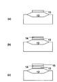
トレンチ型キャパシタの代表的な構造およびその製造方法をP型半導体基板上に形成したキャパシタを例にして、図5(a)〜(c)の製造工程断面図を用いて説明する。
そこで、本発明の目的は、高温熱処理をせずに形成可能であり、かつ、信頼性劣化が少なく、かつ、従来のトレンチキャパシタと同様に、安定した容量値の供給、及び、大容量化が可能な、半導体キャパシタ、及び、その製造方法を提供することである。
まず、第1導電型半導体基板表面に形成された台形状トレンチを有する容量素子形成領域と、前記容量素子領域の台形状トレンチに沿って設けられた第2導電型下部電極層と、少なくとも前記下部電極層の表面に形成された容量絶縁膜と、前記容量絶縁膜の表面に形成された第2導電型上部電極とからなることを特徴とする半導体装置とした。
また、第1導電型半導体基板上にLOCOS法により厚い酸化膜領域と薄い酸化膜領域を形成する工程と、前記厚い酸化膜領域と前記薄い酸化膜領域の酸化膜を前記半導体基板から除去する工程と、前記台形状トレンチの表面に第2導電型不純物を導入して下部電極層を形成する工程と、少なくとも前記下部電極層上に容量絶縁膜を形成する工程と、前記容量絶縁膜上に上部電極となる多結晶シリコン膜を堆積する工程と、前記上部電極となる多結晶シリコンに第2導電型不純物を導入し、所定の形状とすることで上部電極とする工程とからなることを特徴とする半導体装置の製造方法を用いた。
そして、前記容量絶縁膜を形成する工程は、減圧CVDによるシリコン窒化膜形成工程であることを特徴とする半導体装置の製造方法を用いた。
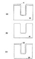
図1(a)〜(c)および図2(d)〜(f)は、本実施の形態の半導体装置、及び、その製造方法を説明するための工程断面図である。本実施の形態では、P型半導体基板を使用した容量素子を例に説明するが、本発明の本質は、基板の導電型、及び、不純物の種類、及び、その導電型に依存しないので、基板の導電型、及び、不純物の種類、及び、その導電型が異なっても同様に実施することが可能である。
まず、図1(a)に示すように、P型不純物(例えばボロン)を添加した抵抗率20Ωcm〜30Ωcmの不純物濃度のP型半導体基板1上に、P型ウェル2を、P型不純物(例えば、ボロン)をドーズ量1×10¹¹〜1×10¹³atoms/cm2でイオン注入、及び、熱処理して拡散させることにより形成する。上記ウェルの有無は、本実施の形態の本質に関係ないので、ウェルを形成しないで容量素子を半導体基板上に直接形成することも可能である。
既存の素子分離技術である、LOCOS(Local Oxidation of Silicon)法とWetエッチングを用いて形成された、LOCOS型トレンチは従来のトレンチと比較して、トレンチの開口部、及び、底部の角は急峻ではないので、角部での電界集中による絶縁破壊等の信頼性劣化を緩和することができる。また、上記LOCOS型トレンチは、トレンチの角を丸くする必要がないため、基板に転移等のダメージを生じさせる原因となる高温での熱処理使わずに、本半導体キャパシタを形成することが可能である。
また、LOCOS型トレンチの数、及び、深さを調整することで大容量化も可能となる。
2 P型ウェル
3 厚い酸化膜
4 容量素子形成領域
5 下部電極層
6 容量絶縁膜
7 上部電極
Claims (5)
- 第1導電型半導体基板と、
前記第1導電型半導体基板の表面に形成された台形状トレンチを有する容量素子形成領域と、
前記容量素子領域の台形状トレンチに沿って前記第1導電型半導体基板の表面近傍に設けられた第2導電型下部電極層と、
前記下部電極層の表面に形成された容量絶縁膜と、
前記容量絶縁膜の表面に形成された第2導電型上部電極と、
からなる半導体装置。 - 前記台形状トレンチは、平行に複数配置されている請求項1記載の半導体装置。
- 第1導電型半導体基板上にLOCOS法により厚い酸化膜領域と薄い酸化膜領域を形成する工程と、
前記厚い酸化膜領域と前記薄い酸化膜領域の酸化膜を前記半導体基板から除去する工程と、
前記台形状トレンチの表面に第2導電型不純物を導入して下部電極層を形成する工程と、
前記下部電極層上に容量絶縁膜を形成する工程と、
前記容量絶縁膜上に上部電極となる多結晶シリコン膜を堆積する工程と、
前記上部電極となる多結晶シリコンに第2導電型不純物を導入し、所定の形状とすることで上部電極とする工程と、
からなる半導体装置の製造方法。 - 前記容量絶縁膜を形成する工程は、熱酸化による酸化膜形成工程である請求項3記載の半導体装置の製造方法。
- 前記容量絶縁膜を形成する工程は、減圧CVDによるシリコン窒化膜形成工程である請求項3記載の半導体装置の製造方法。
Priority Applications (3)
| Application Number | Priority Date | Filing Date | Title |
|---|---|---|---|
| JP2010071085A JP2011204927A (ja) | 2010-03-25 | 2010-03-25 | 半導体装置およびその製造方法 |
| US13/070,267 US8247303B2 (en) | 2010-03-25 | 2011-03-23 | Semiconductor device and method of manufacturing the same |
| US13/552,172 US8710626B2 (en) | 2010-03-25 | 2012-07-18 | Semiconductor device having trapezoidal shaped trenches |
Applications Claiming Priority (1)
| Application Number | Priority Date | Filing Date | Title |
|---|---|---|---|
| JP2010071085A JP2011204927A (ja) | 2010-03-25 | 2010-03-25 | 半導体装置およびその製造方法 |
Publications (2)
| Publication Number | Publication Date |
|---|---|
| JP2011204927A true JP2011204927A (ja) | 2011-10-13 |
| JP2011204927A5 JP2011204927A5 (ja) | 2013-02-28 |
Family
ID=44655415
Family Applications (1)
| Application Number | Title | Priority Date | Filing Date |
|---|---|---|---|
| JP2010071085A Withdrawn JP2011204927A (ja) | 2010-03-25 | 2010-03-25 | 半導体装置およびその製造方法 |
Country Status (2)
| Country | Link |
|---|---|
| US (2) | US8247303B2 (ja) |
| JP (1) | JP2011204927A (ja) |
Cited By (1)
| Publication number | Priority date | Publication date | Assignee | Title |
|---|---|---|---|---|
| WO2019208226A1 (ja) * | 2018-04-27 | 2019-10-31 | 株式会社村田製作所 | キャパシタ |
Families Citing this family (4)
| Publication number | Priority date | Publication date | Assignee | Title |
|---|---|---|---|---|
| CN106298445A (zh) * | 2015-06-26 | 2017-01-04 | 中芯国际集成电路制造(上海)有限公司 | Pip电容器的制作方法、pip电容器及eeprom存储单元 |
| US10056503B2 (en) * | 2016-10-25 | 2018-08-21 | International Business Machines Corporation | MIS capacitor for finned semiconductor structure |
| CN112530933B (zh) * | 2019-09-18 | 2024-03-22 | 铠侠股份有限公司 | 半导体装置 |
| CN111951721B (zh) * | 2020-08-24 | 2021-11-02 | 上海天马微电子有限公司 | 驱动背板、发光面板、显示装置以及成型方法 |
Citations (4)
| Publication number | Priority date | Publication date | Assignee | Title |
|---|---|---|---|---|
| JPH03129769A (ja) * | 1989-05-14 | 1991-06-03 | Texas Instr Inc <Ti> | ダイナミックram記憶素子及び製造方法 |
| JPH0745791A (ja) * | 1993-07-26 | 1995-02-14 | Nec Corp | 半導体装置の製造方法 |
| JP2002222924A (ja) * | 2001-01-25 | 2002-08-09 | Sharp Corp | 半導体装置の製造方法 |
| US6829127B1 (en) * | 2003-03-05 | 2004-12-07 | Altera Corporation | High performance capacitor structure |
Family Cites Families (2)
| Publication number | Priority date | Publication date | Assignee | Title |
|---|---|---|---|---|
| US5111259A (en) * | 1989-07-25 | 1992-05-05 | Texas Instruments Incorporated | Trench capacitor memory cell with curved capacitors |
| JP3396553B2 (ja) | 1994-02-04 | 2003-04-14 | 三菱電機株式会社 | 半導体装置の製造方法及び半導体装置 |
-
2010
- 2010-03-25 JP JP2010071085A patent/JP2011204927A/ja not_active Withdrawn
-
2011
- 2011-03-23 US US13/070,267 patent/US8247303B2/en active Active
-
2012
- 2012-07-18 US US13/552,172 patent/US8710626B2/en not_active Expired - Fee Related
Patent Citations (4)
| Publication number | Priority date | Publication date | Assignee | Title |
|---|---|---|---|---|
| JPH03129769A (ja) * | 1989-05-14 | 1991-06-03 | Texas Instr Inc <Ti> | ダイナミックram記憶素子及び製造方法 |
| JPH0745791A (ja) * | 1993-07-26 | 1995-02-14 | Nec Corp | 半導体装置の製造方法 |
| JP2002222924A (ja) * | 2001-01-25 | 2002-08-09 | Sharp Corp | 半導体装置の製造方法 |
| US6829127B1 (en) * | 2003-03-05 | 2004-12-07 | Altera Corporation | High performance capacitor structure |
Cited By (4)
| Publication number | Priority date | Publication date | Assignee | Title |
|---|---|---|---|---|
| WO2019208226A1 (ja) * | 2018-04-27 | 2019-10-31 | 株式会社村田製作所 | キャパシタ |
| JPWO2019208226A1 (ja) * | 2018-04-27 | 2021-01-07 | 株式会社村田製作所 | キャパシタ |
| JP7052867B2 (ja) | 2018-04-27 | 2022-04-12 | 株式会社村田製作所 | キャパシタ |
| US11488784B2 (en) | 2018-04-27 | 2022-11-01 | Murata Manufacturing Co., Ltd. | Capacitor |
Also Published As
| Publication number | Publication date |
|---|---|
| US20120280359A1 (en) | 2012-11-08 |
| US8247303B2 (en) | 2012-08-21 |
| US8710626B2 (en) | 2014-04-29 |
| US20110233724A1 (en) | 2011-09-29 |
Similar Documents
| Publication | Publication Date | Title |
|---|---|---|
| US8716791B1 (en) | LDMOS with corrugated drift region | |
| TWI549166B (zh) | 在淺溝渠隔離內之隔離電容器 | |
| KR20100121437A (ko) | 반도체 장치 및 그 제조 방법 | |
| US8502326B2 (en) | Gate dielectric formation for high-voltage MOS devices | |
| CN101894741B (zh) | 混合半导体基片的制造方法 | |
| JP5616823B2 (ja) | 半導体装置およびその製造方法 | |
| TWI503983B (zh) | 半導體裝置及其製造方法 | |
| JP2011204927A (ja) | 半導体装置およびその製造方法 | |
| JP5616720B2 (ja) | 半導体装置およびその製造方法 | |
| CN113838906B (zh) | Ldmos晶体管及其制备方法 | |
| JP2010153762A (ja) | 半導体装置およびその製造方法 | |
| JP2006210512A (ja) | 半導体装置、及び、半導体装置の製造方法 | |
| JP2006202850A (ja) | 半導体装置およびその製造方法 | |
| KR101450436B1 (ko) | 반도체 소자의 웰 형성 방법 | |
| TWI662687B (zh) | 半導體裝置及其製造方法 | |
| JP2012038749A (ja) | 半導体装置およびその製造方法 | |
| KR20130124372A (ko) | 반도체 장치, 반도체 장치의 제조 방법 | |
| JP5546298B2 (ja) | 半導体回路装置の製造方法 | |
| JP4673589B2 (ja) | 半導体装置およびその製造方法 | |
| KR100605908B1 (ko) | 반도체 소자 및 그 제조 방법 | |
| JP5071652B2 (ja) | 半導体装置 | |
| US20060115955A1 (en) | Method for manufacturing anti-punch through semiconductor device | |
| KR101099562B1 (ko) | 반도체 소자의 제조방법 | |
| KR20110078930A (ko) | 반도체 소자 및 그 제조 방법 | |
| KR20200025114A (ko) | 반도체 소자의 제조 방법 |
Legal Events
| Date | Code | Title | Description |
|---|---|---|---|
| A521 | Written amendment |
Free format text: JAPANESE INTERMEDIATE CODE: A523 Effective date: 20130116 |
|
| A621 | Written request for application examination |
Free format text: JAPANESE INTERMEDIATE CODE: A621 Effective date: 20130116 |
|
| A977 | Report on retrieval |
Free format text: JAPANESE INTERMEDIATE CODE: A971007 Effective date: 20140131 |
|
| A131 | Notification of reasons for refusal |
Free format text: JAPANESE INTERMEDIATE CODE: A131 Effective date: 20140204 |
|
| A977 | Report on retrieval |
Free format text: JAPANESE INTERMEDIATE CODE: A971007 Effective date: 20140327 |
|
| A761 | Written withdrawal of application |
Free format text: JAPANESE INTERMEDIATE CODE: A761 Effective date: 20140404 |