JP2011204927A - Semiconductor device and manufacturing method of the same - Google Patents
Semiconductor device and manufacturing method of the same Download PDFInfo
- Publication number
- JP2011204927A JP2011204927A JP2010071085A JP2010071085A JP2011204927A JP 2011204927 A JP2011204927 A JP 2011204927A JP 2010071085 A JP2010071085 A JP 2010071085A JP 2010071085 A JP2010071085 A JP 2010071085A JP 2011204927 A JP2011204927 A JP 2011204927A
- Authority
- JP
- Japan
- Prior art keywords
- capacitor
- forming
- insulating film
- trench
- lower electrode
- Prior art date
- Legal status (The legal status is an assumption and is not a legal conclusion. Google has not performed a legal analysis and makes no representation as to the accuracy of the status listed.)
- Withdrawn
Links
- 239000004065 semiconductor Substances 0.000 title claims abstract description 53
- 238000004519 manufacturing process Methods 0.000 title claims abstract description 30
- 239000003990 capacitor Substances 0.000 claims abstract description 62
- 238000000034 method Methods 0.000 claims abstract description 39
- 239000000758 substrate Substances 0.000 claims abstract description 36
- 239000012535 impurity Substances 0.000 claims description 20
- 230000003647 oxidation Effects 0.000 claims description 14
- 238000007254 oxidation reaction Methods 0.000 claims description 14
- 229910021420 polycrystalline silicon Inorganic materials 0.000 claims description 14
- 229910052581 Si3N4 Inorganic materials 0.000 claims description 3
- 238000004518 low pressure chemical vapour deposition Methods 0.000 claims description 3
- HQVNEWCFYHHQES-UHFFFAOYSA-N silicon nitride Chemical compound N12[Si]34N5[Si]62N3[Si]51N64 HQVNEWCFYHHQES-UHFFFAOYSA-N 0.000 claims description 3
- 238000000151 deposition Methods 0.000 claims description 2
- 238000010438 heat treatment Methods 0.000 abstract description 12
- 230000006866 deterioration Effects 0.000 abstract description 5
- 238000001039 wet etching Methods 0.000 abstract description 3
- 230000015572 biosynthetic process Effects 0.000 description 6
- 238000005468 ion implantation Methods 0.000 description 6
- 230000015556 catabolic process Effects 0.000 description 4
- XUIMIQQOPSSXEZ-UHFFFAOYSA-N Silicon Chemical compound [Si] XUIMIQQOPSSXEZ-UHFFFAOYSA-N 0.000 description 3
- 238000005229 chemical vapour deposition Methods 0.000 description 3
- 230000005684 electric field Effects 0.000 description 3
- 238000002955 isolation Methods 0.000 description 3
- 229910021421 monocrystalline silicon Inorganic materials 0.000 description 3
- 230000001590 oxidative effect Effects 0.000 description 3
- 238000000059 patterning Methods 0.000 description 3
- 229910052710 silicon Inorganic materials 0.000 description 3
- 239000010703 silicon Substances 0.000 description 3
- ZOXJGFHDIHLPTG-UHFFFAOYSA-N Boron Chemical compound [B] ZOXJGFHDIHLPTG-UHFFFAOYSA-N 0.000 description 2
- QVGXLLKOCUKJST-UHFFFAOYSA-N atomic oxygen Chemical compound [O] QVGXLLKOCUKJST-UHFFFAOYSA-N 0.000 description 2
- 229910052796 boron Inorganic materials 0.000 description 2
- 229910052760 oxygen Inorganic materials 0.000 description 2
- 239000001301 oxygen Substances 0.000 description 2
- OAICVXFJPJFONN-UHFFFAOYSA-N Phosphorus Chemical compound [P] OAICVXFJPJFONN-UHFFFAOYSA-N 0.000 description 1
- 229910052785 arsenic Inorganic materials 0.000 description 1
- RQNWIZPPADIBDY-UHFFFAOYSA-N arsenic atom Chemical compound [As] RQNWIZPPADIBDY-UHFFFAOYSA-N 0.000 description 1
- 238000006731 degradation reaction Methods 0.000 description 1
- 230000000694 effects Effects 0.000 description 1
- 238000005516 engineering process Methods 0.000 description 1
- 238000007429 general method Methods 0.000 description 1
- 229910052751 metal Inorganic materials 0.000 description 1
- 239000002184 metal Substances 0.000 description 1
- 229910052698 phosphorus Inorganic materials 0.000 description 1
- 239000011574 phosphorus Substances 0.000 description 1
- 230000001681 protective effect Effects 0.000 description 1
Images


Classifications
-
- H—ELECTRICITY
- H01—ELECTRIC ELEMENTS
- H01L—SEMICONDUCTOR DEVICES NOT COVERED BY CLASS H10
- H01L29/00—Semiconductor devices adapted for rectifying, amplifying, oscillating or switching, or capacitors or resistors with at least one potential-jump barrier or surface barrier, e.g. PN junction depletion layer or carrier concentration layer; Details of semiconductor bodies or of electrodes thereof ; Multistep manufacturing processes therefor
- H01L29/66—Types of semiconductor device ; Multistep manufacturing processes therefor
- H01L29/86—Types of semiconductor device ; Multistep manufacturing processes therefor controllable only by variation of the electric current supplied, or only the electric potential applied, to one or more of the electrodes carrying the current to be rectified, amplified, oscillated or switched
- H01L29/92—Capacitors with potential-jump barrier or surface barrier
- H01L29/94—Metal-insulator-semiconductors, e.g. MOS
- H01L29/945—Trench capacitors
-
- H—ELECTRICITY
- H01—ELECTRIC ELEMENTS
- H01L—SEMICONDUCTOR DEVICES NOT COVERED BY CLASS H10
- H01L29/00—Semiconductor devices adapted for rectifying, amplifying, oscillating or switching, or capacitors or resistors with at least one potential-jump barrier or surface barrier, e.g. PN junction depletion layer or carrier concentration layer; Details of semiconductor bodies or of electrodes thereof ; Multistep manufacturing processes therefor
- H01L29/66—Types of semiconductor device ; Multistep manufacturing processes therefor
- H01L29/66007—Multistep manufacturing processes
- H01L29/66075—Multistep manufacturing processes of devices having semiconductor bodies comprising group 14 or group 13/15 materials
- H01L29/66083—Multistep manufacturing processes of devices having semiconductor bodies comprising group 14 or group 13/15 materials the devices being controllable only by variation of the electric current supplied or the electric potential applied, to one or more of the electrodes carrying the current to be rectified, amplified, oscillated or switched, e.g. two-terminal devices
- H01L29/66181—Conductor-insulator-semiconductor capacitors, e.g. trench capacitors
Landscapes
- Engineering & Computer Science (AREA)
- Power Engineering (AREA)
- Microelectronics & Electronic Packaging (AREA)
- Physics & Mathematics (AREA)
- Ceramic Engineering (AREA)
- Condensed Matter Physics & Semiconductors (AREA)
- General Physics & Mathematics (AREA)
- Computer Hardware Design (AREA)
- Manufacturing & Machinery (AREA)
- Semiconductor Integrated Circuits (AREA)
Abstract
Description
本発明は、半導体キャパシタを有する半導体装置およびその製造方法に関する。 The present invention relates to a semiconductor device having a semiconductor capacitor and a method for manufacturing the same.
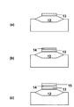
半導体キャパシタは、半導体回路の重要な構成要素の一つで、多種多様なICに組み込まれており、様々な構造の半導体キャパシタが使用されている。従来の半導体キャパシタの一つとして、プレーナー型キャパシタがある。プレーナー型キャパシタの代表的な構造、および、その製造方法を、P型半導体基板上に形成したキャパシタを例に図3(a)〜(c)の製造工程断面図を用いて説明する。 A semiconductor capacitor is one of the important components of a semiconductor circuit and is incorporated in a wide variety of ICs, and semiconductor capacitors having various structures are used. One conventional semiconductor capacitor is a planar capacitor. A typical structure of a planar capacitor and a manufacturing method thereof will be described with reference to manufacturing process cross-sectional views of FIGS. 3A to 3C, taking a capacitor formed on a P-type semiconductor substrate as an example.
まず、図3(a)に示すように、P型半導体基板8表面にN型不純物をイオン注入してから、熱処理することで下部電極層9を形成する。次に、図3(b)に示すように、下部電極層9の表面を熱酸化することで容量絶縁膜10を形成する。次に、図3(c)に示すように、上部電極11となる多結晶シリコン膜を容量絶縁膜10上にCVD等で堆積させ、N型不純物のイオン注入および熱処理を施し、更にパターニングすることによって形成する。以上が、従来のプレーナー型キャパシタの代表的な構造、及び、その製造方法である。プレーナー型キャパシタは、通常使用されるトランジスタの製造工程を利用して低コストで、かつ、簡単に形成できるので、広く使われている。
First, as shown in FIG. 3A, after the N-type impurity is ion-implanted into the surface of the P-
しかし、プレーナー型キャパシタの場合は、入力電圧によっては下部電極層表面の空乏層幅が変化する。空乏層幅が変化することによって容量値も変化してしまい、安定した容量値を得ることができないという弱点を有している。 However, in the case of a planar capacitor, the depletion layer width on the surface of the lower electrode layer changes depending on the input voltage. As the depletion layer width changes, the capacitance value also changes, and there is a weak point that a stable capacitance value cannot be obtained.
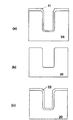
上記弱点を受けて考えられた、従来使用されている半導体キャパシタの一つとして、積層(PIP)型キャパシタがある。上記積層(PIP)型キャパシタの代表的な構造、及びその製造方法をフィールド酸化膜上に形成したキャパシタを例に図4(a)〜(c)の製造工程断面図を用いて説明する。 One of the conventionally used semiconductor capacitors that has been considered in view of the above weak points is a multilayer (PIP) type capacitor. A typical structure of the multilayer (PIP) type capacitor and a method for manufacturing the same will be described with reference to the manufacturing process sectional views of FIGS. 4A to 4C taking a capacitor formed on a field oxide film as an example.
まず、図4(a)に示すように、下部電極13となる多結晶シリコン膜をフィールド酸化膜12上にCVD等で堆積し、多結晶シリコンにN型不純物をイオン注入後、熱処理をし、更にパターニングすることで下部電極13を形成する。次に、図4(b)に示すように、下部電極13上に容量絶縁膜14をCVDで堆積させて形成する。次に、図4(c)に示すように、上部電極15となる多結晶シリコン膜を容量絶縁膜14上にCVD等で堆積させ、N型不純物のイオン注入および熱処理をし、更にパターニングすることによって形成する。以上が、従来の積層(PIP)型キャパシタの代表的な構造、及び、その製造方法である。積層型キャパシタは、上記プレーナー型キャパシタと比較して、下部電極、及び、上部電極に高濃度の不純物が添加されている多結晶シリコンを使用しているので、入力電圧による空乏層幅の変化が少なく、安定した容量値を得ることができる。
First, as shown in FIG. 4A, a polycrystalline silicon film to be the
しかし、上記積層型キャパシタの問題は多結晶シリコン上に形成する容量絶縁膜の形成方法にある。一般的に、多結晶シリコンを熱酸化するときには、高温で酸化を行った方が酸化膜の膜質を良くすることができる。しかし、高温で熱酸化を行うと、酸化工程中の熱によって不純物が拡散してしまい、他の素子(例えば、トランジスタ等)の特性変化および信頼性劣化の原因となりうる。以上の理由から、一般的に、積層(PIP)型キャパシタの容量絶縁膜の形成方法として、比較的低温で酸化膜を形成できるCVD法が採用されている。しかし、CVD法による酸化膜の膜質は、単結晶シリコン上に形成された熱酸化膜と比較すると特性が良くない。そのため、CVD法による酸化膜の膜厚を薄くすることは耐圧劣化や信頼性劣化の原因となるため容量絶縁膜の膜厚を薄くすることができない。その結果、積層(PIP)型キャパシタは、容量値を大きくすることができないという弱点がある。 However, the problem with the multilayer capacitor is in the method of forming a capacitive insulating film formed on polycrystalline silicon. Generally, when polycrystalline silicon is thermally oxidized, the quality of the oxide film can be improved by oxidizing at a high temperature. However, when thermal oxidation is performed at a high temperature, impurities are diffused by heat during the oxidation process, which may cause a change in characteristics of other elements (for example, transistors) and deterioration of reliability. For these reasons, generally, a CVD method capable of forming an oxide film at a relatively low temperature is employed as a method for forming a capacitive insulating film of a multilayer (PIP) type capacitor. However, the quality of the oxide film formed by the CVD method is not as good as that of a thermal oxide film formed on single crystal silicon. For this reason, reducing the thickness of the oxide film by the CVD method causes deterioration in breakdown voltage and reliability, so that the thickness of the capacitor insulating film cannot be reduced. As a result, the multilayer (PIP) type capacitor has a weak point that the capacitance value cannot be increased.
プレーナー型キャパシタや積層型キャパシタの上記弱点を受けて提案された半導体キャパシタの一つとして、トレンチ型キャパシタがある。
トレンチ型キャパシタの代表的な構造およびその製造方法をP型半導体基板上に形成したキャパシタを例にして、図5(a)〜(c)の製造工程断面図を用いて説明する。
As one of the semiconductor capacitors proposed in view of the above weak points of the planar type capacitor and the multilayer type capacitor, there is a trench type capacitor.
A typical structure of a trench capacitor and a method for manufacturing the same will be described with reference to the manufacturing process cross-sectional views of FIGS. 5A to 5C, taking a capacitor formed on a P-type semiconductor substrate as an example.
まず、図5(a)に示すように、トレンチが形成されたP型半導体基板16上に、下部電極となる下部電極層17を、N型不純物をイオン注入、及び、熱処理によって形成する。次に、図5(b)に示すように、下部電極層17が形成されたトレンチ基板表面上に、容量絶縁膜18を、熱酸化によって形成する。次に、図5(c)に示すように、容量絶縁膜18上に上部電極19となる多結晶シリコン膜をCVD等で堆積させ、N型不純物のイオン注入および熱処理をし、更に、パターニングすることで上部電極19を形成する。以上が、従来のトレンチ型キャパシタの代表的な構造、及び、その製造方法である。
First, as shown in FIG. 5A, a
トレンチ型キャパシタは、図5(c)に示すように、下部電極層を複数個のトレンチが形成されているトレンチ基板表面上に形成することによって、下部電極層表面にできる空乏層幅の広がりを、下部電極層濃度、及び、トレンチのアスペクト比や各トレンチ間距離を調整することにより、抑制、または、制限することができる。その結果、プレーナー型キャパシタで問題となっている入力電圧の変化による、容量値の変化を抑制することができる。また、トレンチ型キャパシタは、単結晶シリコン基板上に容量絶縁膜を形成するので、熱酸化による酸化膜の形成が可能となり、膜厚を薄くすることができる。そのため、容量値を大きくすることが可能となり、積層型キャパシタよりも有利となる。更に、トレンチのアスペクト比や数を調整することで大容量化が可能である。 As shown in FIG. 5C, the trench capacitor has a lower depletion layer width that can be formed on the surface of the lower electrode layer by forming the lower electrode layer on the surface of the trench substrate on which a plurality of trenches are formed. It can be suppressed or restricted by adjusting the lower electrode layer concentration, the trench aspect ratio, and the distance between the trenches. As a result, it is possible to suppress a change in capacitance value due to a change in input voltage, which is a problem with a planar capacitor. In addition, since the capacitor of the trench type capacitor is formed on the single crystal silicon substrate, an oxide film can be formed by thermal oxidation, and the film thickness can be reduced. Therefore, it is possible to increase the capacitance value, which is more advantageous than the multilayer capacitor. Furthermore, the capacity can be increased by adjusting the aspect ratio and the number of trenches.
しかし、トレンチ型キャパシタは、トレンチの開口部、及び、底部が角張っている。そのため、トレンチ上に形成した、容量絶縁膜、及び、上部電極の多結晶シリコンの膜厚が、トレンチの開口部、及び、底部の角で膜厚が薄くなってしまう。その結果、トレンチ型キャパシタは、膜厚が薄くなるトレンチの開口部、及び、底部の角で、電界集中による絶縁破壊を生じやすくなり、信頼性が低下するという弱点がある。 However, the trench type capacitor has a square opening and bottom. Therefore, the film thickness of the capacitor insulating film and the polycrystalline silicon of the upper electrode formed on the trench becomes thin at the opening and bottom corners of the trench. As a result, the trench capacitor has a weak point in that it tends to cause dielectric breakdown due to electric field concentration at the opening and bottom corners of the trench where the film thickness is reduced, and the reliability is lowered.
上記弱点を受けて、トレンチの開口部、及び、底部を丸くする方法を提案されている(例えば、特許文献1参照)。トレンチの開口部、及び、底部を丸くする方法を図6(a)〜(c)に示した工程断面図を用いて説明する。特許文献1では、トレンチ基板上に、MOSFETを形成する場合が記載されているが、ソース、及び、ドレイン領域の形成過程を省略し、ゲート酸化膜を容量絶縁膜に置き換えることによって、上記トレンチの開口部、及び、底部を丸くする方法を適用することができると考えられる。
In response to the above weak points, a method of rounding the opening and bottom of the trench has been proposed (see, for example, Patent Document 1). A method for rounding the opening and bottom of the trench will be described with reference to the process cross-sectional views shown in FIGS.
半導体基板20表面を酸化した後、部分的に基板表面の酸化膜を除去し、次いで、半導体基板20にトレンチを設ける。その後、熱酸化してトレンチ内に犠牲酸化膜21を形成した時の断面が図6(a)に示されている。次いで、図6(b)に示すように、上記犠牲酸化膜21を除去する。そして、図6(c)に示すように、上記犠牲酸化膜21を除去した半導体基板表面に、酸化膜22(特許文献の場合はゲート酸化膜)を、1000℃以上(例えば1215℃)の酸素雰囲気に熱酸化を施すことによって形成する。
After oxidizing the surface of the
特許文献1によれば、トレンチを形成した後、1000℃以上の酸素雰囲気で熱酸化を行って酸化膜を形成し、そして、熱酸化によって形成した酸化膜を除去する工程を、1〜2回繰り返すことにより、トレンチの開口部、及び、底部を丸くすることができる。トレンチの開口部、及び、底部を丸くすることによって、トレンチの角で生じる電界集中を回避することができる。
According to
しかし、上記の方法では、トレンチの開口部、及び、底部を丸くするために、1000℃以上という高温の酸素雰囲気で、酸化膜を形成、及び、除去する工程が1〜2回必要とするが、高温での熱処理は、基板に転移等のダメージが生じやすくなってしまうという課題を有している。また、高温での熱処理は、すでに形成してある不純物層の再分布を引き起こすため、濃度のばらつきを増大させる可能性が高くなるという課題もある。
そこで、本発明の目的は、高温熱処理をせずに形成可能であり、かつ、信頼性劣化が少なく、かつ、従来のトレンチキャパシタと同様に、安定した容量値の供給、及び、大容量化が可能な、半導体キャパシタ、及び、その製造方法を提供することである。
However, in the above method, in order to round the opening and bottom of the trench, the process of forming and removing the oxide film in an oxygen atmosphere at a high temperature of 1000 ° C. or more is required once or twice. The heat treatment at a high temperature has a problem that damage such as transfer is likely to occur on the substrate. In addition, since heat treatment at a high temperature causes redistribution of the impurity layer that has already been formed, there is a problem that the possibility of increasing the variation in concentration becomes high.
Therefore, the object of the present invention is that it can be formed without high-temperature heat treatment, has little deterioration in reliability, and can provide a stable capacitance value and increase the capacitance as in the conventional trench capacitor. It is possible to provide a semiconductor capacitor and a method for manufacturing the same.
本発明では、上記目的を達成するために、次の手段を用いた。
まず、第1導電型半導体基板表面に形成された台形状トレンチを有する容量素子形成領域と、前記容量素子領域の台形状トレンチに沿って設けられた第2導電型下部電極層と、少なくとも前記下部電極層の表面に形成された容量絶縁膜と、前記容量絶縁膜の表面に形成された第2導電型上部電極とからなることを特徴とする半導体装置とした。
In the present invention, the following means are used to achieve the above object.
First, a capacitive element forming region having a trapezoidal trench formed on the surface of the first conductive type semiconductor substrate, a second conductive type lower electrode layer provided along the trapezoidal trench in the capacitive element region, and at least the lower part A semiconductor device is characterized by comprising a capacitive insulating film formed on the surface of the electrode layer and a second conductivity type upper electrode formed on the surface of the capacitive insulating film.
また、前記台形状トレンチは、複数であることを特徴とする半導体装置とした。
また、第1導電型半導体基板上にLOCOS法により厚い酸化膜領域と薄い酸化膜領域を形成する工程と、前記厚い酸化膜領域と前記薄い酸化膜領域の酸化膜を前記半導体基板から除去する工程と、前記台形状トレンチの表面に第2導電型不純物を導入して下部電極層を形成する工程と、少なくとも前記下部電極層上に容量絶縁膜を形成する工程と、前記容量絶縁膜上に上部電極となる多結晶シリコン膜を堆積する工程と、前記上部電極となる多結晶シリコンに第2導電型不純物を導入し、所定の形状とすることで上部電極とする工程とからなることを特徴とする半導体装置の製造方法を用いた。
Further, the semiconductor device is characterized in that a plurality of the trapezoidal trenches are provided.
A step of forming a thick oxide film region and a thin oxide film region on the first conductivity type semiconductor substrate by a LOCOS method; and a step of removing the oxide film of the thick oxide film region and the thin oxide film region from the semiconductor substrate. A step of introducing a second conductivity type impurity into the surface of the trapezoidal trench to form a lower electrode layer; a step of forming a capacitive insulating film on at least the lower electrode layer; and an upper portion on the capacitive insulating film A step of depositing a polycrystalline silicon film serving as an electrode, and a step of introducing a second conductivity type impurity into the polycrystalline silicon serving as the upper electrode to obtain a predetermined shape, thereby forming the upper electrode. The manufacturing method of the semiconductor device to be used was used.
また、前記容量絶縁膜を形成する工程は、熱酸化による酸化膜形成工程であることを特徴とする半導体装置の製造方法を用いた。
そして、前記容量絶縁膜を形成する工程は、減圧CVDによるシリコン窒化膜形成工程であることを特徴とする半導体装置の製造方法を用いた。
In addition, a method of manufacturing a semiconductor device is used, wherein the step of forming the capacitor insulating film is a step of forming an oxide film by thermal oxidation.
Then, the semiconductor device manufacturing method is characterized in that the step of forming the capacitive insulating film is a step of forming a silicon nitride film by low pressure CVD.
本発明によれば、既存の素子分離技術であるLOCOS(Local Oxidation of Silicon)法を応用し、LOCOS型トレンチ基板を形成することによって、高温熱処理をせずに形成でき、かつ、信頼性劣化が少なく、かつ、従来のトレンチキャパシタと同様に、安定した容量値の供給、及び、大容量化が可能な、半導体キャパシタ、及び、その製造方法を提供することができる。 According to the present invention, by applying the LOCOS (Local Oxidation of Silicon) method, which is an existing element isolation technique, and forming a LOCOS type trench substrate, it can be formed without high-temperature heat treatment, and reliability degradation is reduced. It is possible to provide a semiconductor capacitor and a method for manufacturing the semiconductor capacitor that can supply a stable capacitance value and increase the capacitance, as in the case of a conventional trench capacitor.
以下、本発明の実施の形態について詳細に説明する。
図1(a)〜(c)および図2(d)〜(f)は、本実施の形態の半導体装置、及び、その製造方法を説明するための工程断面図である。本実施の形態では、P型半導体基板を使用した容量素子を例に説明するが、本発明の本質は、基板の導電型、及び、不純物の種類、及び、その導電型に依存しないので、基板の導電型、及び、不純物の種類、及び、その導電型が異なっても同様に実施することが可能である。
Hereinafter, embodiments of the present invention will be described in detail.
FIGS. 1A to 1C and FIGS. 2D to 2F are process cross-sectional views for explaining the semiconductor device of this embodiment and the manufacturing method thereof. In this embodiment, a capacitive element using a P-type semiconductor substrate will be described as an example. However, since the essence of the present invention does not depend on the conductivity type of the substrate, the type of impurities, and the conductivity type, the substrate Even if the conductivity type, the type of impurities, and the conductivity type are different, the present invention can be implemented in the same manner.
以下、本実施の形態を、図1(a)〜(c)および図2(d)〜(f)に示す工程断面図を用いて、本実施の形態の半導体装置の構造、及び、その製造方法を説明する。
まず、図1(a)に示すように、P型不純物(例えばボロン)を添加した抵抗率20Ωcm〜30Ωcmの不純物濃度のP型半導体基板1上に、P型ウェル2を、P型不純物(例えば、ボロン)をドーズ量1×10¹¹〜1×10¹³atoms/cm2でイオン注入、及び、熱処理して拡散させることにより形成する。上記ウェルの有無は、本実施の形態の本質に関係ないので、ウェルを形成しないで容量素子を半導体基板上に直接形成することも可能である。
Hereinafter, the structure of the semiconductor device of this embodiment and its manufacture will be described with reference to the process cross-sectional views shown in FIGS. 1 (a) to 1 (c) and FIGS. 2 (d) to (f). A method will be described.
First, as shown in FIG. 1A, a P-
次に、図1(b)に示すように、上記P型ウェル2の形成された基板表面の一部に、既存の素子分離技術であるLOCOS法を用いて、厚い酸化膜3を0.2mm〜4.0mmの膜厚で熱酸化することで形成し、厚い酸化膜領域と薄い酸化膜領域を平行に隣接して設ける。このとき、厚い酸化膜3が形成されない領域(薄い酸化膜領域)の数、及び、その間隔の大きさは製造する容量素子の容量、及び、空乏層幅の広がりを抑制する程度に合わせて決定する。
Next, as shown in FIG. 1B, a
次に、図1(c)に示すように、Wetエッチングにより表面の酸化膜を全て除去して、シリコン基板表面に、複数の台形状のLOCOSトレンチ型の容量素子形成領域4を形成する。 Next, as shown in FIG. 1C, all oxide films on the surface are removed by wet etching, and a plurality of trapezoidal LOCOS trench type capacitive element formation regions 4 are formed on the surface of the silicon substrate.
次に、図2(d)に示すように、下部電極層5を、高濃度のN型不純物(例えば、砒素)をドーズ量5×10¹³〜1×10¹⁵ atoms/cm2で容量素子形成領域の基板表面にイオン注入することによって形成する。このとき、下部電極層5は半導体基板1上に形成されたP型ウェル2表面の容量素子形成領域4に、半導体基板表面の台形状のトレンチに沿って設けられる。
Next, as shown in FIG. 2D, the
次に、図2(e)に示すように容量絶縁膜6となる酸化膜を、下部電極層5の表面に熱酸化により、例えば、膜厚数十nm〜1μmとなるように形成する。容量絶縁膜6は熱酸化膜に限ることはなく、シリコン窒化膜であっても良いが、その場合は台形状トレンチ表面を一様に覆うように減圧CVDによる成膜が好ましい。
Next, as shown in FIG. 2E, an oxide film that becomes the capacitive insulating
次に、図2(f)に示すように、容量素子の上部電極7を、容量絶縁膜6表面に多結晶シリコンを堆積させ、N型不純物(例えば、リン)をドーズ量1×10¹⁵〜1016 atoms/cm2でイオン注入し、パターニングによって形成する。なお、不純物導入工程は、イオン注入の代わりにプリデポジションで行っても良い。上部電極7を形成した後の、電極配線以降(金属配線や保護膜の形成過程)の工程は、一般的な半導体装置の製造方法と同様であるので、詳細な説明は割愛する。以上が、本実施の形態の半導体装置の構造、及び、その製造方法である。
Next, as shown in FIG. 2F, the upper electrode 7 of the capacitive element is deposited on the surface of the capacitive insulating
以上に説明した、本実施の形態により次のような効果を得ることができる。
既存の素子分離技術である、LOCOS(Local Oxidation of Silicon)法とWetエッチングを用いて形成された、LOCOS型トレンチは従来のトレンチと比較して、トレンチの開口部、及び、底部の角は急峻ではないので、角部での電界集中による絶縁破壊等の信頼性劣化を緩和することができる。また、上記LOCOS型トレンチは、トレンチの角を丸くする必要がないため、基板に転移等のダメージを生じさせる原因となる高温での熱処理使わずに、本半導体キャパシタを形成することが可能である。
The following effects can be obtained by the present embodiment described above.
The LOCOS-type trench formed by using the LOCOS (Local Oxidation of Silicon) method and wet etching, which are existing element isolation technologies, has a sharper opening and bottom corner than the conventional trench. Therefore, reliability deterioration such as dielectric breakdown due to electric field concentration at the corner can be mitigated. In addition, since the LOCOS-type trench does not require round corners of the trench, it is possible to form the semiconductor capacitor without using a heat treatment at a high temperature that causes damage such as dislocation in the substrate. .
また、下部電極層濃度、及び、上記LOCOS型トレンチの間隔を調整することによって、入力電圧による空乏層幅の変化を抑えることができ、その結果、安定した容量値を得ることができる。 Further, by adjusting the lower electrode layer concentration and the interval between the LOCOS trenches, a change in the depletion layer width due to the input voltage can be suppressed, and as a result, a stable capacitance value can be obtained.
更に、容量絶縁膜は単結晶シリコン基板上に形成するので、膜質の良い熱酸化膜の使用が可能なので、膜厚を薄くでき、積層(PIP)型と比較して容量を大きくすることが可能となる。
また、LOCOS型トレンチの数、及び、深さを調整することで大容量化も可能となる。
Furthermore, since the capacitor insulating film is formed on a single crystal silicon substrate, it is possible to use a thermal oxide film with good film quality, so that the film thickness can be reduced and the capacity can be increased as compared with the stacked (PIP) type. It becomes.
Further, the capacity can be increased by adjusting the number and depth of the LOCOS type trenches.
1 P型半導体基板
2 P型ウェル
3 厚い酸化膜
4 容量素子形成領域
5 下部電極層
6 容量絶縁膜
7 上部電極
1 P-type semiconductor substrate 2 P-type well 3 Thick oxide film 4 Capacitor
Claims (5)
前記第1導電型半導体基板の表面に形成された台形状トレンチを有する容量素子形成領域と、
前記容量素子領域の台形状トレンチに沿って前記第1導電型半導体基板の表面近傍に設けられた第2導電型下部電極層と、
前記下部電極層の表面に形成された容量絶縁膜と、
前記容量絶縁膜の表面に形成された第2導電型上部電極と、
からなる半導体装置。 A first conductivity type semiconductor substrate;
A capacitor element forming region having a trapezoidal trench formed on the surface of the first conductive type semiconductor substrate;
A second conductivity type lower electrode layer provided near the surface of the first conductivity type semiconductor substrate along the trapezoidal trench in the capacitor element region;
A capacitive insulating film formed on the surface of the lower electrode layer;
A second conductivity type upper electrode formed on the surface of the capacitive insulating film;
A semiconductor device comprising:
前記厚い酸化膜領域と前記薄い酸化膜領域の酸化膜を前記半導体基板から除去する工程と、
前記台形状トレンチの表面に第2導電型不純物を導入して下部電極層を形成する工程と、
前記下部電極層上に容量絶縁膜を形成する工程と、
前記容量絶縁膜上に上部電極となる多結晶シリコン膜を堆積する工程と、
前記上部電極となる多結晶シリコンに第2導電型不純物を導入し、所定の形状とすることで上部電極とする工程と、
からなる半導体装置の製造方法。 Forming a thick oxide film region and a thin oxide film region on the first conductivity type semiconductor substrate by a LOCOS method;
Removing the thick oxide region and the oxide region of the thin oxide region from the semiconductor substrate;
Introducing a second conductivity type impurity into the surface of the trapezoidal trench to form a lower electrode layer;
Forming a capacitive insulating film on the lower electrode layer;
Depositing a polycrystalline silicon film to be an upper electrode on the capacitive insulating film;
Introducing a second conductivity type impurity into polycrystalline silicon to be the upper electrode and forming the upper electrode by making a predetermined shape;
A method for manufacturing a semiconductor device comprising:
Priority Applications (3)
| Application Number | Priority Date | Filing Date | Title |
|---|---|---|---|
| JP2010071085A JP2011204927A (en) | 2010-03-25 | 2010-03-25 | Semiconductor device and manufacturing method of the same |
| US13/070,267 US8247303B2 (en) | 2010-03-25 | 2011-03-23 | Semiconductor device and method of manufacturing the same |
| US13/552,172 US8710626B2 (en) | 2010-03-25 | 2012-07-18 | Semiconductor device having trapezoidal shaped trenches |
Applications Claiming Priority (1)
| Application Number | Priority Date | Filing Date | Title |
|---|---|---|---|
| JP2010071085A JP2011204927A (en) | 2010-03-25 | 2010-03-25 | Semiconductor device and manufacturing method of the same |
Publications (2)
| Publication Number | Publication Date |
|---|---|
| JP2011204927A true JP2011204927A (en) | 2011-10-13 |
| JP2011204927A5 JP2011204927A5 (en) | 2013-02-28 |
Family
ID=44655415
Family Applications (1)
| Application Number | Title | Priority Date | Filing Date |
|---|---|---|---|
| JP2010071085A Withdrawn JP2011204927A (en) | 2010-03-25 | 2010-03-25 | Semiconductor device and manufacturing method of the same |
Country Status (2)
| Country | Link |
|---|---|
| US (2) | US8247303B2 (en) |
| JP (1) | JP2011204927A (en) |
Cited By (1)
| Publication number | Priority date | Publication date | Assignee | Title |
|---|---|---|---|---|
| WO2019208226A1 (en) * | 2018-04-27 | 2019-10-31 | 株式会社村田製作所 | Capacitor |
Families Citing this family (4)
| Publication number | Priority date | Publication date | Assignee | Title |
|---|---|---|---|---|
| CN106298445A (en) * | 2015-06-26 | 2017-01-04 | 中芯国际集成电路制造(上海)有限公司 | The manufacture method of PIP capacitor device, PIP capacitor device and EEPROM memory cell |
| US10056503B2 (en) * | 2016-10-25 | 2018-08-21 | International Business Machines Corporation | MIS capacitor for finned semiconductor structure |
| CN112530933B (en) * | 2019-09-18 | 2024-03-22 | 铠侠股份有限公司 | Semiconductor device with a semiconductor device having a plurality of semiconductor chips |
| CN111951721B (en) * | 2020-08-24 | 2021-11-02 | 上海天马微电子有限公司 | Driving back plate, light-emitting panel, display device and forming method |
Citations (4)
| Publication number | Priority date | Publication date | Assignee | Title |
|---|---|---|---|---|
| JPH03129769A (en) * | 1989-05-14 | 1991-06-03 | Texas Instr Inc <Ti> | Dynamic ram storge element and its manufacture |
| JPH0745791A (en) * | 1993-07-26 | 1995-02-14 | Nec Corp | Manufacture of semiconductor device |
| JP2002222924A (en) * | 2001-01-25 | 2002-08-09 | Sharp Corp | Manufacturing method for semiconductor device |
| US6829127B1 (en) * | 2003-03-05 | 2004-12-07 | Altera Corporation | High performance capacitor structure |
Family Cites Families (2)
| Publication number | Priority date | Publication date | Assignee | Title |
|---|---|---|---|---|
| US5111259A (en) * | 1989-07-25 | 1992-05-05 | Texas Instruments Incorporated | Trench capacitor memory cell with curved capacitors |
| JP3396553B2 (en) | 1994-02-04 | 2003-04-14 | 三菱電機株式会社 | Semiconductor device manufacturing method and semiconductor device |
-
2010
- 2010-03-25 JP JP2010071085A patent/JP2011204927A/en not_active Withdrawn
-
2011
- 2011-03-23 US US13/070,267 patent/US8247303B2/en active Active
-
2012
- 2012-07-18 US US13/552,172 patent/US8710626B2/en not_active Expired - Fee Related
Patent Citations (4)
| Publication number | Priority date | Publication date | Assignee | Title |
|---|---|---|---|---|
| JPH03129769A (en) * | 1989-05-14 | 1991-06-03 | Texas Instr Inc <Ti> | Dynamic ram storge element and its manufacture |
| JPH0745791A (en) * | 1993-07-26 | 1995-02-14 | Nec Corp | Manufacture of semiconductor device |
| JP2002222924A (en) * | 2001-01-25 | 2002-08-09 | Sharp Corp | Manufacturing method for semiconductor device |
| US6829127B1 (en) * | 2003-03-05 | 2004-12-07 | Altera Corporation | High performance capacitor structure |
Cited By (4)
| Publication number | Priority date | Publication date | Assignee | Title |
|---|---|---|---|---|
| WO2019208226A1 (en) * | 2018-04-27 | 2019-10-31 | 株式会社村田製作所 | Capacitor |
| JPWO2019208226A1 (en) * | 2018-04-27 | 2021-01-07 | 株式会社村田製作所 | Capacitor |
| JP7052867B2 (en) | 2018-04-27 | 2022-04-12 | 株式会社村田製作所 | Capacitor |
| US11488784B2 (en) | 2018-04-27 | 2022-11-01 | Murata Manufacturing Co., Ltd. | Capacitor |
Also Published As
| Publication number | Publication date |
|---|---|
| US8710626B2 (en) | 2014-04-29 |
| US8247303B2 (en) | 2012-08-21 |
| US20110233724A1 (en) | 2011-09-29 |
| US20120280359A1 (en) | 2012-11-08 |
Similar Documents
| Publication | Publication Date | Title |
|---|---|---|
| US8716791B1 (en) | LDMOS with corrugated drift region | |
| TWI549166B (en) | Isolated capacitors within shallow trench isolation | |
| KR20100121437A (en) | Semiconductor device and method of manufacturing the same | |
| US8502326B2 (en) | Gate dielectric formation for high-voltage MOS devices | |
| CN101894741B (en) | Fabrication process of a hybrid semiconductor substrate | |
| JP5616823B2 (en) | Semiconductor device and manufacturing method thereof | |
| TWI503983B (en) | Power mosfet and methods for forming the same | |
| JP2011204927A (en) | Semiconductor device and manufacturing method of the same | |
| JP5616720B2 (en) | Semiconductor device and manufacturing method thereof | |
| CN113838906B (en) | LDMOS transistor and preparation method thereof | |
| JP2010153762A (en) | Semiconductor device and method of manufacturing the same | |
| JP2006210512A (en) | Semiconductor device and its manufacturing method | |
| JP2006202850A (en) | Semiconductor device and its manufacturing method | |
| KR101450436B1 (en) | Method for forming well of semiconductor device | |
| TWI662687B (en) | Semiconductor device and manufacturing method thereof | |
| JP2012038749A (en) | Semiconductor device and method of manufacturing the same | |
| KR20130124372A (en) | Semiconductor device, and method for manufacturing semiconductor device | |
| JP5546298B2 (en) | Manufacturing method of semiconductor circuit device | |
| JP4673589B2 (en) | Semiconductor device and manufacturing method thereof | |
| KR100605908B1 (en) | Semiconductor Device And Method For Manufacturing The Same | |
| JP5071652B2 (en) | Semiconductor device | |
| US20060115955A1 (en) | Method for manufacturing anti-punch through semiconductor device | |
| KR101099562B1 (en) | Method for manufacturing of semiconductor device | |
| KR20110078930A (en) | A semicondutor device and a method of manufacturing the same | |
| KR20200025114A (en) | Method of manufacturing semiconductor devices |
Legal Events
| Date | Code | Title | Description |
|---|---|---|---|
| A521 | Written amendment |
Free format text: JAPANESE INTERMEDIATE CODE: A523 Effective date: 20130116 |
|
| A621 | Written request for application examination |
Free format text: JAPANESE INTERMEDIATE CODE: A621 Effective date: 20130116 |
|
| A977 | Report on retrieval |
Free format text: JAPANESE INTERMEDIATE CODE: A971007 Effective date: 20140131 |
|
| A131 | Notification of reasons for refusal |
Free format text: JAPANESE INTERMEDIATE CODE: A131 Effective date: 20140204 |
|
| A977 | Report on retrieval |
Free format text: JAPANESE INTERMEDIATE CODE: A971007 Effective date: 20140327 |
|
| A761 | Written withdrawal of application |
Free format text: JAPANESE INTERMEDIATE CODE: A761 Effective date: 20140404 |