JP2011180583A - 液晶表示装置 - Google Patents
液晶表示装置 Download PDFInfo
- Publication number
- JP2011180583A JP2011180583A JP2011021175A JP2011021175A JP2011180583A JP 2011180583 A JP2011180583 A JP 2011180583A JP 2011021175 A JP2011021175 A JP 2011021175A JP 2011021175 A JP2011021175 A JP 2011021175A JP 2011180583 A JP2011180583 A JP 2011180583A
- Authority
- JP
- Japan
- Prior art keywords
- pixel electrode
- insulating layer
- liquid crystal
- electrode
- pixel
- Prior art date
- Legal status (The legal status is an assumption and is not a legal conclusion. Google has not performed a legal analysis and makes no representation as to the accuracy of the status listed.)
- Withdrawn
Links
Images


Classifications
-
- G—PHYSICS
- G02—OPTICS
- G02F—OPTICAL DEVICES OR ARRANGEMENTS FOR THE CONTROL OF LIGHT BY MODIFICATION OF THE OPTICAL PROPERTIES OF THE MEDIA OF THE ELEMENTS INVOLVED THEREIN; NON-LINEAR OPTICS; FREQUENCY-CHANGING OF LIGHT; OPTICAL LOGIC ELEMENTS; OPTICAL ANALOGUE/DIGITAL CONVERTERS
- G02F1/00—Devices or arrangements for the control of the intensity, colour, phase, polarisation or direction of light arriving from an independent light source, e.g. switching, gating or modulating; Non-linear optics
- G02F1/01—Devices or arrangements for the control of the intensity, colour, phase, polarisation or direction of light arriving from an independent light source, e.g. switching, gating or modulating; Non-linear optics for the control of the intensity, phase, polarisation or colour
- G02F1/13—Devices or arrangements for the control of the intensity, colour, phase, polarisation or direction of light arriving from an independent light source, e.g. switching, gating or modulating; Non-linear optics for the control of the intensity, phase, polarisation or colour based on liquid crystals, e.g. single liquid crystal display cells
- G02F1/133—Constructional arrangements; Operation of liquid crystal cells; Circuit arrangements
- G02F1/1333—Constructional arrangements; Manufacturing methods
- G02F1/1343—Electrodes
- G02F1/134309—Electrodes characterised by their geometrical arrangement
-
- G—PHYSICS
- G02—OPTICS
- G02F—OPTICAL DEVICES OR ARRANGEMENTS FOR THE CONTROL OF LIGHT BY MODIFICATION OF THE OPTICAL PROPERTIES OF THE MEDIA OF THE ELEMENTS INVOLVED THEREIN; NON-LINEAR OPTICS; FREQUENCY-CHANGING OF LIGHT; OPTICAL LOGIC ELEMENTS; OPTICAL ANALOGUE/DIGITAL CONVERTERS
- G02F1/00—Devices or arrangements for the control of the intensity, colour, phase, polarisation or direction of light arriving from an independent light source, e.g. switching, gating or modulating; Non-linear optics
- G02F1/01—Devices or arrangements for the control of the intensity, colour, phase, polarisation or direction of light arriving from an independent light source, e.g. switching, gating or modulating; Non-linear optics for the control of the intensity, phase, polarisation or colour
- G02F1/13—Devices or arrangements for the control of the intensity, colour, phase, polarisation or direction of light arriving from an independent light source, e.g. switching, gating or modulating; Non-linear optics for the control of the intensity, phase, polarisation or colour based on liquid crystals, e.g. single liquid crystal display cells
- G02F1/133—Constructional arrangements; Operation of liquid crystal cells; Circuit arrangements
- G02F1/136—Liquid crystal cells structurally associated with a semi-conducting layer or substrate, e.g. cells forming part of an integrated circuit
- G02F1/1362—Active matrix addressed cells
- G02F1/136227—Through-hole connection of the pixel electrode to the active element through an insulation layer
-
- G—PHYSICS
- G02—OPTICS
- G02F—OPTICAL DEVICES OR ARRANGEMENTS FOR THE CONTROL OF LIGHT BY MODIFICATION OF THE OPTICAL PROPERTIES OF THE MEDIA OF THE ELEMENTS INVOLVED THEREIN; NON-LINEAR OPTICS; FREQUENCY-CHANGING OF LIGHT; OPTICAL LOGIC ELEMENTS; OPTICAL ANALOGUE/DIGITAL CONVERTERS
- G02F1/00—Devices or arrangements for the control of the intensity, colour, phase, polarisation or direction of light arriving from an independent light source, e.g. switching, gating or modulating; Non-linear optics
- G02F1/01—Devices or arrangements for the control of the intensity, colour, phase, polarisation or direction of light arriving from an independent light source, e.g. switching, gating or modulating; Non-linear optics for the control of the intensity, phase, polarisation or colour
- G02F1/13—Devices or arrangements for the control of the intensity, colour, phase, polarisation or direction of light arriving from an independent light source, e.g. switching, gating or modulating; Non-linear optics for the control of the intensity, phase, polarisation or colour based on liquid crystals, e.g. single liquid crystal display cells
- G02F1/133—Constructional arrangements; Operation of liquid crystal cells; Circuit arrangements
- G02F1/1333—Constructional arrangements; Manufacturing methods
- G02F1/133345—Insulating layers
-
- G—PHYSICS
- G02—OPTICS
- G02F—OPTICAL DEVICES OR ARRANGEMENTS FOR THE CONTROL OF LIGHT BY MODIFICATION OF THE OPTICAL PROPERTIES OF THE MEDIA OF THE ELEMENTS INVOLVED THEREIN; NON-LINEAR OPTICS; FREQUENCY-CHANGING OF LIGHT; OPTICAL LOGIC ELEMENTS; OPTICAL ANALOGUE/DIGITAL CONVERTERS
- G02F1/00—Devices or arrangements for the control of the intensity, colour, phase, polarisation or direction of light arriving from an independent light source, e.g. switching, gating or modulating; Non-linear optics
- G02F1/01—Devices or arrangements for the control of the intensity, colour, phase, polarisation or direction of light arriving from an independent light source, e.g. switching, gating or modulating; Non-linear optics for the control of the intensity, phase, polarisation or colour
- G02F1/13—Devices or arrangements for the control of the intensity, colour, phase, polarisation or direction of light arriving from an independent light source, e.g. switching, gating or modulating; Non-linear optics for the control of the intensity, phase, polarisation or colour based on liquid crystals, e.g. single liquid crystal display cells
- G02F1/133—Constructional arrangements; Operation of liquid crystal cells; Circuit arrangements
- G02F1/1333—Constructional arrangements; Manufacturing methods
- G02F1/1343—Electrodes
- G02F1/13439—Electrodes characterised by their electrical, optical, physical properties; materials therefor; method of making
-
- G—PHYSICS
- G02—OPTICS
- G02F—OPTICAL DEVICES OR ARRANGEMENTS FOR THE CONTROL OF LIGHT BY MODIFICATION OF THE OPTICAL PROPERTIES OF THE MEDIA OF THE ELEMENTS INVOLVED THEREIN; NON-LINEAR OPTICS; FREQUENCY-CHANGING OF LIGHT; OPTICAL LOGIC ELEMENTS; OPTICAL ANALOGUE/DIGITAL CONVERTERS
- G02F1/00—Devices or arrangements for the control of the intensity, colour, phase, polarisation or direction of light arriving from an independent light source, e.g. switching, gating or modulating; Non-linear optics
- G02F1/01—Devices or arrangements for the control of the intensity, colour, phase, polarisation or direction of light arriving from an independent light source, e.g. switching, gating or modulating; Non-linear optics for the control of the intensity, phase, polarisation or colour
- G02F1/13—Devices or arrangements for the control of the intensity, colour, phase, polarisation or direction of light arriving from an independent light source, e.g. switching, gating or modulating; Non-linear optics for the control of the intensity, phase, polarisation or colour based on liquid crystals, e.g. single liquid crystal display cells
- G02F1/133—Constructional arrangements; Operation of liquid crystal cells; Circuit arrangements
- G02F1/136—Liquid crystal cells structurally associated with a semi-conducting layer or substrate, e.g. cells forming part of an integrated circuit
- G02F1/1362—Active matrix addressed cells
- G02F1/1368—Active matrix addressed cells in which the switching element is a three-electrode device
Abstract
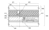
【解決手段】液晶表示装置の画素電極の端部を、隣接する画素電極の端部に絶縁層を挟んで重ねて設け、隣接する画素間にある間隙を狭め、画素に占める表示領域の割合を高めればよい。
【選択図】図4
Description
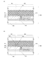
本実施の形態では、絶縁層を間に挟んで、液晶表示装置の画素電極の端部を隣接する画素電極の端部に重ねて設ける構成を、図1を用いて説明する。また、その作製方法を、図2を用いて説明する。
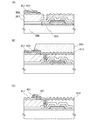
本実施の形態では、3つ以上の隣接する画素電極を有する表示装置において、絶縁層を挟んで、互いの端部を重ねて設ける構成について図3、乃至図7を用いて説明する。
本実施の形態では、実施の形態1及び実施の形態2で例示した画素電極を有し、さらにフォトセンサとしてフォトダイオードを同一基板上に設ける液晶表示装置について、図8乃至図10を用いて説明する。
本実施の形態では、絶縁層を間に挟んで、画素電極の端部を隣接する画素電極の端部に重ねて設ける構成を有し、当該画素電極、並びにフォトセンサを同一基板上に有する液晶表示装置について、その駆動方法について説明する。
本実施の形態では、カラーフィルタを設け、フルカラー表示が可能な液晶表示モジュールとする一例を示す。
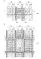
本実施の形態は、実施の形態1乃至3で説明した液晶表示装置に用いる酸化物半導体層を含むトランジスタ、及び作製方法の一例を、図18を用いて詳細に説明する。上記実施の形態と同一部分又は同様な機能を有する部分、及び工程は、上記実施の形態と同様に行うことができ、繰り返しの説明は省略する。また同じ箇所の詳細な説明は省略する。
本実施の形態においては、上記実施の形態で説明した液晶表示装置を具備する電子機器の例について説明する。
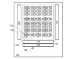
101 画素回路
103 画素
104 画素
105 表示素子
106 フォトセンサ
107 表示素子駆動回路
108 表示素子駆動回路
109 回路
110 フォトセンサ駆動回路
115 カラーフィルタ
116a FPC(フレキシブルプリントサーキット)
120 表示パネル
125 表示素子
135 光
139 外光
190 液晶表示モジュール
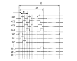
201 トランジスタ
202 保持容量
203 液晶素子
204 フォトダイオード
205 トランジスタ
206 トランジスタ
207 ゲート信号線
208 フォトダイオードリセット信号線
209 信号線
210 ビデオデータ信号線
211 フォトセンサ出力信号線
212 フォトセンサ基準信号線
213 ゲート信号線
214 容量配線
221 トランジスタ
222 保持容量
223 液晶素子
224 容量配線
227 ゲート信号線
230 基板
231 絶縁層
232 ゲート絶縁層
233 酸化物半導体層
234 電極層
235 電極層
237 絶縁層
238 p層
239 i層
240 n層
241 絶縁層
242 反射電極層
243 接続電極層
244 配向膜
245 凹部
251 電極層
252 電極層
253 酸化物半導体層
254 電極層
255 酸化物半導体層
256 酸化物半導体層
257 電極層
258 電極層
259 電極層
300 基板
307 絶縁層
308 絶縁層
340 レジストマスク
340a レジストマスク
340b レジストマスク
350 トランジスタ
350B トランジスタ
350G トランジスタ
350R トランジスタ
370 絶縁層
403 対向電極
404 配向膜
405 液晶層
408 対向基板
411 画素電極
411a 画素電極
411b 画素電極
412 画素電極
413 画素電極
414 配向膜
421 絶縁層
422 絶縁層
431 絶縁層
441 スペーサ
450 液晶表示装置
451 画素
452 画素
453 画素
460 液晶表示装置
461 画素
462 画素
470 液晶表示装置
471 画素
472 画素
480 液晶表示装置
490 液晶表示装置
505 基板
506 保護絶縁層
507 ゲート絶縁層
510 トランジスタ
511 ゲート電極層
512 ゲート信号線G
515a ソース電極層
515b ドレイン電極層
516 絶縁層
530 酸化物半導体膜
531 酸化物半導体層
1032 表示部
9630 筐体
9631 表示部
9632 操作キー
9633 太陽電池
9634 充放電制御回路
9635 バッテリー
9636 コンバータ
9637 コンバータ
Claims (8)
- 絶縁層と、
それぞれ独立したスイッチング素子とそれぞれ電気的に接続する第1の画素電極及び第2の画素電極と、
前記第1の画素電極及び前記第2の画素電極に対向する対向電極と、
前記第1の画素電極及び前記第2の画素電極と対向電極の間に液晶層を有し、
前記第2の画素電極の端部が、前記絶縁層を介して前記第1の画素電極の端部の上に重ねて設けられている液晶表示装置。 - さらに着色された絶縁層を有し、前記着色された絶縁層は前記第2の画素電極の端部から延在して第1の画素電極の上面に重なる請求項1記載の液晶表示装置。
- 前記着色された絶縁層が前記第1の画素電極の上面に重なる前記第2の画素電極の側面を覆う請求項2記載の液晶表示装置。
- 前記スイッチング素子に、酸化物半導体を有するトランジスタを用いる請求項1乃至請求項3のいずれかに記載の液晶表示装置。
- 第1の絶縁層と、第2の絶縁層と、
それぞれ独立したスイッチング素子とそれぞれ電気的に接続する第1の画素電極、第2の画素電極及び第3の画素電極と、
前記第1の画素電極、前記第2の画素電極及び前記第3の画素電極に対向する対向電極と、
前記第1の画素電極、前記第2の画素電極及び前記第3の画素電極と対向電極の間に液晶層を有し、
前記スイッチング素子に酸化物半導体を有するトランジスタを用い、
前記第2の画素電極を挟んで、第1の画素電極と、第2の画素電極と、第3の画素電極は隣接し、
前記第2の画素電極の一方の端部が、前記第1の絶縁層を介して前記第1の画素電極の端部の上に重ねて設けられ、
前記第2の画素電極の他方の端部が、前記第2の絶縁層を介して前記第3の画素電極の端部の下に重ねて設けられている液晶表示装置。 - 第1の絶縁層と、第2の絶縁層と、
それぞれ独立したスイッチング素子とそれぞれ電気的に接続する第1の画素電極、第2の画素電極及び第3の画素電極と、
前記第1の画素電極、前記第2の画素電極及び前記第3の画素電極に対向する対向電極と、
前記第1の画素電極、前記第2の画素電極及び前記第3の画素電極と対向電極の間に液晶層を有し、
前記スイッチング素子に酸化物半導体を有するトランジスタを用い、
前記第2の画素電極を挟んで、第1の画素電極と、第2の画素電極と、第3の画素電極は隣接し、
前記第2の画素電極の一方の端部が、前記第1の絶縁層を介して前記第1の画素電極の端部の上に重ねて設けられ、
前記第2の画素電極の他方の端部が、前記第2の絶縁層を介して前記第3の画素電極の端部の上に重ねて設けられている、液晶表示装置。 - 第1の絶縁層と、第2の絶縁層と、
それぞれ独立したスイッチング素子とそれぞれ電気的に接続する第1の画素電極、第2の画素電極及び第3の画素電極と、
前記第1の画素電極、前記第2の画素電極及び前記第3の画素電極に対向する対向電極と、
前記第1の画素電極、前記第2の画素電極及び前記第3の画素電極と対向電極の間に液晶層を有し、
前記スイッチング素子に酸化物半導体を有するトランジスタを用い、
前記第2の画素電極を挟んで、第1の画素電極と、第2の画素電極と、第3の画素電極は隣接し、
前記第2の画素電極の一方の端部が、前記第1の絶縁層を介して前記第1の画素電極の端部の下に重ねて設けられ、
前記第2の画素電極の他方の端部が、前記第2の絶縁層を介して前記第3の画素電極の端部の下に重ねて設けられている、液晶表示装置。 - 前記酸化物半導体を有するトランジスタと電気的に接続するフォトセンサと、
前記画素電極を同一基板上に有し、
前記フォトセンサを囲うブラックマトリクスを有する請求項5乃至請求項7のいずれかに記載の液晶表示装置。
Priority Applications (1)
| Application Number | Priority Date | Filing Date | Title |
|---|---|---|---|
| JP2011021175A JP2011180583A (ja) | 2010-02-05 | 2011-02-02 | 液晶表示装置 |
Applications Claiming Priority (3)
| Application Number | Priority Date | Filing Date | Title |
|---|---|---|---|
| JP2010024643 | 2010-02-05 | ||
| JP2010024643 | 2010-02-05 | ||
| JP2011021175A JP2011180583A (ja) | 2010-02-05 | 2011-02-02 | 液晶表示装置 |
Related Child Applications (1)
| Application Number | Title | Priority Date | Filing Date |
|---|---|---|---|
| JP2014087062A Division JP2014167641A (ja) | 2010-02-05 | 2014-04-21 | 表示装置 |
Publications (2)
| Publication Number | Publication Date |
|---|---|
| JP2011180583A true JP2011180583A (ja) | 2011-09-15 |
| JP2011180583A5 JP2011180583A5 (ja) | 2013-12-12 |
Family
ID=44353466
Family Applications (4)
| Application Number | Title | Priority Date | Filing Date |
|---|---|---|---|
| JP2011021175A Withdrawn JP2011180583A (ja) | 2010-02-05 | 2011-02-02 | 液晶表示装置 |
| JP2014087062A Withdrawn JP2014167641A (ja) | 2010-02-05 | 2014-04-21 | 表示装置 |
| JP2015196353A Active JP6025948B2 (ja) | 2010-02-05 | 2015-10-02 | 表示装置の作製方法 |
| JP2016199788A Active JP6317412B2 (ja) | 2010-02-05 | 2016-10-11 | 表示装置及び表示装置の作製方法 |
Family Applications After (3)
| Application Number | Title | Priority Date | Filing Date |
|---|---|---|---|
| JP2014087062A Withdrawn JP2014167641A (ja) | 2010-02-05 | 2014-04-21 | 表示装置 |
| JP2015196353A Active JP6025948B2 (ja) | 2010-02-05 | 2015-10-02 | 表示装置の作製方法 |
| JP2016199788A Active JP6317412B2 (ja) | 2010-02-05 | 2016-10-11 | 表示装置及び表示装置の作製方法 |
Country Status (4)
| Country | Link |
|---|---|
| US (2) | US9057918B2 (ja) |
| JP (4) | JP2011180583A (ja) |
| TW (2) | TWI522705B (ja) |
| WO (1) | WO2011096276A1 (ja) |
Cited By (5)
| Publication number | Priority date | Publication date | Assignee | Title |
|---|---|---|---|---|
| JP2016006503A (ja) * | 2014-05-28 | 2016-01-14 | 株式会社半導体エネルギー研究所 | 液晶表示装置及び電子機器 |
| JP2016177284A (ja) * | 2015-03-19 | 2016-10-06 | 株式会社半導体エネルギー研究所 | 液晶表示装置及び該液晶表示装置を用いた電子機器 |
| JP2017224294A (ja) * | 2016-06-10 | 2017-12-21 | 株式会社半導体エネルギー研究所 | 情報端末 |
| KR20170142228A (ko) * | 2016-06-16 | 2017-12-28 | 삼성디스플레이 주식회사 | 표시 장치 및 이의 제조 방법 |
| JP2021009200A (ja) * | 2019-06-28 | 2021-01-28 | スタンレー電気株式会社 | 液晶素子、照明装置 |
Families Citing this family (14)
| Publication number | Priority date | Publication date | Assignee | Title |
|---|---|---|---|---|
| WO2011145537A1 (en) | 2010-05-21 | 2011-11-24 | Semiconductor Energy Laboratory Co., Ltd. | Liquid crystal display device |
| KR101995919B1 (ko) | 2013-01-30 | 2019-07-04 | 삼성디스플레이 주식회사 | 액정 표시 장치 |
| CN106463080B (zh) * | 2014-06-13 | 2019-08-20 | 株式会社半导体能源研究所 | 显示装置 |
| US9722090B2 (en) | 2014-06-23 | 2017-08-01 | Semiconductor Energy Laboratory Co., Ltd. | Semiconductor device including first gate oxide semiconductor film, and second gate |
| US9461179B2 (en) * | 2014-07-11 | 2016-10-04 | Semiconductor Energy Laboratory Co., Ltd. | Thin film transistor device (TFT) comprising stacked oxide semiconductor layers and having a surrounded channel structure |
| JP6702760B2 (ja) * | 2016-02-25 | 2020-06-03 | 株式会社ジャパンディスプレイ | 表示装置 |
| JP6723080B2 (ja) * | 2016-06-08 | 2020-07-15 | 三菱電機株式会社 | 液晶表示装置 |
| US10955950B2 (en) | 2016-11-09 | 2021-03-23 | Semiconductor Energy Laboratory Co., Ltd. | Display device, display module, electronic device, and method for manufacturing the display device |
| US10330993B2 (en) | 2016-12-23 | 2019-06-25 | Semiconductor Energy Laboratory Co., Ltd. | Display device |
| KR102541393B1 (ko) * | 2017-11-30 | 2023-06-09 | 삼성전자주식회사 | 디스플레이 장치 |
| KR20200066500A (ko) * | 2018-11-30 | 2020-06-10 | 삼성디스플레이 주식회사 | 표시장치 |
| CN109801926B (zh) * | 2019-01-17 | 2022-01-21 | 惠科股份有限公司 | 薄膜晶体管基板及其制备方法、显示装置 |
| CN111880343B (zh) * | 2020-08-27 | 2022-04-05 | 豪威半导体(上海)有限责任公司 | 硅基液晶器件以及硅基液晶显示面板 |
| CN112068346A (zh) * | 2020-09-28 | 2020-12-11 | 成都中电熊猫显示科技有限公司 | 阵列基板以及液晶显示面板 |
Citations (5)
| Publication number | Priority date | Publication date | Assignee | Title |
|---|---|---|---|---|
| JPH05216071A (ja) * | 1992-02-03 | 1993-08-27 | Seiko Instr Inc | 光弁用基板 |
| JPH06160875A (ja) * | 1992-11-20 | 1994-06-07 | Seiko Epson Corp | 液晶表示装置 |
| JPH1144893A (ja) * | 1997-04-18 | 1999-02-16 | Hyundai Electron Ind Co Ltd | 液晶表示装置及びその製造方法 |
| JP2007250982A (ja) * | 2006-03-17 | 2007-09-27 | Canon Inc | 酸化物半導体を用いた薄膜トランジスタ及び表示装置 |
| JP2009134041A (ja) * | 2007-11-30 | 2009-06-18 | Sony Corp | 表示装置 |
Family Cites Families (34)
| Publication number | Priority date | Publication date | Assignee | Title |
|---|---|---|---|---|
| JPH0217721A (ja) | 1988-07-05 | 1990-01-22 | Sharp Corp | 論理回路 |
| JPH0217721U (ja) | 1988-07-21 | 1990-02-06 | ||
| JP2653559B2 (ja) | 1991-02-20 | 1997-09-17 | シャープ株式会社 | 単純マトリクス液晶表示装置 |
| JPH07152023A (ja) | 1993-10-04 | 1995-06-16 | Matsushita Electric Ind Co Ltd | 表示パネルおよびそれを用いた表示装置 |
| DE4435450A1 (de) | 1993-10-04 | 1995-04-06 | Matsushita Electric Ind Co Ltd | Flüssigkristalleinheit und Projektionsanzeige unter Verwendung einer Flüssigkristalleinheit |
| JPH07152033A (ja) | 1993-11-26 | 1995-06-16 | Asahi Glass Co Ltd | 液晶表示素子 |
| US5673127A (en) | 1993-12-01 | 1997-09-30 | Matsushita Electric Industrial Co., Ltd. | Display panel and display device using a display panel |
| US6545653B1 (en) | 1994-07-14 | 2003-04-08 | Matsushita Electric Industrial Co., Ltd. | Method and device for displaying image signals and viewfinder |
| JP3195172B2 (ja) * | 1994-09-21 | 2001-08-06 | アルプス電気株式会社 | 液晶表示素子およびその製造方法 |
| US5936685A (en) | 1995-02-28 | 1999-08-10 | Nec Corporation | Liquid crystal display device with pixel electrode overlapping drain wiring |
| JPH08297301A (ja) | 1995-02-28 | 1996-11-12 | Nec Corp | 液晶表示装置 |
| US6404472B1 (en) * | 1995-09-08 | 2002-06-11 | Alejandro Andreatta | Film containing oriented dye, method of manufacturing the same, and polarizer and liquid crystal display unit utilizing the same |
| JPH10123564A (ja) | 1996-10-16 | 1998-05-15 | Seiko Epson Corp | 液晶パネル及び投射型表示装置 |
| JP3776187B2 (ja) | 1996-12-06 | 2006-05-17 | シャープ株式会社 | 液晶表示装置及びその製造方法 |
| JP3390633B2 (ja) | 1997-07-14 | 2003-03-24 | 株式会社半導体エネルギー研究所 | 半導体装置の作製方法 |
| US6839108B1 (en) * | 1998-05-16 | 2005-01-04 | Semiconductor Energy Laboratory Co., Ltd. | Liquid crystal display device and method of manufacturing the same |
| JP4138077B2 (ja) | 1998-06-02 | 2008-08-20 | 株式会社半導体エネルギー研究所 | 反射型の液晶表示装置及び電子機器 |
| JP4223094B2 (ja) | 1998-06-12 | 2009-02-12 | 株式会社半導体エネルギー研究所 | 電気光学表示装置 |
| JP2000002872A (ja) | 1998-06-16 | 2000-01-07 | Semiconductor Energy Lab Co Ltd | 液晶表示装置およびその作製方法 |
| US6233033B1 (en) * | 1999-03-29 | 2001-05-15 | National Semiconductor Corp. | Pixel array for LC silicon light valve featuring pixels with overlapping edges |
| JP3702859B2 (ja) * | 2001-04-16 | 2005-10-05 | セイコーエプソン株式会社 | 電気光学装置及び電子機器 |
| JP2004029386A (ja) | 2002-06-26 | 2004-01-29 | Sharp Corp | 表示パネルおよびその製造方法 |
| JP2005062589A (ja) | 2003-08-18 | 2005-03-10 | Toshiba Matsushita Display Technology Co Ltd | 液晶表示装置 |
| KR101200444B1 (ko) * | 2005-07-14 | 2012-11-12 | 삼성디스플레이 주식회사 | 박막트랜지스터와 이를 이용한 박막트랜지스터 기판 및 그제조방법 및 액정표시장치 |
| TWI335455B (en) * | 2005-09-22 | 2011-01-01 | Ind Tech Res Inst | Liquid crystal display device |
| JP5064747B2 (ja) | 2005-09-29 | 2012-10-31 | 株式会社半導体エネルギー研究所 | 半導体装置、電気泳動表示装置、表示モジュール、電子機器、及び半導体装置の作製方法 |
| EP1995787A3 (en) | 2005-09-29 | 2012-01-18 | Semiconductor Energy Laboratory Co, Ltd. | Semiconductor device having oxide semiconductor layer and manufacturing method therof |
| JP4752499B2 (ja) * | 2005-12-26 | 2011-08-17 | セイコーエプソン株式会社 | 反射型液晶表示基板の製造方法及び反射型液晶表示装置の製造方法 |
| US7821613B2 (en) | 2005-12-28 | 2010-10-26 | Semiconductor Energy Laboratory Co., Ltd. | Display device and manufacturing method thereof |
| JP4981358B2 (ja) * | 2006-05-15 | 2012-07-18 | キヤノン株式会社 | 反射型液晶表示装置及びその製造方法 |
| KR101282403B1 (ko) * | 2006-09-19 | 2013-07-04 | 삼성디스플레이 주식회사 | 액정표시장치 |
| JP5046810B2 (ja) | 2007-09-05 | 2012-10-10 | 株式会社リコー | 現像装置および画像形成装置 |
| JP4407732B2 (ja) | 2007-09-05 | 2010-02-03 | ソニー株式会社 | 液晶表示装置 |
| JP2009069422A (ja) | 2007-09-12 | 2009-04-02 | Sony Corp | 液晶表示素子および投射型液晶表示装置 |
-
2011
- 2011-01-13 WO PCT/JP2011/050906 patent/WO2011096276A1/en active Application Filing
- 2011-01-27 US US13/015,183 patent/US9057918B2/en active Active
- 2011-01-31 TW TW100103656A patent/TWI522705B/zh not_active IP Right Cessation
- 2011-01-31 TW TW104140541A patent/TWI576643B/zh not_active IP Right Cessation
- 2011-02-02 JP JP2011021175A patent/JP2011180583A/ja not_active Withdrawn
-
2014
- 2014-04-21 JP JP2014087062A patent/JP2014167641A/ja not_active Withdrawn
-
2015
- 2015-06-03 US US14/729,097 patent/US9541803B2/en active Active
- 2015-10-02 JP JP2015196353A patent/JP6025948B2/ja active Active
-
2016
- 2016-10-11 JP JP2016199788A patent/JP6317412B2/ja active Active
Patent Citations (5)
| Publication number | Priority date | Publication date | Assignee | Title |
|---|---|---|---|---|
| JPH05216071A (ja) * | 1992-02-03 | 1993-08-27 | Seiko Instr Inc | 光弁用基板 |
| JPH06160875A (ja) * | 1992-11-20 | 1994-06-07 | Seiko Epson Corp | 液晶表示装置 |
| JPH1144893A (ja) * | 1997-04-18 | 1999-02-16 | Hyundai Electron Ind Co Ltd | 液晶表示装置及びその製造方法 |
| JP2007250982A (ja) * | 2006-03-17 | 2007-09-27 | Canon Inc | 酸化物半導体を用いた薄膜トランジスタ及び表示装置 |
| JP2009134041A (ja) * | 2007-11-30 | 2009-06-18 | Sony Corp | 表示装置 |
Cited By (12)
| Publication number | Priority date | Publication date | Assignee | Title |
|---|---|---|---|---|
| JP2016006503A (ja) * | 2014-05-28 | 2016-01-14 | 株式会社半導体エネルギー研究所 | 液晶表示装置及び電子機器 |
| JP2019079080A (ja) * | 2014-05-28 | 2019-05-23 | 株式会社半導体エネルギー研究所 | 半導体装置 |
| JP2016177284A (ja) * | 2015-03-19 | 2016-10-06 | 株式会社半導体エネルギー研究所 | 液晶表示装置及び該液晶表示装置を用いた電子機器 |
| US9612499B2 (en) | 2015-03-19 | 2017-04-04 | Semiconductor Energy Laboratory Co., Ltd. | Liquid crystal display device and electronic device using liquid crystal display device |
| JP2020106849A (ja) * | 2015-03-19 | 2020-07-09 | 株式会社半導体エネルギー研究所 | 半導体装置 |
| JP2022058383A (ja) * | 2015-03-19 | 2022-04-12 | 株式会社半導体エネルギー研究所 | 表示装置 |
| JP2017224294A (ja) * | 2016-06-10 | 2017-12-21 | 株式会社半導体エネルギー研究所 | 情報端末 |
| JP2021131561A (ja) * | 2016-06-10 | 2021-09-09 | 株式会社半導体エネルギー研究所 | 情報端末 |
| KR20170142228A (ko) * | 2016-06-16 | 2017-12-28 | 삼성디스플레이 주식회사 | 표시 장치 및 이의 제조 방법 |
| KR102523971B1 (ko) * | 2016-06-16 | 2023-04-21 | 삼성디스플레이 주식회사 | 표시 장치 및 이의 제조 방법 |
| JP2021009200A (ja) * | 2019-06-28 | 2021-01-28 | スタンレー電気株式会社 | 液晶素子、照明装置 |
| JP7345293B2 (ja) | 2019-06-28 | 2023-09-15 | スタンレー電気株式会社 | 液晶素子、照明装置 |
Also Published As
| Publication number | Publication date |
|---|---|
| US20110194059A1 (en) | 2011-08-11 |
| JP6025948B2 (ja) | 2016-11-16 |
| US20150261047A1 (en) | 2015-09-17 |
| US9541803B2 (en) | 2017-01-10 |
| WO2011096276A1 (en) | 2011-08-11 |
| JP6317412B2 (ja) | 2018-04-25 |
| JP2017016156A (ja) | 2017-01-19 |
| TWI522705B (zh) | 2016-02-21 |
| TWI576643B (zh) | 2017-04-01 |
| JP2015232737A (ja) | 2015-12-24 |
| US9057918B2 (en) | 2015-06-16 |
| JP2014167641A (ja) | 2014-09-11 |
| TW201610533A (zh) | 2016-03-16 |
| TW201142444A (en) | 2011-12-01 |
Similar Documents
| Publication | Publication Date | Title |
|---|---|---|
| JP6317412B2 (ja) | 表示装置及び表示装置の作製方法 | |
| JP6538099B2 (ja) | 電子機器 | |
| TWI597712B (zh) | 半導體顯示裝置及其驅動方法 | |
| JP6022526B2 (ja) | 半導体装置 | |
| JP2022078055A (ja) | 半導体装置 | |
| US9147706B2 (en) | Semiconductor device having sensor circuit having amplifier circuit | |
| JP2014240983A (ja) | 表示装置 |
Legal Events
| Date | Code | Title | Description |
|---|---|---|---|
| A521 | Request for written amendment filed |
Free format text: JAPANESE INTERMEDIATE CODE: A523 Effective date: 20131024 |
|
| A621 | Written request for application examination |
Free format text: JAPANESE INTERMEDIATE CODE: A621 Effective date: 20131024 |
|
| A871 | Explanation of circumstances concerning accelerated examination |
Free format text: JAPANESE INTERMEDIATE CODE: A871 Effective date: 20131024 |
|
| A975 | Report on accelerated examination |
Free format text: JAPANESE INTERMEDIATE CODE: A971005 Effective date: 20131119 |
|
| A131 | Notification of reasons for refusal |
Free format text: JAPANESE INTERMEDIATE CODE: A131 Effective date: 20140121 |
|
| A521 | Request for written amendment filed |
Free format text: JAPANESE INTERMEDIATE CODE: A523 Effective date: 20140128 |
|
| A02 | Decision of refusal |
Free format text: JAPANESE INTERMEDIATE CODE: A02 Effective date: 20140401 |
|
| A761 | Written withdrawal of application |
Free format text: JAPANESE INTERMEDIATE CODE: A761 Effective date: 20140421 |