JP2011164591A - 半導体装置及び電子機器 - Google Patents
半導体装置及び電子機器 Download PDFInfo
- Publication number
- JP2011164591A JP2011164591A JP2011000549A JP2011000549A JP2011164591A JP 2011164591 A JP2011164591 A JP 2011164591A JP 2011000549 A JP2011000549 A JP 2011000549A JP 2011000549 A JP2011000549 A JP 2011000549A JP 2011164591 A JP2011164591 A JP 2011164591A
- Authority
- JP
- Japan
- Prior art keywords
- signal line
- transistor
- period
- source
- nth
- Prior art date
- Legal status (The legal status is an assumption and is not a legal conclusion. Google has not performed a legal analysis and makes no representation as to the accuracy of the status listed.)
- Withdrawn
Links
- 239000004065 semiconductor Substances 0.000 title claims abstract description 148
- 230000015572 biosynthetic process Effects 0.000 claims abstract description 27
- 239000011159 matrix material Substances 0.000 abstract description 16
- 230000008878 coupling Effects 0.000 abstract description 9
- 238000010168 coupling process Methods 0.000 abstract description 9
- 238000005859 coupling reaction Methods 0.000 abstract description 9
- 239000010410 layer Substances 0.000 description 205
- 239000010408 film Substances 0.000 description 77
- 239000000758 substrate Substances 0.000 description 46
- 238000000034 method Methods 0.000 description 41
- 238000010438 heat treatment Methods 0.000 description 36
- XKRFYHLGVUSROY-UHFFFAOYSA-N Argon Chemical compound [Ar] XKRFYHLGVUSROY-UHFFFAOYSA-N 0.000 description 30
- 239000007789 gas Substances 0.000 description 27
- 239000000463 material Substances 0.000 description 26
- 238000004544 sputter deposition Methods 0.000 description 26
- IJGRMHOSHXDMSA-UHFFFAOYSA-N Atomic nitrogen Chemical compound N#N IJGRMHOSHXDMSA-UHFFFAOYSA-N 0.000 description 19
- 229910052760 oxygen Inorganic materials 0.000 description 19
- QVGXLLKOCUKJST-UHFFFAOYSA-N atomic oxygen Chemical compound [O] QVGXLLKOCUKJST-UHFFFAOYSA-N 0.000 description 18
- 239000001301 oxygen Substances 0.000 description 18
- 230000008569 process Effects 0.000 description 17
- 229910007541 Zn O Inorganic materials 0.000 description 15
- 229910052786 argon Inorganic materials 0.000 description 15
- 229910052710 silicon Inorganic materials 0.000 description 15
- XUIMIQQOPSSXEZ-UHFFFAOYSA-N Silicon Chemical compound [Si] XUIMIQQOPSSXEZ-UHFFFAOYSA-N 0.000 description 14
- 230000006870 function Effects 0.000 description 14
- 239000010703 silicon Substances 0.000 description 14
- 238000005530 etching Methods 0.000 description 13
- 239000001257 hydrogen Substances 0.000 description 13
- 229910052739 hydrogen Inorganic materials 0.000 description 13
- XAGFODPZIPBFFR-UHFFFAOYSA-N aluminium Chemical compound [Al] XAGFODPZIPBFFR-UHFFFAOYSA-N 0.000 description 12
- 239000010936 titanium Substances 0.000 description 12
- UFHFLCQGNIYNRP-UHFFFAOYSA-N Hydrogen Chemical compound [H][H] UFHFLCQGNIYNRP-UHFFFAOYSA-N 0.000 description 11
- 229910052581 Si3N4 Inorganic materials 0.000 description 11
- 239000012298 atmosphere Substances 0.000 description 11
- 239000010949 copper Substances 0.000 description 11
- HQVNEWCFYHHQES-UHFFFAOYSA-N silicon nitride Chemical compound N12[Si]34N5[Si]62N3[Si]51N64 HQVNEWCFYHHQES-UHFFFAOYSA-N 0.000 description 11
- GQPLMRYTRLFLPF-UHFFFAOYSA-N Nitrous Oxide Chemical compound [O-][N+]#N GQPLMRYTRLFLPF-UHFFFAOYSA-N 0.000 description 10
- 229910052782 aluminium Inorganic materials 0.000 description 10
- 238000004519 manufacturing process Methods 0.000 description 10
- 229910052751 metal Inorganic materials 0.000 description 10
- 239000002184 metal Substances 0.000 description 10
- 238000005070 sampling Methods 0.000 description 10
- RTAQQCXQSZGOHL-UHFFFAOYSA-N Titanium Chemical compound [Ti] RTAQQCXQSZGOHL-UHFFFAOYSA-N 0.000 description 9
- 229910052802 copper Inorganic materials 0.000 description 9
- 229910052757 nitrogen Inorganic materials 0.000 description 9
- 238000000206 photolithography Methods 0.000 description 9
- 229910052719 titanium Inorganic materials 0.000 description 9
- RYGMFSIKBFXOCR-UHFFFAOYSA-N Copper Chemical compound [Cu] RYGMFSIKBFXOCR-UHFFFAOYSA-N 0.000 description 8
- XLOMVQKBTHCTTD-UHFFFAOYSA-N Zinc monoxide Chemical compound [Zn]=O XLOMVQKBTHCTTD-UHFFFAOYSA-N 0.000 description 8
- 239000011521 glass Substances 0.000 description 8
- 230000001681 protective effect Effects 0.000 description 8
- VYPSYNLAJGMNEJ-UHFFFAOYSA-N silicon dioxide Inorganic materials O=[Si]=O VYPSYNLAJGMNEJ-UHFFFAOYSA-N 0.000 description 8
- ZOKXTWBITQBERF-UHFFFAOYSA-N Molybdenum Chemical compound [Mo] ZOKXTWBITQBERF-UHFFFAOYSA-N 0.000 description 7
- 125000004429 atom Chemical group 0.000 description 7
- 239000011651 chromium Substances 0.000 description 7
- 239000012535 impurity Substances 0.000 description 7
- 229910052750 molybdenum Inorganic materials 0.000 description 7
- 239000011733 molybdenum Substances 0.000 description 7
- 229910052814 silicon oxide Inorganic materials 0.000 description 7
- 230000018044 dehydration Effects 0.000 description 6
- 238000006297 dehydration reaction Methods 0.000 description 6
- 238000006356 dehydrogenation reaction Methods 0.000 description 6
- 238000005268 plasma chemical vapour deposition Methods 0.000 description 6
- 238000009832 plasma treatment Methods 0.000 description 6
- 229910052721 tungsten Inorganic materials 0.000 description 6
- 239000010937 tungsten Substances 0.000 description 6
- XLYOFNOQVPJJNP-UHFFFAOYSA-N water Substances O XLYOFNOQVPJJNP-UHFFFAOYSA-N 0.000 description 6
- 229910001868 water Inorganic materials 0.000 description 6
- 239000000956 alloy Substances 0.000 description 5
- 239000001307 helium Substances 0.000 description 5
- 229910052734 helium Inorganic materials 0.000 description 5
- SWQJXJOGLNCZEY-UHFFFAOYSA-N helium atom Chemical compound [He] SWQJXJOGLNCZEY-UHFFFAOYSA-N 0.000 description 5
- 239000001272 nitrous oxide Substances 0.000 description 5
- 230000003071 parasitic effect Effects 0.000 description 5
- 239000002356 single layer Substances 0.000 description 5
- 229910052715 tantalum Inorganic materials 0.000 description 5
- GUVRBAGPIYLISA-UHFFFAOYSA-N tantalum atom Chemical compound [Ta] GUVRBAGPIYLISA-UHFFFAOYSA-N 0.000 description 5
- WFKWXMTUELFFGS-UHFFFAOYSA-N tungsten Chemical compound [W] WFKWXMTUELFFGS-UHFFFAOYSA-N 0.000 description 5
- 239000011701 zinc Substances 0.000 description 5
- QGZKDVFQNNGYKY-UHFFFAOYSA-N Ammonia Chemical compound N QGZKDVFQNNGYKY-UHFFFAOYSA-N 0.000 description 4
- VYZAMTAEIAYCRO-UHFFFAOYSA-N Chromium Chemical compound [Cr] VYZAMTAEIAYCRO-UHFFFAOYSA-N 0.000 description 4
- BLRPTPMANUNPDV-UHFFFAOYSA-N Silane Chemical compound [SiH4] BLRPTPMANUNPDV-UHFFFAOYSA-N 0.000 description 4
- 229910045601 alloy Inorganic materials 0.000 description 4
- 239000000460 chlorine Substances 0.000 description 4
- 229910052804 chromium Inorganic materials 0.000 description 4
- 238000004891 communication Methods 0.000 description 4
- 238000010586 diagram Methods 0.000 description 4
- KPUWHANPEXNPJT-UHFFFAOYSA-N disiloxane Chemical class [SiH3]O[SiH3] KPUWHANPEXNPJT-UHFFFAOYSA-N 0.000 description 4
- 229910052738 indium Inorganic materials 0.000 description 4
- 229910044991 metal oxide Inorganic materials 0.000 description 4
- 150000004706 metal oxides Chemical class 0.000 description 4
- 239000000203 mixture Substances 0.000 description 4
- 229910021421 monocrystalline silicon Inorganic materials 0.000 description 4
- -1 polyethylene terephthalate Polymers 0.000 description 4
- 238000001552 radio frequency sputter deposition Methods 0.000 description 4
- 229910000077 silane Inorganic materials 0.000 description 4
- 239000011787 zinc oxide Substances 0.000 description 4
- QTBSBXVTEAMEQO-UHFFFAOYSA-N Acetic acid Chemical compound CC(O)=O QTBSBXVTEAMEQO-UHFFFAOYSA-N 0.000 description 3
- ZAMOUSCENKQFHK-UHFFFAOYSA-N Chlorine atom Chemical compound [Cl] ZAMOUSCENKQFHK-UHFFFAOYSA-N 0.000 description 3
- 229910052779 Neodymium Inorganic materials 0.000 description 3
- NRTOMJZYCJJWKI-UHFFFAOYSA-N Titanium nitride Chemical compound [Ti]#N NRTOMJZYCJJWKI-UHFFFAOYSA-N 0.000 description 3
- 229910021417 amorphous silicon Inorganic materials 0.000 description 3
- 230000008859 change Effects 0.000 description 3
- 229910052801 chlorine Inorganic materials 0.000 description 3
- 238000000151 deposition Methods 0.000 description 3
- 238000001312 dry etching Methods 0.000 description 3
- 230000005669 field effect Effects 0.000 description 3
- 229910052733 gallium Inorganic materials 0.000 description 3
- 239000011261 inert gas Substances 0.000 description 3
- QEFYFXOXNSNQGX-UHFFFAOYSA-N neodymium atom Chemical compound [Nd] QEFYFXOXNSNQGX-UHFFFAOYSA-N 0.000 description 3
- 150000004767 nitrides Chemical class 0.000 description 3
- 239000012299 nitrogen atmosphere Substances 0.000 description 3
- BPUBBGLMJRNUCC-UHFFFAOYSA-N oxygen(2-);tantalum(5+) Chemical compound [O-2].[O-2].[O-2].[O-2].[O-2].[Ta+5].[Ta+5] BPUBBGLMJRNUCC-UHFFFAOYSA-N 0.000 description 3
- 230000009467 reduction Effects 0.000 description 3
- 229910052706 scandium Inorganic materials 0.000 description 3
- SIXSYDAISGFNSX-UHFFFAOYSA-N scandium atom Chemical compound [Sc] SIXSYDAISGFNSX-UHFFFAOYSA-N 0.000 description 3
- 229910001936 tantalum oxide Inorganic materials 0.000 description 3
- 238000012360 testing method Methods 0.000 description 3
- 238000001039 wet etching Methods 0.000 description 3
- 229910000838 Al alloy Inorganic materials 0.000 description 2
- YCKRFDGAMUMZLT-UHFFFAOYSA-N Fluorine atom Chemical compound [F] YCKRFDGAMUMZLT-UHFFFAOYSA-N 0.000 description 2
- XPDWGBQVDMORPB-UHFFFAOYSA-N Fluoroform Chemical compound FC(F)F XPDWGBQVDMORPB-UHFFFAOYSA-N 0.000 description 2
- NBIIXXVUZAFLBC-UHFFFAOYSA-N Phosphoric acid Chemical compound OP(O)(O)=O NBIIXXVUZAFLBC-UHFFFAOYSA-N 0.000 description 2
- 229910000577 Silicon-germanium Inorganic materials 0.000 description 2
- 229910020923 Sn-O Inorganic materials 0.000 description 2
- NIXOWILDQLNWCW-UHFFFAOYSA-N acrylic acid group Chemical group C(C=C)(=O)O NIXOWILDQLNWCW-UHFFFAOYSA-N 0.000 description 2
- 239000005407 aluminoborosilicate glass Substances 0.000 description 2
- 229910021529 ammonia Inorganic materials 0.000 description 2
- 239000012300 argon atmosphere Substances 0.000 description 2
- 229910052788 barium Inorganic materials 0.000 description 2
- DSAJWYNOEDNPEQ-UHFFFAOYSA-N barium atom Chemical compound [Ba] DSAJWYNOEDNPEQ-UHFFFAOYSA-N 0.000 description 2
- 239000005388 borosilicate glass Substances 0.000 description 2
- 230000001413 cellular effect Effects 0.000 description 2
- 150000001875 compounds Chemical class 0.000 description 2
- 238000002425 crystallisation Methods 0.000 description 2
- 230000008025 crystallization Effects 0.000 description 2
- 230000008021 deposition Effects 0.000 description 2
- 238000013461 design Methods 0.000 description 2
- 229910052731 fluorine Inorganic materials 0.000 description 2
- 239000011737 fluorine Substances 0.000 description 2
- 125000001153 fluoro group Chemical group F* 0.000 description 2
- 229910000449 hafnium oxide Inorganic materials 0.000 description 2
- APFVFJFRJDLVQX-UHFFFAOYSA-N indium atom Chemical compound [In] APFVFJFRJDLVQX-UHFFFAOYSA-N 0.000 description 2
- 238000009616 inductively coupled plasma Methods 0.000 description 2
- 239000007788 liquid Substances 0.000 description 2
- 239000011777 magnesium Substances 0.000 description 2
- 239000011572 manganese Substances 0.000 description 2
- 229910052754 neon Inorganic materials 0.000 description 2
- GKAOGPIIYCISHV-UHFFFAOYSA-N neon atom Chemical compound [Ne] GKAOGPIIYCISHV-UHFFFAOYSA-N 0.000 description 2
- 125000000962 organic group Chemical group 0.000 description 2
- TWNQGVIAIRXVLR-UHFFFAOYSA-N oxo(oxoalumanyloxy)alumane Chemical compound O=[Al]O[Al]=O TWNQGVIAIRXVLR-UHFFFAOYSA-N 0.000 description 2
- 238000001020 plasma etching Methods 0.000 description 2
- 239000004033 plastic Substances 0.000 description 2
- 229920003023 plastic Polymers 0.000 description 2
- 229910021420 polycrystalline silicon Inorganic materials 0.000 description 2
- 229920000139 polyethylene terephthalate Polymers 0.000 description 2
- 239000005020 polyethylene terephthalate Substances 0.000 description 2
- 238000012545 processing Methods 0.000 description 2
- 230000005855 radiation Effects 0.000 description 2
- 238000004151 rapid thermal annealing Methods 0.000 description 2
- 229920005989 resin Polymers 0.000 description 2
- 239000011347 resin Substances 0.000 description 2
- 239000000243 solution Substances 0.000 description 2
- 239000000126 substance Substances 0.000 description 2
- VZGDMQKNWNREIO-UHFFFAOYSA-N tetrachloromethane Chemical compound ClC(Cl)(Cl)Cl VZGDMQKNWNREIO-UHFFFAOYSA-N 0.000 description 2
- 239000010409 thin film Substances 0.000 description 2
- 239000002699 waste material Substances 0.000 description 2
- 229910052724 xenon Inorganic materials 0.000 description 2
- FHNFHKCVQCLJFQ-UHFFFAOYSA-N xenon atom Chemical compound [Xe] FHNFHKCVQCLJFQ-UHFFFAOYSA-N 0.000 description 2
- 229910052725 zinc Inorganic materials 0.000 description 2
- VXEGSRKPIUDPQT-UHFFFAOYSA-N 4-[4-(4-methoxyphenyl)piperazin-1-yl]aniline Chemical compound C1=CC(OC)=CC=C1N1CCN(C=2C=CC(N)=CC=2)CC1 VXEGSRKPIUDPQT-UHFFFAOYSA-N 0.000 description 1
- JBRZTFJDHDCESZ-UHFFFAOYSA-N AsGa Chemical compound [As]#[Ga] JBRZTFJDHDCESZ-UHFFFAOYSA-N 0.000 description 1
- 238000012935 Averaging Methods 0.000 description 1
- CPELXLSAUQHCOX-UHFFFAOYSA-M Bromide Chemical compound [Br-] CPELXLSAUQHCOX-UHFFFAOYSA-M 0.000 description 1
- OKTJSMMVPCPJKN-UHFFFAOYSA-N Carbon Chemical compound [C] OKTJSMMVPCPJKN-UHFFFAOYSA-N 0.000 description 1
- MYMOFIZGZYHOMD-UHFFFAOYSA-N Dioxygen Chemical compound O=O MYMOFIZGZYHOMD-UHFFFAOYSA-N 0.000 description 1
- 239000004593 Epoxy Substances 0.000 description 1
- 229910005191 Ga 2 O 3 Inorganic materials 0.000 description 1
- GYHNNYVSQQEPJS-UHFFFAOYSA-N Gallium Chemical compound [Ga] GYHNNYVSQQEPJS-UHFFFAOYSA-N 0.000 description 1
- CPELXLSAUQHCOX-UHFFFAOYSA-N Hydrogen bromide Chemical compound Br CPELXLSAUQHCOX-UHFFFAOYSA-N 0.000 description 1
- MHAJPDPJQMAIIY-UHFFFAOYSA-N Hydrogen peroxide Chemical compound OO MHAJPDPJQMAIIY-UHFFFAOYSA-N 0.000 description 1
- DGAQECJNVWCQMB-PUAWFVPOSA-M Ilexoside XXIX Chemical compound C[C@@H]1CC[C@@]2(CC[C@@]3(C(=CC[C@H]4[C@]3(CC[C@@H]5[C@@]4(CC[C@@H](C5(C)C)OS(=O)(=O)[O-])C)C)[C@@H]2[C@]1(C)O)C)C(=O)O[C@H]6[C@@H]([C@H]([C@@H]([C@H](O6)CO)O)O)O.[Na+] DGAQECJNVWCQMB-PUAWFVPOSA-M 0.000 description 1
- FYYHWMGAXLPEAU-UHFFFAOYSA-N Magnesium Chemical compound [Mg] FYYHWMGAXLPEAU-UHFFFAOYSA-N 0.000 description 1
- PWHULOQIROXLJO-UHFFFAOYSA-N Manganese Chemical compound [Mn] PWHULOQIROXLJO-UHFFFAOYSA-N 0.000 description 1
- GRYLNZFGIOXLOG-UHFFFAOYSA-N Nitric acid Chemical compound O[N+]([O-])=O GRYLNZFGIOXLOG-UHFFFAOYSA-N 0.000 description 1
- ZCQWOFVYLHDMMC-UHFFFAOYSA-N Oxazole Chemical compound C1=COC=N1 ZCQWOFVYLHDMMC-UHFFFAOYSA-N 0.000 description 1
- 229920012266 Poly(ether sulfone) PES Polymers 0.000 description 1
- 229920001665 Poly-4-vinylphenol Polymers 0.000 description 1
- 239000004952 Polyamide Substances 0.000 description 1
- 239000004642 Polyimide Substances 0.000 description 1
- 229910018503 SF6 Inorganic materials 0.000 description 1
- 229910000676 Si alloy Inorganic materials 0.000 description 1
- 229910003902 SiCl 4 Inorganic materials 0.000 description 1
- 229910004298 SiO 2 Inorganic materials 0.000 description 1
- 229910002808 Si–O–Si Inorganic materials 0.000 description 1
- 229910001069 Ti alloy Inorganic materials 0.000 description 1
- LEVVHYCKPQWKOP-UHFFFAOYSA-N [Si].[Ge] Chemical compound [Si].[Ge] LEVVHYCKPQWKOP-UHFFFAOYSA-N 0.000 description 1
- 125000000217 alkyl group Chemical group 0.000 description 1
- 229910000147 aluminium phosphate Inorganic materials 0.000 description 1
- 150000004945 aromatic hydrocarbons Chemical class 0.000 description 1
- 238000004380 ashing Methods 0.000 description 1
- UMIVXZPTRXBADB-UHFFFAOYSA-N benzocyclobutene Chemical compound C1=CC=C2CCC2=C1 UMIVXZPTRXBADB-UHFFFAOYSA-N 0.000 description 1
- 229910052790 beryllium Inorganic materials 0.000 description 1
- ATBAMAFKBVZNFJ-UHFFFAOYSA-N beryllium atom Chemical compound [Be] ATBAMAFKBVZNFJ-UHFFFAOYSA-N 0.000 description 1
- 229910052799 carbon Inorganic materials 0.000 description 1
- 229910052800 carbon group element Inorganic materials 0.000 description 1
- 238000004140 cleaning Methods 0.000 description 1
- 239000000470 constituent Substances 0.000 description 1
- PMHQVHHXPFUNSP-UHFFFAOYSA-M copper(1+);methylsulfanylmethane;bromide Chemical compound Br[Cu].CSC PMHQVHHXPFUNSP-UHFFFAOYSA-M 0.000 description 1
- 239000013078 crystal Substances 0.000 description 1
- 230000000994 depressogenic effect Effects 0.000 description 1
- 238000009792 diffusion process Methods 0.000 description 1
- 229910001882 dioxygen Inorganic materials 0.000 description 1
- 238000007599 discharging Methods 0.000 description 1
- 239000000428 dust Substances 0.000 description 1
- 230000005684 electric field Effects 0.000 description 1
- 230000001747 exhibiting effect Effects 0.000 description 1
- 229910052732 germanium Inorganic materials 0.000 description 1
- GNPVGFCGXDBREM-UHFFFAOYSA-N germanium atom Chemical compound [Ge] GNPVGFCGXDBREM-UHFFFAOYSA-N 0.000 description 1
- WIHZLLGSGQNAGK-UHFFFAOYSA-N hafnium(4+);oxygen(2-) Chemical compound [O-2].[O-2].[Hf+4] WIHZLLGSGQNAGK-UHFFFAOYSA-N 0.000 description 1
- 229910052736 halogen Inorganic materials 0.000 description 1
- 150000002367 halogens Chemical class 0.000 description 1
- 150000002431 hydrogen Chemical class 0.000 description 1
- 238000003780 insertion Methods 0.000 description 1
- 230000037431 insertion Effects 0.000 description 1
- 239000012212 insulator Substances 0.000 description 1
- 229910052743 krypton Inorganic materials 0.000 description 1
- DNNSSWSSYDEUBZ-UHFFFAOYSA-N krypton atom Chemical compound [Kr] DNNSSWSSYDEUBZ-UHFFFAOYSA-N 0.000 description 1
- 229910052749 magnesium Inorganic materials 0.000 description 1
- 238000001755 magnetron sputter deposition Methods 0.000 description 1
- 229910052748 manganese Inorganic materials 0.000 description 1
- 230000007246 mechanism Effects 0.000 description 1
- QSHDDOUJBYECFT-UHFFFAOYSA-N mercury Chemical compound [Hg] QSHDDOUJBYECFT-UHFFFAOYSA-N 0.000 description 1
- 229910052753 mercury Inorganic materials 0.000 description 1
- 229910001507 metal halide Inorganic materials 0.000 description 1
- 150000005309 metal halides Chemical class 0.000 description 1
- 239000007769 metal material Substances 0.000 description 1
- 239000011259 mixed solution Substances 0.000 description 1
- QKCGXXHCELUCKW-UHFFFAOYSA-N n-[4-[4-(dinaphthalen-2-ylamino)phenyl]phenyl]-n-naphthalen-2-ylnaphthalen-2-amine Chemical compound C1=CC=CC2=CC(N(C=3C=CC(=CC=3)C=3C=CC(=CC=3)N(C=3C=C4C=CC=CC4=CC=3)C=3C=C4C=CC=CC4=CC=3)C3=CC4=CC=CC=C4C=C3)=CC=C21 QKCGXXHCELUCKW-UHFFFAOYSA-N 0.000 description 1
- 229910017604 nitric acid Inorganic materials 0.000 description 1
- 150000002894 organic compounds Chemical class 0.000 description 1
- 239000011368 organic material Substances 0.000 description 1
- 239000002245 particle Substances 0.000 description 1
- 230000035515 penetration Effects 0.000 description 1
- 230000000737 periodic effect Effects 0.000 description 1
- 229920002647 polyamide Polymers 0.000 description 1
- 239000011112 polyethylene naphthalate Substances 0.000 description 1
- 229920001721 polyimide Polymers 0.000 description 1
- 239000000843 powder Substances 0.000 description 1
- 239000010453 quartz Substances 0.000 description 1
- 238000005546 reactive sputtering Methods 0.000 description 1
- VSZWPYCFIRKVQL-UHFFFAOYSA-N selanylidenegallium;selenium Chemical compound [Se].[Se]=[Ga].[Se]=[Ga] VSZWPYCFIRKVQL-UHFFFAOYSA-N 0.000 description 1
- LIVNPJMFVYWSIS-UHFFFAOYSA-N silicon monoxide Chemical compound [Si-]#[O+] LIVNPJMFVYWSIS-UHFFFAOYSA-N 0.000 description 1
- 239000005049 silicon tetrachloride Substances 0.000 description 1
- 239000005361 soda-lime glass Substances 0.000 description 1
- 239000011734 sodium Substances 0.000 description 1
- 229910052708 sodium Inorganic materials 0.000 description 1
- 125000001424 substituent group Chemical group 0.000 description 1
- SFZCNBIFKDRMGX-UHFFFAOYSA-N sulfur hexafluoride Chemical compound FS(F)(F)(F)(F)F SFZCNBIFKDRMGX-UHFFFAOYSA-N 0.000 description 1
- 229960000909 sulfur hexafluoride Drugs 0.000 description 1
- 229920003002 synthetic resin Polymers 0.000 description 1
- 239000000057 synthetic resin Substances 0.000 description 1
- MZLGASXMSKOWSE-UHFFFAOYSA-N tantalum nitride Chemical compound [Ta]#N MZLGASXMSKOWSE-UHFFFAOYSA-N 0.000 description 1
- 239000013077 target material Substances 0.000 description 1
- TXEYQDLBPFQVAA-UHFFFAOYSA-N tetrafluoromethane Chemical compound FC(F)(F)F TXEYQDLBPFQVAA-UHFFFAOYSA-N 0.000 description 1
- 230000008646 thermal stress Effects 0.000 description 1
- FAQYAMRNWDIXMY-UHFFFAOYSA-N trichloroborane Chemical compound ClB(Cl)Cl FAQYAMRNWDIXMY-UHFFFAOYSA-N 0.000 description 1
- 238000001771 vacuum deposition Methods 0.000 description 1
- 229910052727 yttrium Inorganic materials 0.000 description 1
- VWQVUPCCIRVNHF-UHFFFAOYSA-N yttrium atom Chemical compound [Y] VWQVUPCCIRVNHF-UHFFFAOYSA-N 0.000 description 1
Images


Classifications
-
- G—PHYSICS
- G02—OPTICS
- G02F—OPTICAL DEVICES OR ARRANGEMENTS FOR THE CONTROL OF LIGHT BY MODIFICATION OF THE OPTICAL PROPERTIES OF THE MEDIA OF THE ELEMENTS INVOLVED THEREIN; NON-LINEAR OPTICS; FREQUENCY-CHANGING OF LIGHT; OPTICAL LOGIC ELEMENTS; OPTICAL ANALOGUE/DIGITAL CONVERTERS
- G02F1/00—Devices or arrangements for the control of the intensity, colour, phase, polarisation or direction of light arriving from an independent light source, e.g. switching, gating or modulating; Non-linear optics
- G02F1/01—Devices or arrangements for the control of the intensity, colour, phase, polarisation or direction of light arriving from an independent light source, e.g. switching, gating or modulating; Non-linear optics for the control of the intensity, phase, polarisation or colour
- G02F1/13—Devices or arrangements for the control of the intensity, colour, phase, polarisation or direction of light arriving from an independent light source, e.g. switching, gating or modulating; Non-linear optics for the control of the intensity, phase, polarisation or colour based on liquid crystals, e.g. single liquid crystal display cells
- G02F1/133—Constructional arrangements; Operation of liquid crystal cells; Circuit arrangements
- G02F1/136—Liquid crystal cells structurally associated with a semi-conducting layer or substrate, e.g. cells forming part of an integrated circuit
- G02F1/1362—Active matrix addressed cells
- G02F1/136286—Wiring, e.g. gate line, drain line
- G02F1/136295—Materials; Compositions; Manufacture processes
-
- G—PHYSICS
- G02—OPTICS
- G02F—OPTICAL DEVICES OR ARRANGEMENTS FOR THE CONTROL OF LIGHT BY MODIFICATION OF THE OPTICAL PROPERTIES OF THE MEDIA OF THE ELEMENTS INVOLVED THEREIN; NON-LINEAR OPTICS; FREQUENCY-CHANGING OF LIGHT; OPTICAL LOGIC ELEMENTS; OPTICAL ANALOGUE/DIGITAL CONVERTERS
- G02F1/00—Devices or arrangements for the control of the intensity, colour, phase, polarisation or direction of light arriving from an independent light source, e.g. switching, gating or modulating; Non-linear optics
- G02F1/01—Devices or arrangements for the control of the intensity, colour, phase, polarisation or direction of light arriving from an independent light source, e.g. switching, gating or modulating; Non-linear optics for the control of the intensity, phase, polarisation or colour
- G02F1/13—Devices or arrangements for the control of the intensity, colour, phase, polarisation or direction of light arriving from an independent light source, e.g. switching, gating or modulating; Non-linear optics for the control of the intensity, phase, polarisation or colour based on liquid crystals, e.g. single liquid crystal display cells
- G02F1/133—Constructional arrangements; Operation of liquid crystal cells; Circuit arrangements
- G02F1/136—Liquid crystal cells structurally associated with a semi-conducting layer or substrate, e.g. cells forming part of an integrated circuit
- G02F1/1362—Active matrix addressed cells
- G02F1/1368—Active matrix addressed cells in which the switching element is a three-electrode device
- G02F1/13685—Top gates
-
- G—PHYSICS
- G09—EDUCATION; CRYPTOGRAPHY; DISPLAY; ADVERTISING; SEALS
- G09G—ARRANGEMENTS OR CIRCUITS FOR CONTROL OF INDICATING DEVICES USING STATIC MEANS TO PRESENT VARIABLE INFORMATION
- G09G3/00—Control arrangements or circuits, of interest only in connection with visual indicators other than cathode-ray tubes
- G09G3/20—Control arrangements or circuits, of interest only in connection with visual indicators other than cathode-ray tubes for presentation of an assembly of a number of characters, e.g. a page, by composing the assembly by combination of individual elements arranged in a matrix no fixed position being assigned to or needed to be assigned to the individual characters or partial characters
- G09G3/34—Control arrangements or circuits, of interest only in connection with visual indicators other than cathode-ray tubes for presentation of an assembly of a number of characters, e.g. a page, by composing the assembly by combination of individual elements arranged in a matrix no fixed position being assigned to or needed to be assigned to the individual characters or partial characters by control of light from an independent source
- G09G3/36—Control arrangements or circuits, of interest only in connection with visual indicators other than cathode-ray tubes for presentation of an assembly of a number of characters, e.g. a page, by composing the assembly by combination of individual elements arranged in a matrix no fixed position being assigned to or needed to be assigned to the individual characters or partial characters by control of light from an independent source using liquid crystals
- G09G3/3611—Control of matrices with row and column drivers
- G09G3/3685—Details of drivers for data electrodes
- G09G3/3688—Details of drivers for data electrodes suitable for active matrices only
-
- H—ELECTRICITY
- H01—ELECTRIC ELEMENTS
- H01L—SEMICONDUCTOR DEVICES NOT COVERED BY CLASS H10
- H01L27/00—Devices consisting of a plurality of semiconductor or other solid-state components formed in or on a common substrate
- H01L27/02—Devices consisting of a plurality of semiconductor or other solid-state components formed in or on a common substrate including semiconductor components specially adapted for rectifying, oscillating, amplifying or switching and having at least one potential-jump barrier or surface barrier; including integrated passive circuit elements with at least one potential-jump barrier or surface barrier
- H01L27/12—Devices consisting of a plurality of semiconductor or other solid-state components formed in or on a common substrate including semiconductor components specially adapted for rectifying, oscillating, amplifying or switching and having at least one potential-jump barrier or surface barrier; including integrated passive circuit elements with at least one potential-jump barrier or surface barrier the substrate being other than a semiconductor body, e.g. an insulating body
- H01L27/1214—Devices consisting of a plurality of semiconductor or other solid-state components formed in or on a common substrate including semiconductor components specially adapted for rectifying, oscillating, amplifying or switching and having at least one potential-jump barrier or surface barrier; including integrated passive circuit elements with at least one potential-jump barrier or surface barrier the substrate being other than a semiconductor body, e.g. an insulating body comprising a plurality of TFTs formed on a non-semiconducting substrate, e.g. driving circuits for AMLCDs
- H01L27/1222—Devices consisting of a plurality of semiconductor or other solid-state components formed in or on a common substrate including semiconductor components specially adapted for rectifying, oscillating, amplifying or switching and having at least one potential-jump barrier or surface barrier; including integrated passive circuit elements with at least one potential-jump barrier or surface barrier the substrate being other than a semiconductor body, e.g. an insulating body comprising a plurality of TFTs formed on a non-semiconducting substrate, e.g. driving circuits for AMLCDs with a particular composition, shape or crystalline structure of the active layer
- H01L27/1225—Devices consisting of a plurality of semiconductor or other solid-state components formed in or on a common substrate including semiconductor components specially adapted for rectifying, oscillating, amplifying or switching and having at least one potential-jump barrier or surface barrier; including integrated passive circuit elements with at least one potential-jump barrier or surface barrier the substrate being other than a semiconductor body, e.g. an insulating body comprising a plurality of TFTs formed on a non-semiconducting substrate, e.g. driving circuits for AMLCDs with a particular composition, shape or crystalline structure of the active layer with semiconductor materials not belonging to the group IV of the periodic table, e.g. InGaZnO
-
- H—ELECTRICITY
- H01—ELECTRIC ELEMENTS
- H01L—SEMICONDUCTOR DEVICES NOT COVERED BY CLASS H10
- H01L27/00—Devices consisting of a plurality of semiconductor or other solid-state components formed in or on a common substrate
- H01L27/02—Devices consisting of a plurality of semiconductor or other solid-state components formed in or on a common substrate including semiconductor components specially adapted for rectifying, oscillating, amplifying or switching and having at least one potential-jump barrier or surface barrier; including integrated passive circuit elements with at least one potential-jump barrier or surface barrier
- H01L27/12—Devices consisting of a plurality of semiconductor or other solid-state components formed in or on a common substrate including semiconductor components specially adapted for rectifying, oscillating, amplifying or switching and having at least one potential-jump barrier or surface barrier; including integrated passive circuit elements with at least one potential-jump barrier or surface barrier the substrate being other than a semiconductor body, e.g. an insulating body
- H01L27/1214—Devices consisting of a plurality of semiconductor or other solid-state components formed in or on a common substrate including semiconductor components specially adapted for rectifying, oscillating, amplifying or switching and having at least one potential-jump barrier or surface barrier; including integrated passive circuit elements with at least one potential-jump barrier or surface barrier the substrate being other than a semiconductor body, e.g. an insulating body comprising a plurality of TFTs formed on a non-semiconducting substrate, e.g. driving circuits for AMLCDs
- H01L27/124—Devices consisting of a plurality of semiconductor or other solid-state components formed in or on a common substrate including semiconductor components specially adapted for rectifying, oscillating, amplifying or switching and having at least one potential-jump barrier or surface barrier; including integrated passive circuit elements with at least one potential-jump barrier or surface barrier the substrate being other than a semiconductor body, e.g. an insulating body comprising a plurality of TFTs formed on a non-semiconducting substrate, e.g. driving circuits for AMLCDs with a particular composition, shape or layout of the wiring layers specially adapted to the circuit arrangement, e.g. scanning lines in LCD pixel circuits
-
- G—PHYSICS
- G02—OPTICS
- G02F—OPTICAL DEVICES OR ARRANGEMENTS FOR THE CONTROL OF LIGHT BY MODIFICATION OF THE OPTICAL PROPERTIES OF THE MEDIA OF THE ELEMENTS INVOLVED THEREIN; NON-LINEAR OPTICS; FREQUENCY-CHANGING OF LIGHT; OPTICAL LOGIC ELEMENTS; OPTICAL ANALOGUE/DIGITAL CONVERTERS
- G02F1/00—Devices or arrangements for the control of the intensity, colour, phase, polarisation or direction of light arriving from an independent light source, e.g. switching, gating or modulating; Non-linear optics
- G02F1/01—Devices or arrangements for the control of the intensity, colour, phase, polarisation or direction of light arriving from an independent light source, e.g. switching, gating or modulating; Non-linear optics for the control of the intensity, phase, polarisation or colour
- G02F1/13—Devices or arrangements for the control of the intensity, colour, phase, polarisation or direction of light arriving from an independent light source, e.g. switching, gating or modulating; Non-linear optics for the control of the intensity, phase, polarisation or colour based on liquid crystals, e.g. single liquid crystal display cells
- G02F1/133—Constructional arrangements; Operation of liquid crystal cells; Circuit arrangements
- G02F1/1333—Constructional arrangements; Manufacturing methods
- G02F1/133305—Flexible substrates, e.g. plastics, organic film
-
- G—PHYSICS
- G02—OPTICS
- G02F—OPTICAL DEVICES OR ARRANGEMENTS FOR THE CONTROL OF LIGHT BY MODIFICATION OF THE OPTICAL PROPERTIES OF THE MEDIA OF THE ELEMENTS INVOLVED THEREIN; NON-LINEAR OPTICS; FREQUENCY-CHANGING OF LIGHT; OPTICAL LOGIC ELEMENTS; OPTICAL ANALOGUE/DIGITAL CONVERTERS
- G02F1/00—Devices or arrangements for the control of the intensity, colour, phase, polarisation or direction of light arriving from an independent light source, e.g. switching, gating or modulating; Non-linear optics
- G02F1/01—Devices or arrangements for the control of the intensity, colour, phase, polarisation or direction of light arriving from an independent light source, e.g. switching, gating or modulating; Non-linear optics for the control of the intensity, phase, polarisation or colour
- G02F1/13—Devices or arrangements for the control of the intensity, colour, phase, polarisation or direction of light arriving from an independent light source, e.g. switching, gating or modulating; Non-linear optics for the control of the intensity, phase, polarisation or colour based on liquid crystals, e.g. single liquid crystal display cells
- G02F1/133—Constructional arrangements; Operation of liquid crystal cells; Circuit arrangements
- G02F1/1333—Constructional arrangements; Manufacturing methods
- G02F1/1345—Conductors connecting electrodes to cell terminals
- G02F1/13454—Drivers integrated on the active matrix substrate
-
- G—PHYSICS
- G02—OPTICS
- G02F—OPTICAL DEVICES OR ARRANGEMENTS FOR THE CONTROL OF LIGHT BY MODIFICATION OF THE OPTICAL PROPERTIES OF THE MEDIA OF THE ELEMENTS INVOLVED THEREIN; NON-LINEAR OPTICS; FREQUENCY-CHANGING OF LIGHT; OPTICAL LOGIC ELEMENTS; OPTICAL ANALOGUE/DIGITAL CONVERTERS
- G02F1/00—Devices or arrangements for the control of the intensity, colour, phase, polarisation or direction of light arriving from an independent light source, e.g. switching, gating or modulating; Non-linear optics
- G02F1/01—Devices or arrangements for the control of the intensity, colour, phase, polarisation or direction of light arriving from an independent light source, e.g. switching, gating or modulating; Non-linear optics for the control of the intensity, phase, polarisation or colour
- G02F1/13—Devices or arrangements for the control of the intensity, colour, phase, polarisation or direction of light arriving from an independent light source, e.g. switching, gating or modulating; Non-linear optics for the control of the intensity, phase, polarisation or colour based on liquid crystals, e.g. single liquid crystal display cells
- G02F1/133—Constructional arrangements; Operation of liquid crystal cells; Circuit arrangements
- G02F1/136—Liquid crystal cells structurally associated with a semi-conducting layer or substrate, e.g. cells forming part of an integrated circuit
- G02F1/1362—Active matrix addressed cells
- G02F1/136286—Wiring, e.g. gate line, drain line
-
- G—PHYSICS
- G09—EDUCATION; CRYPTOGRAPHY; DISPLAY; ADVERTISING; SEALS
- G09G—ARRANGEMENTS OR CIRCUITS FOR CONTROL OF INDICATING DEVICES USING STATIC MEANS TO PRESENT VARIABLE INFORMATION
- G09G2300/00—Aspects of the constitution of display devices
- G09G2300/04—Structural and physical details of display devices
- G09G2300/0404—Matrix technologies
- G09G2300/0408—Integration of the drivers onto the display substrate
-
- G—PHYSICS
- G09—EDUCATION; CRYPTOGRAPHY; DISPLAY; ADVERTISING; SEALS
- G09G—ARRANGEMENTS OR CIRCUITS FOR CONTROL OF INDICATING DEVICES USING STATIC MEANS TO PRESENT VARIABLE INFORMATION
- G09G2300/00—Aspects of the constitution of display devices
- G09G2300/04—Structural and physical details of display devices
- G09G2300/0421—Structural details of the set of electrodes
- G09G2300/0426—Layout of electrodes and connections
-
- G—PHYSICS
- G09—EDUCATION; CRYPTOGRAPHY; DISPLAY; ADVERTISING; SEALS
- G09G—ARRANGEMENTS OR CIRCUITS FOR CONTROL OF INDICATING DEVICES USING STATIC MEANS TO PRESENT VARIABLE INFORMATION
- G09G2320/00—Control of display operating conditions
- G09G2320/02—Improving the quality of display appearance
- G09G2320/0209—Crosstalk reduction, i.e. to reduce direct or indirect influences of signals directed to a certain pixel of the displayed image on other pixels of said image, inclusive of influences affecting pixels in different frames or fields or sub-images which constitute a same image, e.g. left and right images of a stereoscopic display
Abstract
【解決手段】異なる期間において浮遊状態となり且つ隣接する2本の信号線の間隔(G1)を、同一期間において浮遊状態となり且つ隣接する2本の信号線の間隔(G0、G2)よりも広くする。これにより、容量結合に起因する信号線の電位の変動を抑制することができる。具体的な例としては、当該信号線がアクティブマトリクス型の表示装置におけるソース信号線である場合、映像における縞模様の発生を抑制することができる。
【選択図】図1
Description
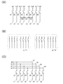
本実施の形態では、本発明の一態様の半導体装置について図1〜図7を参照して説明する。
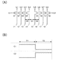
本実施の形態では、本発明の一態様の半導体装置について説明する。具体的には、データ分割駆動を行うアクティブマトリクス型の表示装置の一例について、図8〜図12を参照して説明する。
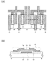
本実施の形態では、実施の形態1又は2に示した半導体装置が有するトランジスタの一例について説明する。具体的には、酸化物半導体によってチャネル形成領域が構成されるトランジスタの構造及び該トランジスタの作製方法の一例について、図13を参照して説明する。
本実施の形態では、実施の形態1又は2で得られる半導体装置を搭載した電子機器の例について図14を参照して説明する。
21〜28 スイッチ
31〜34 配線
41〜48 トランジスタ
50 基板
51 導電層
52 絶縁層
53 半導体層
54 導電層
55 導電層
61〜68 トランジスタ
70 基板
71 絶縁層
72 半導体層
73 絶縁層
74 導電層
75 絶縁層
76 導電層
77 導電層
101 画素部
102 ソース信号線駆動回路
103 ゲート信号線駆動回路
104 ソース信号線
105 ゲート信号線
106A フレキシブルプリント基板
106B フレキシブルプリント基板
107 画素
111 シフトレジスタ回路
112 サンプリング回路
121〜124 データ信号線
131〜139 トランジスタ
141〜149 ソース信号線
400 基板
402 ゲート絶縁層
403 保護絶縁層
410 トランジスタ
411 ゲート電極層
413 チャネル形成領域
414a ソース領域
414b ドレイン領域
415a ソース電極層
415b ドレイン電極層
416 酸化物絶縁層
430 酸化物半導体膜
431 酸化物半導体層
2201 本体
2202 筐体
2203 表示部
2204 キーボード
2211 本体
2212 スタイラス
2213 表示部
2214 操作ボタン
2215 外部インターフェイス
2220 電子書籍
2221 筐体
2223 筐体
2225 表示部
2227 表示部
2231 電源
2233 操作キー
2235 スピーカー
2237 軸部
2240 筐体
2241 筐体
2242 表示パネル
2243 スピーカー
2244 マイクロフォン
2245 操作キー
2246 ポインティングデバイス
2247 カメラ用レンズ
2248 外部接続端子
2249 太陽電池セル
2250 外部メモリスロット
2261 本体
2263 接眼部
2264 操作スイッチ
2265 表示部(B)
2266 バッテリー
2267 表示部(A)
2270 テレビジョン装置
2271 筐体
2273 表示部
2275 スタンド
2277 表示部
2279 操作キー
2280 リモコン操作機
Claims (14)
- 第1の期間においてオン状態となり、且つ第2の期間においてオフ状態となる第1のスイッチ乃至第nのスイッチ(nは2以上の自然数)と、
前記第1の期間においてオフ状態となり、且つ前記第2の期間においてオン状態となる第n+1のスイッチ乃至第mのスイッチ(mはn+2以上の自然数)と、
前記第1の期間において前記第1のスイッチを介して信号が供給され、且つ前記第2の期間において浮遊状態となる第1の信号線、乃至、前記第1の期間において前記第nのスイッチを介して信号が供給され、且つ前記第2の期間において浮遊状態となる第nの信号線と、
前記第1の期間において浮遊状態となり、且つ前記第2の期間において前記第n+1のスイッチを介して信号が供給される第n+1の信号線、乃至、前記第1の期間において浮遊状態となり、且つ前記第2の期間において前記第mのスイッチを介して信号が供給される第mの信号線と、を有し、
前記第1の信号線乃至前記第mの信号線は、各々が平行又は略平行に配列し、
前記第nの信号線と前記第n+1の信号線の間隔は、前記第n−1の信号線と前記第nの信号線の間隔よりも広く、且つ前記第n+1の信号線と前記第n+2の信号線の間隔よりも広いことを特徴とする半導体装置。 - 請求項1において、
前記第1の信号線乃至前記第nの信号線のいずれか一及び前記第n+1の信号線乃至前記第mの信号線のいずれか一に対する信号の供給が、同一の配線を介して行われることを特徴とする半導体装置。 - 請求項1又は請求項2において、
前記第1のスイッチ乃至前記第mのスイッチのそれぞれが、第1のトランジスタ乃至第mのトランジスタのそれぞれであることを特徴とする半導体装置。 - 請求項3において、
前記第1のトランジスタ乃至前記第mのトランジスタは、各々が等間隔又は略等間隔に配列し、且つ各々のチャネル長方向が、前記第1の信号線乃至前記第mの信号線に垂直又は略垂直に設けられ、
前記第nのトランジスタのソース端子及びドレイン端子の一方が他方よりも前記第n+1のトランジスタに近接し、
前記第n+1のトランジスタのソース端子及びドレイン端子の一方が他方よりも前記第nのトランジスタに近接し、
前記第nのトランジスタのソース端子及びドレイン端子の他方が、前記第nの信号線に電気的に接続され、
前記第n+1のトランジスタのソース端子及びドレイン端子の他方が、前記第n+1の信号線に電気的に接続されることを特徴とする半導体装置。 - 第1の期間においてオン状態となり、且つ第2の期間においてオフ状態となる第1のスイッチ乃至第nのスイッチ(nは2以上の自然数)と、
前記第1の期間においてオフ状態となり、且つ前記第2の期間においてオン状態となる第n+1のスイッチ乃至第mのスイッチ(mはn+2以上の自然数)と、
前記第1の期間において前記第1のスイッチを介して画像信号が供給され、且つ前記第2の期間において浮遊状態となる第1のソース信号線、乃至、前記第1の期間において前記第nのスイッチを介して画像信号が供給され、且つ前記第2の期間において浮遊状態となる第nのソース信号線と、
前記第1の期間において浮遊状態となり、且つ前記第2の期間において前記第n+1のスイッチを介して画像信号が供給される第n+1のソース信号線、乃至、前記第1の期間において浮遊状態となり、且つ前記第2の期間において前記第mのスイッチを介して画像信号が供給される第mのソース信号線と、を有し、
前記第1のソース信号線乃至前記第mのソース信号線は、各々が平行又は略平行に配列し、
前記第nのソース信号線と前記第n+1のソース信号線の間隔は、前記第n−1のソース信号線と前記第nのソース信号線の間隔よりも広く、且つ前記第n+1のソース信号線と前記第n+2のソース信号線の間隔よりも広いことを特徴とする半導体装置。 - 請求項5において、
前記第1のソース信号線乃至前記第nのソース信号線のいずれか一及び前記第n+1のソース信号線乃至前記第mのソース信号線のいずれか一に対する画像信号の供給が、同一のデータ信号線を介して行われることを特徴とする半導体装置。 - 請求項5又は請求項6において、
前記第1のスイッチ乃至前記第mのスイッチが、第1のトランジスタ乃至第mのトランジスタであることを特徴とする半導体装置。 - 請求項7において、
前記第1のトランジスタ乃至前記第mのトランジスタは、各々が等間隔又は略等間隔に配列し、且つ各々のチャネル長方向が、前記第1のソース信号線乃至前記第mのソース信号線に垂直又は略垂直に設けられ、
前記第nのトランジスタのソース端子及びドレイン端子の一方が他方よりも前記第n+1のトランジスタに近接し、
前記第n+1のトランジスタのソース端子及びドレイン端子の一方が他方よりも前記第nのトランジスタに近接し、
前記第nのトランジスタのソース端子及びドレイン端子の他方が、前記第nのソース信号線に電気的に接続され、
前記第n+1のトランジスタのソース端子及びドレイン端子の他方が、前記第n+1のソース信号線に電気的に接続されることを特徴とする半導体装置。 - 請求項7又は請求項8において、
前記第1のトランジスタ乃至前記第mのトランジスタのチャネル形成領域が、酸化物半導体によって構成されることを特徴とする半導体装置。 - 請求項9において、
前記第1のトランジスタ乃至前記第mのトランジスタのスイッチングを制御するシフトレジスタ回路を有し、
前記シフトレジスタ回路は、チャネル形成領域が酸化物半導体によって構成されるトランジスタを有することを特徴とする半導体装置。 - 請求項5乃至請求項10のいずれか一項において、
前記第1のソース信号線乃至前記第mのソース信号線のいずれか一に電気的に接続された画素を有し、
前記画素は、チャネル形成領域が酸化物半導体によって構成されるトランジスタを有することを特徴とする半導体装置。 - 請求項11において、
前記画素が有するトランジスタのスイッチングを制御するゲート信号線駆動回路を有し、
前記ゲート信号線駆動回路は、チャネル形成領域が酸化物半導体によって構成されるトランジスタを有することを特徴とする半導体装置。 - 請求項1乃至請求項12のいずれか一項において、
m=2nであることを特徴とする半導体装置。 - 請求項1乃至請求項13のいずれか一項に記載の半導体装置を有する電子機器。
Priority Applications (1)
| Application Number | Priority Date | Filing Date | Title |
|---|---|---|---|
| JP2011000549A JP2011164591A (ja) | 2010-01-15 | 2011-01-05 | 半導体装置及び電子機器 |
Applications Claiming Priority (3)
| Application Number | Priority Date | Filing Date | Title |
|---|---|---|---|
| JP2010006419 | 2010-01-15 | ||
| JP2010006419 | 2010-01-15 | ||
| JP2011000549A JP2011164591A (ja) | 2010-01-15 | 2011-01-05 | 半導体装置及び電子機器 |
Publications (2)
| Publication Number | Publication Date |
|---|---|
| JP2011164591A true JP2011164591A (ja) | 2011-08-25 |
| JP2011164591A5 JP2011164591A5 (ja) | 2014-02-13 |
Family
ID=44277193
Family Applications (1)
| Application Number | Title | Priority Date | Filing Date |
|---|---|---|---|
| JP2011000549A Withdrawn JP2011164591A (ja) | 2010-01-15 | 2011-01-05 | 半導体装置及び電子機器 |
Country Status (6)
| Country | Link |
|---|---|
| US (2) | US8796785B2 (ja) |
| JP (1) | JP2011164591A (ja) |
| KR (1) | KR101748763B1 (ja) |
| CN (1) | CN102696064B (ja) |
| TW (2) | TWI573111B (ja) |
| WO (1) | WO2011086837A1 (ja) |
Cited By (3)
| Publication number | Priority date | Publication date | Assignee | Title |
|---|---|---|---|---|
| JP2015087491A (ja) * | 2013-10-30 | 2015-05-07 | キヤノン株式会社 | 発光素子の駆動回路、露光ヘッド及び画像形成装置 |
| JP2015179259A (ja) * | 2014-02-27 | 2015-10-08 | 株式会社半導体エネルギー研究所 | 半導体装置、並びにそれを備えるモジュールおよび電子機器 |
| JP2017152735A (ja) * | 2011-08-31 | 2017-08-31 | 株式会社半導体エネルギー研究所 | 表示装置 |
Families Citing this family (3)
| Publication number | Priority date | Publication date | Assignee | Title |
|---|---|---|---|---|
| JPWO2016152492A1 (ja) | 2015-03-26 | 2017-12-28 | 富士フイルム株式会社 | マトリクス装置およびマトリクス装置の製造方法 |
| TWI750448B (zh) * | 2019-01-28 | 2021-12-21 | 友達光電股份有限公司 | 觸控顯示裝置 |
| JP2022127330A (ja) * | 2021-02-19 | 2022-08-31 | キオクシア株式会社 | 半導体集積回路 |
Citations (2)
| Publication number | Priority date | Publication date | Assignee | Title |
|---|---|---|---|---|
| JP2000148067A (ja) * | 1998-11-12 | 2000-05-26 | Sharp Corp | データ信号線駆動回路および画像表示装置 |
| JP2005077483A (ja) * | 2003-08-28 | 2005-03-24 | Seiko Epson Corp | 電気光学装置及び電子機器 |
Family Cites Families (119)
| Publication number | Priority date | Publication date | Assignee | Title |
|---|---|---|---|---|
| JPS60198861A (ja) | 1984-03-23 | 1985-10-08 | Fujitsu Ltd | 薄膜トランジスタ |
| JPH0244256B2 (ja) | 1987-01-28 | 1990-10-03 | Kagaku Gijutsucho Mukizaishitsu Kenkyushocho | Ingazn2o5deshimesarerurotsuhoshokeinosojokozoojusurukagobutsuoyobisonoseizoho |
| JPS63210023A (ja) | 1987-02-24 | 1988-08-31 | Natl Inst For Res In Inorg Mater | InGaZn↓4O↓7で示される六方晶系の層状構造を有する化合物およびその製造法 |
| JPH0244258B2 (ja) | 1987-02-24 | 1990-10-03 | Kagaku Gijutsucho Mukizaishitsu Kenkyushocho | Ingazn3o6deshimesarerurotsuhoshokeinosojokozoojusurukagobutsuoyobisonoseizoho |
| JPH0244260B2 (ja) | 1987-02-24 | 1990-10-03 | Kagaku Gijutsucho Mukizaishitsu Kenkyushocho | Ingazn5o8deshimesarerurotsuhoshokeinosojokozoojusurukagobutsuoyobisonoseizoho |
| JPH0244262B2 (ja) | 1987-02-27 | 1990-10-03 | Kagaku Gijutsucho Mukizaishitsu Kenkyushocho | Ingazn6o9deshimesarerurotsuhoshokeinosojokozoojusurukagobutsuoyobisonoseizoho |
| JPH0244263B2 (ja) | 1987-04-22 | 1990-10-03 | Kagaku Gijutsucho Mukizaishitsu Kenkyushocho | Ingazn7o10deshimesarerurotsuhoshokeinosojokozoojusurukagobutsuoyobisonoseizoho |
| JP2653099B2 (ja) * | 1988-05-17 | 1997-09-10 | セイコーエプソン株式会社 | アクティブマトリクスパネル,投写型表示装置及びビューファインダー |
| JPH05251705A (ja) | 1992-03-04 | 1993-09-28 | Fuji Xerox Co Ltd | 薄膜トランジスタ |
| JP3476885B2 (ja) | 1992-12-24 | 2003-12-10 | 株式会社東芝 | 表示装置 |
| JP3050738B2 (ja) | 1993-12-17 | 2000-06-12 | シャープ株式会社 | 表示装置の駆動回路 |
| US5555001A (en) * | 1994-03-08 | 1996-09-10 | Prime View Hk Limited | Redundant scheme for LCD display with integrated data driving circuit |
| JPH0850465A (ja) * | 1994-05-30 | 1996-02-20 | Sanyo Electric Co Ltd | シフトレジスタ及び表示装置の駆動回路 |
| JP3479375B2 (ja) | 1995-03-27 | 2003-12-15 | 科学技術振興事業団 | 亜酸化銅等の金属酸化物半導体による薄膜トランジスタとpn接合を形成した金属酸化物半導体装置およびそれらの製造方法 |
| EP0820644B1 (en) * | 1995-08-03 | 2005-08-24 | Koninklijke Philips Electronics N.V. | Semiconductor device provided with transparent switching element |
| JP3625598B2 (ja) * | 1995-12-30 | 2005-03-02 | 三星電子株式会社 | 液晶表示装置の製造方法 |
| JP3727416B2 (ja) | 1996-05-31 | 2005-12-14 | 株式会社半導体エネルギー研究所 | 表示装置 |
| KR100338007B1 (ko) * | 1997-09-30 | 2002-10-11 | 삼성전자 주식회사 | 액정 표시 장치 및 그의 구동 방법 |
| JP4170454B2 (ja) | 1998-07-24 | 2008-10-22 | Hoya株式会社 | 透明導電性酸化物薄膜を有する物品及びその製造方法 |
| JP2000150861A (ja) * | 1998-11-16 | 2000-05-30 | Tdk Corp | 酸化物薄膜 |
| JP3276930B2 (ja) | 1998-11-17 | 2002-04-22 | 科学技術振興事業団 | トランジスタ及び半導体装置 |
| TW460731B (en) * | 1999-09-03 | 2001-10-21 | Ind Tech Res Inst | Electrode structure and production method of wide viewing angle LCD |
| JP4089858B2 (ja) | 2000-09-01 | 2008-05-28 | 国立大学法人東北大学 | 半導体デバイス |
| KR20020038482A (ko) * | 2000-11-15 | 2002-05-23 | 모리시타 요이찌 | 박막 트랜지스터 어레이, 그 제조방법 및 그것을 이용한표시패널 |
| JP3997731B2 (ja) * | 2001-03-19 | 2007-10-24 | 富士ゼロックス株式会社 | 基材上に結晶性半導体薄膜を形成する方法 |
| JP2002289859A (ja) | 2001-03-23 | 2002-10-04 | Minolta Co Ltd | 薄膜トランジスタ |
| JP2003022054A (ja) * | 2001-07-06 | 2003-01-24 | Sharp Corp | 画像表示装置 |
| JP4090716B2 (ja) * | 2001-09-10 | 2008-05-28 | 雅司 川崎 | 薄膜トランジスタおよびマトリクス表示装置 |
| JP3925839B2 (ja) | 2001-09-10 | 2007-06-06 | シャープ株式会社 | 半導体記憶装置およびその試験方法 |
| KR100825093B1 (ko) * | 2001-09-27 | 2008-04-25 | 삼성전자주식회사 | 액정 표시 장치 |
| JP4164562B2 (ja) | 2002-09-11 | 2008-10-15 | 独立行政法人科学技術振興機構 | ホモロガス薄膜を活性層として用いる透明薄膜電界効果型トランジスタ |
| WO2003040441A1 (en) * | 2001-11-05 | 2003-05-15 | Japan Science And Technology Agency | Natural superlattice homologous single crystal thin film, method for preparation thereof, and device using said single crystal thin film |
| JP4083486B2 (ja) * | 2002-02-21 | 2008-04-30 | 独立行政法人科学技術振興機構 | LnCuO(S,Se,Te)単結晶薄膜の製造方法 |
| US7049190B2 (en) * | 2002-03-15 | 2006-05-23 | Sanyo Electric Co., Ltd. | Method for forming ZnO film, method for forming ZnO semiconductor layer, method for fabricating semiconductor device, and semiconductor device |
| JP3933591B2 (ja) * | 2002-03-26 | 2007-06-20 | 淳二 城戸 | 有機エレクトロルミネッセント素子 |
| US7339187B2 (en) * | 2002-05-21 | 2008-03-04 | State Of Oregon Acting By And Through The Oregon State Board Of Higher Education On Behalf Of Oregon State University | Transistor structures |
| JP2004022625A (ja) * | 2002-06-13 | 2004-01-22 | Murata Mfg Co Ltd | 半導体デバイス及び該半導体デバイスの製造方法 |
| US7105868B2 (en) * | 2002-06-24 | 2006-09-12 | Cermet, Inc. | High-electron mobility transistor with zinc oxide |
| US7067843B2 (en) * | 2002-10-11 | 2006-06-27 | E. I. Du Pont De Nemours And Company | Transparent oxide semiconductor thin film transistors |
| US7327168B2 (en) * | 2002-11-20 | 2008-02-05 | Semiconductor Energy Laboratory Co., Ltd. | Semiconductor device and driving method thereof |
| JP4166105B2 (ja) | 2003-03-06 | 2008-10-15 | シャープ株式会社 | 半導体装置およびその製造方法 |
| JP2004273732A (ja) | 2003-03-07 | 2004-09-30 | Sharp Corp | アクティブマトリクス基板およびその製造方法 |
| JP4108633B2 (ja) | 2003-06-20 | 2008-06-25 | シャープ株式会社 | 薄膜トランジスタおよびその製造方法ならびに電子デバイス |
| US7262463B2 (en) * | 2003-07-25 | 2007-08-28 | Hewlett-Packard Development Company, L.P. | Transistor including a deposited channel region having a doped portion |
| JP4029802B2 (ja) | 2003-08-28 | 2008-01-09 | セイコーエプソン株式会社 | 電気光学装置の駆動回路、電気光学装置及び電子機器 |
| US7282782B2 (en) * | 2004-03-12 | 2007-10-16 | Hewlett-Packard Development Company, L.P. | Combined binary oxide semiconductor device |
| US7297977B2 (en) * | 2004-03-12 | 2007-11-20 | Hewlett-Packard Development Company, L.P. | Semiconductor device |
| US7145174B2 (en) * | 2004-03-12 | 2006-12-05 | Hewlett-Packard Development Company, Lp. | Semiconductor device |
| KR101078483B1 (ko) | 2004-03-12 | 2011-10-31 | 도꾸리쯔교세이호징 가가꾸 기쥬쯔 신꼬 기꼬 | Lcd 또는 유기 el 디스플레이의 스위칭 소자 |
| US7211825B2 (en) * | 2004-06-14 | 2007-05-01 | Yi-Chi Shih | Indium oxide-based thin film transistors and circuits |
| JP2006100760A (ja) * | 2004-09-02 | 2006-04-13 | Casio Comput Co Ltd | 薄膜トランジスタおよびその製造方法 |
| US7285501B2 (en) * | 2004-09-17 | 2007-10-23 | Hewlett-Packard Development Company, L.P. | Method of forming a solution processed device |
| US7298084B2 (en) * | 2004-11-02 | 2007-11-20 | 3M Innovative Properties Company | Methods and displays utilizing integrated zinc oxide row and column drivers in conjunction with organic light emitting diodes |
| US7868326B2 (en) * | 2004-11-10 | 2011-01-11 | Canon Kabushiki Kaisha | Field effect transistor |
| US7863611B2 (en) * | 2004-11-10 | 2011-01-04 | Canon Kabushiki Kaisha | Integrated circuits utilizing amorphous oxides |
| EP2455975B1 (en) * | 2004-11-10 | 2015-10-28 | Canon Kabushiki Kaisha | Field effect transistor with amorphous oxide |
| US7791072B2 (en) * | 2004-11-10 | 2010-09-07 | Canon Kabushiki Kaisha | Display |
| US7829444B2 (en) * | 2004-11-10 | 2010-11-09 | Canon Kabushiki Kaisha | Field effect transistor manufacturing method |
| EP1810335B1 (en) * | 2004-11-10 | 2020-05-27 | Canon Kabushiki Kaisha | Light-emitting device |
| US7453065B2 (en) * | 2004-11-10 | 2008-11-18 | Canon Kabushiki Kaisha | Sensor and image pickup device |
| US7671833B2 (en) * | 2004-11-22 | 2010-03-02 | Samsung Electronics Co., Ltd. | Touch sensible display device |
| US7579224B2 (en) * | 2005-01-21 | 2009-08-25 | Semiconductor Energy Laboratory Co., Ltd. | Method for manufacturing a thin film semiconductor device |
| TWI412138B (zh) * | 2005-01-28 | 2013-10-11 | Semiconductor Energy Lab | 半導體裝置,電子裝置,和半導體裝置的製造方法 |
| TWI445178B (zh) * | 2005-01-28 | 2014-07-11 | Semiconductor Energy Lab | 半導體裝置,電子裝置,和半導體裝置的製造方法 |
| US7858451B2 (en) * | 2005-02-03 | 2010-12-28 | Semiconductor Energy Laboratory Co., Ltd. | Electronic device, semiconductor device and manufacturing method thereof |
| US7948171B2 (en) * | 2005-02-18 | 2011-05-24 | Semiconductor Energy Laboratory Co., Ltd. | Light emitting device |
| US20060197092A1 (en) * | 2005-03-03 | 2006-09-07 | Randy Hoffman | System and method for forming conductive material on a substrate |
| US8681077B2 (en) | 2005-03-18 | 2014-03-25 | Semiconductor Energy Laboratory Co., Ltd. | Semiconductor device, and display device, driving method and electronic apparatus thereof |
| WO2006105077A2 (en) * | 2005-03-28 | 2006-10-05 | Massachusetts Institute Of Technology | Low voltage thin film transistor with high-k dielectric material |
| US7645478B2 (en) * | 2005-03-31 | 2010-01-12 | 3M Innovative Properties Company | Methods of making displays |
| US8300031B2 (en) * | 2005-04-20 | 2012-10-30 | Semiconductor Energy Laboratory Co., Ltd. | Semiconductor device comprising transistor having gate and drain connected through a current-voltage conversion element |
| JP2006344849A (ja) * | 2005-06-10 | 2006-12-21 | Casio Comput Co Ltd | 薄膜トランジスタ |
| US7691666B2 (en) * | 2005-06-16 | 2010-04-06 | Eastman Kodak Company | Methods of making thin film transistors comprising zinc-oxide-based semiconductor materials and transistors made thereby |
| US7402506B2 (en) * | 2005-06-16 | 2008-07-22 | Eastman Kodak Company | Methods of making thin film transistors comprising zinc-oxide-based semiconductor materials and transistors made thereby |
| US7507618B2 (en) | 2005-06-27 | 2009-03-24 | 3M Innovative Properties Company | Method for making electronic devices using metal oxide nanoparticles |
| KR100711890B1 (ko) * | 2005-07-28 | 2007-04-25 | 삼성에스디아이 주식회사 | 유기 발광표시장치 및 그의 제조방법 |
| JP2007059128A (ja) * | 2005-08-23 | 2007-03-08 | Canon Inc | 有機el表示装置およびその製造方法 |
| JP5116225B2 (ja) * | 2005-09-06 | 2013-01-09 | キヤノン株式会社 | 酸化物半導体デバイスの製造方法 |
| JP2007073705A (ja) * | 2005-09-06 | 2007-03-22 | Canon Inc | 酸化物半導体チャネル薄膜トランジスタおよびその製造方法 |
| JP4280736B2 (ja) * | 2005-09-06 | 2009-06-17 | キヤノン株式会社 | 半導体素子 |
| JP4850457B2 (ja) * | 2005-09-06 | 2012-01-11 | キヤノン株式会社 | 薄膜トランジスタ及び薄膜ダイオード |
| FR2890759B1 (fr) * | 2005-09-09 | 2007-11-02 | Thales Sa | Afficheur matriciel a cristaux liquides du type a matrice active |
| EP3614442A3 (en) * | 2005-09-29 | 2020-03-25 | Semiconductor Energy Laboratory Co., Ltd. | Semiconductor device having oxide semiconductor layer and manufactoring method thereof |
| US7310402B2 (en) | 2005-10-18 | 2007-12-18 | Au Optronics Corporation | Gate line drivers for active matrix displays |
| JP5037808B2 (ja) * | 2005-10-20 | 2012-10-03 | キヤノン株式会社 | アモルファス酸化物を用いた電界効果型トランジスタ、及び該トランジスタを用いた表示装置 |
| CN101707212B (zh) * | 2005-11-15 | 2012-07-11 | 株式会社半导体能源研究所 | 半导体器件及其制造方法 |
| TWI292281B (en) * | 2005-12-29 | 2008-01-01 | Ind Tech Res Inst | Pixel structure of active organic light emitting diode and method of fabricating the same |
| US7867636B2 (en) * | 2006-01-11 | 2011-01-11 | Murata Manufacturing Co., Ltd. | Transparent conductive film and method for manufacturing the same |
| JP4977478B2 (ja) * | 2006-01-21 | 2012-07-18 | 三星電子株式会社 | ZnOフィルム及びこれを用いたTFTの製造方法 |
| US7576394B2 (en) * | 2006-02-02 | 2009-08-18 | Kochi Industrial Promotion Center | Thin film transistor including low resistance conductive thin films and manufacturing method thereof |
| US7977169B2 (en) * | 2006-02-15 | 2011-07-12 | Kochi Industrial Promotion Center | Semiconductor device including active layer made of zinc oxide with controlled orientations and manufacturing method thereof |
| KR20070101595A (ko) * | 2006-04-11 | 2007-10-17 | 삼성전자주식회사 | ZnO TFT |
| US20070252928A1 (en) * | 2006-04-28 | 2007-11-01 | Toppan Printing Co., Ltd. | Structure, transmission type liquid crystal display, reflection type display and manufacturing method thereof |
| JP5028033B2 (ja) | 2006-06-13 | 2012-09-19 | キヤノン株式会社 | 酸化物半導体膜のドライエッチング方法 |
| JP4999400B2 (ja) * | 2006-08-09 | 2012-08-15 | キヤノン株式会社 | 酸化物半導体膜のドライエッチング方法 |
| JP4609797B2 (ja) * | 2006-08-09 | 2011-01-12 | Nec液晶テクノロジー株式会社 | 薄膜デバイス及びその製造方法 |
| JP4332545B2 (ja) * | 2006-09-15 | 2009-09-16 | キヤノン株式会社 | 電界効果型トランジスタ及びその製造方法 |
| JP5164357B2 (ja) * | 2006-09-27 | 2013-03-21 | キヤノン株式会社 | 半導体装置及び半導体装置の製造方法 |
| JP4274219B2 (ja) * | 2006-09-27 | 2009-06-03 | セイコーエプソン株式会社 | 電子デバイス、有機エレクトロルミネッセンス装置、有機薄膜半導体装置 |
| US7622371B2 (en) * | 2006-10-10 | 2009-11-24 | Hewlett-Packard Development Company, L.P. | Fused nanocrystal thin film semiconductor and method |
| US7772021B2 (en) * | 2006-11-29 | 2010-08-10 | Samsung Electronics Co., Ltd. | Flat panel displays comprising a thin-film transistor having a semiconductive oxide in its channel and methods of fabricating the same for use in flat panel displays |
| JP2008140684A (ja) * | 2006-12-04 | 2008-06-19 | Toppan Printing Co Ltd | カラーelディスプレイおよびその製造方法 |
| TWI341507B (en) * | 2006-12-29 | 2011-05-01 | Chimei Innolux Corp | Shift register and liquid crystal display device |
| KR101303578B1 (ko) * | 2007-01-05 | 2013-09-09 | 삼성전자주식회사 | 박막 식각 방법 |
| US8207063B2 (en) * | 2007-01-26 | 2012-06-26 | Eastman Kodak Company | Process for atomic layer deposition |
| KR100851215B1 (ko) * | 2007-03-14 | 2008-08-07 | 삼성에스디아이 주식회사 | 박막 트랜지스터 및 이를 이용한 유기 전계 발광표시장치 |
| US7795613B2 (en) * | 2007-04-17 | 2010-09-14 | Toppan Printing Co., Ltd. | Structure with transistor |
| KR101325053B1 (ko) * | 2007-04-18 | 2013-11-05 | 삼성디스플레이 주식회사 | 박막 트랜지스터 기판 및 이의 제조 방법 |
| KR20080094300A (ko) * | 2007-04-19 | 2008-10-23 | 삼성전자주식회사 | 박막 트랜지스터 및 그 제조 방법과 박막 트랜지스터를포함하는 평판 디스플레이 |
| KR101334181B1 (ko) * | 2007-04-20 | 2013-11-28 | 삼성전자주식회사 | 선택적으로 결정화된 채널층을 갖는 박막 트랜지스터 및 그제조 방법 |
| CN101663762B (zh) * | 2007-04-25 | 2011-09-21 | 佳能株式会社 | 氧氮化物半导体 |
| KR101345376B1 (ko) | 2007-05-29 | 2013-12-24 | 삼성전자주식회사 | ZnO 계 박막 트랜지스터 및 그 제조방법 |
| DE102007040712B4 (de) * | 2007-08-23 | 2014-09-04 | Seereal Technologies S.A. | Elektronisches Anzeigegerät und Vorrichtung zur Ansteuerung von Pixeln eines Displays |
| US8349662B2 (en) * | 2007-12-11 | 2013-01-08 | Micron Technology, Inc. | Integrated circuit having memory cell array, and method of manufacturing same |
| JP5215158B2 (ja) * | 2007-12-17 | 2013-06-19 | 富士フイルム株式会社 | 無機結晶性配向膜及びその製造方法、半導体デバイス |
| WO2009093625A1 (ja) * | 2008-01-23 | 2009-07-30 | Idemitsu Kosan Co., Ltd. | 電界効果型トランジスタ及びその製造方法、それを用いた表示装置、並びに半導体装置 |
| KR101484291B1 (ko) * | 2008-06-17 | 2015-01-20 | 삼성디스플레이 주식회사 | 데이터 드라이버 및 이를 갖는 표시장치 |
| JP4623179B2 (ja) * | 2008-09-18 | 2011-02-02 | ソニー株式会社 | 薄膜トランジスタおよびその製造方法 |
| JP5451280B2 (ja) * | 2008-10-09 | 2014-03-26 | キヤノン株式会社 | ウルツ鉱型結晶成長用基板およびその製造方法ならびに半導体装置 |
-
2010
- 2010-12-17 KR KR1020127021384A patent/KR101748763B1/ko active IP Right Grant
- 2010-12-17 WO PCT/JP2010/073476 patent/WO2011086837A1/en active Application Filing
- 2010-12-17 CN CN201080061403.7A patent/CN102696064B/zh not_active Expired - Fee Related
-
2011
- 2011-01-05 JP JP2011000549A patent/JP2011164591A/ja not_active Withdrawn
- 2011-01-05 TW TW104130437A patent/TWI573111B/zh active
- 2011-01-05 TW TW100100330A patent/TWI511109B/zh active
- 2011-01-12 US US13/005,232 patent/US8796785B2/en active Active
-
2014
- 2014-07-31 US US14/448,180 patent/US9484365B2/en active Active
Patent Citations (2)
| Publication number | Priority date | Publication date | Assignee | Title |
|---|---|---|---|---|
| JP2000148067A (ja) * | 1998-11-12 | 2000-05-26 | Sharp Corp | データ信号線駆動回路および画像表示装置 |
| JP2005077483A (ja) * | 2003-08-28 | 2005-03-24 | Seiko Epson Corp | 電気光学装置及び電子機器 |
Cited By (6)
| Publication number | Priority date | Publication date | Assignee | Title |
|---|---|---|---|---|
| JP2017152735A (ja) * | 2011-08-31 | 2017-08-31 | 株式会社半導体エネルギー研究所 | 表示装置 |
| JP2015087491A (ja) * | 2013-10-30 | 2015-05-07 | キヤノン株式会社 | 発光素子の駆動回路、露光ヘッド及び画像形成装置 |
| JP2015179259A (ja) * | 2014-02-27 | 2015-10-08 | 株式会社半導体エネルギー研究所 | 半導体装置、並びにそれを備えるモジュールおよび電子機器 |
| US10483293B2 (en) | 2014-02-27 | 2019-11-19 | Semiconductor Energy Laboratory Co., Ltd. | Active matrix display device, and module and electronic appliance including the same |
| US11605655B2 (en) | 2014-02-27 | 2023-03-14 | Semiconductor Energy Laboratory Co., Ltd. | Semiconductor device, and module and electronic appliance including the same |
| US11916088B2 (en) | 2014-02-27 | 2024-02-27 | Semiconductor Energy Laboratory Co., Ltd. | Semiconductor device, and module and electronic appliance including the same |
Also Published As
| Publication number | Publication date |
|---|---|
| WO2011086837A1 (en) | 2011-07-21 |
| CN102696064A (zh) | 2012-09-26 |
| KR101748763B1 (ko) | 2017-06-20 |
| TWI573111B (zh) | 2017-03-01 |
| US20140339553A1 (en) | 2014-11-20 |
| US8796785B2 (en) | 2014-08-05 |
| TW201145244A (en) | 2011-12-16 |
| TWI511109B (zh) | 2015-12-01 |
| KR20120127451A (ko) | 2012-11-21 |
| US20110175670A1 (en) | 2011-07-21 |
| CN102696064B (zh) | 2015-11-25 |
| TW201546789A (zh) | 2015-12-16 |
| US9484365B2 (en) | 2016-11-01 |
Similar Documents
| Publication | Publication Date | Title |
|---|---|---|
| JP6810197B2 (ja) | 液晶表示装置 | |
| JP6321259B2 (ja) | 半導体装置 | |
| US11790866B1 (en) | Display device | |
| JP5713729B2 (ja) | 表示装置 | |
| US9484365B2 (en) | Semiconductor device including switch electrically connected to signal line | |
| JP5960779B2 (ja) | 液晶表示装置 | |
| JP2011186451A (ja) | 表示装置 |
Legal Events
| Date | Code | Title | Description |
|---|---|---|---|
| A521 | Request for written amendment filed |
Free format text: JAPANESE INTERMEDIATE CODE: A523 Effective date: 20131220 |
|
| A621 | Written request for application examination |
Free format text: JAPANESE INTERMEDIATE CODE: A621 Effective date: 20131220 |
|
| A977 | Report on retrieval |
Free format text: JAPANESE INTERMEDIATE CODE: A971007 Effective date: 20140922 |
|
| A131 | Notification of reasons for refusal |
Free format text: JAPANESE INTERMEDIATE CODE: A131 Effective date: 20140930 |
|
| A521 | Request for written amendment filed |
Free format text: JAPANESE INTERMEDIATE CODE: A523 Effective date: 20141113 |
|
| A02 | Decision of refusal |
Free format text: JAPANESE INTERMEDIATE CODE: A02 Effective date: 20150512 |
|
| A761 | Written withdrawal of application |
Free format text: JAPANESE INTERMEDIATE CODE: A761 Effective date: 20150622 |