JP2010244596A - 集積回路 - Google Patents
集積回路 Download PDFInfo
- Publication number
- JP2010244596A JP2010244596A JP2009089878A JP2009089878A JP2010244596A JP 2010244596 A JP2010244596 A JP 2010244596A JP 2009089878 A JP2009089878 A JP 2009089878A JP 2009089878 A JP2009089878 A JP 2009089878A JP 2010244596 A JP2010244596 A JP 2010244596A
- Authority
- JP
- Japan
- Prior art keywords
- fuse
- information
- circuit
- data
- redundancy
- Prior art date
- Legal status (The legal status is an assumption and is not a legal conclusion. Google has not performed a legal analysis and makes no representation as to the accuracy of the status listed.)
- Pending
Links
- 230000008439 repair process Effects 0.000 claims abstract description 214
- 230000002950 deficient Effects 0.000 claims abstract description 110
- 238000006243 chemical reaction Methods 0.000 claims abstract description 60
- 238000012360 testing method Methods 0.000 claims abstract description 59
- 230000006870 function Effects 0.000 claims abstract description 16
- 230000008859 change Effects 0.000 claims abstract description 6
- 238000001514 detection method Methods 0.000 abstract 1
- 230000007547 defect Effects 0.000 description 79
- 101100004188 Arabidopsis thaliana BARD1 gene Proteins 0.000 description 11
- 238000000034 method Methods 0.000 description 11
- 238000012545 processing Methods 0.000 description 10
- 238000013500 data storage Methods 0.000 description 8
- 239000004065 semiconductor Substances 0.000 description 7
- 238000004364 calculation method Methods 0.000 description 6
- 230000008569 process Effects 0.000 description 4
- 241000951471 Citrus junos Species 0.000 description 1
- 230000008901 benefit Effects 0.000 description 1
- 238000007664 blowing Methods 0.000 description 1
- 238000007796 conventional method Methods 0.000 description 1
- 230000000694 effects Effects 0.000 description 1
- 238000007689 inspection Methods 0.000 description 1
- 230000000717 retained effect Effects 0.000 description 1
- 238000004904 shortening Methods 0.000 description 1
- 238000012546 transfer Methods 0.000 description 1
Images


Classifications
-
- G—PHYSICS
- G11—INFORMATION STORAGE
- G11C—STATIC STORES
- G11C17/00—Read-only memories programmable only once; Semi-permanent stores, e.g. manually-replaceable information cards
- G11C17/14—Read-only memories programmable only once; Semi-permanent stores, e.g. manually-replaceable information cards in which contents are determined by selectively establishing, breaking or modifying connecting links by permanently altering the state of coupling elements, e.g. PROM
- G11C17/18—Auxiliary circuits, e.g. for writing into memory
-
- G—PHYSICS
- G11—INFORMATION STORAGE
- G11C—STATIC STORES
- G11C17/00—Read-only memories programmable only once; Semi-permanent stores, e.g. manually-replaceable information cards
- G11C17/14—Read-only memories programmable only once; Semi-permanent stores, e.g. manually-replaceable information cards in which contents are determined by selectively establishing, breaking or modifying connecting links by permanently altering the state of coupling elements, e.g. PROM
- G11C17/16—Read-only memories programmable only once; Semi-permanent stores, e.g. manually-replaceable information cards in which contents are determined by selectively establishing, breaking or modifying connecting links by permanently altering the state of coupling elements, e.g. PROM using electrically-fusible links
- G11C17/165—Memory cells which are electrically programmed to cause a change in resistance, e.g. to permit multiple resistance steps to be programmed rather than conduct to or from non-conduct change of fuses and antifuses
-
- G—PHYSICS
- G11—INFORMATION STORAGE
- G11C—STATIC STORES
- G11C29/00—Checking stores for correct operation ; Subsequent repair; Testing stores during standby or offline operation
- G11C29/04—Detection or location of defective memory elements, e.g. cell constructio details, timing of test signals
- G11C29/08—Functional testing, e.g. testing during refresh, power-on self testing [POST] or distributed testing
- G11C29/12—Built-in arrangements for testing, e.g. built-in self testing [BIST] or interconnection details
- G11C29/44—Indication or identification of errors, e.g. for repair
- G11C29/4401—Indication or identification of errors, e.g. for repair for self repair
-
- G—PHYSICS
- G11—INFORMATION STORAGE
- G11C—STATIC STORES
- G11C29/00—Checking stores for correct operation ; Subsequent repair; Testing stores during standby or offline operation
- G11C29/70—Masking faults in memories by using spares or by reconfiguring
- G11C29/78—Masking faults in memories by using spares or by reconfiguring using programmable devices
- G11C29/785—Masking faults in memories by using spares or by reconfiguring using programmable devices with redundancy programming schemes
-
- G—PHYSICS
- G11—INFORMATION STORAGE
- G11C—STATIC STORES
- G11C29/00—Checking stores for correct operation ; Subsequent repair; Testing stores during standby or offline operation
- G11C29/04—Detection or location of defective memory elements, e.g. cell constructio details, timing of test signals
- G11C29/08—Functional testing, e.g. testing during refresh, power-on self testing [POST] or distributed testing
- G11C29/12—Built-in arrangements for testing, e.g. built-in self testing [BIST] or interconnection details
- G11C2029/4402—Internal storage of test result, quality data, chip identification, repair information
Abstract
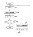
【解決手段】本発明は、複数のメモリセルと、複数のヒューズと、複数のヒューズのうち対応するヒューズが第1の状態となることで複数のメモリセルにある不良セルを救済する機能を有する冗長メモリと、既に救済され第1の不良セルに対応した第1の状態となっているヒューズの位置情報から第1の不良セルの第1の情報を生成するヒューズデータ変換回路と、複数のメモリセルのテスト結果により第2の不良セルを検出すると、第2の不良セルの第2の情報と第1の情報とに応じて、第2の不良セルを救済するための救済情報を生成する救済データ生成回路と、救済演算回路が生成した救済情報に応じて、複数のヒューズのうち、所定のヒューズを第1の状態とするヒューズ状態変更回路と、を有する集積回路である。
【選択図】図1
Description
110 BIST回路
120 リダンダンシ救済データ生成回路
121 不良情報記憶部
122 リダンダンシ救済データ設定部
123 リダンダンシ救済データ保持部
130、330 ヒューズデータ変換回路
140 ヒューズカット回路
150 ヒューズ部
160 ヒューズデータ読み出し回路
170、370 リダンダンシ救済演算データ変換回路
210 BIST部
220 BIST機能付リダンダンシ救済データ生成回路
331 IOアドレス変換回路
332 ヒューズビット変換回路
371 IOビット変換回路
372 リダンダンシ救済アドレス変換回路
Claims (7)
- 複数のメモリセルと、
複数のヒューズと、
前記複数のヒューズのうち、対応するヒューズが第1の状態となることで、前記複数のメモリセルにある不良セルを救済する機能を有する冗長メモリと、を有する集積回路であって、
既に救済され、第1の不良セルに対応した前記第1の状態となっているヒューズの位置情報から、前記第1の不良セルの第1の情報を生成するヒューズデータ変換回路と、
前記複数のメモリセルのテスト結果により第2の不良セルを検出すると、その検出した第2の不良セルの第2の情報と、前記第1の不良セルの第1の情報とに応じて、前記第2の不良セルを救済するための救済情報を生成する救済データ生成回路と、
前記救済データ生成回路が生成した救済情報に応じて、前記複数のヒューズのうち、所定のヒューズを第1の状態とするヒューズ状態変更回路と、
を有する集積回路。 - 前記救済データ生成回路は、
前記ヒューズデータ変換回路からの前記第1の不良セルの第1の情報を保持する保持部と、
前記複数のメモリセルのテスト結果である前記第2の不良セルの第2の情報と、前記保持部が保持する前記第1の不良セルの第1の情報とのデータ値が異なる場合、前記第2の不良セルの第2の情報に応じた救済情報を設定する救済データ設定部と、を有する
請求項1に記載の集積回路。 - 前記救済データ生成回路は、
前記複数のメモリセルのテストを行うテスト部を更に有する
請求項2に記載の集積回路。 - 前記複数のメモリセルのテストを行うテスト回路を更に有し、
前記救済データ生成回路は、
前記テスト回路のテスト結果である前記第2の不良セルの第2の情報を記憶する記憶部と、
前記ヒューズデータ変換回路からの前記第1の不良セルの第1の情報を保持する保持部と、
前記記憶部が記憶する前記第2の不良セルの第2の情報と、前記保持部が保持する前記第1の不良セルの第1の情報とのデータ値が異なる場合、前記第2の不良セルの第2の情報に応じた救済情報を設定する救済データ設定部と、を有する
請求項1に記載の集積回路。 - 前記第1の状態とは、ヒューズがカットされた状態である
請求項1〜請求項4のいずれか1項に記載の集積回路。 - ヒューズデータ変換回路は、
前記第1の不良セルに対応してカットされたヒューズの位置情報を読み出すヒューズデータ読み出し回路と、
前記ヒューズデータ読み出し回路が読み出したカットされたヒューズの位置情報から、前記第1の不良セルの第1の情報に変換する救済データ変換回路と、を有する
請求項5に記載の集積回路。 - ヒューズ状態変更回路は、
前記救済データ生成回路からの前記救済情報に応じて、カットするヒューズの位置情報を生成するヒューズデータ変換回路と、
前記ヒューズデータ変換回路からのヒューズの位置情報に応じたヒューズをカットするヒューズカット回路と、を有する
請求項5に記載の集積回路。
Priority Applications (2)
| Application Number | Priority Date | Filing Date | Title |
|---|---|---|---|
| JP2009089878A JP2010244596A (ja) | 2009-04-02 | 2009-04-02 | 集積回路 |
| US12/662,040 US8238177B2 (en) | 2009-04-02 | 2010-03-29 | Integrated circuit |
Applications Claiming Priority (1)
| Application Number | Priority Date | Filing Date | Title |
|---|---|---|---|
| JP2009089878A JP2010244596A (ja) | 2009-04-02 | 2009-04-02 | 集積回路 |
Publications (2)
| Publication Number | Publication Date |
|---|---|
| JP2010244596A true JP2010244596A (ja) | 2010-10-28 |
| JP2010244596A5 JP2010244596A5 (ja) | 2012-04-05 |
Family
ID=42826081
Family Applications (1)
| Application Number | Title | Priority Date | Filing Date |
|---|---|---|---|
| JP2009089878A Pending JP2010244596A (ja) | 2009-04-02 | 2009-04-02 | 集積回路 |
Country Status (2)
| Country | Link |
|---|---|
| US (1) | US8238177B2 (ja) |
| JP (1) | JP2010244596A (ja) |
Families Citing this family (9)
| Publication number | Priority date | Publication date | Assignee | Title |
|---|---|---|---|---|
| JP5664204B2 (ja) * | 2010-12-15 | 2015-02-04 | 富士通株式会社 | 半導体メモリ |
| JP6063679B2 (ja) * | 2012-09-10 | 2017-01-18 | ルネサスエレクトロニクス株式会社 | 半導体装置 |
| KR20150006167A (ko) * | 2013-07-08 | 2015-01-16 | 에스케이하이닉스 주식회사 | 반도체 시스템 및 그 리페어 방법 |
| KR20160048584A (ko) * | 2014-10-24 | 2016-05-04 | 에스케이하이닉스 주식회사 | 반도체 장치 |
| KR20160138617A (ko) * | 2015-05-26 | 2016-12-06 | 에스케이하이닉스 주식회사 | 스마트 셀프 리페어 장치 및 방법 |
| KR20160148347A (ko) * | 2015-06-16 | 2016-12-26 | 에스케이하이닉스 주식회사 | 셀프 리페어 장치 및 방법 |
| KR20180082875A (ko) * | 2017-01-11 | 2018-07-19 | 에스케이하이닉스 주식회사 | 이퓨즈 회로 |
| JP2018133764A (ja) * | 2017-02-17 | 2018-08-23 | 株式会社リコー | 冗長構成システム、切替方法、情報処理システムおよびプログラム |
| KR20220048735A (ko) * | 2020-10-13 | 2022-04-20 | 삼성전자주식회사 | 테스트 시간을 줄이는 메모리 장치의 테스트 방법, 메모리 빌트-인 셀프 테스트(mbist) 회로 및 메모리 장치 |
Citations (1)
| Publication number | Priority date | Publication date | Assignee | Title |
|---|---|---|---|---|
| JP2002150789A (ja) * | 2000-11-09 | 2002-05-24 | Hitachi Ltd | 不揮発性半導体記憶装置 |
Family Cites Families (6)
| Publication number | Priority date | Publication date | Assignee | Title |
|---|---|---|---|---|
| US5550394A (en) * | 1993-06-18 | 1996-08-27 | Texas Instruments Incorporated | Semiconductor memory device and defective memory cell correction circuit |
| US5657281A (en) * | 1996-03-11 | 1997-08-12 | Cirrus Logic, Inc. | Systems and methods for implementing inter-device cell replacements |
| JP2002109899A (ja) * | 2000-07-26 | 2002-04-12 | Mitsubishi Electric Corp | 半導体記憶装置およびそれを備える半導体集積回路装置 |
| JP2003196995A (ja) * | 2001-12-26 | 2003-07-11 | Mitsubishi Electric Corp | 半導体記憶装置およびその試験方法 |
| JP2004234729A (ja) * | 2003-01-29 | 2004-08-19 | Renesas Technology Corp | 半導体記憶装置 |
| JP2007323726A (ja) | 2006-05-31 | 2007-12-13 | Matsushita Electric Ind Co Ltd | 半導体装置 |
-
2009
- 2009-04-02 JP JP2009089878A patent/JP2010244596A/ja active Pending
-
2010
- 2010-03-29 US US12/662,040 patent/US8238177B2/en active Active
Patent Citations (1)
| Publication number | Priority date | Publication date | Assignee | Title |
|---|---|---|---|---|
| JP2002150789A (ja) * | 2000-11-09 | 2002-05-24 | Hitachi Ltd | 不揮発性半導体記憶装置 |
Also Published As
| Publication number | Publication date |
|---|---|
| US8238177B2 (en) | 2012-08-07 |
| US20100254205A1 (en) | 2010-10-07 |
Similar Documents
| Publication | Publication Date | Title |
|---|---|---|
| JP2010244596A (ja) | 集積回路 | |
| US20080104469A1 (en) | Apparatus and Method for Using a Single Bank of eFuses to Successively Store Testing Data from Multiple Stages of Testing | |
| JP5127737B2 (ja) | 半導体装置 | |
| US7512001B2 (en) | Semiconductor memory device, test system including the same and repair method of semiconductor memory device | |
| JP2006228330A (ja) | 半導体記憶装置 | |
| JP2010123159A (ja) | 半導体集積回路 | |
| JP2004310951A (ja) | 半導体集積回路およびその検査方法 | |
| JP2006302129A (ja) | コンピュータシステム、及びメモリの不良救済方法 | |
| JP2012113799A (ja) | 不良情報保存装置および不良情報保存方法 | |
| JP5611916B2 (ja) | 半導体集積回路 | |
| JP5439974B2 (ja) | 半導体装置及び不良箇所情報の書き込み方法 | |
| JP4880999B2 (ja) | 半導体集積回路およびその検査方法 | |
| TW201032237A (en) | Semiconductor test system with self-inspection of memory repair analysis | |
| JP4891748B2 (ja) | 半導体集積回路およびそのテスト方法 | |
| US10043588B2 (en) | Memory device | |
| KR100944325B1 (ko) | 리페어 퓨즈 장치 | |
| US20100138707A1 (en) | Processor and method for controlling storage-device test unit | |
| JP2013131273A (ja) | 半導体集積回路及び半導体集積回路の試験方法 | |
| JP4761995B2 (ja) | 半導体集積回路及びそのテスト方法 | |
| KR20080111329A (ko) | 전기적 퓨즈 데이터를 갖는 반도체 메모리 장치 및 그것의전기적 퓨즈 데이터 패치 방법 | |
| US7830710B2 (en) | Semiconductor memory device | |
| JP2008082976A (ja) | Fbm生成装置、fbm生成方法 | |
| JP2005004876A (ja) | 半導体記憶装置とその評価方法 | |
| JP2011034642A (ja) | メモリテスト回路、半導体集積回路、及びメモリテスト方法 | |
| JP4993175B2 (ja) | メモリ検査装置 |
Legal Events
| Date | Code | Title | Description |
|---|---|---|---|
| A521 | Request for written amendment filed |
Free format text: JAPANESE INTERMEDIATE CODE: A523 Effective date: 20120220 |
|
| A621 | Written request for application examination |
Free format text: JAPANESE INTERMEDIATE CODE: A621 Effective date: 20120220 |
|
| A977 | Report on retrieval |
Free format text: JAPANESE INTERMEDIATE CODE: A971007 Effective date: 20130218 |
|
| A131 | Notification of reasons for refusal |
Free format text: JAPANESE INTERMEDIATE CODE: A131 Effective date: 20130226 |
|
| A02 | Decision of refusal |
Free format text: JAPANESE INTERMEDIATE CODE: A02 Effective date: 20130625 |