JP2010244596A - Integrated circuit - Google Patents
Integrated circuit Download PDFInfo
- Publication number
- JP2010244596A JP2010244596A JP2009089878A JP2009089878A JP2010244596A JP 2010244596 A JP2010244596 A JP 2010244596A JP 2009089878 A JP2009089878 A JP 2009089878A JP 2009089878 A JP2009089878 A JP 2009089878A JP 2010244596 A JP2010244596 A JP 2010244596A
- Authority
- JP
- Japan
- Prior art keywords
- fuse
- information
- circuit
- data
- redundancy
- Prior art date
- Legal status (The legal status is an assumption and is not a legal conclusion. Google has not performed a legal analysis and makes no representation as to the accuracy of the status listed.)
- Pending
Links
- 230000008439 repair process Effects 0.000 claims abstract description 214
- 230000002950 deficient Effects 0.000 claims abstract description 110
- 238000006243 chemical reaction Methods 0.000 claims abstract description 60
- 238000012360 testing method Methods 0.000 claims abstract description 59
- 230000006870 function Effects 0.000 claims abstract description 16
- 230000008859 change Effects 0.000 claims abstract description 6
- 238000001514 detection method Methods 0.000 abstract 1
- 230000007547 defect Effects 0.000 description 79
- 101100004188 Arabidopsis thaliana BARD1 gene Proteins 0.000 description 11
- 238000000034 method Methods 0.000 description 11
- 238000012545 processing Methods 0.000 description 10
- 238000013500 data storage Methods 0.000 description 8
- 239000004065 semiconductor Substances 0.000 description 7
- 238000004364 calculation method Methods 0.000 description 6
- 230000008569 process Effects 0.000 description 4
- 241000951471 Citrus junos Species 0.000 description 1
- 230000008901 benefit Effects 0.000 description 1
- 238000007664 blowing Methods 0.000 description 1
- 238000007796 conventional method Methods 0.000 description 1
- 230000000694 effects Effects 0.000 description 1
- 238000007689 inspection Methods 0.000 description 1
- 230000000717 retained effect Effects 0.000 description 1
- 238000004904 shortening Methods 0.000 description 1
- 238000012546 transfer Methods 0.000 description 1
Images


Classifications
-
- G—PHYSICS
- G11—INFORMATION STORAGE
- G11C—STATIC STORES
- G11C17/00—Read-only memories programmable only once; Semi-permanent stores, e.g. manually-replaceable information cards
- G11C17/14—Read-only memories programmable only once; Semi-permanent stores, e.g. manually-replaceable information cards in which contents are determined by selectively establishing, breaking or modifying connecting links by permanently altering the state of coupling elements, e.g. PROM
- G11C17/18—Auxiliary circuits, e.g. for writing into memory
-
- G—PHYSICS
- G11—INFORMATION STORAGE
- G11C—STATIC STORES
- G11C17/00—Read-only memories programmable only once; Semi-permanent stores, e.g. manually-replaceable information cards
- G11C17/14—Read-only memories programmable only once; Semi-permanent stores, e.g. manually-replaceable information cards in which contents are determined by selectively establishing, breaking or modifying connecting links by permanently altering the state of coupling elements, e.g. PROM
- G11C17/16—Read-only memories programmable only once; Semi-permanent stores, e.g. manually-replaceable information cards in which contents are determined by selectively establishing, breaking or modifying connecting links by permanently altering the state of coupling elements, e.g. PROM using electrically-fusible links
- G11C17/165—Memory cells which are electrically programmed to cause a change in resistance, e.g. to permit multiple resistance steps to be programmed rather than conduct to or from non-conduct change of fuses and antifuses
-
- G—PHYSICS
- G11—INFORMATION STORAGE
- G11C—STATIC STORES
- G11C29/00—Checking stores for correct operation ; Subsequent repair; Testing stores during standby or offline operation
- G11C29/04—Detection or location of defective memory elements, e.g. cell constructio details, timing of test signals
- G11C29/08—Functional testing, e.g. testing during refresh, power-on self testing [POST] or distributed testing
- G11C29/12—Built-in arrangements for testing, e.g. built-in self testing [BIST] or interconnection details
- G11C29/44—Indication or identification of errors, e.g. for repair
- G11C29/4401—Indication or identification of errors, e.g. for repair for self repair
-
- G—PHYSICS
- G11—INFORMATION STORAGE
- G11C—STATIC STORES
- G11C29/00—Checking stores for correct operation ; Subsequent repair; Testing stores during standby or offline operation
- G11C29/70—Masking faults in memories by using spares or by reconfiguring
- G11C29/78—Masking faults in memories by using spares or by reconfiguring using programmable devices
- G11C29/785—Masking faults in memories by using spares or by reconfiguring using programmable devices with redundancy programming schemes
-
- G—PHYSICS
- G11—INFORMATION STORAGE
- G11C—STATIC STORES
- G11C29/00—Checking stores for correct operation ; Subsequent repair; Testing stores during standby or offline operation
- G11C29/04—Detection or location of defective memory elements, e.g. cell constructio details, timing of test signals
- G11C29/08—Functional testing, e.g. testing during refresh, power-on self testing [POST] or distributed testing
- G11C29/12—Built-in arrangements for testing, e.g. built-in self testing [BIST] or interconnection details
- G11C2029/4402—Internal storage of test result, quality data, chip identification, repair information
Abstract
Description
本発明は、集積回路に関し、特にリダンダンシ救済機能を有する集積回路に関する。 The present invention relates to an integrated circuit, and more particularly to an integrated circuit having a redundancy repair function.
内蔵RAM等を有する半導体集積回路において、不良メモリセルが存在する場合、これをスペアのメモリセルと置換することにより、その不良メモリセルを等価的に救済し、製品歩留まりを向上させることが図られている。このように、現在の半導体集積回路には、不良メモリセルを置換救済するための冗長なスペアメモリセルを設ける、リダンダンシ(冗長構成)が用いられている。 In a semiconductor integrated circuit having a built-in RAM or the like, if a defective memory cell exists, the defective memory cell is replaced with a spare memory cell, whereby the defective memory cell can be relieved equivalently and the product yield can be improved. ing. As described above, redundancy (redundant configuration) in which a redundant spare memory cell for replacing and repairing a defective memory cell is provided is used in the current semiconductor integrated circuit.
近年、内蔵RAM等のメモリ回路の容量が大規模化している。このため、メモリ回路に対してこのようなリダンダンシを活用しなければ、製品の歩留まりが悪化してしまう。しかも、この欠陥不良は、周囲条件によって変化する場合がある。具体的には、高温・高電圧では、ある特定アドレスが不良となるが、低温・低電圧では、別のアドレスが不良になるというような場合である。このため、上記のような複数条件で発生する不良を、低コストでリダンダンシ救済が可能な手法や回路が求められている。 In recent years, the capacity of memory circuits such as a built-in RAM has increased. For this reason, if such redundancy is not utilized for the memory circuit, the yield of the product will deteriorate. In addition, this defect defect may vary depending on the ambient conditions. Specifically, a specific address becomes defective at high temperature and high voltage, but another address becomes defective at low temperature and low voltage. For this reason, there is a need for a technique and circuit capable of repairing defects occurring under a plurality of conditions as described above at low cost.
ここで、従来技術として特許文献1に冗長メモリの不良を救済するための救済情報の転送時間やヒューズの切断時間を短縮する方法が記載されている。 Here, as a conventional technique, Patent Document 1 describes a method for shortening the transfer time of relief information and the cutting time of a fuse for relieving a defect in a redundant memory.
ここで、特許文献1等の従来のリダンダンシを持つメモリ回路に対する不良救済は、1つの条件で行なったテストで不良と検出された際の、不良情報(不良アドレスや、不良ビットの情報)をもとに、集積回路内でリダンダンシ救済情報を求めている。そして、そのリダンダンシ救済情報に応じたヒューズをカット(溶断)することでリダンダンシ救済を行なっていた。このような方法では、上述したように温度等の周囲条件を変えたときに不良となる部分が変わる場合、両条件での不良情報を何らかの方法で格納しておく必要がある。 Here, the defect remedy for the conventional memory circuit having redundancy such as Patent Document 1 includes defect information (defect address and defect bit information) when a defect is detected in a test performed under one condition. In addition, redundancy relief information is sought in the integrated circuit. Then, redundancy relief is performed by cutting (blowing) the fuse according to the redundancy relief information. In such a method, as described above, when a part that becomes defective when ambient conditions such as temperature are changed, it is necessary to store defect information in both conditions by some method.
ここで、周囲条件を変更するには、長い時間がかかる場合が多い。例えば、複数の温度でテストする場合、集積回路の周辺温度を変更し、安定させるまでには長時間を要していた。そして、この場合、1つのチップがテスターを占有する時間が長くなり、テストコストが増大するという問題を有していた。更に、集積回路内のBIST(Built-In-Self-Test)等で救済処理を行なう場合、条件を変更する期間、集積回路内のレジスタやラッチにデータを保持する必要がある。このことは、過去に実行したテスト結果の不良情報が失われないように、集積回路に電源電圧を与え続けて待つ必要があり、消費電力の面からも問題がある。 Here, it often takes a long time to change the ambient conditions. For example, when testing at a plurality of temperatures, it took a long time to change and stabilize the ambient temperature of the integrated circuit. In this case, there is a problem that the time for one chip to occupy the tester becomes long and the test cost increases. Further, in the case where repair processing is performed by BIST (Built-In-Self-Test) or the like in the integrated circuit, it is necessary to hold data in a register or a latch in the integrated circuit during a period of changing the conditions. This requires that the power supply voltage be continuously applied to the integrated circuit so as not to lose the failure information of the test results executed in the past.
また、集積回路内でテスト結果の不良情報を保持せず、一端外部に取り出す場合は、テスト結果の不良情報をテスター等の外部装置に取り出し、条件を変えた後で、その情報を集積回路のチップID等の識別情報と対応をとって、再度、対応した不良情報を読み出し、テストを再開する必要がある。このため、集積回路を識別する情報と、それに対応する不良情報の対応を適切に保存・管理しておく必要があった。 In addition, when the defect information of the test result is not held in the integrated circuit and is extracted to the outside, the defect information of the test result is extracted to an external device such as a tester, and after changing the conditions, the information is stored in the integrated circuit. It is necessary to take correspondence with the identification information such as the chip ID, read the corresponding defect information again, and restart the test. For this reason, it is necessary to appropriately store and manage the correspondence between the information for identifying the integrated circuit and the corresponding defect information.
本発明は、複数のメモリセルと、複数のヒューズと、前記複数のヒューズのうち、対応するヒューズが第1の状態となることで、前記複数のメモリセルにある不良セルを救済する機能を有する冗長メモリと、を有する集積回路であって、既に救済され、第1の不良セルに対応した前記第1の状態となっているヒューズの位置情報から、前記第1の不良セルの第1の情報を生成するヒューズデータ変換回路と、前記複数のメモリセルのテスト結果により第2の不良セルを検出すると、その検出した第2の不良セルの第2の情報と、前記第1の不良セルの第1の情報とに応じて、前記第2の不良セルを救済するための救済情報を生成する救済データ生成回路と、前記救済演算回路が生成した救済情報に応じて、前記複数のヒューズのうち、所定のヒューズを第1の状態とするヒューズ状態変更回路と、を有する集積回路である。 The present invention has a function of relieving a defective cell in the plurality of memory cells by setting the corresponding fuse among the plurality of memory cells, the plurality of fuses, and the plurality of fuses to the first state. First information of the first defective cell from the position information of the fuse that has already been relieved and is in the first state corresponding to the first defective cell. When a second defective cell is detected based on a test result of the plurality of memory cells, a second information of the detected second defective cell, and a second information of the first defective cell are detected. A relief data generation circuit for generating relief information for relieving the second defective cell according to the information of 1 and a plurality of fuses according to the relief information generated by the relief operation circuit, Predetermined A fuse state change circuit according to the first state Yuzu, an integrated circuit having a.
本発明にかかる集積回路によれば、過去のテストによる不良セルの救済情報をヒューズの位置情報で記憶し、その位置情報から不良セルの情報を生成できる。このため、新たに行ったテストにより検出された不良セルの情報と、過去に行ったテストの不良セルの情報とを比較することが可能になる。よって、外部で不良情報の保存管理や、テスト条件が変更されるまでテスターを占有する必要がなくなる。 According to the integrated circuit of the present invention, it is possible to store defective cell relief information based on past tests as fuse position information and generate defective cell information from the position information. For this reason, it becomes possible to compare the information of the defective cell detected by the newly performed test with the information of the defective cell of the test performed in the past. Therefore, it is not necessary to occupy the tester until the defect information is stored and managed externally and the test conditions are changed.
本発明にかかる集積回路により、テスト効率の向上が可能である。 With the integrated circuit according to the present invention, the test efficiency can be improved.
発明の実施の形態1 Embodiment 1 of the Invention
以下、本発明を適用した具体的な実施の形態1について、図面を参照しながら詳細に説明する。図1に本実施の形態にかかる集積回路のリダンダンシ制御回路100の構成を示す。なお、このリダンダンシ制御回路100は、当該リダンダンシ制御回路100が組み込まれる半導体集積回路が有するメモリ回路のリダンダンシを制御するものとする。
Hereinafter, a specific first embodiment to which the present invention is applied will be described in detail with reference to the drawings. FIG. 1 shows the configuration of a
図1に示すように、リダンダンシ制御回路100は、BIST(Built-In-Self-Test)回路110と、リダンダンシ救済データ生成回路120と、ヒューズデータ変換回路130と、ヒューズカット回路140と、ヒューズ部150と、ヒューズデータ読み出し回路160と、リダンダンシ救済演算データ変換回路170とを有する。
As shown in FIG. 1, the
BIST回路110は、所定の条件下で、当該リダンダンシ制御回路100が組み込まれる集積回路が有するメモリ回路に対してテストを行う。そして、そのテストの結果である不良情報をリダンダンシ救済データ生成回路120に送る。
The
ヒューズデータ変換回路130は、リダンダンシ救済データ生成回路120が生成したリダンダンシ救済データから不良を救済するためのヒューズのビット位置とその値の情報に変換し、出力する。ヒューズカット回路140は、ヒューズデータ変換回路130からの情報に応じて、ヒューズ部150のヒューズをカットする(第1の状態とする)。なお、ヒューズデータ変換回路130と、ヒューズカット回路140とでヒューズ状態変更回路を構成する。
The fuse
ヒューズ部150は、リダンダンシ救済するための複数のヒューズにより構成される。例えば、不良ロウを冗長ロウで置換して救済を行う場合、この冗長ロウに対応したヒューズがカットされる。このヒューズ部150のそれぞれのヒューズは、ビット位置情報を有している。このため、どのヒューズをカットするか、もしくは、どのヒューズがカットされたかは、このビット位置情報の値により特定することが可能である。
The
ヒューズデータ読み出し回路160は、ヒューズカット回路140によりカットされたヒューズのビット位置とその値の情報を読み出す。リダンダンシ救済演算データ変換回路170は、ヒューズデータ読み出し回路160が読み出したヒューズのビット位置とその値の情報により、過去に行ったリダンダンシ救済データに変換し、リダンダンシ救済データ生成回路120に送る。例えば、不良ロウを冗長ロウで置換してリダンダンシ救済によりカットされたヒューズの位置情報から、その不良ロウのアドレスが特定できる。このため、リダンダンシ救済演算データ変換回路170は、リダンダンシ救済データに、その不良ロウのアドレスを格納してリダンダンシ救済データ生成回路120に送る。なお、ヒューズデータ読み出し回路160と、リダンダンシ救済演算データ変換回路170とでヒューズデータ変換回路を構成する。
The fuse data read
リダンダンシ救済データ生成回路120は、不良情報記憶部121と、リダンダンシ救済データ設定部122と、リダンダンシ救済データ保持部123とを有する。リダンダンシ救済データ生成回路120は、BIST回路110から送られたテスト結果による不良情報、また、リダンダンシ救済演算データ変換回路170からのリダンダンシ救済データに応じて、そのテストによりリダンダンシ救済を行う不良セルのリダンダンシ救済データを生成する。この生成されたリダンダンシ救済データには、テスト結果によりリダンダンシ救済する不良情報(不良セルのアドレス情報等)が格納される。
The redundancy repair
不良情報記憶部121は、BIST回路110からの不良情報を記憶する。例えば、BIST回路がテストを行ったメモリセルアレイの不良アドレス情報等を記憶する。
The defect
リダンダンシ救済データ設定部122は、不良情報記憶部121が記憶している不良情報、及び、リダンダンシ救済データ保持部123が保持しているリダンダンシ救済データに応じてリダンダンシ救済データを設定する。リダンダンシ救済データ設定部122は、この設定により、BIST回路110が検出した複数の不良をどのように救済するかを決定する。この決定方法の具体的な例として、以下のようなリダンダンシ救済がある。
The redundancy repair
一例として、多数の不良が存在する箇所が、同一のロウアドレスで発生している場合には、その全ての不良を1つの冗長ロウで置換し、不良部分のリダンダンシ救済を行う。このような救済を行った場合、その不良を救済するヒューズが、ヒューズカット回路140によりカットされることになる。言い換えると、このカットされたヒューズのビット位置が特定されると、そのヒューズに対応した不良ロウアドレスが特定できることになる。
As an example, in the case where a number of defects exist at the same row address, all the defects are replaced with one redundant row, and redundancy repair of the defective portion is performed. When such relief is performed, the fuse for relieving the defect is cut by the
リダンダンシ救済データ保持部123は、リダンダンシ救済データ設定部122が設定したリダンダンシ救済データ、及び、リダンダンシ救済演算データ変換回路170から送られたリダンダンシ救済データを記憶する。リダンダンシ救済データは、不良アドレス情報、ヒューズ使用フラグ、エラーフラグ等の情報を有する。
The redundancy repair
以上のようなリダンダンシ制御回路100の動作について説明する。なお、本例では、複数の不良が発生している場合を想定する。また、リダンダンシ制御回路100が組み込まれる半導体集積回路のメモリ回路(不図示)には、リダンダンシ救済に使用可能な複数の冗長ロウ(第1の冗長ロウ、第2の冗長ロウ、・・・)が用意されているとする。以下の説明では、第1の冗長ロウを使用するために必要なリダンダンシ救済データの格納場所をRQ1、第2の冗長ロウを使用するために必要なリダンダンシ救済データの格納場所をRQ2と表記し、第3の冗長ロウを使用するために必要なリダンダンシ救済データの格納場所をRQ3と表記する。ここでいう格納場所とはレジスタ群をさすものとし、リダンダンシ救済データ保持部123はこれらレジスタ群で構成される。
The operation of the
また、リダンダンシ救済データ格納場所RQ1に入ったデータを、「RQ1a」または「RQ1b」と表記し、リダンダンシ救済データ格納場所RQ2に入ったデータを、「RQ2a」または「RQ2b」とし、リダンダンシ救済データ格納場所RQ3に入ったデータを、「RQ3a」または「RQ3b」として表記する。ここで、RQ1a、RQ2a、RQ3aは、リダンダンシ救済データ設定部122で直接生成されたデータを示し、RQ1b、RQ2b、RQ3bは、ヒューズから読み出したデータをリダンダンシ救済データに変換したデータを示している。
Further, data entered into the redundancy relief data storage location RQ1 is represented as “RQ1a” or “RQ1b”, and data entered into the redundancy relief data storage location RQ2 is designated as “RQ2a” or “RQ2b” to store redundancy relief data. The data that has entered the place RQ3 is expressed as “RQ3a” or “RQ3b”. Here, RQ1a, RQ2a, and RQ3a indicate data directly generated by the redundancy repair
第1の条件下において、メモリ回路のテスト及びリダンダンシ救済を行う。まず、BIST回路110によるメモリ回路のテストが行われる。このテスト結果である不良情報が、リダンダンシ救済データ生成回路120に送られる。不良情報記憶部121は、この不良情報を記憶する。リダンダンシ救済データ設定部122は、不良情報記憶部121が記憶している不良情報に応じてリダンダンシ救済データRQ1aを設定する。本例では、リダンダンシ救済データRQ1aとして、不良が発生している不良ロウアドレスROW1、値が「0」のヒューズ使用フラグ、値が「0」のエラーフラグが設定される。そして、このリダンダンシ救済データRQ1aが、リダンダンシ救済データ保持部123に保持される。
Under the first condition, the memory circuit is tested and redundancy repair is performed. First, the memory circuit is tested by the
ヒューズデータ変換回路130は、リダンダンシ救済データ保持部123のリダンダンシ救済データRQ1aの不良ロウアドレスROW1を、不良を救済するためカットするヒューズのビット位置とその値に変換する。ヒューズカット回路140は、ヒューズデータ変換回路130が変換した値に応じた箇所のヒューズをカットする。このことにより、第1の冗長ロウを利用可能となり、第1の条件下におけるリダンダンシ救済が行われる。このようなヒューズカットを行うことにより、第1の条件下での不良救済情報がこのヒューズ部150に保存されたことになる。
The fuse
次に、第2の条件下において、リダンダンシ制御回路100のテスト及びリダンダンシ救済を行う。まず、ヒューズデータ読み出し回路160は、第1の条件下で行ったリダンダンシ救済によりカットされたヒューズのビット位置情報を読み出す。リダンダンシ救済演算データ変換回路170は、ヒューズデータ読み出し回路160が読み出したヒューズのビット位置の値の情報をリダンダンシ救済データRQ1bに変換し、リダンダンシ救済データ生成回路120に送る。そして、このリダンダンシ救済データRQ1bが、リダンダンシ救済データ保持部123に保持される。
Next, the
リダンダンシ救済データRQ1bには、第1の条件下で検出された不良ロウアドレスとROW1、値が「1」のヒューズ使用フラグ、値が「0」のエラーフラグが設定される。なお、ヒューズ使用フラグが「1」の値となっているのは、第1の条件下でのリダンダンシ救済が行われ、第1の冗長ロウに対応するヒューズが、カットされていることを示している。 In the redundancy repair data RQ1b, a defective row address and ROW1 detected under the first condition, a fuse use flag with a value “1”, and an error flag with a value “0” are set. Note that the fuse use flag having a value of “1” indicates that redundancy repair has been performed under the first condition and the fuse corresponding to the first redundant row has been cut. Yes.
さらに、第2の条件下で、BIST回路110によるメモリ回路のテストが行われる。このテスト結果である不良情報が、リダンダンシ救済データ生成回路120に送られる。不良情報記憶部121は、この不良情報を記憶する。リダンダンシ救済データ設定部122は、不良情報記憶部121が記憶している不良情報により、全ての不良が同一ロウアドレスで発生しており、更に、その不良ロウアドレスがリダンダンシ救済データRQ1bの不良ロウアドレスと一致するなら、新たなリダンダンシ救済を行わないと決定する。よって、その後において新たなヒューズカットは行われない。
Further, the memory circuit is tested by the
ここで、テストの結果、リダン領域、つまり第1の冗長ロウ部分に、不良が検出される場合も考えられる。リダンダンシ救済データ設定部122は、リダン領域、つまり第1の冗長ロウ部分のテストにより、不良が検出された場合、リダンダンシ救済データ格納場所RQ1のエラーフラグの値を「1」にする。そして、リダンダンシ救済データ格納場所RQ1のエラーフラグが「1」の場合、リダンダンシ救済データ設定部122は、第1の冗長ロウに対するリダンダンシ救済データを設定せず、第2の冗長ロウのリダンダンシ救済データ格納場所RQ2に、不良のロウアドレスを設定する。以降、第1の条件下において行ったのと同様に、ヒューズデータ変換回路130、ヒューズカット回路140が動作し、第1の冗長ロウの使用をキャンセルし、第2の冗長ロウを利用できるようになる。但し、前提として、メモリ回路が第1の冗長ロウの使用をキャンセルできる回路構成である必要がある。
Here, as a result of the test, there may be a case where a defect is detected in the redundant area, that is, the first redundant row portion. The redundancy repair
また、第2の条件下でBIST回路110によるメモリ回路のテストの結果、全ての不良が2つのロウアドレスで発生しており、且つ、1つ目の不良ロウは、第1の条件下のテストでリダンダンシ救済対象となっており、リダンダンシ救済データRQ1bとして登録されている場合について説明する。ただし、ここでは、冗長ロウ部分には不良は存在しないものとする。この場合、1つ目の不良ロウは、第1の冗長ロウで置換されているため、2つ目の不良ロウアドレスROW2に対応するリダンダンシ救済データをRQ2に設定する。本例では、リダンダンシ救済データRQ2aとして、複数の不良が発生している2つ目の不良ロウアドレスROW2、値が「0」のヒューズ使用フラグ、値が「0」のエラーフラグが設定される。そして、このリダンダンシ救済データRQ2aが、リダンダンシ救済データ保持部123に保持される。
Further, as a result of the test of the memory circuit by the
以降、第1の条件下において行ったのと同様、ヒューズデータ変換回路130は、リダンダンシ救済データ保持部123のリダンダンシ救済データRQ2aの不良ロウアドレスROW2を、不良を救済するためカットするヒューズのビット位置とその値に変換する。ヒューズカット回路140は、ヒューズデータ変換回路130が変換した値に応じた箇所のヒューズをカットする。このことにより、第2の冗長ロウを利用可能となり、第2の条件下におけるリダンダンシ救済が行われる。このヒューズカットにより、第2の条件下での不良救済情報がこのヒューズ部150に保存されたことになる。
Thereafter, as performed under the first condition, the fuse
更に、第3の条件下において、メモリ回路のテスト及びリダンダンシ救済を行い、上述したのと同様の処理を繰り返してもよい。このように、複数の条件下で発生する不良に対するリダンダンシ救済を行う。 Furthermore, under the third condition, the memory circuit test and redundancy repair may be performed, and the same processing as described above may be repeated. In this way, redundancy remedy for defects occurring under a plurality of conditions is performed.
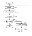
図2に、本実施の形態1のリダンダンシ制御回路100の動作フローチャートを示す。また、比較のため、特許文献1等の従来のリダンダンシ救済機能を持つ集積回路の動作フローチャートを図3に示す。まず、図3に示す従来の集積回路では、BISTを実行する(S201)。BISTの結果からリダンダンシ救済演算を行う(S202)。その演算結果に基づきヒューズカットを行う(S203)。このように、従来では、1回のヒューズカットによるリダンダンシ救済で完結してしまっている。
FIG. 2 shows an operation flowchart of the
これに対して、図2に示すリダンダンシ制御回路100では、BISTを実行する(S101)。BISTの結果からリダンダンシ救済演算を行う(S102)。その演算結果に基づきヒューズカットを行う(S103)。ここで、再ヒューズカットを行う場合(S104YES)、過去にカットされたヒューズのデータを読み込む(S105)。この過去のヒューズデータを基にリダンダンシ救済データを設定する(S106)。その後、S106で設定されたリダンダンシ救済データを基に、BISTを再実行する(S101)。
On the other hand, the
以降、S102、S103の処理を行い、再ヒューズカットを行わなくなる(S104NO)まで、繰り返す。このように、リダンダンシ制御回路100は、過去にカットされたヒューズのデータを利用してリダンダンシ救済処理が行われる。
Thereafter, the processes of S102 and S103 are performed, and the process is repeated until re-fuse cutting is not performed (NO in S104). As described above, the
従来のリダンダンシを持つメモリ回路に対する不良救済は、1つの条件で行なったテストで不良と検出された際の、不良情報をもとに、集積回路内でリダンダンシ救済情報を求めていた。そして、そのリダンダンシ救済情報に応じたヒューズをカットすることでリダンダンシ救済を行なっていた。このような方法では、複数のテスト条件において不良となる部分が変わる場合、各条件での不良情報を集積回路外に蓄積しておく必要がある。 In the conventional defect repair for a memory circuit having redundancy, redundancy repair information is obtained in the integrated circuit based on the defect information when a defect is detected in a test performed under one condition. Then, redundancy relief is performed by cutting a fuse according to the redundancy relief information. In such a method, when a defective part changes in a plurality of test conditions, it is necessary to store defect information for each condition outside the integrated circuit.
しかし、本実施の形態1のリダンダンシ制御回路100を組み込んだ集積回路では、1つの条件で行ったテスト結果による不良部分の救済情報を、カットしたヒューズのビット位置情報で保存する。そして、他の条件下でのテスト時に、カットしたヒューズの情報から過去の不良部分の救済情報をヒューズデータ読み出し回路160で読み出す。更に、読み出したデータをリダンダンシ救済演算データ変換回路170で、リダンダンシ救済データに変換する。その変換された過去のリダンダンシ救済データと、今回行ったテスト結果から、リダンダンシ救済演算を行う。この演算結果により、複数の条件下での不良救済を行う。このことにより、リダンダンシ制御回路100を組み込んだ集積回路は、1つの条件下のテスト結果による不良部分の救済情報をカットしたヒューズのビット位置情報で保存する。このため、集積回路の電源を切ったとしても、その不良部分の救済情報は、集積回路内に保持されることになる。よって、複数の条件下でのテスト結果によるリダンダンシ救済を当該集積回路内で処理可能となる。結果として、当該集積回路外に各条件下でのリダンダンシ救済データを蓄積する必要がなく、更に蓄積データを管理する必要もない。よって、テスト設備の削減と、テスト効率の向上が可能となる。
However, in the integrated circuit incorporating the
発明の実施の形態2
以下、本発明を適用した具体的な実施の形態2について、図面を参照しながら詳細に説明する。この実施の形態2で説明するリダンダンシ制御回路200は、実施の形態1と同様、当該リダンダンシ制御回路200が組み込まれる半導体集積回路が有するメモリ回路のリダンダンシを制御するものとする。図4に本実施の形態2にかかるリダンダンシ制御回路200を示す。
Hereinafter, a specific second embodiment to which the present invention is applied will be described in detail with reference to the drawings. As in the first embodiment, the
図4に示すように、リダンダンシ制御回路200は、BIST機能付リダンダンシ救済データ生成回路220と、ヒューズデータ変換回路130と、ヒューズカット回路140と、ヒューズ部150と、ヒューズデータ読み出し回路160と、リダンダンシ救済演算データ変換回路170とを有する。なお、図4に示された符号のうち、図1と同じ符号を付した構成は、図1と同じか又は類似の構成を示している。本実施の形態2では、実施の形態1と相違する箇所を重点的に説明し、その他の箇所は説明を省略する。
As shown in FIG. 4, the
実施の形態2のリダンダンシ制御回路200が実施の形態1と異なるのは、BIST回路110と、リダンダンシ救済データ生成回路120とが結合したBIST機能付リダンダンシ救済データ生成回路220を有している点である。それ以外は、実施の形態1のリダンダンシ制御回路100と同様である。
The
BIST機能付リダンダンシ救済データ生成回路220は、BIST部210と、リダンダンシ救済データ設定部122と、リダンダンシ救済データ保持部123とを有する。BIST部210は、実施の形態1のBIST回路110と同様の機能を有している。よって、このBIST機能付リダンダンシ救済データ生成回路220により、BIST実行中にリダンダンシ救済演算を行うことができる。また、BIST回路110と同様の機能を有するBIST部210を備えるため、BIST機能付リダンダンシ救済データ生成回路220には、実施の形態1でBIST回路110からの不良情報を記憶する不良情報記憶部121が要らない。
The redundancy repair
以下に、リダンダンシ制御回路200の動作を説明する。ただし、本例でも、実施の形態1と同様、複数の不良が発生している場合を想定する。また、リダンダンシ制御回路200が組み込まれる半導体集積回路のメモリ回路(不図示)には、リダンダンシ救済に使用可能な複数の冗長ロウ(第1の冗長ロウ、第2の冗長ロウ、・・・)が用意されているとする。
Hereinafter, the operation of the
第1の条件下において、メモリ回路のテスト及びリダンダンシ救済を行う。まず、BIST部210によるメモリ回路のテストが行われる。このテストで、まず最初に、ロウアドレスROW1で不良が検出された場合、直ちにリダンダンシ救済データ設定部122が処理を行う。そして、不良の検出されたロウアドレスROW1がリダンダンシ救済データ保持部123に、リダンダンシ救済データRQ1aとして保持される。なお、このリダンダンシ救済データRQ1aに格納されたロウアドレスROW1は、後に行われるヒューズカットにより第1の冗長ロウにより救済される。
Under the first condition, the memory circuit is tested and redundancy repair is performed. First, the memory circuit is tested by the
更にその後のテストで不良が検出された場合で、その不良ロウアドレスが、リダンダンシ救済データ格納場所RQ1に格納されている上記ロウアドレスROW1と一致したならば、リダンダンシ救済データ設定部122は、新たなリダンダンシ救済データを生成しない。つまり、リダンダンシ救済データ保持部123に、リダンダンシ救済データRQ1aのみが保持される。
Further, if a defect is detected in the subsequent test and the defective row address matches the row address ROW1 stored in the redundancy repair data storage location RQ1, the redundancy repair
反対に不良が検出された場合で、その不良ロウアドレスが、上記ロウアドレスROW1と一致しないロウアドレスROW2であったならば、リダンダンシ救済データ設定部122は、新たなリダンダンシ救済データRQ2aを設定する。そして、そのリダンダンシ救済データRQ2aが、リダンダンシ救済データ保持部123に保持される。リダンダンシ救済データ格納場所RQ2には、ロウアドレスROW2が格納されている。なお、このリダンダンシ救済データ格納場所RQ2に格納されたロウアドレスROW2は、後に行われるヒューズカットにより第2の冗長ロウにより救済される。また、リダンダンシ救済データRQ1a、RQ2aのヒューズ使用フラグは共に「0」である。
On the other hand, when a defect is detected and the defective row address is a row address ROW2 that does not match the row address ROW1, the redundancy repair
ヒューズデータ変換回路130は、リダンダンシ救済データ保持部123のリダンダンシ救済データRQ1aの不良ロウアドレスROW1を、不良を救済するためカットするヒューズのビット位置とその値に変換する。ヒューズカット回路140は、ヒューズデータ変換回路130が変換した値に応じた箇所のヒューズをカットする。このことにより、第1の冗長ロウを利用可能となり、第1の条件下におけるリダンダンシ救済が行われる。このようなヒューズカットを行うことにより、第1の条件下での不良救済情報がこのヒューズ部150に保存されたことになる。
The fuse
なお、リダンダンシ救済データ保持部123にリダンダンシ救済データRQ1a、RQ2aが保持されている場合、ヒューズデータ変換回路130とヒューズカット回路140の処理により、そのデータに対応したヒューズがカットされる。その結果、第1の冗長ロウ、第2の冗長ロウが利用可能となり、第1の条件下におけるリダンダンシ救済が行われる。
When the redundancy repair data RQ1a and RQ2a are held in the redundancy repair
次に、第2の条件下において、メモリ回路のテスト及びリダンダンシ救済を行う。まず、ヒューズデータ読み出し回路160は、第1の条件下で行ったリダンダンシ救済によりカットされたヒューズのビット位置情報を読み出す。リダンダンシ救済演算データ変換回路170は、ヒューズデータ読み出し回路160が読み出したヒューズのビット位置の値の情報をリダンダンシ救済データRQ1bに変換し、BIST機能付リダンダンシ救済データ生成回路220に送る。そして、このリダンダンシ救済データRQ1bが、リダンダンシ救済データ保持部123に保持される。このリダンダンシ救済データ保持部123に保持されたリダンダンシ救済データには、第1の条件下で格納したリダンダンシ救済データRQ1aと同じ不良ロウアドレスROW1が格納される。
Next, the memory circuit is tested and redundancy repaired under the second condition. First, the fuse
なお、もし第1の条件下で第1の冗長ロウ、第2の冗長ロウによるリダンダンシ救済が行われたならば、リダンダンシ救済データがRQ1a、RQ2aが格納していた不良ロウアドレスROW1、ROW2と同じものが、リダンダンシ救済データRQ1b、RQ2bにも格納される。なお、このリダンダンシ救済データRQ1、RQ2のヒューズ使用フラグは共に「1」である。 Note that if the redundancy repair by the first redundant row and the second redundant row is performed under the first condition, the redundancy repair data is the same as the defective row addresses ROW1 and ROW2 stored in RQ1a and RQ2a. Are also stored in the redundancy repair data RQ1b, RQ2b. Note that the fuse use flags of the redundancy repair data RQ1 and RQ2 are both “1”.
さらに、第2の条件下で、BIST部210によるメモリ回路のテストが行われる。このテスト結果で検出した不良ロウアドレスが、リダンダンシ救済データ保持部123に保持されているリダンダンシ救済データRQ1b(もしくは、RQ1b、RQ2b)の不良ロウアドレスと一致するなら、リダンダンシ救済データ設定部122は、新たなリダンダンシ救済を行わないと決定する。よって、この場合、その後において新たなヒューズカットは行われない。
Further, the memory circuit is tested by the
反対に、テスト結果で検出した不良ロウアドレスが、リダンダンシ救済データ保持部123に保持されているリダンダンシ救済データRQ1b(もしくは、RQ1b、RQ2b)の不良ロウアドレスと一致しないのもがあるなら、リダンダンシ救済データ設定部122は、その不良ロウアドレスを新たなリダンダンシ救済データRQ3aとして設定する。このリダンダンシ救済データRQ3aは、リダンダンシ救済データ保持部123に保持される。このリダンダンシ救済データRQ3aのヒューズ使用フラグは「0」である。よって、上述したのと同様の動作が行われ、新たにヒューズカットがヒューズデータ変換回路130とヒューズカット回路140の処理により行われる。このことにより、第2の条件下での不良救済情報がこのヒューズ部150に保存されたことになる。
On the contrary, if the defective row address detected from the test result does not match the defective row address of the redundancy repair data RQ1b (or RQ1b, RQ2b) held in the redundancy repair
更に、第3の条件下において、メモリ回路のテスト及びリダンダンシ救済を行い、上述したのと同様の処理を繰り返してもよい。このように、複数の条件下で発生する不良に対するリダンダンシ救済を行う。 Furthermore, under the third condition, the memory circuit may be tested and redundancy repaired, and the same processing as described above may be repeated. In this way, redundancy remedy for defects occurring under a plurality of conditions is performed.
図5に、本実施の形態2のリダンダンシ制御回路200の動作フローチャートを示す。図5に示すように、まず、BIST機能付リダンダンシ救済データ生成回路220により、BIST及びリダンダンシ救済演算を同時に行う(S301)。その演算結果に基づきヒューズカットを行う(S302)。ここで、再ヒューズカットを行う場合(S303YES)、過去にカットされたヒューズのデータを読み込む(S304)。この過去のヒューズデータを基にリダンダンシ救済データを設定する(S305)。その後、S305で設定されたリダンダンシ救済データを基に、BIST及びリダンダンシ救済演算を同時実行する(S301)。以降、S302の処理を行い、再ヒューズカットを行わなくなる(S303NO)まで、繰り返す。上記フローチャートからわかるように、実質的には図2で説明した実施の形態1のフローチャートのS101、S102の処理を同時に行っている点が本実施の形態2のフローチャートと異なる。
FIG. 5 shows an operation flowchart of the
以上のように、本実施の形態2のリダンダンシ制御回路200では、BISTを行うテスト回路とリダンダンシ救済演算を行う演算回路が同一回路内で構成されている。このため、実施の形態1で必要であった、不良情報記憶部111が必要なくなり、回路規模を削減することができる。更に、BISTで検出された不良情報を直ちにリダンダンシ救済データ設定部122で処理できるメリットもある。
As described above, in the
発明の実施の形態3 Embodiment 3 of the Invention
以下、本発明を適用した具体的な実施の形態3について、図面を参照しながら詳細に説明する。この実施の形態2で説明するリダンダンシ制御回路300は、実施の形態1、2と同様、当該リダンダンシ制御回路300が組み込まれる半導体集積回路が有するメモリ回路のリダンダンシを制御するものとする。図6に本実施の形態3にかかるリダンダンシ制御回路300を示す。
Hereinafter, a specific third embodiment to which the present invention is applied will be described in detail with reference to the drawings. As in the first and second embodiments, the
図6に示すように、リダンダンシ制御回路300は、BIST機能付リダンダンシ救済データ生成回路220と、ヒューズデータ変換回路330と、ヒューズカット回路140と、ヒューズ部150と、ヒューズデータ読み出し回路160と、リダンダンシ救済演算データ変換回路370とを有する。なお、図6に示された符号のうち、図1、図4と同じ符号を付した構成は、図1、図4と同じか又は類似の構成を示している。本実施の形態3では、実施の形態1、2と相違する箇所を重点的に説明し、その他の箇所は説明を省略する。
As shown in FIG. 6, the
実施の形態3のリダンダンシ制御回路300が実施の形態1、2と異なるのは、ヒューズデータ変換回路330と、リダンダンシ救済演算データ変換回路370とである。それ以外は、実施の形態1、2のリダンダンシ制御回路100、200と同様である。但し、BIST機能付リダンダンシ救済データ生成回路220のリダンダンシ救済データ保持部111に保持されるリダンダンシ救済データは、実施の形態1、2と異なり、不良IOビット位置の情報が保持される。ここで、不良IOビット位置の情報とは、以下のようなものであるとする。
The
例えば、メモリ回路が8ビットのIOデータを格納できる構成(以下、IOビットと称す)であるとする。そして、そのIOビットの5ビット目で不良が検出された場合、不良IOビット位置の情報として、「00010000」という8ビットのデータが生成される。これは、不良ビットの位置データとして、LSB(右端側)から5ビット目が、値「1」となっている。なお、メモリ回路に不良ビットがなければ、不良IOビット位置の情報として、「00000000」という全てのビット値が「0」となる8ビットのデータが生成される。但し、これは一例であるため、不良IOビットの位置が確定できるものであれば良い。よって、不良IOビット位置の情報は、上記構成にとらわれないものとする。 For example, it is assumed that the memory circuit has a configuration capable of storing 8-bit IO data (hereinafter referred to as an IO bit). When a defect is detected at the fifth bit of the IO bit, 8-bit data “00010000” is generated as information on the position of the defective IO bit. This is the value “1” in the fifth bit from the LSB (right end side) as the position data of the defective bit. If there is no defective bit in the memory circuit, 8-bit data in which all bit values “00000000” are “0” is generated as information on the defective IO bit position. However, since this is an example, it is sufficient if the position of the defective IO bit can be determined. Therefore, the information on the defective IO bit position is not limited to the above configuration.
ヒューズデータ変換回路330は、IOアドレス変換部331と、ヒューズビット変換部332とを有する。IOアドレス変換部331は、リダンダンシ救済データ保持部123のリダンダンシ救済データである不良IOビット位置の情報をアドレスの値に変換する。ヒューズビット変換部332は、IOアドレス変換部331からのアドレスの値の情報に応じて、リダンダンシ救済に対応するヒューズのビット位置とその値に変換し、ヒューズカット回路140に送る。ヒューズカット回路140は、このヒューズのビット位置の値の情報に応じたヒューズをカットする。
The fuse
リダンダンシ救済演算データ変換回路370は、IOビット変換部371と、リダンダンシ救済アドレス変換部372とを有する。リダンダンシ救済アドレス変換部372は、ヒューズデータ読み出し回路160からのヒューズデータを不良IOビットの位置に対応するアドレス情報に変換する。IOビット変換部371は、このアドレス情報を不良IOビット位置の情報に変換し、リダンダンシ救済データ保持部123へ送る。
The redundancy repair operation
以下に、リダンダンシ制御回路300の動作を説明する。本例では、メモリ回路(不図示)の不良をビット単位でリダンダンシ救済する場合を示す。但し、説明を簡略化するため、メモリ回路は、8ビットのIOデータを格納できる構成となっているものとする。また、このメモリ回路には、リダンダンシ救済に使用可能な複数の冗長IOビット(第1の冗長IOビット、第2の冗長IOビット、・・・)が用意されているとする。
Hereinafter, the operation of the
第1の条件下において、メモリ回路のテスト及びリダンダンシ救済を行う。まず、BIST部210によるメモリ回路のテストが行われる。このテストで、IOビットの5ビット目で不良が検出された場合、直ちにリダンダンシ救済データ設定部122が処理を行う。このとき、不良ビットのデータとして、値が「1」のIOデータが生成される。具体的には、「00010000」のようにLSB(右端側)から5ビット目が値「1」として表現された8ビットデータが生成される。そして、この不良の検出された不良ビットのデータがリダンダンシ救済データ保持部123に、リダンダンシ救済データとして保持される。あるいは、BISTで発見された不良IOビットのデータは、一端パイプラインレジスタに保持して、その保持時間の間に、リダンダンシ救済データ保持部123に保存してもよい。以下の説明では、第1の条件下におけるテスト結果から設定されるリダンダンシ救済データをRB1aまたはRB1bと表記し、第1の条件下におけるテスト結果から設定されるリダンダンシ救済データを含んで第2の条件下におけるテスト結果から設定されるリダンダンシ救済データをRB2aまたはRB2bと表記するものとする。ここで、RB1aとRB2aは、リダンダンシ救済データ設定部122で直接生成されたデータを示し、RB1bとRB2bは、ヒューズから読み出したデータをリダンダンシ救済データに変換したデータを示している。
Under the first condition, the memory circuit is tested and redundancy repair is performed. First, the memory circuit is tested by the
ヒューズデータ変換回路330は、リダンダンシ救済データ保持部123のリダンダンシ救済データRB1aの不良IOビット情報を、不良を救済するためカットするヒューズのビット位置とその値に変換する。ヒューズカット回路140は、ヒューズデータ変換回路130が変換した値に応じた箇所のヒューズをカットする。このことにより、第1の冗長IOビットを利用可能となり、第1の条件下におけるリダンダンシ救済が行われる。このようなヒューズカットを行うことにより、第1の条件下での不良救済情報がこのヒューズ部150に保存されたことになる。
The fuse
次に、第2の条件下において、メモリ回路のテスト及びリダンダンシ救済を行う。まず、ヒューズデータ読み出し回路160は、第1の条件下で行ったリダンダンシ救済によりカットされたヒューズのビット位置情報を読み出す。リダンダンシ救済演算データ変換回路370は、ヒューズデータ読み出し回路160が読み出したヒューズのビット位置の値の情報をリダンダンシ救済データRB1bに変換し、BIST機能付リダンダンシ救済データ生成回路220に送る。そして、このリダンダンシ救済データRB1bが、リダンダンシ救済データ保持部123に保持される。このリダンダンシ救済データ保持部123に保持されたリダンダンシ救済データには、第1の条件下で格納したリダンダンシ救済データRB1aと同じ不良IOビット位置の情報が格納される。具体的には、上述した不良IOビット位置の情報と同じ、「00010000」という8ビットデータである。
Next, the memory circuit is tested and redundancy repaired under the second condition. First, the fuse
さらに、第2の条件下で、BIST部210によるメモリ回路のテストが行われる。このテスト結果で検出した不良IOビット位置の情報が、リダンダンシ救済データ保持部123に保持されているリダンダンシ救済データRB1bの不良IOビット位置の情報と一致するなら、リダンダンシ救済データ設定部122は、新たなリダンダンシ救済を行わないと決定する。よって、この場合、その後において新たなヒューズカットは行われない。
Further, the memory circuit is tested by the
反対に、テスト結果で検出した不良IOビット位置の情報が、リダンダンシ救済データ保持部123に保持されているリダンダンシ救済データRB1bの不良IOビット位置の情報と一致しないのもがあるなら、リダンダンシ救済データ設定部122は、その不良IOビット位置の情報とリダンダンシ救済データRB1bの不良IOビット位置の情報とのOR演算を行い、新たなリダンダンシ救済データRB2aを生成する。
On the other hand, if the information on the defective IO bit position detected by the test result does not match the information on the defective IO bit position of the redundancy repair data RB1b held in the redundancy repair
具体的に説明すると、第2の条件下のテストで、IOビットの3ビット目と5ビット目で不良が検出された場合、不良IOビット位置の情報として「00010100」が生成される。この不良IOビット位置の情報「00010100」と、リダンダンシ救済データRB1bの不良IOビット位置の情報「00010000」のOR演算を行い、新たなリダンダンシ救済データRB2aとして不良IOビット位置の情報「00010100」を生成する。 More specifically, when a defect is detected in the third and fifth bits of the IO bit in the test under the second condition, “00010100” is generated as information on the defective IO bit position. An OR operation is performed on the defective IO bit position information “00010100” and the redundant IO bit position information “00010000” of the redundancy repair data RB1b to generate the defective IO bit position information “00010100” as new redundancy repair data RB2a. To do.
このリダンダンシ救済データRB2aの不良IOビット位置の情報「00010100」に基づいて、新たにヒューズカットがヒューズデータ変換回路330とヒューズカット回路140の処理により行われる。このことにより、第2の冗長IOビットを利用可能となり、第2の条件下におけるリダンダンシ救済が行われる。よって、第2の条件下での不良救済情報がこのヒューズ部150に保存されたことになる。
Based on the information “00010100” of the defective IO bit position of the redundancy repair data RB2a, a new fuse cut is performed by the processing of the fuse
なお、リダンダンシ救済データ保持部が、不良IOビット位置の情報しか持たず、救済されたIOビットに対するどのヒューズがカットされているかの情報を持っていない場合、そのヒューズカット情報を保持している回路(以下、ヒューズカット情報保持回路と称す)から、情報を取り出し、未カットのIOビットに対するアドレス情報に変換し、ヒューズカットを行なうようにしてもよい。ヒューズカット情報保持回路としては、リダンダンシ救済演算データ変換回路370に変換前のIOビットを現すアドレスを保持しておく等がある。この保持データをDQとして、図6に示す。また、実施の形態1、2と同様、ヒューズ使用フラグをリダンダンシ救済データに格納してもよい。
If the redundancy repair data holding unit has only information on the defective IO bit position and does not have information on which fuse is cut for the repaired IO bit, the circuit holding the fuse cut information Information may be extracted from (hereinafter referred to as a fuse cut information holding circuit), converted into address information for an uncut IO bit, and a fuse cut may be performed. As the fuse cut information holding circuit, there is a method in which the redundancy relief operation
更に、第3の条件下において、メモリ回路のテスト及びリダンダンシ救済を行い、上述したのと同様の処理を繰り返してもよい。このように、複数の条件下で発生する不良に対するリダンダンシ救済を行う。 Furthermore, under the third condition, the memory circuit may be tested and redundancy repaired, and the same processing as described above may be repeated. In this way, redundancy remedy for defects occurring under a plurality of conditions is performed.
ここで、メモリ回路のテストは、通常、1サイクルで1アドレスずつしか行なわれない。しかしながら、IOに関しては、ビット数分(上述した例では、8ビット)全ビット同時にテストが行われる。このため、BISTの検査結果から、どのビットに不良があり、それが過去に既に検出された不良と一致するか否かを判断するには、多数のクロックサイクルを必要とする。また、1回のBISTにより検出する不良ビットの数も1つとは限らない。しかし、IO(IOデータ)に対しては、ビット数分(上述した例では、8ビット)全ビット同時に行なわれる。 Here, the test of the memory circuit is normally performed only one address at a time in one cycle. However, for IO, all the bits are tested simultaneously for the number of bits (8 bits in the above example). For this reason, it takes a large number of clock cycles to determine from the BIST inspection results which bits are defective and whether or not they match the defects already detected in the past. Also, the number of defective bits detected by one BIST is not necessarily one. However, with respect to IO (IO data), all bits are simultaneously performed for the number of bits (8 bits in the above example).
本実施の形態3では、このことを利用して、IO(IOデータ)のリダン救済演算の場合、ビット数分で不良箇所の検出を行い、その不良箇所をIOビット数分のデータのビット位置(上述した例の「00010100」の値「1」の箇所)で表し、BIST終了後に、そのビット位置に対応するアドレスに変換する。このことにより、テスト及びリダンダンシ救済の効率化が上昇する効果が得られる。 In the third embodiment, by utilizing this fact, in the case of IO (IO data) redundancy repair operation, a defective portion is detected by the number of bits, and the defective portion is detected as the bit position of the data corresponding to the number of IO bits. (The location of the value “1” of “00010100” in the above example), and after the BIST ends, the address is converted to an address corresponding to the bit position. As a result, an effect of increasing the efficiency of the test and redundancy repair can be obtained.
なお、本発明は上記実施の形態に限られたものでなく、趣旨を逸脱しない範囲で適宜変更することが可能である。 Note that the present invention is not limited to the above-described embodiment, and can be changed as appropriate without departing from the spirit of the present invention.
100、200、300 リダンダンシ制御回路
110 BIST回路
120 リダンダンシ救済データ生成回路
121 不良情報記憶部
122 リダンダンシ救済データ設定部
123 リダンダンシ救済データ保持部
130、330 ヒューズデータ変換回路
140 ヒューズカット回路
150 ヒューズ部
160 ヒューズデータ読み出し回路
170、370 リダンダンシ救済演算データ変換回路
210 BIST部
220 BIST機能付リダンダンシ救済データ生成回路
331 IOアドレス変換回路
332 ヒューズビット変換回路
371 IOビット変換回路
372 リダンダンシ救済アドレス変換回路
100, 200, 300
Claims (7)
複数のヒューズと、
前記複数のヒューズのうち、対応するヒューズが第1の状態となることで、前記複数のメモリセルにある不良セルを救済する機能を有する冗長メモリと、を有する集積回路であって、
既に救済され、第1の不良セルに対応した前記第1の状態となっているヒューズの位置情報から、前記第1の不良セルの第1の情報を生成するヒューズデータ変換回路と、
前記複数のメモリセルのテスト結果により第2の不良セルを検出すると、その検出した第2の不良セルの第2の情報と、前記第1の不良セルの第1の情報とに応じて、前記第2の不良セルを救済するための救済情報を生成する救済データ生成回路と、
前記救済データ生成回路が生成した救済情報に応じて、前記複数のヒューズのうち、所定のヒューズを第1の状態とするヒューズ状態変更回路と、
を有する集積回路。 A plurality of memory cells;
Multiple fuses,
A redundant memory having a function of relieving a defective cell in the plurality of memory cells by causing a corresponding fuse among the plurality of fuses to be in a first state;
A fuse data conversion circuit that generates first information of the first defective cell from position information of the fuse that has already been relieved and is in the first state corresponding to the first defective cell;
When a second defective cell is detected based on the test results of the plurality of memory cells, the second information on the detected second defective cell and the first information on the first defective cell are used. A repair data generation circuit for generating repair information for repairing the second defective cell;
A fuse state changing circuit for setting a predetermined fuse among the plurality of fuses to a first state in accordance with the repair information generated by the repair data generating circuit;
An integrated circuit.
前記ヒューズデータ変換回路からの前記第1の不良セルの第1の情報を保持する保持部と、
前記複数のメモリセルのテスト結果である前記第2の不良セルの第2の情報と、前記保持部が保持する前記第1の不良セルの第1の情報とのデータ値が異なる場合、前記第2の不良セルの第2の情報に応じた救済情報を設定する救済データ設定部と、を有する
請求項1に記載の集積回路。 The relief data generation circuit includes:
A holding unit for holding first information of the first defective cell from the fuse data conversion circuit;
When the data value of the second information of the second defective cell, which is the test result of the plurality of memory cells, and the first information of the first defective cell held by the holding unit are different from each other, The integrated circuit according to claim 1, further comprising: a repair data setting unit that sets repair information according to second information of two defective cells.
前記複数のメモリセルのテストを行うテスト部を更に有する
請求項2に記載の集積回路。 The relief data generation circuit includes:
The integrated circuit according to claim 2, further comprising a test unit that tests the plurality of memory cells.
前記救済データ生成回路は、
前記テスト回路のテスト結果である前記第2の不良セルの第2の情報を記憶する記憶部と、
前記ヒューズデータ変換回路からの前記第1の不良セルの第1の情報を保持する保持部と、
前記記憶部が記憶する前記第2の不良セルの第2の情報と、前記保持部が保持する前記第1の不良セルの第1の情報とのデータ値が異なる場合、前記第2の不良セルの第2の情報に応じた救済情報を設定する救済データ設定部と、を有する
請求項1に記載の集積回路。 A test circuit for testing the plurality of memory cells;
The relief data generation circuit includes:
A storage unit that stores second information of the second defective cell that is a test result of the test circuit;
A holding unit for holding first information of the first defective cell from the fuse data conversion circuit;
When the data value of the second information of the second defective cell stored in the storage unit and the first information of the first defective cell stored in the holding unit are different, the second defective cell The integrated circuit according to claim 1, further comprising: a relief data setting unit that sets relief information according to the second information.
請求項1〜請求項4のいずれか1項に記載の集積回路。 The integrated circuit according to claim 1, wherein the first state is a state in which a fuse is cut.
前記第1の不良セルに対応してカットされたヒューズの位置情報を読み出すヒューズデータ読み出し回路と、
前記ヒューズデータ読み出し回路が読み出したカットされたヒューズの位置情報から、前記第1の不良セルの第1の情報に変換する救済データ変換回路と、を有する
請求項5に記載の集積回路。 The fuse data conversion circuit
A fuse data read circuit for reading position information of a fuse cut corresponding to the first defective cell;
The integrated circuit according to claim 5, further comprising: a repair data conversion circuit that converts the position information of the cut fuse read by the fuse data read circuit into the first information of the first defective cell.
前記救済データ生成回路からの前記救済情報に応じて、カットするヒューズの位置情報を生成するヒューズデータ変換回路と、
前記ヒューズデータ変換回路からのヒューズの位置情報に応じたヒューズをカットするヒューズカット回路と、を有する
請求項5に記載の集積回路。 The fuse state change circuit
A fuse data conversion circuit for generating position information of a fuse to be cut in accordance with the relief information from the relief data generation circuit;
The integrated circuit according to claim 5, further comprising: a fuse cut circuit that cuts a fuse in accordance with fuse position information from the fuse data conversion circuit.
Priority Applications (2)
| Application Number | Priority Date | Filing Date | Title |
|---|---|---|---|
| JP2009089878A JP2010244596A (en) | 2009-04-02 | 2009-04-02 | Integrated circuit |
| US12/662,040 US8238177B2 (en) | 2009-04-02 | 2010-03-29 | Integrated circuit |
Applications Claiming Priority (1)
| Application Number | Priority Date | Filing Date | Title |
|---|---|---|---|
| JP2009089878A JP2010244596A (en) | 2009-04-02 | 2009-04-02 | Integrated circuit |
Publications (2)
| Publication Number | Publication Date |
|---|---|
| JP2010244596A true JP2010244596A (en) | 2010-10-28 |
| JP2010244596A5 JP2010244596A5 (en) | 2012-04-05 |
Family
ID=42826081
Family Applications (1)
| Application Number | Title | Priority Date | Filing Date |
|---|---|---|---|
| JP2009089878A Pending JP2010244596A (en) | 2009-04-02 | 2009-04-02 | Integrated circuit |
Country Status (2)
| Country | Link |
|---|---|
| US (1) | US8238177B2 (en) |
| JP (1) | JP2010244596A (en) |
Families Citing this family (9)
| Publication number | Priority date | Publication date | Assignee | Title |
|---|---|---|---|---|
| JP5664204B2 (en) * | 2010-12-15 | 2015-02-04 | 富士通株式会社 | Semiconductor memory |
| JP6063679B2 (en) * | 2012-09-10 | 2017-01-18 | ルネサスエレクトロニクス株式会社 | Semiconductor device |
| KR20150006167A (en) * | 2013-07-08 | 2015-01-16 | 에스케이하이닉스 주식회사 | Semiconductor system and repair memthod of the same |
| KR20160048584A (en) * | 2014-10-24 | 2016-05-04 | 에스케이하이닉스 주식회사 | Semiconductor device |
| KR20160138617A (en) * | 2015-05-26 | 2016-12-06 | 에스케이하이닉스 주식회사 | Smart self repair device and method |
| KR20160148347A (en) * | 2015-06-16 | 2016-12-26 | 에스케이하이닉스 주식회사 | Self repair device and method |
| KR20180082875A (en) * | 2017-01-11 | 2018-07-19 | 에스케이하이닉스 주식회사 | E-fuse circuit |
| JP2018133764A (en) * | 2017-02-17 | 2018-08-23 | 株式会社リコー | Redundant configuration system, changeover method, information processing system, and program |
| KR20220048735A (en) * | 2020-10-13 | 2022-04-20 | 삼성전자주식회사 | Test method of memory device, memory built-in self test(MBIST) circuit and memory device for short test time |
Citations (1)
| Publication number | Priority date | Publication date | Assignee | Title |
|---|---|---|---|---|
| JP2002150789A (en) * | 2000-11-09 | 2002-05-24 | Hitachi Ltd | Non-volatile semiconductor memory |
Family Cites Families (6)
| Publication number | Priority date | Publication date | Assignee | Title |
|---|---|---|---|---|
| US5550394A (en) * | 1993-06-18 | 1996-08-27 | Texas Instruments Incorporated | Semiconductor memory device and defective memory cell correction circuit |
| US5657281A (en) * | 1996-03-11 | 1997-08-12 | Cirrus Logic, Inc. | Systems and methods for implementing inter-device cell replacements |
| JP2002109899A (en) * | 2000-07-26 | 2002-04-12 | Mitsubishi Electric Corp | Semiconductor storage device and semiconductor integrated circuit device equipped with the same |
| JP2003196995A (en) * | 2001-12-26 | 2003-07-11 | Mitsubishi Electric Corp | Semiconductor memory and its test method |
| JP2004234729A (en) * | 2003-01-29 | 2004-08-19 | Renesas Technology Corp | Semiconductor memory device |
| JP2007323726A (en) | 2006-05-31 | 2007-12-13 | Matsushita Electric Ind Co Ltd | Semiconductor device |
-
2009
- 2009-04-02 JP JP2009089878A patent/JP2010244596A/en active Pending
-
2010
- 2010-03-29 US US12/662,040 patent/US8238177B2/en active Active
Patent Citations (1)
| Publication number | Priority date | Publication date | Assignee | Title |
|---|---|---|---|---|
| JP2002150789A (en) * | 2000-11-09 | 2002-05-24 | Hitachi Ltd | Non-volatile semiconductor memory |
Also Published As
| Publication number | Publication date |
|---|---|
| US8238177B2 (en) | 2012-08-07 |
| US20100254205A1 (en) | 2010-10-07 |
Similar Documents
| Publication | Publication Date | Title |
|---|---|---|
| JP2010244596A (en) | Integrated circuit | |
| US7373573B2 (en) | Apparatus and method for using a single bank of eFuses to successively store testing data from multiple stages of testing | |
| JP5127737B2 (en) | Semiconductor device | |
| US7512001B2 (en) | Semiconductor memory device, test system including the same and repair method of semiconductor memory device | |
| JP2006228330A (en) | Semiconductor memory device | |
| JP2010123159A (en) | Semiconductor integrated circuit | |
| US9978463B2 (en) | Semiconductor apparatus and repair method thereof | |
| JP2004310951A (en) | Semiconductor integrated circuit and its inspection method | |
| JP2006302129A (en) | Computer system and defect relief method for memory | |
| JP5611916B2 (en) | Semiconductor integrated circuit | |
| JP5439974B2 (en) | Semiconductor device and method of writing defective portion information | |
| JP4880999B2 (en) | Semiconductor integrated circuit and inspection method thereof | |
| TW201032237A (en) | Semiconductor test system with self-inspection of memory repair analysis | |
| JP4891748B2 (en) | Semiconductor integrated circuit and test method thereof | |
| US10043588B2 (en) | Memory device | |
| KR100944325B1 (en) | Repair fuse device | |
| US20100138707A1 (en) | Processor and method for controlling storage-device test unit | |
| JP2013131273A (en) | Semiconductor integrated circuit and method of testing semiconductor integrated circuit | |
| JP4761995B2 (en) | Semiconductor integrated circuit and test method thereof | |
| KR20080111329A (en) | Semiconductor memory device having electrical fuse data and electrical fuse data fetching method thereof | |
| US7830710B2 (en) | Semiconductor memory device | |
| JP2005004876A (en) | Semiconductor memory device and its evaluating method | |
| JP2011034642A (en) | Memory test circuit, semiconductor integrated circuit, and memory test method | |
| JP4993175B2 (en) | Memory inspection device | |
| JP2008084425A (en) | Test method of semiconductor device |
Legal Events
| Date | Code | Title | Description |
|---|---|---|---|
| A521 | Request for written amendment filed |
Free format text: JAPANESE INTERMEDIATE CODE: A523 Effective date: 20120220 |
|
| A621 | Written request for application examination |
Free format text: JAPANESE INTERMEDIATE CODE: A621 Effective date: 20120220 |
|
| A977 | Report on retrieval |
Free format text: JAPANESE INTERMEDIATE CODE: A971007 Effective date: 20130218 |
|
| A131 | Notification of reasons for refusal |
Free format text: JAPANESE INTERMEDIATE CODE: A131 Effective date: 20130226 |
|
| A02 | Decision of refusal |
Free format text: JAPANESE INTERMEDIATE CODE: A02 Effective date: 20130625 |