JP2010062563A - 局所的に不動態化されたゲルマニウムオンインシュレータ基板の製造方法 - Google Patents
局所的に不動態化されたゲルマニウムオンインシュレータ基板の製造方法 Download PDFInfo
- Publication number
- JP2010062563A JP2010062563A JP2009200482A JP2009200482A JP2010062563A JP 2010062563 A JP2010062563 A JP 2010062563A JP 2009200482 A JP2009200482 A JP 2009200482A JP 2009200482 A JP2009200482 A JP 2009200482A JP 2010062563 A JP2010062563 A JP 2010062563A
- Authority
- JP
- Japan
- Prior art keywords
- substrate
- plasma
- layer
- germanium
- region
- Prior art date
- Legal status (The legal status is an assumption and is not a legal conclusion. Google has not performed a legal analysis and makes no representation as to the accuracy of the status listed.)
- Granted
Links
Images


Classifications
-
- H10P14/6316—
-
- H—ELECTRICITY
- H10—SEMICONDUCTOR DEVICES; ELECTRIC SOLID-STATE DEVICES NOT OTHERWISE PROVIDED FOR
- H10D—INORGANIC ELECTRIC SEMICONDUCTOR DEVICES
- H10D62/00—Semiconductor bodies, or regions thereof, of devices having potential barriers
- H10D62/80—Semiconductor bodies, or regions thereof, of devices having potential barriers characterised by the materials
- H10D62/83—Semiconductor bodies, or regions thereof, of devices having potential barriers characterised by the materials being Group IV materials, e.g. B-doped Si or undoped Ge
-
- H10P14/6319—
-
- H10P14/68—
-
- H10P90/1906—
-
- H10P90/1916—
-
- H10W10/014—
-
- H10W10/061—
-
- H10W10/17—
-
- H10W10/181—
Landscapes
- Engineering & Computer Science (AREA)
- Recrystallisation Techniques (AREA)
- General Physics & Mathematics (AREA)
- Physics & Mathematics (AREA)
- Manufacturing & Machinery (AREA)
- Computer Hardware Design (AREA)
- Microelectronics & Electronic Packaging (AREA)
- Power Engineering (AREA)
- Insulated Gate Type Field-Effect Transistor (AREA)
- Condensed Matter Physics & Semiconductors (AREA)
- Thin Film Transistor (AREA)
- Element Separation (AREA)
- Metal-Oxide And Bipolar Metal-Oxide Semiconductor Integrated Circuits (AREA)
Abstract
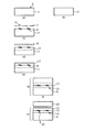
【解決手段】 本発明は、局所的に不動態化されたゲルマニウムオンインシュレータ基板を製造するための方法に関し、電子の高移動度を実現するために、窒化された領域が局所化された位置に形成される。窒化はプラズマ処理によって実現される。
【選択図】 図1
Description
Claims (21)
- 局所的に不動態化されたゲルマニウムオンインシュレータ基板を製造する方法であって、
a)Ge含有層、特にSiGe層若しくはエピタキシャルGe層を備える基板、又はGe基板を、ソース基板として形成するステップと、
b)不動態化された領域、特にGeOxNyを含む領域を局所的に形成するステップと、
を備える、方法。 - 前記ステップb)が、前記ソース基板上にパターニングされたマスクを形成する工程を備える、請求項1に記載の方法。
- 前記ステップb)が、窒化によって不動態化する工程を更に備える、請求項1又は2に記載の方法。
- 前記ステップb)が、プラズマ、特にNH3プラズマ、N2プラズマ、又はN2Oプラズマを用いて、前記ソース基板を処理する工程を備える、請求項1〜3の何れか一項に記載の方法。
- 前記ステップb)が、酸素プラズマ及び/又はアルゴンプラズマを、特に前記NH3プラズマ、前記N2プラズマ、又は前記N2Oプラズマを印加する前に、印加する工程を更に備える、請求項1〜4の何れか一項に記載の方法。
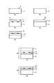
- 前記ステップb)の前又は後に、c)前記ソース基板内に所定の分離領域を形成するステップを更に備える、請求項1〜5の何れか一項に記載の方法。
- 前記ステップc)の前又は後に、d)絶縁体層、特に酸化層を前記ソース基板上に形成するステップを更に備える、請求項1〜6の何れか一項に記載の方法。
- 前記局所的に不動態化された領域を、特に約600℃で1時間以上アニールするステップを更に備える、請求項1〜7の何れか一項に記載の方法。
- e)前記ソース基板をハンドル基板に、好ましくはボンディングによって取り付けるステップと、
f)前記所定の分離領域で前記ソース基板を分離して、前記局所的に不動態化されたゲルマニウムオンインシュレータ基板を得るステップと、
を更に備える、請求項1〜8の何れか一項に記載の方法。 - 前記ステップe)の前に、g)絶縁体層、特に酸化層を前記ハンドル基板上に形成するステップを更に備える、請求項9に記載の方法。
- 前記ステップe)の前に、h)プラズマ、特に酸素プラズマ及び/又はNH3プラズマ、N2プラズマ、又はN2Oプラズマを用いて前記ハンドル基板を活性化するステップを更に備える、請求項9又は10に記載の方法。
- 前記ステップe)が、前記ソース基板に対する前記プラズマス処理ステップb)及び前記ハンドル基板の前記プラズマ処理ステップh)の直後に、且つ更なるプロセスステップを介在することなく、行われる、請求項9〜11に記載の方法。
- 前記マスクが、一以上のシャドーマスク、特にテフロンマスク又は金属マスクであり、又は堆積されたマスク、特にフォトレジストベースマスク又はGeO2マスクである、請求項2〜12の何れか一項に記載の方法。
- 前記マスク形成工程は、
前記ソース基板上にGeOx層を形成することと、
フォトレジスト層を形成することと、
前記フォトレジスト層をナノインプリンティングすることと、
プラズマエッチング、特に反応性イオンエッチングによってパターンを形成することと、を備える、請求項13に記載の方法。 - 前記ソース基板内又は前記ソース基板上に合わせマークを形成するステップを更に備える、請求項1〜14の何れか一項に記載の方法。
- 前記合わせマーク形成ステップが、前記ソース基板パターン内に凹部のパターンを形成するステップを備える、請求項15に記載の方法。
- 絶縁体層、特にSiO2層が前記凹部内に形成される、請求項16に記載の方法。
- 前記ステップc)が行われ、前記所定の分離領域が前記ソース基板内の前記凹部を横切る、請求項15〜17の何れか一項に記載の方法。
- 局所的に不動態化された領域をGe層内又はGe層上に備えており、請求項1〜18の何れか一項に記載の方法によって得られるゲルマニウムオンインシュレータ基板。
- 前記局所的に不動態化された領域の位置を特定するように構成且つ配置された合わせマークを更に備える、請求項19に記載のゲルマニウムオンインシュレータ基板。
- ゲルマニウムオンインシュレータ基板内又はゲルマニウムオンインシュレータ基板上に、n−MOSデバイス構造及びp−MOSデバイス構造を備える電子デバイスにおいて、
前記n−MOSデバイス構造が、局所化されていると共に不動態化された領域、特にGeOxNyを含む領域上に形成されており、
前記p−MOSデバイス構造が、前記ゲルマニウムオンインシュレータ基板の他の領域上に形成されていることを特徴とする電子デバイス。
Applications Claiming Priority (2)
| Application Number | Priority Date | Filing Date | Title |
|---|---|---|---|
| EP20080290827 EP2161742A1 (en) | 2008-09-03 | 2008-09-03 | Method for Fabricating a Locally Passivated Germanium-on-Insulator Substrate |
| EP08290827.8 | 2008-09-03 |
Publications (2)
| Publication Number | Publication Date |
|---|---|
| JP2010062563A true JP2010062563A (ja) | 2010-03-18 |
| JP5240578B2 JP5240578B2 (ja) | 2013-07-17 |
Family
ID=40085584
Family Applications (1)
| Application Number | Title | Priority Date | Filing Date |
|---|---|---|---|
| JP2009200482A Expired - Fee Related JP5240578B2 (ja) | 2008-09-03 | 2009-08-31 | 局所的に不動態化されたゲルマニウムオンインシュレータ基板の製造方法 |
Country Status (3)
| Country | Link |
|---|---|
| US (2) | US8372733B2 (ja) |
| EP (1) | EP2161742A1 (ja) |
| JP (1) | JP5240578B2 (ja) |
Families Citing this family (7)
| Publication number | Priority date | Publication date | Assignee | Title |
|---|---|---|---|---|
| US8298923B2 (en) * | 2010-10-27 | 2012-10-30 | International Business Machinces Corporation | Germanium-containing release layer for transfer of a silicon layer to a substrate |
| US8772873B2 (en) | 2011-01-24 | 2014-07-08 | Tsinghua University | Ge-on-insulator structure and method for forming the same |
| CN102157432A (zh) * | 2011-01-24 | 2011-08-17 | 清华大学 | GeOI结构及其形成方法 |
| US10020187B2 (en) | 2012-11-26 | 2018-07-10 | Applied Materials, Inc. | Apparatus and methods for backside passivation |
| CN103078009B (zh) * | 2013-01-14 | 2015-05-27 | 中国科学院上海微系统与信息技术研究所 | 基于免等离子工艺降低暗电流的光电探测器芯片制作方法 |
| CN103928297B (zh) * | 2013-12-28 | 2017-04-26 | 华中科技大学 | 锗硅纳米低维结构的可控制备方法及产品 |
| CN105742180A (zh) * | 2016-03-11 | 2016-07-06 | 成都海威华芯科技有限公司 | GaN HEMT器件的制作方法 |
Citations (4)
| Publication number | Priority date | Publication date | Assignee | Title |
|---|---|---|---|---|
| JP2001111014A (ja) * | 1999-08-30 | 2001-04-20 | Lucent Technol Inc | ボンデッドウエハおよびその製造方法およびそれにより製造される集積回路 |
| JP2006148066A (ja) * | 2004-11-19 | 2006-06-08 | Soi Tec Silicon On Insulator Technologies Sa | ゲルマニウム・オン・インシュレータ(GeOI)型ウェーハの製造方法 |
| WO2007045759A1 (fr) * | 2005-10-19 | 2007-04-26 | S.O.I. Tec Silicon On Insulator Technologies | Traitement d'une couche de germanium collee a un substrat |
| JP2008516443A (ja) * | 2004-10-06 | 2008-05-15 | コミツサリア タ レネルジー アトミーク | 様々な絶縁領域及び/又は局所的な垂直導電領域を有する混合積層構造物を製造する方法 |
Family Cites Families (8)
| Publication number | Priority date | Publication date | Assignee | Title |
|---|---|---|---|---|
| US6855436B2 (en) * | 2003-05-30 | 2005-02-15 | International Business Machines Corporation | Formation of silicon-germanium-on-insulator (SGOI) by an integral high temperature SIMOX-Ge interdiffusion anneal |
| US7049660B2 (en) * | 2003-05-30 | 2006-05-23 | International Business Machines Corporation | High-quality SGOI by oxidation near the alloy melting temperature |
| US6830962B1 (en) * | 2003-08-05 | 2004-12-14 | International Business Machines Corporation | Self-aligned SOI with different crystal orientation using wafer bonding and SIMOX processes |
| US7078300B2 (en) * | 2003-09-27 | 2006-07-18 | International Business Machines Corporation | Thin germanium oxynitride gate dielectric for germanium-based devices |
| US7094634B2 (en) * | 2004-06-30 | 2006-08-22 | International Business Machines Corporation | Structure and method for manufacturing planar SOI substrate with multiple orientations |
| US7157300B2 (en) * | 2004-11-19 | 2007-01-02 | Sharp Laboratories Of America, Inc. | Fabrication of thin film germanium infrared sensor by bonding to silicon wafer |
| US7125759B2 (en) * | 2005-03-23 | 2006-10-24 | Taiwan Semiconductor Manufacturing Co., Ltd. | Semiconductor-on-insulator (SOI) strained active areas |
| GB0612093D0 (en) * | 2006-06-19 | 2006-07-26 | Univ Belfast | IC Substrate and Method of Manufacture of IC Substrate |
-
2008
- 2008-09-03 EP EP20080290827 patent/EP2161742A1/en not_active Withdrawn
-
2009
- 2009-08-31 JP JP2009200482A patent/JP5240578B2/ja not_active Expired - Fee Related
- 2009-09-02 US US12/552,891 patent/US8372733B2/en not_active Expired - Fee Related
-
2013
- 2013-01-23 US US13/748,146 patent/US9076713B2/en not_active Expired - Fee Related
Patent Citations (5)
| Publication number | Priority date | Publication date | Assignee | Title |
|---|---|---|---|---|
| JP2001111014A (ja) * | 1999-08-30 | 2001-04-20 | Lucent Technol Inc | ボンデッドウエハおよびその製造方法およびそれにより製造される集積回路 |
| JP2008516443A (ja) * | 2004-10-06 | 2008-05-15 | コミツサリア タ レネルジー アトミーク | 様々な絶縁領域及び/又は局所的な垂直導電領域を有する混合積層構造物を製造する方法 |
| JP2006148066A (ja) * | 2004-11-19 | 2006-06-08 | Soi Tec Silicon On Insulator Technologies Sa | ゲルマニウム・オン・インシュレータ(GeOI)型ウェーハの製造方法 |
| WO2007045759A1 (fr) * | 2005-10-19 | 2007-04-26 | S.O.I. Tec Silicon On Insulator Technologies | Traitement d'une couche de germanium collee a un substrat |
| JP2009513009A (ja) * | 2005-10-19 | 2009-03-26 | エス. オー. アイ. テック シリコン オン インシュレーター テクノロジーズ | 基板に貼り合わされたゲルマニウム層の処理 |
Also Published As
| Publication number | Publication date |
|---|---|
| EP2161742A1 (en) | 2010-03-10 |
| US20100052104A1 (en) | 2010-03-04 |
| US8372733B2 (en) | 2013-02-12 |
| US20130134547A1 (en) | 2013-05-30 |
| US9076713B2 (en) | 2015-07-07 |
| JP5240578B2 (ja) | 2013-07-17 |
Similar Documents
| Publication | Publication Date | Title |
|---|---|---|
| JP5240578B2 (ja) | 局所的に不動態化されたゲルマニウムオンインシュレータ基板の製造方法 | |
| TWI297171B (en) | Method for fabricating a germanium on insulator (geoi) type wafer | |
| KR100268121B1 (ko) | 절연층 및 반도체층 사이의 접촉 없이 서로 접착된 반도체웨이퍼로부터 제조되는 적층기판 및 그 제조방법 | |
| US7008860B2 (en) | Substrate manufacturing method | |
| US5290715A (en) | Method of making dielectrically isolated metal base transistors and permeable base transistors | |
| JP2013509697A (ja) | 半導体・オン・絶縁体型構造における応力の分布を制御するための方法およびこの方法に関連した構造 | |
| TW200409279A (en) | Method for forming trench isolation | |
| JPH0748491B2 (ja) | 集積回路半導体デバイスの製造方法 | |
| JP2002110782A (ja) | 半導体装置およびその製造方法 | |
| US6579766B1 (en) | Dual gate oxide process without critical resist and without N2 implant | |
| TW201725173A (zh) | 用於製造多層mems組件的方法及相應的多層mems組件 | |
| US6265286B1 (en) | Planarization of LOCOS through recessed reoxidation techniques | |
| KR20070069064A (ko) | 반도체 기판의 제조 방법, 반도체 장치의 제조 방법, 및반도체 장치 | |
| TW200832511A (en) | Patterning methods | |
| JPH02203549A (ja) | 半導体装置の製造方法 | |
| TWI305017B (en) | Semiconductor devices and methods for fabricating gate spacers | |
| JP2007173694A (ja) | 半導体基板の作製方法 | |
| JP2012080076A (ja) | 半導体装置とその製造方法 | |
| US7205243B2 (en) | Process for producing a mask on a substrate | |
| JP2001189379A (ja) | 半導体装置及びその製造方法 | |
| JPH11297813A (ja) | 半導体装置及びその製造方法 | |
| JPS5931215B2 (ja) | 絶縁層の形成方法 | |
| TW200933748A (en) | Method of manufacturing a MOS transistor | |
| KR20210056831A (ko) | Soi 기판 제조 방법 | |
| JP2006135529A (ja) | 薄膜共振子の製造方法 |
Legal Events
| Date | Code | Title | Description |
|---|---|---|---|
| A977 | Report on retrieval |
Free format text: JAPANESE INTERMEDIATE CODE: A971007 Effective date: 20120726 |
|
| A131 | Notification of reasons for refusal |
Free format text: JAPANESE INTERMEDIATE CODE: A131 Effective date: 20120731 |
|
| A521 | Request for written amendment filed |
Free format text: JAPANESE INTERMEDIATE CODE: A523 Effective date: 20121018 |
|
| A131 | Notification of reasons for refusal |
Free format text: JAPANESE INTERMEDIATE CODE: A131 Effective date: 20121211 |
|
| A521 | Request for written amendment filed |
Free format text: JAPANESE INTERMEDIATE CODE: A523 Effective date: 20130125 |
|
| TRDD | Decision of grant or rejection written | ||
| A01 | Written decision to grant a patent or to grant a registration (utility model) |
Free format text: JAPANESE INTERMEDIATE CODE: A01 Effective date: 20130305 |
|
| A61 | First payment of annual fees (during grant procedure) |
Free format text: JAPANESE INTERMEDIATE CODE: A61 Effective date: 20130321 |
|
| FPAY | Renewal fee payment (event date is renewal date of database) |
Free format text: PAYMENT UNTIL: 20160412 Year of fee payment: 3 |
|
| R150 | Certificate of patent or registration of utility model |
Free format text: JAPANESE INTERMEDIATE CODE: R150 Ref document number: 5240578 Country of ref document: JP Free format text: JAPANESE INTERMEDIATE CODE: R150 |
|
| R250 | Receipt of annual fees |
Free format text: JAPANESE INTERMEDIATE CODE: R250 |
|
| R250 | Receipt of annual fees |
Free format text: JAPANESE INTERMEDIATE CODE: R250 |
|
| R250 | Receipt of annual fees |
Free format text: JAPANESE INTERMEDIATE CODE: R250 |
|
| LAPS | Cancellation because of no payment of annual fees |