JP2010010338A - 半導体装置及びその製造方法 - Google Patents
半導体装置及びその製造方法 Download PDFInfo
- Publication number
- JP2010010338A JP2010010338A JP2008167045A JP2008167045A JP2010010338A JP 2010010338 A JP2010010338 A JP 2010010338A JP 2008167045 A JP2008167045 A JP 2008167045A JP 2008167045 A JP2008167045 A JP 2008167045A JP 2010010338 A JP2010010338 A JP 2010010338A
- Authority
- JP
- Japan
- Prior art keywords
- wiring
- film
- heat treatment
- semiconductor substrate
- wiring layer
- Prior art date
- Legal status (The legal status is an assumption and is not a legal conclusion. Google has not performed a legal analysis and makes no representation as to the accuracy of the status listed.)
- Granted
Links
- 239000004065 semiconductor Substances 0.000 title claims abstract description 80
- 238000004519 manufacturing process Methods 0.000 title claims abstract description 33
- 239000000758 substrate Substances 0.000 claims abstract description 48
- 238000000034 method Methods 0.000 claims abstract description 37
- BLRPTPMANUNPDV-UHFFFAOYSA-N Silane Chemical compound [SiH4] BLRPTPMANUNPDV-UHFFFAOYSA-N 0.000 claims abstract description 11
- 229910000077 silane Inorganic materials 0.000 claims abstract description 4
- 239000010949 copper Substances 0.000 claims description 179
- 239000007789 gas Substances 0.000 claims description 78
- 238000010438 heat treatment Methods 0.000 claims description 57
- 229910021332 silicide Inorganic materials 0.000 claims description 40
- FVBUAEGBCNSCDD-UHFFFAOYSA-N silicide(4-) Chemical compound [Si-4] FVBUAEGBCNSCDD-UHFFFAOYSA-N 0.000 claims description 40
- 238000009832 plasma treatment Methods 0.000 claims description 24
- 239000002184 metal Substances 0.000 claims description 12
- 229910052751 metal Inorganic materials 0.000 claims description 12
- QGZKDVFQNNGYKY-UHFFFAOYSA-N Ammonia Chemical compound N QGZKDVFQNNGYKY-UHFFFAOYSA-N 0.000 claims description 10
- 238000000137 annealing Methods 0.000 claims description 8
- OAKJQQAXSVQMHS-UHFFFAOYSA-N Hydrazine Chemical compound NN OAKJQQAXSVQMHS-UHFFFAOYSA-N 0.000 claims description 6
- RYGMFSIKBFXOCR-UHFFFAOYSA-N Copper Chemical group [Cu] RYGMFSIKBFXOCR-UHFFFAOYSA-N 0.000 claims description 5
- 229910052802 copper Inorganic materials 0.000 claims description 5
- UFHFLCQGNIYNRP-UHFFFAOYSA-N Hydrogen Chemical compound [H][H] UFHFLCQGNIYNRP-UHFFFAOYSA-N 0.000 claims description 4
- PZPGRFITIJYNEJ-UHFFFAOYSA-N disilane Chemical compound [SiH3][SiH3] PZPGRFITIJYNEJ-UHFFFAOYSA-N 0.000 claims description 3
- 239000000463 material Substances 0.000 abstract description 6
- 150000004767 nitrides Chemical class 0.000 description 28
- 230000004888 barrier function Effects 0.000 description 13
- 239000011800 void material Substances 0.000 description 10
- 238000005229 chemical vapour deposition Methods 0.000 description 6
- IJGRMHOSHXDMSA-UHFFFAOYSA-N Atomic nitrogen Chemical compound N#N IJGRMHOSHXDMSA-UHFFFAOYSA-N 0.000 description 4
- 230000015572 biosynthetic process Effects 0.000 description 3
- 230000000052 comparative effect Effects 0.000 description 3
- 238000005530 etching Methods 0.000 description 3
- 239000012535 impurity Substances 0.000 description 3
- 238000005259 measurement Methods 0.000 description 3
- 238000001020 plasma etching Methods 0.000 description 3
- 238000005498 polishing Methods 0.000 description 3
- 229910052710 silicon Inorganic materials 0.000 description 3
- 239000010703 silicon Substances 0.000 description 3
- 229910016344 CuSi Inorganic materials 0.000 description 2
- 229910045601 alloy Inorganic materials 0.000 description 2
- 239000000956 alloy Substances 0.000 description 2
- 238000010586 diagram Methods 0.000 description 2
- 238000009792 diffusion process Methods 0.000 description 2
- 238000009713 electroplating Methods 0.000 description 2
- 239000001257 hydrogen Substances 0.000 description 2
- 229910052739 hydrogen Inorganic materials 0.000 description 2
- 229910052757 nitrogen Inorganic materials 0.000 description 2
- 238000007747 plating Methods 0.000 description 2
- 239000000126 substance Substances 0.000 description 2
- 229910021529 ammonia Inorganic materials 0.000 description 1
- 229910052785 arsenic Inorganic materials 0.000 description 1
- RQNWIZPPADIBDY-UHFFFAOYSA-N arsenic atom Chemical compound [As] RQNWIZPPADIBDY-UHFFFAOYSA-N 0.000 description 1
- 150000001875 compounds Chemical class 0.000 description 1
- 230000000694 effects Effects 0.000 description 1
- 238000005516 engineering process Methods 0.000 description 1
- 230000010354 integration Effects 0.000 description 1
- 238000012986 modification Methods 0.000 description 1
- 230000004048 modification Effects 0.000 description 1
- 230000003647 oxidation Effects 0.000 description 1
- 238000007254 oxidation reaction Methods 0.000 description 1
- 239000005360 phosphosilicate glass Substances 0.000 description 1
- 238000000206 photolithography Methods 0.000 description 1
- 229910052715 tantalum Inorganic materials 0.000 description 1
- GUVRBAGPIYLISA-UHFFFAOYSA-N tantalum atom Chemical compound [Ta] GUVRBAGPIYLISA-UHFFFAOYSA-N 0.000 description 1
- WFKWXMTUELFFGS-UHFFFAOYSA-N tungsten Chemical compound [W] WFKWXMTUELFFGS-UHFFFAOYSA-N 0.000 description 1
- 229910052721 tungsten Inorganic materials 0.000 description 1
- 239000010937 tungsten Substances 0.000 description 1
Images


Landscapes
- Internal Circuitry In Semiconductor Integrated Circuit Devices (AREA)
Abstract
【解決手段】本発明は、半導体基板10上に形成された第1絶縁膜30に溝部32を形成する工程と、溝部32に埋め込まれるように、第1絶縁膜30上にCu膜38を形成する工程と、第1絶縁膜30上に形成されたCu膜38を除去、平坦化し、溝部32にCuからなるCu配線40を形成する工程と、Cu配線40の表面に形成された酸化膜を除去するため、Cu配線40の表面にプラズマ処理を行う工程と、プラズマ処理を行う工程の後、半導体基板10を大気に曝すことなく、半導体基板10にシラン系ガスを含むガス雰囲気中で熱処理を行う工程と、を有する半導体装置の製造方法及びその製造方法により製造される半導体装置である。
【選択図】図6
Description

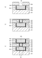
12 ビットライン
14 ONO膜
16 BPSG膜
18 キャップ層
20 マスク層
22 コンタクトホール
24 バリア層
26 コンタクトプラグ
28 窒化膜
30 第1絶縁膜
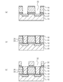
32 溝部
34 バリア層
36 Cuシード層
38 Cu膜
40 Cu配線
42 酸化膜
44 Cuシリサイド層
46 第2絶縁膜
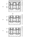
50 半導体基板
52a 第1酸化膜
52b 第2酸化膜
52c 第3酸化膜
54a 第1溝部
54b 第2溝部
56 バリア層
58 Cuシード層
60 Cu膜
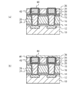
62a 第1配線層
62b 第2配線層
64a 第1窒化膜
64b 第2窒化膜
64c 第3窒化膜
66 ビア
68 ビア孔
70 ボイド
Claims (10)
- 半導体基板上に形成された絶縁膜に溝部を形成する工程と、
前記溝部に埋め込まれるように、前記絶縁膜上に金属膜を形成する工程と、
前記絶縁膜上に形成された前記金属膜を平坦化し、前記溝部に前記金属膜からなる配線層を形成する工程と、
前記配線層の表面に形成された酸化膜を除去するため、前記配線層の表面にプラズマ処理を行う工程と、
前記プラズマ処理を行う工程の後、前記半導体基板を大気に曝すことなく、シラン系ガスを含むガス雰囲気中で、前記半導体基板に熱処理を行う工程と、を有することを特徴とする半導体装置の製造方法。 - 前記プラズマ処理を行う工程は、前記半導体基板をアンモニアガス雰囲気中、水素ガス雰囲気中、及びヒドラジンガス雰囲気中のいずれかの雰囲気中に曝して、前記配線層の表面にプラズマ処理を行う工程であることを特徴とする請求項1記載の半導体装置の製造方法。
- 前記熱処理を行う工程は、モノシランガスまたはジシランガスを含むガス雰囲気中で、前記半導体基板に熱処理を行う工程であることを特徴とする請求項1または2記載の半導体装置の製造方法。
- 前記プラズマ処理を行う工程は、前記半導体基板をアンモニアガス雰囲気中に曝して、前記配線層の表面にプラズマ処理を行う工程であり、
前記熱処理を行う工程は、前記アンモニアガス雰囲気中にモノシランガスを導入し、前記アンモニアガスと前記モノシランガスとの混合ガス雰囲気中で、前記半導体基板に熱処理を行う工程であることを特徴とする請求項1記載の半導体装置の製造方法。 - 前記熱処理を行う工程は、前記半導体基板に0.5秒から2秒の前記熱処理を行う工程であることを特徴とする請求項1から4のいずれか一項記載の半導体装置の製造方法。
- 前記金属膜の結晶性を向上させるため、前記金属膜にアニールを行う工程を有し、
前記金属膜にアニールを行う工程は、前記熱処理を行う工程の前に実施することを特徴とする請求項1から5のいずれか一項記載の半導体装置の製造方法。 - 前記熱処理を行う工程は、前記配線層の表面が活性化された状態で、前記熱処理を行う工程であることを特徴とする請求項1から6のいずれか一項記載の半導体装置の製造方法。
- 前記配線層は銅配線であることを特徴とする請求項1から7のいずれか一項記載の半導体装置の製造方法。
- 半導体基板上に設けられた溝部を有する絶縁膜と、
前記溝部に埋め込まれるように設けられた配線層と、
前記配線層の表面に形成されたシリサイド層と、を具備し、
前記配線層と前記シリサイド層との間には、酸化膜が介在していないことを特徴とする半導体装置。 - 前記配線層は銅配線であることを特徴とする請求項9記載の半導体装置。
Priority Applications (1)
| Application Number | Priority Date | Filing Date | Title |
|---|---|---|---|
| JP2008167045A JP5595644B2 (ja) | 2008-06-26 | 2008-06-26 | 半導体装置及びその製造方法 |
Applications Claiming Priority (1)
| Application Number | Priority Date | Filing Date | Title |
|---|---|---|---|
| JP2008167045A JP5595644B2 (ja) | 2008-06-26 | 2008-06-26 | 半導体装置及びその製造方法 |
Publications (2)
| Publication Number | Publication Date |
|---|---|
| JP2010010338A true JP2010010338A (ja) | 2010-01-14 |
| JP5595644B2 JP5595644B2 (ja) | 2014-09-24 |
Family
ID=41590486
Family Applications (1)
| Application Number | Title | Priority Date | Filing Date |
|---|---|---|---|
| JP2008167045A Expired - Fee Related JP5595644B2 (ja) | 2008-06-26 | 2008-06-26 | 半導体装置及びその製造方法 |
Country Status (1)
| Country | Link |
|---|---|
| JP (1) | JP5595644B2 (ja) |
Cited By (1)
| Publication number | Priority date | Publication date | Assignee | Title |
|---|---|---|---|---|
| JP2014507065A (ja) * | 2010-12-22 | 2014-03-20 | アプライド マテリアルズ インコーポレイテッド | シリコンウエハのシリコン貫通ビアの製造 |
Citations (4)
| Publication number | Priority date | Publication date | Assignee | Title |
|---|---|---|---|---|
| JP2002246391A (ja) * | 2001-02-21 | 2002-08-30 | Nec Corp | 半導体装置の製造方法 |
| JP2004096052A (ja) * | 2002-03-13 | 2004-03-25 | Nec Electronics Corp | 半導体装置およびその製造方法ならびに金属配線 |
| JP2004342977A (ja) * | 2003-05-19 | 2004-12-02 | Nec Electronics Corp | 半導体装置の製造方法 |
| JP2005340460A (ja) * | 2004-05-26 | 2005-12-08 | Renesas Technology Corp | 半導体装置の形成方法 |
-
2008
- 2008-06-26 JP JP2008167045A patent/JP5595644B2/ja not_active Expired - Fee Related
Patent Citations (4)
| Publication number | Priority date | Publication date | Assignee | Title |
|---|---|---|---|---|
| JP2002246391A (ja) * | 2001-02-21 | 2002-08-30 | Nec Corp | 半導体装置の製造方法 |
| JP2004096052A (ja) * | 2002-03-13 | 2004-03-25 | Nec Electronics Corp | 半導体装置およびその製造方法ならびに金属配線 |
| JP2004342977A (ja) * | 2003-05-19 | 2004-12-02 | Nec Electronics Corp | 半導体装置の製造方法 |
| JP2005340460A (ja) * | 2004-05-26 | 2005-12-08 | Renesas Technology Corp | 半導体装置の形成方法 |
Cited By (1)
| Publication number | Priority date | Publication date | Assignee | Title |
|---|---|---|---|---|
| JP2014507065A (ja) * | 2010-12-22 | 2014-03-20 | アプライド マテリアルズ インコーポレイテッド | シリコンウエハのシリコン貫通ビアの製造 |
Also Published As
| Publication number | Publication date |
|---|---|
| JP5595644B2 (ja) | 2014-09-24 |
Similar Documents
| Publication | Publication Date | Title |
|---|---|---|
| US9899258B1 (en) | Metal liner overhang reduction and manufacturing method thereof | |
| US11315830B2 (en) | Metallic interconnect structures with wrap around capping layers | |
| JP4647184B2 (ja) | 半導体装置の製造方法 | |
| KR20130085351A (ko) | 구리 배선들을 갖는 반도체 디바이스들 및 그 제조 방법들 | |
| US20120244698A1 (en) | Methods for forming copper diffusion barriers for semiconductor interconnect structures | |
| TWI762064B (zh) | 半導體裝置結構及其製造方法 | |
| JP5141761B2 (ja) | 半導体装置及びその製造方法 | |
| US12400962B2 (en) | Liner-free conductive structures with anchor points | |
| US7199043B2 (en) | Method of forming copper wiring in semiconductor device | |
| US12532719B2 (en) | Barrier schemes for metallization using manganese and graphene | |
| US6881661B2 (en) | Manufacturing method of semiconductor device | |
| JP2000252278A (ja) | 半導体装置およびその製造方法 | |
| JP2008147675A (ja) | 不均一窒化金属膜を用いる電気的接続構造物の形成方法およびこの方法によって製造された接続構造物 | |
| JP5217272B2 (ja) | 配線の形成方法及び半導体装置の製造方法 | |
| JP5595644B2 (ja) | 半導体装置及びその製造方法 | |
| JP4492919B2 (ja) | 半導体装置の製造方法 | |
| JP2010153487A (ja) | 半導体装置及びその製造方法 | |
| JP4173393B2 (ja) | 半導体装置の製造方法 | |
| JP4457884B2 (ja) | 半導体装置 | |
| JP2015133382A (ja) | 半導体装置の製造方法 | |
| US20120068343A1 (en) | Semiconductor device and method for manufacturing the same | |
| JP2005191512A (ja) | 半導体装置の製造方法 | |
| JP5917603B2 (ja) | 半導体装置およびその製造方法 | |
| US7989342B2 (en) | Formation of a reliable diffusion-barrier cap on a Cu-containing interconnect element having grains with different crystal orientations | |
| JP2006319116A (ja) | 半導体装置およびその製造方法 |
Legal Events
| Date | Code | Title | Description |
|---|---|---|---|
| RD04 | Notification of resignation of power of attorney |
Free format text: JAPANESE INTERMEDIATE CODE: A7424 Effective date: 20100402 |
|
| RD03 | Notification of appointment of power of attorney |
Free format text: JAPANESE INTERMEDIATE CODE: A7423 Effective date: 20100616 |
|
| A621 | Written request for application examination |
Free format text: JAPANESE INTERMEDIATE CODE: A621 Effective date: 20110621 |
|
| A521 | Request for written amendment filed |
Free format text: JAPANESE INTERMEDIATE CODE: A523 Effective date: 20110819 |
|
| RD03 | Notification of appointment of power of attorney |
Free format text: JAPANESE INTERMEDIATE CODE: A7423 Effective date: 20120830 |
|
| A977 | Report on retrieval |
Free format text: JAPANESE INTERMEDIATE CODE: A971007 Effective date: 20130415 |
|
| A131 | Notification of reasons for refusal |
Free format text: JAPANESE INTERMEDIATE CODE: A131 Effective date: 20130418 |
|
| A601 | Written request for extension of time |
Free format text: JAPANESE INTERMEDIATE CODE: A601 Effective date: 20130717 |
|
| A602 | Written permission of extension of time |
Free format text: JAPANESE INTERMEDIATE CODE: A602 Effective date: 20130722 |
|
| A521 | Request for written amendment filed |
Free format text: JAPANESE INTERMEDIATE CODE: A523 Effective date: 20130819 |
|
| A131 | Notification of reasons for refusal |
Free format text: JAPANESE INTERMEDIATE CODE: A131 Effective date: 20130904 |
|
| A601 | Written request for extension of time |
Free format text: JAPANESE INTERMEDIATE CODE: A601 Effective date: 20131203 |
|
| A602 | Written permission of extension of time |
Free format text: JAPANESE INTERMEDIATE CODE: A602 Effective date: 20131206 |
|
| A601 | Written request for extension of time |
Free format text: JAPANESE INTERMEDIATE CODE: A601 Effective date: 20131226 |
|
| A602 | Written permission of extension of time |
Free format text: JAPANESE INTERMEDIATE CODE: A602 Effective date: 20140107 |
|
| A601 | Written request for extension of time |
Free format text: JAPANESE INTERMEDIATE CODE: A601 Effective date: 20140203 |
|
| A602 | Written permission of extension of time |
Free format text: JAPANESE INTERMEDIATE CODE: A602 Effective date: 20140206 |
|
| A521 | Request for written amendment filed |
Free format text: JAPANESE INTERMEDIATE CODE: A523 Effective date: 20140214 |
|
| TRDD | Decision of grant or rejection written | ||
| A01 | Written decision to grant a patent or to grant a registration (utility model) |
Free format text: JAPANESE INTERMEDIATE CODE: A01 Effective date: 20140708 |
|
| A61 | First payment of annual fees (during grant procedure) |
Free format text: JAPANESE INTERMEDIATE CODE: A61 Effective date: 20140806 |
|
| R150 | Certificate of patent or registration of utility model |
Ref document number: 5595644 Country of ref document: JP Free format text: JAPANESE INTERMEDIATE CODE: R150 |
|
| S111 | Request for change of ownership or part of ownership |
Free format text: JAPANESE INTERMEDIATE CODE: R313111 |
|
| R350 | Written notification of registration of transfer |
Free format text: JAPANESE INTERMEDIATE CODE: R350 |
|
| R250 | Receipt of annual fees |
Free format text: JAPANESE INTERMEDIATE CODE: R250 |
|
| R250 | Receipt of annual fees |
Free format text: JAPANESE INTERMEDIATE CODE: R250 |
|
| R250 | Receipt of annual fees |
Free format text: JAPANESE INTERMEDIATE CODE: R250 |
|
| R250 | Receipt of annual fees |
Free format text: JAPANESE INTERMEDIATE CODE: R250 |
|
| R250 | Receipt of annual fees |
Free format text: JAPANESE INTERMEDIATE CODE: R250 |
|
| R250 | Receipt of annual fees |
Free format text: JAPANESE INTERMEDIATE CODE: R250 |
|
| LAPS | Cancellation because of no payment of annual fees |