JP2009147263A - 配線基板およびその製造方法 - Google Patents
配線基板およびその製造方法 Download PDFInfo
- Publication number
- JP2009147263A JP2009147263A JP2007325747A JP2007325747A JP2009147263A JP 2009147263 A JP2009147263 A JP 2009147263A JP 2007325747 A JP2007325747 A JP 2007325747A JP 2007325747 A JP2007325747 A JP 2007325747A JP 2009147263 A JP2009147263 A JP 2009147263A
- Authority
- JP
- Japan
- Prior art keywords
- wiring board
- wiring
- layer
- conductor portion
- substrate
- Prior art date
- Legal status (The legal status is an assumption and is not a legal conclusion. Google has not performed a legal analysis and makes no representation as to the accuracy of the status listed.)
- Pending
Links
Images

Classifications
-
- H—ELECTRICITY
- H05—ELECTRIC TECHNIQUES NOT OTHERWISE PROVIDED FOR
- H05K—PRINTED CIRCUITS; CASINGS OR CONSTRUCTIONAL DETAILS OF ELECTRIC APPARATUS; MANUFACTURE OF ASSEMBLAGES OF ELECTRICAL COMPONENTS
- H05K1/00—Printed circuits
- H05K1/02—Details
- H05K1/0271—Arrangements for reducing stress or warp in rigid printed circuit boards, e.g. caused by loads, vibrations or differences in thermal expansion
-
- H—ELECTRICITY
- H05—ELECTRIC TECHNIQUES NOT OTHERWISE PROVIDED FOR
- H05K—PRINTED CIRCUITS; CASINGS OR CONSTRUCTIONAL DETAILS OF ELECTRIC APPARATUS; MANUFACTURE OF ASSEMBLAGES OF ELECTRICAL COMPONENTS
- H05K3/00—Apparatus or processes for manufacturing printed circuits
- H05K3/46—Manufacturing multilayer circuits
- H05K3/4602—Manufacturing multilayer circuits characterized by a special circuit board as base or central core whereon additional circuit layers are built or additional circuit boards are laminated
-
- H—ELECTRICITY
- H05—ELECTRIC TECHNIQUES NOT OTHERWISE PROVIDED FOR
- H05K—PRINTED CIRCUITS; CASINGS OR CONSTRUCTIONAL DETAILS OF ELECTRIC APPARATUS; MANUFACTURE OF ASSEMBLAGES OF ELECTRICAL COMPONENTS
- H05K2201/00—Indexing scheme relating to printed circuits covered by H05K1/00
- H05K2201/09—Shape and layout
- H05K2201/09209—Shape and layout details of conductors
- H05K2201/095—Conductive through-holes or vias
- H05K2201/09563—Metal filled via
-
- H—ELECTRICITY
- H05—ELECTRIC TECHNIQUES NOT OTHERWISE PROVIDED FOR
- H05K—PRINTED CIRCUITS; CASINGS OR CONSTRUCTIONAL DETAILS OF ELECTRIC APPARATUS; MANUFACTURE OF ASSEMBLAGES OF ELECTRICAL COMPONENTS
- H05K2201/00—Indexing scheme relating to printed circuits covered by H05K1/00
- H05K2201/09—Shape and layout
- H05K2201/09209—Shape and layout details of conductors
- H05K2201/09654—Shape and layout details of conductors covering at least two types of conductors provided for in H05K2201/09218 - H05K2201/095
- H05K2201/09681—Mesh conductors, e.g. as a ground plane
-
- H—ELECTRICITY
- H05—ELECTRIC TECHNIQUES NOT OTHERWISE PROVIDED FOR
- H05K—PRINTED CIRCUITS; CASINGS OR CONSTRUCTIONAL DETAILS OF ELECTRIC APPARATUS; MANUFACTURE OF ASSEMBLAGES OF ELECTRICAL COMPONENTS
- H05K2201/00—Indexing scheme relating to printed circuits covered by H05K1/00
- H05K2201/09—Shape and layout
- H05K2201/09209—Shape and layout details of conductors
- H05K2201/09654—Shape and layout details of conductors covering at least two types of conductors provided for in H05K2201/09218 - H05K2201/095
- H05K2201/09781—Dummy conductors, i.e. not used for normal transport of current; Dummy electrodes of components
-
- H—ELECTRICITY
- H05—ELECTRIC TECHNIQUES NOT OTHERWISE PROVIDED FOR
- H05K—PRINTED CIRCUITS; CASINGS OR CONSTRUCTIONAL DETAILS OF ELECTRIC APPARATUS; MANUFACTURE OF ASSEMBLAGES OF ELECTRICAL COMPONENTS
- H05K3/00—Apparatus or processes for manufacturing printed circuits
- H05K3/40—Forming printed elements for providing electric connections to or between printed circuits
- H05K3/42—Plated through-holes or plated via connections
Landscapes
- Engineering & Computer Science (AREA)
- Microelectronics & Electronic Packaging (AREA)
- Manufacturing & Machinery (AREA)
- Production Of Multi-Layered Print Wiring Board (AREA)
Priority Applications (3)
| Application Number | Priority Date | Filing Date | Title |
|---|---|---|---|
| JP2007325747A JP2009147263A (ja) | 2007-12-18 | 2007-12-18 | 配線基板およびその製造方法 |
| US12/335,907 US20090166077A1 (en) | 2007-12-18 | 2008-12-16 | Wiring board and method of manufacturing the same |
| TW097149133A TW200938012A (en) | 2007-12-18 | 2008-12-17 | Wiring board and method of manufacturing the same |
Applications Claiming Priority (1)
| Application Number | Priority Date | Filing Date | Title |
|---|---|---|---|
| JP2007325747A JP2009147263A (ja) | 2007-12-18 | 2007-12-18 | 配線基板およびその製造方法 |
Publications (2)
| Publication Number | Publication Date |
|---|---|
| JP2009147263A true JP2009147263A (ja) | 2009-07-02 |
| JP2009147263A5 JP2009147263A5 (enExample) | 2010-10-21 |
Family
ID=40796730
Family Applications (1)
| Application Number | Title | Priority Date | Filing Date |
|---|---|---|---|
| JP2007325747A Pending JP2009147263A (ja) | 2007-12-18 | 2007-12-18 | 配線基板およびその製造方法 |
Country Status (3)
| Country | Link |
|---|---|
| US (1) | US20090166077A1 (enExample) |
| JP (1) | JP2009147263A (enExample) |
| TW (1) | TW200938012A (enExample) |
Cited By (1)
| Publication number | Priority date | Publication date | Assignee | Title |
|---|---|---|---|---|
| JP2015107598A (ja) * | 2013-12-05 | 2015-06-11 | Jx日鉱日石金属株式会社 | 樹脂基板を互いに剥離可能に密着させた積層体 |
Families Citing this family (6)
| Publication number | Priority date | Publication date | Assignee | Title |
|---|---|---|---|---|
| US8921705B2 (en) * | 2008-11-28 | 2014-12-30 | Ibiden Co., Ltd. | Wiring board and fabrication method therefor |
| US20100139967A1 (en) * | 2008-12-08 | 2010-06-10 | Ibiden Co., Ltd. | Wiring board and fabrication method therefor |
| TW201110839A (en) * | 2009-09-04 | 2011-03-16 | Advanced Semiconductor Eng | Substrate structure and method for manufacturing the same |
| JP2013214568A (ja) * | 2012-03-30 | 2013-10-17 | Fujitsu Ltd | 配線基板及び配線基板の製造方法 |
| KR101548816B1 (ko) * | 2013-11-11 | 2015-08-31 | 삼성전기주식회사 | 인쇄회로기판 및 그 제조방법 |
| KR102436226B1 (ko) * | 2015-08-19 | 2022-08-25 | 삼성전기주식회사 | 인쇄회로기판 및 그 제조방법 |
Citations (3)
| Publication number | Priority date | Publication date | Assignee | Title |
|---|---|---|---|---|
| JPH04279097A (ja) * | 1991-03-07 | 1992-10-05 | Sony Corp | プリント配線板の放熱構造 |
| JP2003347727A (ja) * | 2002-05-30 | 2003-12-05 | Hitachi Ltd | 配線基板および両面実装半導体製品 |
| WO2007052674A1 (ja) * | 2005-11-02 | 2007-05-10 | Ibiden Co., Ltd. | 半導体装置用多層プリント配線板及びその製造方法 |
Family Cites Families (3)
| Publication number | Priority date | Publication date | Assignee | Title |
|---|---|---|---|---|
| JPH07109943B2 (ja) * | 1992-12-09 | 1995-11-22 | 日本電気株式会社 | 多層配線基板 |
| DE4334127C1 (de) * | 1993-10-07 | 1995-03-23 | Mtu Muenchen Gmbh | Metallkernleiterplatte zum Einschieben in das Gehäuse eines Elektronikgerätes |
| US7714453B2 (en) * | 2006-05-12 | 2010-05-11 | Broadcom Corporation | Interconnect structure and formation for package stacking of molded plastic area array package |
-
2007
- 2007-12-18 JP JP2007325747A patent/JP2009147263A/ja active Pending
-
2008
- 2008-12-16 US US12/335,907 patent/US20090166077A1/en not_active Abandoned
- 2008-12-17 TW TW097149133A patent/TW200938012A/zh unknown
Patent Citations (3)
| Publication number | Priority date | Publication date | Assignee | Title |
|---|---|---|---|---|
| JPH04279097A (ja) * | 1991-03-07 | 1992-10-05 | Sony Corp | プリント配線板の放熱構造 |
| JP2003347727A (ja) * | 2002-05-30 | 2003-12-05 | Hitachi Ltd | 配線基板および両面実装半導体製品 |
| WO2007052674A1 (ja) * | 2005-11-02 | 2007-05-10 | Ibiden Co., Ltd. | 半導体装置用多層プリント配線板及びその製造方法 |
Cited By (1)
| Publication number | Priority date | Publication date | Assignee | Title |
|---|---|---|---|---|
| JP2015107598A (ja) * | 2013-12-05 | 2015-06-11 | Jx日鉱日石金属株式会社 | 樹脂基板を互いに剥離可能に密着させた積層体 |
Also Published As
| Publication number | Publication date |
|---|---|
| US20090166077A1 (en) | 2009-07-02 |
| TW200938012A (en) | 2009-09-01 |
Similar Documents
| Publication | Publication Date | Title |
|---|---|---|
| JP5122594B2 (ja) | 凹凸パターン付きビアパッドを含む印刷回路基板 | |
| CN103416110B (zh) | 印刷电路板及其制造方法 | |
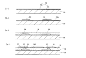
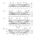
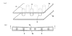
| JP2009147263A (ja) | 配線基板およびその製造方法 | |
| CN103179784A (zh) | 具有一体化法拉第屏蔽的多层电子结构 | |
| US20140116759A1 (en) | Printed wiring board and method for manufacturing printed wiring board | |
| JP2015170770A (ja) | プリント配線板 | |
| KR101332079B1 (ko) | 다층 인쇄회로기판 제조 방법 및 이에 따라 제조된 다층 인쇄회로기판 | |
| JP2013540368A (ja) | 印刷回路基板及びその製造方法 | |
| US7363706B2 (en) | Method of manufacturing a multilayer printed wiring board | |
| JP2009147263A5 (enExample) | ||
| KR101987378B1 (ko) | 인쇄회로기판의 제조 방법 | |
| JP2017084914A (ja) | 印刷配線板およびその製造方法 | |
| JP5791078B2 (ja) | 配線基板 | |
| KR102436226B1 (ko) | 인쇄회로기판 및 그 제조방법 | |
| JP4964322B2 (ja) | 放熱基板およびその製造方法 | |
| JP2017005168A (ja) | プリント配線板およびその製造方法 | |
| JP2020057767A (ja) | プリント配線基板 | |
| JP2016127248A (ja) | 多層配線基板 | |
| JP5621311B2 (ja) | 回路基板の製造方法 | |
| KR20150003505A (ko) | 인쇄회로기판 및 이의 제조방법 | |
| JP7187821B2 (ja) | プリント配線板およびその製造方法 | |
| JP6417765B2 (ja) | 配線基板用の積層体、これを用いた配線基板及びその製造方法 | |
| JP4227967B2 (ja) | 基板及び電子部品の製造方法 | |
| KR102812877B1 (ko) | 회로 기판 | |
| JP2005072064A (ja) | 配線基板およびその製造方法 |
Legal Events
| Date | Code | Title | Description |
|---|---|---|---|
| A521 | Request for written amendment filed |
Free format text: JAPANESE INTERMEDIATE CODE: A523 Effective date: 20100906 |
|
| A621 | Written request for application examination |
Free format text: JAPANESE INTERMEDIATE CODE: A621 Effective date: 20100906 |
|
| A977 | Report on retrieval |
Free format text: JAPANESE INTERMEDIATE CODE: A971007 Effective date: 20120130 |
|
| A131 | Notification of reasons for refusal |
Free format text: JAPANESE INTERMEDIATE CODE: A131 Effective date: 20120207 |
|
| A02 | Decision of refusal |
Free format text: JAPANESE INTERMEDIATE CODE: A02 Effective date: 20120612 |