JP2007294514A - 半導体装置 - Google Patents
半導体装置 Download PDFInfo
- Publication number
- JP2007294514A JP2007294514A JP2006117720A JP2006117720A JP2007294514A JP 2007294514 A JP2007294514 A JP 2007294514A JP 2006117720 A JP2006117720 A JP 2006117720A JP 2006117720 A JP2006117720 A JP 2006117720A JP 2007294514 A JP2007294514 A JP 2007294514A
- Authority
- JP
- Japan
- Prior art keywords
- insulating film
- lower electrode
- interlayer insulating
- film
- diameter
- Prior art date
- Legal status (The legal status is an assumption and is not a legal conclusion. Google has not performed a legal analysis and makes no representation as to the accuracy of the status listed.)
- Pending
Links
Images


Classifications
-
- H—ELECTRICITY
- H01—ELECTRIC ELEMENTS
- H01L—SEMICONDUCTOR DEVICES NOT COVERED BY CLASS H10
- H01L23/00—Details of semiconductor or other solid state devices
- H01L23/52—Arrangements for conducting electric current within the device in operation from one component to another, i.e. interconnections, e.g. wires, lead frames
- H01L23/522—Arrangements for conducting electric current within the device in operation from one component to another, i.e. interconnections, e.g. wires, lead frames including external interconnections consisting of a multilayer structure of conductive and insulating layers inseparably formed on the semiconductor body
- H01L23/5222—Capacitive arrangements or effects of, or between wiring layers
- H01L23/5223—Capacitor integral with wiring layers
-
- H—ELECTRICITY
- H01—ELECTRIC ELEMENTS
- H01L—SEMICONDUCTOR DEVICES NOT COVERED BY CLASS H10
- H01L21/00—Processes or apparatus adapted for the manufacture or treatment of semiconductor or solid state devices or of parts thereof
- H01L21/70—Manufacture or treatment of devices consisting of a plurality of solid state components formed in or on a common substrate or of parts thereof; Manufacture of integrated circuit devices or of parts thereof
- H01L21/71—Manufacture of specific parts of devices defined in group H01L21/70
- H01L21/768—Applying interconnections to be used for carrying current between separate components within a device comprising conductors and dielectrics
- H01L21/76801—Applying interconnections to be used for carrying current between separate components within a device comprising conductors and dielectrics characterised by the formation and the after-treatment of the dielectrics, e.g. smoothing
- H01L21/76802—Applying interconnections to be used for carrying current between separate components within a device comprising conductors and dielectrics characterised by the formation and the after-treatment of the dielectrics, e.g. smoothing by forming openings in dielectrics
- H01L21/76816—Aspects relating to the layout of the pattern or to the size of vias or trenches
-
- H—ELECTRICITY
- H01—ELECTRIC ELEMENTS
- H01L—SEMICONDUCTOR DEVICES NOT COVERED BY CLASS H10
- H01L21/00—Processes or apparatus adapted for the manufacture or treatment of semiconductor or solid state devices or of parts thereof
- H01L21/70—Manufacture or treatment of devices consisting of a plurality of solid state components formed in or on a common substrate or of parts thereof; Manufacture of integrated circuit devices or of parts thereof
- H01L21/71—Manufacture of specific parts of devices defined in group H01L21/70
- H01L21/768—Applying interconnections to be used for carrying current between separate components within a device comprising conductors and dielectrics
- H01L21/76838—Applying interconnections to be used for carrying current between separate components within a device comprising conductors and dielectrics characterised by the formation and the after-treatment of the conductors
- H01L21/7684—Smoothing; Planarisation
-
- H—ELECTRICITY
- H01—ELECTRIC ELEMENTS
- H01L—SEMICONDUCTOR DEVICES NOT COVERED BY CLASS H10
- H01L28/00—Passive two-terminal components without a potential-jump or surface barrier for integrated circuits; Details thereof; Multistep manufacturing processes therefor
- H01L28/40—Capacitors
- H01L28/60—Electrodes
-
- H—ELECTRICITY
- H01—ELECTRIC ELEMENTS
- H01L—SEMICONDUCTOR DEVICES NOT COVERED BY CLASS H10
- H01L23/00—Details of semiconductor or other solid state devices
- H01L23/52—Arrangements for conducting electric current within the device in operation from one component to another, i.e. interconnections, e.g. wires, lead frames
- H01L23/522—Arrangements for conducting electric current within the device in operation from one component to another, i.e. interconnections, e.g. wires, lead frames including external interconnections consisting of a multilayer structure of conductive and insulating layers inseparably formed on the semiconductor body
- H01L23/532—Arrangements for conducting electric current within the device in operation from one component to another, i.e. interconnections, e.g. wires, lead frames including external interconnections consisting of a multilayer structure of conductive and insulating layers inseparably formed on the semiconductor body characterised by the materials
- H01L23/53204—Conductive materials
- H01L23/53209—Conductive materials based on metals, e.g. alloys, metal silicides
- H01L23/53228—Conductive materials based on metals, e.g. alloys, metal silicides the principal metal being copper
- H01L23/53238—Additional layers associated with copper layers, e.g. adhesion, barrier, cladding layers
-
- H—ELECTRICITY
- H01—ELECTRIC ELEMENTS
- H01L—SEMICONDUCTOR DEVICES NOT COVERED BY CLASS H10
- H01L23/00—Details of semiconductor or other solid state devices
- H01L23/52—Arrangements for conducting electric current within the device in operation from one component to another, i.e. interconnections, e.g. wires, lead frames
- H01L23/522—Arrangements for conducting electric current within the device in operation from one component to another, i.e. interconnections, e.g. wires, lead frames including external interconnections consisting of a multilayer structure of conductive and insulating layers inseparably formed on the semiconductor body
- H01L23/532—Arrangements for conducting electric current within the device in operation from one component to another, i.e. interconnections, e.g. wires, lead frames including external interconnections consisting of a multilayer structure of conductive and insulating layers inseparably formed on the semiconductor body characterised by the materials
- H01L23/5329—Insulating materials
- H01L23/53295—Stacked insulating layers
-
- H—ELECTRICITY
- H01—ELECTRIC ELEMENTS
- H01L—SEMICONDUCTOR DEVICES NOT COVERED BY CLASS H10
- H01L2924/00—Indexing scheme for arrangements or methods for connecting or disconnecting semiconductor or solid-state bodies as covered by H01L24/00
- H01L2924/0001—Technical content checked by a classifier
- H01L2924/0002—Not covered by any one of groups H01L24/00, H01L24/00 and H01L2224/00
Abstract
【解決手段】電極溝11c上にビアホール開口用の開口部OP1を、また、キャパシタ形成領域外に設けられた配線層9bの上方部に対応する位置の層間絶縁膜6上に配線層9bとの接続のためのビアホール開口用の開口部OP2を形成する。このとき、開口部OP1の開口直径は、開口部OP2よりも大きく設定するものとし、例えば開口部OP2の直径が0.36μmであるならば、開口部OP1の開口直径は0.38μmに設定する。
【選択図】図5
Description
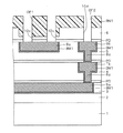
本発明に係る実施の形態の説明に先立って、MIM構造のキャパシタに発生するディッシングについて説明する。
まず発明者達は、下部電極が完全に除去される部分が発生するのを防止するには、下部電極の厚みを増せば良いという技術思想を得た。しかし、発明者達の採用する下部電極の製造方法は、デュアルダマシンの中でも電極形成用の電極溝を最初に形成するトレンチファーストという手法であり、この場合、最初に深い溝を形成すると、次に、ビア(via)ホールを形成する際にフォトリソグラフィによりレジストを感光するときのフォーカス位置が、深くなってしまうが、フォトリソグラフィ装置の焦点深度(DOF)の調整範囲(フォーカスマージン)にも制限があり、電極用の溝を深くするとビアホールの直径が設計通りに形成できず、下層配線とのコンタクトが確実にできないという問題があった。
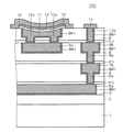
まず、製造工程を順に示す断面図である図3〜図9を用いて本発明に係る半導体装置100の製造方法について説明する。なお、半導体装置100の構成については最終工程を示す図9に示す。なお、半導体装置100においては図1に示した半導体装置90と同一の構成には同一の符号を付し、重複する説明は省略する。
ここで、図4を用いて説明したように、電極溝11cの深さを約350nmとして図1に示した半導体装置90よりも深くしたが、フォトリソグラフィ装置の焦点深度(DOF)の調整範囲の制限は問題とならなかった。
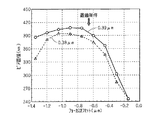
図10においては、横軸にフォーカスオフセット(μm)を縦軸にビアホールの直径(nm)を示し、0.38μmのビアホールを形成する場合と、0.39μmのビアホールを形成する場合について、フォーカスオフセットを変化させた場合にビアホール直径がどのように変化するかについて示している。なお、図10においてはDOFが深くなる方向をマイナス方向として示している。
以上説明した本発明に係る実施の形態1の半導体装置においては、下部電極11と下層配線とを電気的に接続するコンタクトプラグ10aの直径を他の部分のコンタクトプラグよりも大きくすることで、DOFマージンを大きくして、CMP時の下部電極11の過研磨に対する耐性を高める構成を示したが、下部電極の過研磨を低減することで耐圧不良を起こすキャパシタの発生を防止するようにしても良い。
Claims (2)
- 半導体基板の上方に配設された層間絶縁膜と
前記層間絶縁膜の上層部に配設された下部電極と、
前記下部電極上に配設された誘電体膜と、
前記誘電体膜を間に挟んで前記下部電極に対向して配設された上部電極とを有したキャパシタを備え、前記下部電極は、その底部から前記半導体基板の主面に垂直な方向に前記層間絶縁膜を貫通するように設けられたコンタクトプラグと一体をなす半導体装置であって、
前記コンタクトプラグの直径は、前記層間絶縁膜を前記半導体基板の主面と垂直な方向に貫通するように設けられた他のコンタクトプラグの直径よりも広く形成される、半導体装置。 - 前記コンタクトプラグの直径は、前記他のコンタクトプラグの直径の1.05倍以上である、請求項1記載の半導体装置。
Priority Applications (2)
| Application Number | Priority Date | Filing Date | Title |
|---|---|---|---|
| JP2006117720A JP2007294514A (ja) | 2006-04-21 | 2006-04-21 | 半導体装置 |
| US11/733,975 US20070246799A1 (en) | 2006-04-21 | 2007-04-11 | Semiconductor device |
Applications Claiming Priority (1)
| Application Number | Priority Date | Filing Date | Title |
|---|---|---|---|
| JP2006117720A JP2007294514A (ja) | 2006-04-21 | 2006-04-21 | 半導体装置 |
Publications (2)
| Publication Number | Publication Date |
|---|---|
| JP2007294514A true JP2007294514A (ja) | 2007-11-08 |
| JP2007294514A5 JP2007294514A5 (ja) | 2009-05-14 |
Family
ID=38618698
Family Applications (1)
| Application Number | Title | Priority Date | Filing Date |
|---|---|---|---|
| JP2006117720A Pending JP2007294514A (ja) | 2006-04-21 | 2006-04-21 | 半導体装置 |
Country Status (2)
| Country | Link |
|---|---|
| US (1) | US20070246799A1 (ja) |
| JP (1) | JP2007294514A (ja) |
Families Citing this family (2)
| Publication number | Priority date | Publication date | Assignee | Title |
|---|---|---|---|---|
| JP2008300676A (ja) * | 2007-05-31 | 2008-12-11 | Rohm Co Ltd | 半導体装置およびその製造方法 |
| CN114203442B (zh) * | 2021-12-03 | 2023-11-03 | 灿芯半导体(上海)股份有限公司 | 一种用于高精度电容阵列的电容单元 |
Citations (3)
| Publication number | Priority date | Publication date | Assignee | Title |
|---|---|---|---|---|
| JPH061349A (ja) * | 1992-06-12 | 1994-01-11 | Kawasaki Steel Corp | 溶接缶胴を有する缶体 |
| JP2000164812A (ja) * | 1998-11-27 | 2000-06-16 | Sharp Corp | 半導体装置及びその製造方法 |
| JP2004022694A (ja) * | 2002-06-14 | 2004-01-22 | Renesas Technology Corp | 半導体装置の製造方法 |
Family Cites Families (5)
| Publication number | Priority date | Publication date | Assignee | Title |
|---|---|---|---|---|
| US6504205B1 (en) * | 2001-06-15 | 2003-01-07 | Silicon Integrated Systems Corp. | Metal capacitors with damascene structures |
| JP4076131B2 (ja) * | 2002-06-07 | 2008-04-16 | 富士通株式会社 | 半導体装置の製造方法 |
| JP2004079924A (ja) * | 2002-08-22 | 2004-03-11 | Renesas Technology Corp | 半導体装置 |
| US6867447B2 (en) * | 2003-05-20 | 2005-03-15 | Texas Instruments Incorporated | Ferroelectric memory cell and methods for fabricating the same |
| US6876028B1 (en) * | 2003-09-30 | 2005-04-05 | International Business Machines Corporation | Metal-insulator-metal capacitor and method of fabrication |
-
2006
- 2006-04-21 JP JP2006117720A patent/JP2007294514A/ja active Pending
-
2007
- 2007-04-11 US US11/733,975 patent/US20070246799A1/en not_active Abandoned
Patent Citations (3)
| Publication number | Priority date | Publication date | Assignee | Title |
|---|---|---|---|---|
| JPH061349A (ja) * | 1992-06-12 | 1994-01-11 | Kawasaki Steel Corp | 溶接缶胴を有する缶体 |
| JP2000164812A (ja) * | 1998-11-27 | 2000-06-16 | Sharp Corp | 半導体装置及びその製造方法 |
| JP2004022694A (ja) * | 2002-06-14 | 2004-01-22 | Renesas Technology Corp | 半導体装置の製造方法 |
Also Published As
| Publication number | Publication date |
|---|---|
| US20070246799A1 (en) | 2007-10-25 |
Similar Documents
| Publication | Publication Date | Title |
|---|---|---|
| JP3961412B2 (ja) | 半導体装置及びその形成方法 | |
| US20050263848A1 (en) | Metal-insulator-metal capacitor having a large capacitance and method of manufacturing the same | |
| JP2007221161A (ja) | 半導体デバイスで用いられるキャパシタとその製造方法 | |
| JP2006191036A (ja) | 半導体素子及びその形成方法 | |
| US6849920B2 (en) | Semiconductor capacitive element, method for manufacturing same and semiconductor device provided with same | |
| JP2005142369A (ja) | 半導体装置の製造方法 | |
| JP2007049089A (ja) | 半導体装置およびその製造方法 | |
| JP4848137B2 (ja) | 半導体装置およびその製造方法 | |
| US20090149019A1 (en) | Semiconductor device and method for fabricating the same | |
| JP4272168B2 (ja) | 半導体装置及び半導体集積回路装置 | |
| JP5613272B2 (ja) | 半導体装置 | |
| JP5388478B2 (ja) | 半導体装置 | |
| JP2007294514A (ja) | 半導体装置 | |
| JP2006228977A (ja) | 半導体装置及び半導体装置の製造方法 | |
| US7005343B2 (en) | Semiconductor device and method of manufacturing the same | |
| JP2004079924A (ja) | 半導体装置 | |
| JP2008124070A (ja) | 半導体装置 | |
| JP4211910B2 (ja) | 半導体装置の製造方法 | |
| JP5424551B2 (ja) | 半導体装置 | |
| JP2008294403A (ja) | 半導体装置 | |
| KR20070013894A (ko) | 반도체 소자의 금속 배선 형성 방법 | |
| KR20090055772A (ko) | 반도체 소자의 금속 배선 형성 방법 | |
| JP2008171886A (ja) | 半導体装置およびその製造方法 | |
| JP2008098424A (ja) | 半導体装置および半導体装置の製造方法 | |
| WO2011030476A1 (ja) | 半導体装置の製造方法 |
Legal Events
| Date | Code | Title | Description |
|---|---|---|---|
| A521 | Written amendment |
Free format text: JAPANESE INTERMEDIATE CODE: A523 Effective date: 20090326 |
|
| A621 | Written request for application examination |
Free format text: JAPANESE INTERMEDIATE CODE: A621 Effective date: 20090326 |
|
| RD04 | Notification of resignation of power of attorney |
Free format text: JAPANESE INTERMEDIATE CODE: A7424 Effective date: 20090326 |
|
| A711 | Notification of change in applicant |
Free format text: JAPANESE INTERMEDIATE CODE: A712 Effective date: 20100524 |
|
| A131 | Notification of reasons for refusal |
Free format text: JAPANESE INTERMEDIATE CODE: A131 Effective date: 20120501 |
|
| A977 | Report on retrieval |
Free format text: JAPANESE INTERMEDIATE CODE: A971007 Effective date: 20120502 |
|
| A02 | Decision of refusal |
Free format text: JAPANESE INTERMEDIATE CODE: A02 Effective date: 20120904 |