JP2007165902A - 透過型集積型薄膜太陽電池及びその製造方法と、その単位セルを電気的に直列接続する方法 - Google Patents
透過型集積型薄膜太陽電池及びその製造方法と、その単位セルを電気的に直列接続する方法 Download PDFInfo
- Publication number
- JP2007165902A JP2007165902A JP2006335615A JP2006335615A JP2007165902A JP 2007165902 A JP2007165902 A JP 2007165902A JP 2006335615 A JP2006335615 A JP 2006335615A JP 2006335615 A JP2006335615 A JP 2006335615A JP 2007165902 A JP2007165902 A JP 2007165902A
- Authority
- JP
- Japan
- Prior art keywords
- conductive material
- solar cell
- layer
- thin film
- film solar
- Prior art date
- Legal status (The legal status is an assumption and is not a legal conclusion. Google has not performed a legal analysis and makes no representation as to the accuracy of the status listed.)
- Granted
Links
- 238000000034 method Methods 0.000 title claims abstract description 225
- 239000010409 thin film Substances 0.000 title claims abstract description 114
- 238000004519 manufacturing process Methods 0.000 title claims abstract description 25
- 239000000758 substrate Substances 0.000 claims abstract description 69
- 238000005530 etching Methods 0.000 claims abstract description 55
- 238000000151 deposition Methods 0.000 claims abstract description 34
- 239000004065 semiconductor Substances 0.000 claims abstract description 30
- 239000004020 conductor Substances 0.000 claims description 359
- 230000005540 biological transmission Effects 0.000 claims description 43
- 238000007639 printing Methods 0.000 claims description 39
- 238000003980 solgel method Methods 0.000 claims description 6
- 239000000126 substance Substances 0.000 abstract description 16
- 238000000059 patterning Methods 0.000 description 49
- 229920002120 photoresistant polymer Polymers 0.000 description 32
- 229920000642 polymer Polymers 0.000 description 28
- XLOMVQKBTHCTTD-UHFFFAOYSA-N Zinc monoxide Chemical compound [Zn]=O XLOMVQKBTHCTTD-UHFFFAOYSA-N 0.000 description 25
- 230000008021 deposition Effects 0.000 description 19
- 229910021417 amorphous silicon Inorganic materials 0.000 description 18
- 239000011787 zinc oxide Substances 0.000 description 12
- XUIMIQQOPSSXEZ-UHFFFAOYSA-N Silicon Chemical compound [Si] XUIMIQQOPSSXEZ-UHFFFAOYSA-N 0.000 description 11
- 238000010894 electron beam technology Methods 0.000 description 11
- 239000010408 film Substances 0.000 description 11
- AMGQUBHHOARCQH-UHFFFAOYSA-N indium;oxotin Chemical compound [In].[Sn]=O AMGQUBHHOARCQH-UHFFFAOYSA-N 0.000 description 11
- 229910052751 metal Inorganic materials 0.000 description 11
- 239000002184 metal Substances 0.000 description 11
- 229910052710 silicon Inorganic materials 0.000 description 11
- 239000010703 silicon Substances 0.000 description 11
- XOLBLPGZBRYERU-UHFFFAOYSA-N tin dioxide Chemical compound O=[Sn]=O XOLBLPGZBRYERU-UHFFFAOYSA-N 0.000 description 11
- 229910001887 tin oxide Inorganic materials 0.000 description 11
- 238000009413 insulation Methods 0.000 description 10
- 238000003672 processing method Methods 0.000 description 10
- 238000002207 thermal evaporation Methods 0.000 description 10
- PXHVJJICTQNCMI-UHFFFAOYSA-N Nickel Chemical compound [Ni] PXHVJJICTQNCMI-UHFFFAOYSA-N 0.000 description 9
- 238000009834 vaporization Methods 0.000 description 8
- 238000010586 diagram Methods 0.000 description 7
- 238000000206 photolithography Methods 0.000 description 7
- 238000007650 screen-printing Methods 0.000 description 7
- 230000008016 vaporization Effects 0.000 description 7
- 239000011651 chromium Substances 0.000 description 6
- 239000010949 copper Substances 0.000 description 6
- 238000005520 cutting process Methods 0.000 description 6
- 238000005566 electron beam evaporation Methods 0.000 description 6
- 238000001704 evaporation Methods 0.000 description 6
- 239000010931 gold Substances 0.000 description 6
- 230000004048 modification Effects 0.000 description 6
- 238000012986 modification Methods 0.000 description 6
- 239000002994 raw material Substances 0.000 description 6
- 239000010936 titanium Substances 0.000 description 6
- 238000007740 vapor deposition Methods 0.000 description 6
- 229910000577 Silicon-germanium Inorganic materials 0.000 description 5
- 238000006243 chemical reaction Methods 0.000 description 5
- 238000001020 plasma etching Methods 0.000 description 5
- 230000015572 biosynthetic process Effects 0.000 description 4
- 238000001312 dry etching Methods 0.000 description 4
- 238000007646 gravure printing Methods 0.000 description 4
- 239000000463 material Substances 0.000 description 4
- VYZAMTAEIAYCRO-UHFFFAOYSA-N Chromium Chemical compound [Cr] VYZAMTAEIAYCRO-UHFFFAOYSA-N 0.000 description 3
- RYGMFSIKBFXOCR-UHFFFAOYSA-N Copper Chemical compound [Cu] RYGMFSIKBFXOCR-UHFFFAOYSA-N 0.000 description 3
- BQCADISMDOOEFD-UHFFFAOYSA-N Silver Chemical compound [Ag] BQCADISMDOOEFD-UHFFFAOYSA-N 0.000 description 3
- RTAQQCXQSZGOHL-UHFFFAOYSA-N Titanium Chemical compound [Ti] RTAQQCXQSZGOHL-UHFFFAOYSA-N 0.000 description 3
- LEVVHYCKPQWKOP-UHFFFAOYSA-N [Si].[Ge] Chemical compound [Si].[Ge] LEVVHYCKPQWKOP-UHFFFAOYSA-N 0.000 description 3
- 229910052782 aluminium Inorganic materials 0.000 description 3
- XAGFODPZIPBFFR-UHFFFAOYSA-N aluminium Chemical compound [Al] XAGFODPZIPBFFR-UHFFFAOYSA-N 0.000 description 3
- 229910052804 chromium Inorganic materials 0.000 description 3
- 150000001875 compounds Chemical class 0.000 description 3
- 229910052802 copper Inorganic materials 0.000 description 3
- PCHJSUWPFVWCPO-UHFFFAOYSA-N gold Chemical compound [Au] PCHJSUWPFVWCPO-UHFFFAOYSA-N 0.000 description 3
- 229910052737 gold Inorganic materials 0.000 description 3
- 239000007769 metal material Substances 0.000 description 3
- 229910052759 nickel Inorganic materials 0.000 description 3
- 229910052709 silver Inorganic materials 0.000 description 3
- 239000004332 silver Substances 0.000 description 3
- 229910052719 titanium Inorganic materials 0.000 description 3
- WFKWXMTUELFFGS-UHFFFAOYSA-N tungsten Chemical compound [W] WFKWXMTUELFFGS-UHFFFAOYSA-N 0.000 description 3
- 229910052721 tungsten Inorganic materials 0.000 description 3
- 239000010937 tungsten Substances 0.000 description 3
- JBRZTFJDHDCESZ-UHFFFAOYSA-N AsGa Chemical compound [As]#[Ga] JBRZTFJDHDCESZ-UHFFFAOYSA-N 0.000 description 2
- 229910001218 Gallium arsenide Inorganic materials 0.000 description 2
- GPXJNWSHGFTCBW-UHFFFAOYSA-N Indium phosphide Chemical compound [In]#P GPXJNWSHGFTCBW-UHFFFAOYSA-N 0.000 description 2
- ZOKXTWBITQBERF-UHFFFAOYSA-N Molybdenum Chemical compound [Mo] ZOKXTWBITQBERF-UHFFFAOYSA-N 0.000 description 2
- 229910006404 SnO 2 Inorganic materials 0.000 description 2
- 230000015556 catabolic process Effects 0.000 description 2
- 238000006731 degradation reaction Methods 0.000 description 2
- 230000000694 effects Effects 0.000 description 2
- 229910052750 molybdenum Inorganic materials 0.000 description 2
- 239000011733 molybdenum Substances 0.000 description 2
- 229910021421 monocrystalline silicon Inorganic materials 0.000 description 2
- 229910021420 polycrystalline silicon Inorganic materials 0.000 description 2
- MARUHZGHZWCEQU-UHFFFAOYSA-N 5-phenyl-2h-tetrazole Chemical compound C1=CC=CC=C1C1=NNN=N1 MARUHZGHZWCEQU-UHFFFAOYSA-N 0.000 description 1
- 229910004613 CdTe Inorganic materials 0.000 description 1
- KTSFMFGEAAANTF-UHFFFAOYSA-N [Cu].[Se].[Se].[In] Chemical compound [Cu].[Se].[Se].[In] KTSFMFGEAAANTF-UHFFFAOYSA-N 0.000 description 1
- 239000011149 active material Substances 0.000 description 1
- 239000002131 composite material Substances 0.000 description 1
- 239000000356 contaminant Substances 0.000 description 1
- 238000011109 contamination Methods 0.000 description 1
- 238000010924 continuous production Methods 0.000 description 1
- 230000005611 electricity Effects 0.000 description 1
- 238000005516 engineering process Methods 0.000 description 1
- 239000011521 glass Substances 0.000 description 1
- 239000012212 insulator Substances 0.000 description 1
- 238000003754 machining Methods 0.000 description 1
- 229910021424 microcrystalline silicon Inorganic materials 0.000 description 1
- 238000001259 photo etching Methods 0.000 description 1
- 229920003023 plastic Polymers 0.000 description 1
- 238000010248 power generation Methods 0.000 description 1
- 230000002265 prevention Effects 0.000 description 1
- 230000001681 protective effect Effects 0.000 description 1
- 230000007261 regionalization Effects 0.000 description 1
- 239000011347 resin Substances 0.000 description 1
- 229920005989 resin Polymers 0.000 description 1
- 238000004544 sputter deposition Methods 0.000 description 1
Images


Classifications
-
- B—PERFORMING OPERATIONS; TRANSPORTING
- B29—WORKING OF PLASTICS; WORKING OF SUBSTANCES IN A PLASTIC STATE IN GENERAL
- B29D—PRODUCING PARTICULAR ARTICLES FROM PLASTICS OR FROM SUBSTANCES IN A PLASTIC STATE
- B29D11/00—Producing optical elements, e.g. lenses or prisms
-
- H—ELECTRICITY
- H01—ELECTRIC ELEMENTS
- H01L—SEMICONDUCTOR DEVICES NOT COVERED BY CLASS H10
- H01L31/00—Semiconductor devices sensitive to infrared radiation, light, electromagnetic radiation of shorter wavelength or corpuscular radiation and specially adapted either for the conversion of the energy of such radiation into electrical energy or for the control of electrical energy by such radiation; Processes or apparatus specially adapted for the manufacture or treatment thereof or of parts thereof; Details thereof
- H01L31/04—Semiconductor devices sensitive to infrared radiation, light, electromagnetic radiation of shorter wavelength or corpuscular radiation and specially adapted either for the conversion of the energy of such radiation into electrical energy or for the control of electrical energy by such radiation; Processes or apparatus specially adapted for the manufacture or treatment thereof or of parts thereof; Details thereof adapted as photovoltaic [PV] conversion devices
- H01L31/042—PV modules or arrays of single PV cells
- H01L31/0445—PV modules or arrays of single PV cells including thin film solar cells, e.g. single thin film a-Si, CIS or CdTe solar cells
- H01L31/046—PV modules composed of a plurality of thin film solar cells deposited on the same substrate
-
- H—ELECTRICITY
- H01—ELECTRIC ELEMENTS
- H01L—SEMICONDUCTOR DEVICES NOT COVERED BY CLASS H10
- H01L31/00—Semiconductor devices sensitive to infrared radiation, light, electromagnetic radiation of shorter wavelength or corpuscular radiation and specially adapted either for the conversion of the energy of such radiation into electrical energy or for the control of electrical energy by such radiation; Processes or apparatus specially adapted for the manufacture or treatment thereof or of parts thereof; Details thereof
- H01L31/04—Semiconductor devices sensitive to infrared radiation, light, electromagnetic radiation of shorter wavelength or corpuscular radiation and specially adapted either for the conversion of the energy of such radiation into electrical energy or for the control of electrical energy by such radiation; Processes or apparatus specially adapted for the manufacture or treatment thereof or of parts thereof; Details thereof adapted as photovoltaic [PV] conversion devices
-
- H—ELECTRICITY
- H01—ELECTRIC ELEMENTS
- H01L—SEMICONDUCTOR DEVICES NOT COVERED BY CLASS H10
- H01L31/00—Semiconductor devices sensitive to infrared radiation, light, electromagnetic radiation of shorter wavelength or corpuscular radiation and specially adapted either for the conversion of the energy of such radiation into electrical energy or for the control of electrical energy by such radiation; Processes or apparatus specially adapted for the manufacture or treatment thereof or of parts thereof; Details thereof
- H01L31/02—Details
- H01L31/0216—Coatings
-
- H—ELECTRICITY
- H01—ELECTRIC ELEMENTS
- H01L—SEMICONDUCTOR DEVICES NOT COVERED BY CLASS H10
- H01L31/00—Semiconductor devices sensitive to infrared radiation, light, electromagnetic radiation of shorter wavelength or corpuscular radiation and specially adapted either for the conversion of the energy of such radiation into electrical energy or for the control of electrical energy by such radiation; Processes or apparatus specially adapted for the manufacture or treatment thereof or of parts thereof; Details thereof
- H01L31/04—Semiconductor devices sensitive to infrared radiation, light, electromagnetic radiation of shorter wavelength or corpuscular radiation and specially adapted either for the conversion of the energy of such radiation into electrical energy or for the control of electrical energy by such radiation; Processes or apparatus specially adapted for the manufacture or treatment thereof or of parts thereof; Details thereof adapted as photovoltaic [PV] conversion devices
- H01L31/042—PV modules or arrays of single PV cells
- H01L31/0445—PV modules or arrays of single PV cells including thin film solar cells, e.g. single thin film a-Si, CIS or CdTe solar cells
- H01L31/046—PV modules composed of a plurality of thin film solar cells deposited on the same substrate
- H01L31/0463—PV modules composed of a plurality of thin film solar cells deposited on the same substrate characterised by special patterning methods to connect the PV cells in a module, e.g. laser cutting of the conductive or active layers
-
- H—ELECTRICITY
- H01—ELECTRIC ELEMENTS
- H01L—SEMICONDUCTOR DEVICES NOT COVERED BY CLASS H10
- H01L31/00—Semiconductor devices sensitive to infrared radiation, light, electromagnetic radiation of shorter wavelength or corpuscular radiation and specially adapted either for the conversion of the energy of such radiation into electrical energy or for the control of electrical energy by such radiation; Processes or apparatus specially adapted for the manufacture or treatment thereof or of parts thereof; Details thereof
- H01L31/04—Semiconductor devices sensitive to infrared radiation, light, electromagnetic radiation of shorter wavelength or corpuscular radiation and specially adapted either for the conversion of the energy of such radiation into electrical energy or for the control of electrical energy by such radiation; Processes or apparatus specially adapted for the manufacture or treatment thereof or of parts thereof; Details thereof adapted as photovoltaic [PV] conversion devices
- H01L31/042—PV modules or arrays of single PV cells
- H01L31/0445—PV modules or arrays of single PV cells including thin film solar cells, e.g. single thin film a-Si, CIS or CdTe solar cells
- H01L31/046—PV modules composed of a plurality of thin film solar cells deposited on the same substrate
- H01L31/0465—PV modules composed of a plurality of thin film solar cells deposited on the same substrate comprising particular structures for the electrical interconnection of adjacent PV cells in the module
-
- H—ELECTRICITY
- H01—ELECTRIC ELEMENTS
- H01L—SEMICONDUCTOR DEVICES NOT COVERED BY CLASS H10
- H01L31/00—Semiconductor devices sensitive to infrared radiation, light, electromagnetic radiation of shorter wavelength or corpuscular radiation and specially adapted either for the conversion of the energy of such radiation into electrical energy or for the control of electrical energy by such radiation; Processes or apparatus specially adapted for the manufacture or treatment thereof or of parts thereof; Details thereof
- H01L31/04—Semiconductor devices sensitive to infrared radiation, light, electromagnetic radiation of shorter wavelength or corpuscular radiation and specially adapted either for the conversion of the energy of such radiation into electrical energy or for the control of electrical energy by such radiation; Processes or apparatus specially adapted for the manufacture or treatment thereof or of parts thereof; Details thereof adapted as photovoltaic [PV] conversion devices
- H01L31/042—PV modules or arrays of single PV cells
- H01L31/0445—PV modules or arrays of single PV cells including thin film solar cells, e.g. single thin film a-Si, CIS or CdTe solar cells
- H01L31/046—PV modules composed of a plurality of thin film solar cells deposited on the same substrate
- H01L31/0468—PV modules composed of a plurality of thin film solar cells deposited on the same substrate comprising specific means for obtaining partial light transmission through the module, e.g. partially transparent thin film solar modules for windows
-
- H—ELECTRICITY
- H01—ELECTRIC ELEMENTS
- H01L—SEMICONDUCTOR DEVICES NOT COVERED BY CLASS H10
- H01L31/00—Semiconductor devices sensitive to infrared radiation, light, electromagnetic radiation of shorter wavelength or corpuscular radiation and specially adapted either for the conversion of the energy of such radiation into electrical energy or for the control of electrical energy by such radiation; Processes or apparatus specially adapted for the manufacture or treatment thereof or of parts thereof; Details thereof
- H01L31/18—Processes or apparatus specially adapted for the manufacture or treatment of these devices or of parts thereof
- H01L31/1876—Particular processes or apparatus for batch treatment of the devices
- H01L31/188—Apparatus specially adapted for automatic interconnection of solar cells in a module
-
- H—ELECTRICITY
- H01—ELECTRIC ELEMENTS
- H01L—SEMICONDUCTOR DEVICES NOT COVERED BY CLASS H10
- H01L31/00—Semiconductor devices sensitive to infrared radiation, light, electromagnetic radiation of shorter wavelength or corpuscular radiation and specially adapted either for the conversion of the energy of such radiation into electrical energy or for the control of electrical energy by such radiation; Processes or apparatus specially adapted for the manufacture or treatment thereof or of parts thereof; Details thereof
- H01L31/18—Processes or apparatus specially adapted for the manufacture or treatment of these devices or of parts thereof
- H01L31/20—Processes or apparatus specially adapted for the manufacture or treatment of these devices or of parts thereof such devices or parts thereof comprising amorphous semiconductor materials
- H01L31/202—Processes or apparatus specially adapted for the manufacture or treatment of these devices or of parts thereof such devices or parts thereof comprising amorphous semiconductor materials including only elements of Group IV of the Periodic System
-
- Y—GENERAL TAGGING OF NEW TECHNOLOGICAL DEVELOPMENTS; GENERAL TAGGING OF CROSS-SECTIONAL TECHNOLOGIES SPANNING OVER SEVERAL SECTIONS OF THE IPC; TECHNICAL SUBJECTS COVERED BY FORMER USPC CROSS-REFERENCE ART COLLECTIONS [XRACs] AND DIGESTS
- Y02—TECHNOLOGIES OR APPLICATIONS FOR MITIGATION OR ADAPTATION AGAINST CLIMATE CHANGE
- Y02E—REDUCTION OF GREENHOUSE GAS [GHG] EMISSIONS, RELATED TO ENERGY GENERATION, TRANSMISSION OR DISTRIBUTION
- Y02E10/00—Energy generation through renewable energy sources
- Y02E10/50—Photovoltaic [PV] energy
-
- Y—GENERAL TAGGING OF NEW TECHNOLOGICAL DEVELOPMENTS; GENERAL TAGGING OF CROSS-SECTIONAL TECHNOLOGIES SPANNING OVER SEVERAL SECTIONS OF THE IPC; TECHNICAL SUBJECTS COVERED BY FORMER USPC CROSS-REFERENCE ART COLLECTIONS [XRACs] AND DIGESTS
- Y02—TECHNOLOGIES OR APPLICATIONS FOR MITIGATION OR ADAPTATION AGAINST CLIMATE CHANGE
- Y02P—CLIMATE CHANGE MITIGATION TECHNOLOGIES IN THE PRODUCTION OR PROCESSING OF GOODS
- Y02P70/00—Climate change mitigation technologies in the production process for final industrial or consumer products
- Y02P70/50—Manufacturing or production processes characterised by the final manufactured product
Abstract
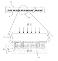
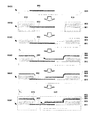
【解決手段】本発明に係る透過型集積型薄膜太陽電池の製造方法は、透明基板上に帯状のパターンで離隔し、光が前記透明基板を直接通過し得る所定の空間を含むように、第1導電性物質を形成するステップ(a)と、太陽電池(半導体)層を形成するステップ(b)と、第2導電性物質を斜めに蒸着するステップ(c)と、前記第2導電性物質層をマスクとして、前記太陽電池層をエッチングするステップ(d)と、を含む。
【選択図】図3
Description
本発明の利点及び特徴、そしてそれらを達成する方法は、添付する図面と共に詳細に後述されている実施形態を参照すると、明確になるはずである。明細書全体にわたって同一の構成要素には同一の参照符号を付してある。
Claims (18)
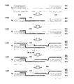
- 透明基板上に帯状のパターンで離隔し、光が前記透明基板を直接通過し得る所定の空間を含むように、第1導電性物質を形成するステップ(a)と、
太陽電池(半導体)層を形成するステップ(b)と、
第2導電性物質を斜めに蒸着するステップ(c)と、
前記第2導電性物質層をマスクとして、前記太陽電池層をエッチングするステップ(d)と
を含む、透過型集積型薄膜太陽電池の製造方法。 - 前記ステップ(a)の前記第1導電性物質層が、前記透過型集積型薄膜太陽電池の単位セルの境界面に所定の間隔分伸びて形成される、請求項1に記載の透過型集積型薄膜太陽電池の製造方法。
- 前記ステップ(a)の前記所定の空間が6角形状である、請求項1に記載の透過型集積型薄膜太陽電池の製造方法。
- 透明基板上に帯状のパターンで離隔し、光が前記透明基板を直接通過し得る所定の空間を含むように、第1導電性物質を形成するステップ(a)と、
太陽電池(半導体)層を形成するステップ(b)と、
第2導電性物質を斜めに蒸着するステップ(c)と、
前記第2導電性物質層をマスクとして、前記太陽電池層をエッチングするステップ(d)と
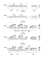
を含む、透過型集積型薄膜太陽電池の製造方法により形成された、透過型集積型薄膜太陽電池。 - 2ケ以上の透過型集積型薄膜太陽電池の単位セルを電気的に直列接続する方法であって、
透明基板上に帯状にパターニングされた第1導電性物質層を形成するステップ(a)と、
離隔するようにパターニングされ、隣接したパターンのうちの何れかのパターンと前記第1導電性物質層の一部とが電気的に接続されるように、第2導電性物質層を形成するステップ(b)と、
太陽電池(半導体)層を形成するステップ(c)と、
第3導電性物質を斜めに蒸着するステップ(d)と、
前記第3導電性物質層をマスクとして、前記太陽電池層をエッチングするステップ(e)と、
前記第1導電性物質層と前記第3導電性物質層とを電気的に接続するように、第4導電性物質を形成するステップ(f)と
を含む、透過型集積型薄膜太陽電池の単位セルを電気的に直列接続する方法。 - 前記第2導電性物質が透明な導電性物質である、請求項5に記載の透過型集積型薄膜太陽電池の単位セルを電気的に直列接続する方法。
- 前記ステップ(b)において、前記第1導電性物質層上に前記パターニングされた第2導電性物質と離隔するように、前記第2導電性物質のダミーパターンがさらに形成される、請求項5に記載の透過型集積型薄膜太陽電池の単位セルを電気的に直列接続する方法。
- 2ケ以上の透過型集積型薄膜太陽電池の単位セルを電気的に直列接続する方法であって
透明基板上に相互間に離隔するように帯状にパターニングされた第1導電性物質層を形成するステップ(a)と、
離隔するようにパターニングされ、隣接したパターンのうちの何れかのパターンと前記第1導電性物質層の一部とが電気的に接続されるように第2導電性物質層を形成するステップ(b)と、
太陽電池(半導体)層を形成するステップ(c)と、
第3導電性物質を斜めに蒸着するステップ(d)と、
前記第3導電性物質層をマスクとして、前記太陽電池層をエッチングするステップ(e)と、
前記第2導電性物質層と前記第3導電性物質層とを電気的に接続するように、第4導電性物質を形成するステップ(f)と
を含む、透過型集積型薄膜太陽電池の単位セルを電気的に直列接続する方法 。 - 前記第1導電性物質が、透明な導電性物質である、請求項8に記載の透過型集積型薄膜太陽電池の単位セルを電気的に直列接続する方法 。
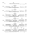
- 2ケ以上の透過型集積型薄膜太陽電池の単位セルを電気的に直列接続する方法であって、
透明基板上に離隔するように帯状にパターニングされた第1導電性物質層を形成するステップ(a)と、
太陽電池(半導体)層を形成するステップ(b)と、
第2導電性物質を斜めに蒸着するステップ(c)と、
前記第2導電性物質層をマスクとして、前記太陽電池層をエッチングするステップ(d)と、
前記第1導電性物質層と前記第2導電性物質層とを電気的に接続するように、第3導電性物質を形成するステップ(e)と
を含む、透過型集積型薄膜太陽電池の単位セルを電気的に直列接続する方法。 - 前記第1導電性物質が透明な導電性物質である、請求項10に記載の透過型集積型薄膜太陽電池の単位セルを電気的に直列接続する方法。
- 前記ステップ(a)にいいてパターニングされた第1導電性物質層の一部が、段差があるように形成される、請求項10に記載の透過型集積型薄膜太陽電池の単位セルを電気的に直列接続する方法。
- 前記段差が、陽刻、陰刻のうちの何れかの形態である、請求項12に記載の透過型集積型薄膜太陽電池の単位セルを電気的に直列接続する方法。
- 前記段差が、ゾルゲル(sol−gel)法、ナノインプリント(nano−imprint)または印刷法(printing)のうちの何れかの方法により形成される、請求項12に記載の透過型集積型薄膜太陽電池の単位セルを電気的に直列接続する方法。
- 2ケ以上の透過型集積型薄膜太陽電池の単位セルを電気的に直列接続する方法であって、
透明基板上に離隔するように帯状にパターニングされた第1導電性物質層を形成するステップ(a)と、
離隔するようにパターニングされ、隣接したパターンのうちの何れかのパターンと前記第1導電性物質層の一部とが電気的に接続されるように第2導電性物質層を形成するステップ(b)と、
太陽電池(半導体)層を形成するステップ(c)と、
第3導電性物質を斜めに蒸着するステップ(d)と、
第4導電性物質を斜めに蒸着するステップ(e)と、
前記第3導電性物質及び第4導電性物質をマスクとして、前記太陽電池層をエッチングするステップ(f)と、
前記第1導電性物質と前記第3導電性物質とを電気的に接続するように、第5導電性物質を形成するステップ(g)と
を含む、透過型集積型薄膜太陽電池の単位セルを電気的に直列接続する方法。 - 前記第2導電性物質が透明な導電性物質である、請求項15に記載の透過型集積型薄膜太陽電池の単位セルを電気的に直列接続する方法 製造方法。
- 2ケ以上の透過型集積型薄膜太陽電池の単位セルを電気的に直列接続する方法であって、
透明基板上に離隔するように帯状にパターニングされた第1導電性物質層を形成するステップ(a)と、
離隔するようにパターニングされ、隣接したパターンのうちの何れかのパターンと前記第1導電性物質層の一部とが電気的に接続されるように第2導電性物質層を形成するステップ(b)と、
太陽電池(半導体)層を形成するステップ(c)と、
第3導電性物質を斜めに蒸着するステップ(d)と、
前記第3導電性物質層をマスクとして、前記太陽電池層をエッチングするステップ(e)と、
前記第1導電性物質と前記第3導電性物質とを電気的に接続するように、第4導電性物質を斜めに蒸着するステップ(f)と
を含む、透過型集積型薄膜太陽電池の単位セルを電気的に直列接続する方法。 - 前記第2導電性物質が透明な導電性物質である、請求項17に記載の透過型集積型薄膜太陽電池の単位セルを電気的に直列接続する方法。
Applications Claiming Priority (1)
| Application Number | Priority Date | Filing Date | Title |
|---|---|---|---|
| KR1020050123355A KR100725110B1 (ko) | 2005-12-14 | 2005-12-14 | 투과형 집적형 박막 태양전지 및 그 제조 방법. |
Publications (2)
| Publication Number | Publication Date |
|---|---|
| JP2007165902A true JP2007165902A (ja) | 2007-06-28 |
| JP4592676B2 JP4592676B2 (ja) | 2010-12-01 |
Family
ID=37909613
Family Applications (1)
| Application Number | Title | Priority Date | Filing Date |
|---|---|---|---|
| JP2006335615A Expired - Fee Related JP4592676B2 (ja) | 2005-12-14 | 2006-12-13 | 透過型集積型薄膜太陽電池の製造方法及び透過型集積型薄膜太陽電池の単位セルを電気的に直列接続する方法 |
Country Status (5)
| Country | Link |
|---|---|
| US (1) | US8449782B2 (ja) |
| EP (1) | EP1798779A3 (ja) |
| JP (1) | JP4592676B2 (ja) |
| KR (1) | KR100725110B1 (ja) |
| CN (1) | CN100536118C (ja) |
Cited By (6)
| Publication number | Priority date | Publication date | Assignee | Title |
|---|---|---|---|---|
| WO2010123196A1 (en) * | 2009-04-24 | 2010-10-28 | Jusung Engineering Co., Ltd. | Thin film type solar cell, and method for manufacturing the same |
| JP2010278441A (ja) * | 2009-05-26 | 2010-12-09 | Korea Iron & Steel Co Ltd | 集積型薄膜太陽電池及びその製造方法 |
| JP2011040746A (ja) * | 2009-08-06 | 2011-02-24 | Korea Iron & Steel Co Ltd | 光起電力装置及びその製造方法 |
| US8298852B2 (en) | 2008-12-29 | 2012-10-30 | Jusung Engineering Co., Ltd. | Thin film type solar cell and method for manufacturing the same |
| JP2016519442A (ja) * | 2013-05-23 | 2016-06-30 | サンパートナー テクノロジーズSunpartner Technologies | 半透明薄層光起電力モノセル |
| JP2017076720A (ja) * | 2015-10-15 | 2017-04-20 | 国立研究開発法人産業技術総合研究所 | 熱電変換モジュールの作製方法 |
Families Citing this family (19)
| Publication number | Priority date | Publication date | Assignee | Title |
|---|---|---|---|---|
| WO2006107154A1 (en) * | 2005-03-16 | 2006-10-12 | Korea Advanced Institute Of Science And Technology | Integrated thin-film solar cells and method of manufacturing thereof and processing method of transparent electrode for integrated thin-film solar cells and structure thereof, and transparent substrate having processed transparent electrode |
| KR100725110B1 (ko) | 2005-12-14 | 2007-06-04 | 한국과학기술원 | 투과형 집적형 박막 태양전지 및 그 제조 방법. |
| KR100656738B1 (ko) * | 2005-12-14 | 2006-12-14 | 한국과학기술원 | 집적형 박막 태양전지 및 그 제조 방법 |
| CN102124273B (zh) | 2008-06-18 | 2013-05-29 | 乐信股份公司 | 用于显示烹饪物料选择或烹饪程序选择的方法和为此的烹饪器具 |
| CN101958361A (zh) * | 2009-07-13 | 2011-01-26 | 无锡尚德太阳能电力有限公司 | 透光薄膜太阳电池组件刻蚀方法 |
| TWI397189B (zh) * | 2009-12-24 | 2013-05-21 | Au Optronics Corp | 製作太陽能薄膜電池之方法及其結構 |
| WO2011097430A2 (en) * | 2010-02-05 | 2011-08-11 | E. I. Du Pont De Nemours And Company | Masking pastes and processes for manufacturing a partially transparent thin-film photovoltaic panel |
| US9214583B2 (en) * | 2010-03-19 | 2015-12-15 | Hirak Mitra | Method to build transparent polarizing solar cell |
| US8563351B2 (en) * | 2010-06-25 | 2013-10-22 | Taiwan Semiconductor Manufacturing Co., Ltd. | Method for manufacturing photovoltaic device |
| KR101060239B1 (ko) * | 2010-08-26 | 2011-08-29 | 한국과학기술원 | 집적형 박막 광기전력 소자 및 그의 제조 방법 |
| KR101173380B1 (ko) | 2010-10-07 | 2012-08-10 | 엘지이노텍 주식회사 | 태양광 발전장치 및 이의 제조방법 |
| US8834664B2 (en) | 2010-10-22 | 2014-09-16 | Guardian Industries Corp. | Photovoltaic modules for use in vehicle roofs, and/or methods of making the same |
| CN102615371B (zh) * | 2012-03-31 | 2014-03-26 | 宁夏小牛自动化设备有限公司 | 太阳能电池串焊设备及防烟雾结晶的太阳能电池串焊焊头 |
| WO2013158581A1 (en) * | 2012-04-18 | 2013-10-24 | Guardian Industries Corp. | Improved photovoltaic modules for use in vehicle roofs, and/or methods of making the same |
| US9647158B2 (en) * | 2013-05-21 | 2017-05-09 | Alliance For Sustainable Energy, Llc | Photovoltaic sub-cell interconnects |
| JP5787112B2 (ja) * | 2013-11-08 | 2015-09-30 | トヨタ自動車株式会社 | 車両の太陽電池搭載構造 |
| KR20150078549A (ko) | 2013-12-31 | 2015-07-08 | 한국과학기술원 | 집적형 박막 태양전지의 제조 장치 |
| DE102015211392B4 (de) * | 2015-06-19 | 2018-05-24 | Albert-Ludwigs-Universität Freiburg | Elektrodenstruktur und Verfahren zum Herstellen der Elektrodenstruktur und Biosensor-Chip die Elektrodenstruktur umfassend |
| KR102253547B1 (ko) * | 2018-11-29 | 2021-05-18 | 울산과학기술원 | 무색 투명 반도체 기판 및 이의 제조방법 |
Citations (8)
| Publication number | Priority date | Publication date | Assignee | Title |
|---|---|---|---|---|
| JPS5712568A (en) * | 1980-06-02 | 1982-01-22 | Rca Corp | Method of producing solar battery |
| JPS6135573A (ja) * | 1984-07-27 | 1986-02-20 | Matsushita Electric Ind Co Ltd | 光起電力素子の製造法 |
| JPS62142368A (ja) * | 1985-12-17 | 1987-06-25 | Fuji Electric Co Ltd | 薄膜半導体装置の製造方法 |
| JPS6342180A (ja) * | 1986-08-08 | 1988-02-23 | Toa Nenryo Kogyo Kk | 集積型光起電力装置の製造方法 |
| JPH05258859A (ja) * | 1991-12-30 | 1993-10-08 | Eastman Kodak Co | 発光装置及びその製造方法 |
| JP2003101053A (ja) * | 2001-09-27 | 2003-04-04 | Sanyo Electric Co Ltd | 太陽電池装置及びその製造方法 |
| JP2005101384A (ja) * | 2003-09-26 | 2005-04-14 | Sanyo Electric Co Ltd | 光起電力装置及びその製造方法 |
| JP2005197537A (ja) * | 2004-01-09 | 2005-07-21 | Matsushita Electric Ind Co Ltd | 集積型薄膜太陽電池およびその製造方法 |
Family Cites Families (38)
| Publication number | Priority date | Publication date | Assignee | Title |
|---|---|---|---|---|
| US3994012A (en) * | 1975-05-07 | 1976-11-23 | The Regents Of The University Of Minnesota | Photovoltaic semi-conductor devices |
| US4200472A (en) * | 1978-06-05 | 1980-04-29 | The Regents Of The University Of California | Solar power system and high efficiency photovoltaic cells used therein |
| US4514582A (en) * | 1982-09-17 | 1985-04-30 | Exxon Research And Engineering Co. | Optical absorption enhancement in amorphous silicon deposited on rough substrate |
| US4501636A (en) * | 1983-12-28 | 1985-02-26 | The United States Of America As Represented By The Secretary Of The Air Force | Apparatus for etching vertical junction solar cell wafers |
| JPS60182757A (ja) * | 1984-02-29 | 1985-09-18 | Kanegafuchi Chem Ind Co Ltd | 集積型太陽電池 |
| US4795500A (en) * | 1985-07-02 | 1989-01-03 | Sanyo Electric Co., Ltd. | Photovoltaic device |
| US4759500A (en) | 1986-01-23 | 1988-07-26 | Interlock Corporation | Process for chilling stream of gas-suspended particles |
| DE3604917A1 (de) * | 1986-02-17 | 1987-08-27 | Messerschmitt Boelkow Blohm | Verfahren zur herstellung eines integrierten verbandes in reihe geschalteter duennschicht-solarzellen |
| US4740431A (en) * | 1986-12-22 | 1988-04-26 | Spice Corporation | Integrated solar cell and battery |
| US5252139A (en) * | 1991-02-21 | 1993-10-12 | Solems S.A. | Photovoltaic thin layers panel structure |
| JP2755281B2 (ja) * | 1992-12-28 | 1998-05-20 | 富士電機株式会社 | 薄膜太陽電池およびその製造方法 |
| JPH07202229A (ja) | 1994-07-07 | 1995-08-04 | Semiconductor Energy Lab Co Ltd | 選択的被膜形成方法 |
| JPH08274360A (ja) | 1995-03-30 | 1996-10-18 | Japan Energy Corp | 光電変換半導体装置の製造方法 |
| KR0175359B1 (ko) * | 1995-12-15 | 1999-02-01 | 양승택 | 초전도체-절연체-초전도체 조셉슨 터널 접합구조의 제조방법 |
| JP3436858B2 (ja) * | 1997-02-27 | 2003-08-18 | シャープ株式会社 | 薄膜太陽電池の製造方法 |
| AU6420398A (en) * | 1997-03-21 | 1998-10-20 | Sanyo Electric Co., Ltd. | Photovoltaic element and method for manufacture thereof |
| JPH1126793A (ja) | 1997-06-30 | 1999-01-29 | Dainippon Printing Co Ltd | 薄膜太陽電池セルパターンの形成法 |
| DE19741832A1 (de) * | 1997-09-23 | 1999-03-25 | Inst Solarenergieforschung | Verfahren zur Herstellung einer Solarzelle und Solarzelle |
| JPH1197723A (ja) | 1997-09-25 | 1999-04-09 | Citizen Watch Co Ltd | 太陽電池および太陽電池の製造方法 |
| JPH11312860A (ja) * | 1998-04-27 | 1999-11-09 | Jsr Corp | 電極の製造方法および転写フィルム |
| DE19819200B4 (de) * | 1998-04-29 | 2006-01-05 | Fraunhofer-Gesellschaft zur Förderung der angewandten Forschung e.V. | Solarzelle mit Kontaktstrukturen und Verfahren zur Herstellung der Kontaktstrukturen |
| JP3940546B2 (ja) * | 1999-06-07 | 2007-07-04 | 株式会社東芝 | パターン形成方法およびパターン形成材料 |
| DE10017610C2 (de) * | 2000-03-30 | 2002-10-31 | Hahn Meitner Inst Berlin Gmbh | Verfahren zur Herstellung eines Solarmoduls mit integriert serienverschalteten Dünnschicht-Solarzellen und Verwendung davon |
| KR20020005152A (ko) | 2000-07-08 | 2002-01-17 | 구본준, 론 위라하디락사 | 투명도전막 패터닝 방법 |
| DE10103114A1 (de) | 2001-01-24 | 2002-10-31 | Univ Stuttgart | Herstellen elektrischer Verbindungen in Substratöffnungen von Schaltungseinheiten mittels gerichteter Abscheidung leitfähiger Schichten |
| AU2002238953B2 (en) | 2001-03-19 | 2007-03-29 | Shin-Etsu Chemical Co., Ltd | Solar cell and its manufacturing method |
| DE10142481A1 (de) * | 2001-08-31 | 2003-03-27 | Rudolf Hezel | Solarzelle sowie Verfahren zur Herstellung einer solchen |
| EP1357602A1 (de) * | 2002-03-19 | 2003-10-29 | Scheuten Glasgroep | Selbstjustierende Serienverschaltung von Dünnschichten und Verfahren zur Herstellung |
| US6660930B1 (en) * | 2002-06-12 | 2003-12-09 | Rwe Schott Solar, Inc. | Solar cell modules with improved backskin |
| US20040118444A1 (en) * | 2002-12-20 | 2004-06-24 | General Electric Company | Large-area photovoltaic devices and methods of making same |
| US20060112987A1 (en) | 2003-01-10 | 2006-06-01 | Toshinobu Nakata | Transparent thin-film solar cell module and its manufacturing method |
| KR100557335B1 (ko) | 2003-08-26 | 2006-03-07 | 주식회사 삼중종합건축사사무소 | 무해체 구조의 거푸집 및 그 제작방법 |
| KR100756286B1 (ko) * | 2005-03-16 | 2007-09-06 | 한국과학기술원 | 집적형 박막 태양전지 및 그 제조 방법 |
| WO2006107154A1 (en) | 2005-03-16 | 2006-10-12 | Korea Advanced Institute Of Science And Technology | Integrated thin-film solar cells and method of manufacturing thereof and processing method of transparent electrode for integrated thin-film solar cells and structure thereof, and transparent substrate having processed transparent electrode |
| KR100725110B1 (ko) | 2005-12-14 | 2007-06-04 | 한국과학기술원 | 투과형 집적형 박막 태양전지 및 그 제조 방법. |
| KR100656738B1 (ko) * | 2005-12-14 | 2006-12-14 | 한국과학기술원 | 집적형 박막 태양전지 및 그 제조 방법 |
| KR101028971B1 (ko) * | 2009-05-26 | 2011-04-19 | 한국과학기술원 | 집적형 박막 태양전지 및 그의 제조 방법 |
| KR101112487B1 (ko) * | 2009-08-06 | 2012-03-09 | 한국과학기술원 | 광기전력 장치 및 그 제조 방법 |
-
2005
- 2005-12-14 KR KR1020050123355A patent/KR100725110B1/ko not_active IP Right Cessation
-
2006
- 2006-12-13 US US11/610,366 patent/US8449782B2/en not_active Expired - Fee Related
- 2006-12-13 JP JP2006335615A patent/JP4592676B2/ja not_active Expired - Fee Related
- 2006-12-14 EP EP06025935A patent/EP1798779A3/en not_active Withdrawn
- 2006-12-14 CN CNB2006101658540A patent/CN100536118C/zh not_active Expired - Fee Related
Patent Citations (8)
| Publication number | Priority date | Publication date | Assignee | Title |
|---|---|---|---|---|
| JPS5712568A (en) * | 1980-06-02 | 1982-01-22 | Rca Corp | Method of producing solar battery |
| JPS6135573A (ja) * | 1984-07-27 | 1986-02-20 | Matsushita Electric Ind Co Ltd | 光起電力素子の製造法 |
| JPS62142368A (ja) * | 1985-12-17 | 1987-06-25 | Fuji Electric Co Ltd | 薄膜半導体装置の製造方法 |
| JPS6342180A (ja) * | 1986-08-08 | 1988-02-23 | Toa Nenryo Kogyo Kk | 集積型光起電力装置の製造方法 |
| JPH05258859A (ja) * | 1991-12-30 | 1993-10-08 | Eastman Kodak Co | 発光装置及びその製造方法 |
| JP2003101053A (ja) * | 2001-09-27 | 2003-04-04 | Sanyo Electric Co Ltd | 太陽電池装置及びその製造方法 |
| JP2005101384A (ja) * | 2003-09-26 | 2005-04-14 | Sanyo Electric Co Ltd | 光起電力装置及びその製造方法 |
| JP2005197537A (ja) * | 2004-01-09 | 2005-07-21 | Matsushita Electric Ind Co Ltd | 集積型薄膜太陽電池およびその製造方法 |
Cited By (7)
| Publication number | Priority date | Publication date | Assignee | Title |
|---|---|---|---|---|
| US8298852B2 (en) | 2008-12-29 | 2012-10-30 | Jusung Engineering Co., Ltd. | Thin film type solar cell and method for manufacturing the same |
| WO2010123196A1 (en) * | 2009-04-24 | 2010-10-28 | Jusung Engineering Co., Ltd. | Thin film type solar cell, and method for manufacturing the same |
| JP2010278441A (ja) * | 2009-05-26 | 2010-12-09 | Korea Iron & Steel Co Ltd | 集積型薄膜太陽電池及びその製造方法 |
| JP2011040746A (ja) * | 2009-08-06 | 2011-02-24 | Korea Iron & Steel Co Ltd | 光起電力装置及びその製造方法 |
| US8802969B2 (en) | 2009-08-06 | 2014-08-12 | Kisco | Photovoltaic device and method for manufacturing thereof |
| JP2016519442A (ja) * | 2013-05-23 | 2016-06-30 | サンパートナー テクノロジーズSunpartner Technologies | 半透明薄層光起電力モノセル |
| JP2017076720A (ja) * | 2015-10-15 | 2017-04-20 | 国立研究開発法人産業技術総合研究所 | 熱電変換モジュールの作製方法 |
Also Published As
| Publication number | Publication date |
|---|---|
| US8449782B2 (en) | 2013-05-28 |
| CN100536118C (zh) | 2009-09-02 |
| EP1798779A2 (en) | 2007-06-20 |
| JP4592676B2 (ja) | 2010-12-01 |
| KR100725110B1 (ko) | 2007-06-04 |
| US20070131272A1 (en) | 2007-06-14 |
| CN1983567A (zh) | 2007-06-20 |
| EP1798779A3 (en) | 2012-05-09 |
Similar Documents
| Publication | Publication Date | Title |
|---|---|---|
| JP4592676B2 (ja) | 透過型集積型薄膜太陽電池の製造方法及び透過型集積型薄膜太陽電池の単位セルを電気的に直列接続する方法 | |
| JP4796947B2 (ja) | 集積型薄膜太陽電池及びその製造方法 | |
| KR101028971B1 (ko) | 집적형 박막 태양전지 및 그의 제조 방법 | |
| KR100756286B1 (ko) | 집적형 박막 태양전지 및 그 제조 방법 | |
| KR101112487B1 (ko) | 광기전력 장치 및 그 제조 방법 | |
| EP2416377B1 (en) | Solar cell and manufacturing method thereof | |
| WO2007086521A1 (ja) | 太陽電池およびその製造方法 | |
| KR101262455B1 (ko) | 태양광 발전장치 및 이의 제조방법 | |
| KR101000383B1 (ko) | 집적형 박막 태양전지 및 그 제조 방법 | |
| KR20110100725A (ko) | 태양전지 및 그 제조방법 | |
| KR101091379B1 (ko) | 태양전지 및 이의 제조방법 | |
| KR101000380B1 (ko) | 집적형 박막 태양전지 및 그 제조 방법 | |
| KR101415322B1 (ko) | 박막형 태양전지 및 그 제조방법 | |
| KR101144447B1 (ko) | 태양광 발전장치 및 이의 제조방법 | |
| KR101172178B1 (ko) | 태양광 발전장치 및 이의 제조방법 | |
| KR20090069416A (ko) | 박막형 태양전지 및 그 제조방법 | |
| KR101586676B1 (ko) | 박막 태양전지 제조방법 | |
| KR101558588B1 (ko) | 태양광 발전장치의 제조방법 | |
| JP2006339385A (ja) | 光電変換装置およびそれを用いた光発電装置 |
Legal Events
| Date | Code | Title | Description |
|---|---|---|---|
| A977 | Report on retrieval |
Free format text: JAPANESE INTERMEDIATE CODE: A971007 Effective date: 20090909 |
|
| A131 | Notification of reasons for refusal |
Free format text: JAPANESE INTERMEDIATE CODE: A131 Effective date: 20090915 |
|
| A601 | Written request for extension of time |
Free format text: JAPANESE INTERMEDIATE CODE: A601 Effective date: 20091214 |
|
| A602 | Written permission of extension of time |
Free format text: JAPANESE INTERMEDIATE CODE: A602 Effective date: 20091217 |
|
| A601 | Written request for extension of time |
Free format text: JAPANESE INTERMEDIATE CODE: A601 Effective date: 20100115 |
|
| A602 | Written permission of extension of time |
Free format text: JAPANESE INTERMEDIATE CODE: A602 Effective date: 20100120 |
|
| A521 | Request for written amendment filed |
Free format text: JAPANESE INTERMEDIATE CODE: A523 Effective date: 20100215 |
|
| TRDD | Decision of grant or rejection written | ||
| A01 | Written decision to grant a patent or to grant a registration (utility model) |
Free format text: JAPANESE INTERMEDIATE CODE: A01 Effective date: 20100817 |
|
| A01 | Written decision to grant a patent or to grant a registration (utility model) |
Free format text: JAPANESE INTERMEDIATE CODE: A01 |
|
| A61 | First payment of annual fees (during grant procedure) |
Free format text: JAPANESE INTERMEDIATE CODE: A61 Effective date: 20100914 |
|
| FPAY | Renewal fee payment (event date is renewal date of database) |
Free format text: PAYMENT UNTIL: 20130924 Year of fee payment: 3 |
|
| R150 | Certificate of patent or registration of utility model |
Free format text: JAPANESE INTERMEDIATE CODE: R150 |
|
| R250 | Receipt of annual fees |
Free format text: JAPANESE INTERMEDIATE CODE: R250 |
|
| R250 | Receipt of annual fees |
Free format text: JAPANESE INTERMEDIATE CODE: R250 |
|
| R250 | Receipt of annual fees |
Free format text: JAPANESE INTERMEDIATE CODE: R250 |
|
| LAPS | Cancellation because of no payment of annual fees |