JP2007123738A - 光送信モジュール、光送受信モジュール及び光通信装置 - Google Patents
光送信モジュール、光送受信モジュール及び光通信装置 Download PDFInfo
- Publication number
- JP2007123738A JP2007123738A JP2005317098A JP2005317098A JP2007123738A JP 2007123738 A JP2007123738 A JP 2007123738A JP 2005317098 A JP2005317098 A JP 2005317098A JP 2005317098 A JP2005317098 A JP 2005317098A JP 2007123738 A JP2007123738 A JP 2007123738A
- Authority
- JP
- Japan
- Prior art keywords
- optical
- light emitting
- emitting element
- optical transmission
- capacitor
- Prior art date
- Legal status (The legal status is an assumption and is not a legal conclusion. Google has not performed a legal analysis and makes no representation as to the accuracy of the status listed.)
- Pending
Links
Images

Classifications
-
- H10W72/536—
-
- H10W72/5363—
-
- H10W72/5475—
Landscapes
- Semiconductor Lasers (AREA)
Abstract
【解決手段】光送信モジュール1Aは、ステム部5にマイクロチップコンデンサ4aとマイクロチップコンデンサ4bが実装され、マイクロチップコンデンサ4aの上面に面発光型半導体レーザ素子2が実装され、マイクロチップコンデンサ4bの上面にモニタ用フォトダイオード3が実装される。マイクロチップコンデンサ4aは、上面の電極が面発光型半導体レーザ素子2が実装される素子実装ランド6となり、面発光型半導体レーザ素子2のカソード端子2bが素子実装ランド6と接続されて、面発光型半導体レーザ素子2とマイクロチップコンデンサ4aは、ボンディングワイヤを介さずに直接接続される。
【選択図】 図1
Description
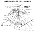
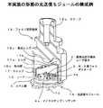
図1及び図2は本実施の形態の光送信モジュールの一例を示す構成図で、図1は本実施の形態の光送信モジュール1Aの要部構成を示す斜視図、図2は光送信モジュール1Aの全体構成を示す一部破断斜視図である。
次に、本実施の形態の光送信モジュール1Aの動作例について説明する。光送信モジュール1Aは、カソード側の電位をGNDとして面発光型半導体レーザ素子2がシングルエンド駆動される。面発光型半導体レーザ素子2は、電気信号を光信号に変換して、図示しない発光点から出射する。
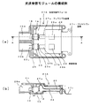
次に、上述した光送信モジュール1Aを備えた光送受信モジュールについて説明する。
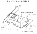
次に、上述した光送受信モジュール21Aを備えた光通信装置としてのネットワークカードについて説明する。
Claims (11)
- 電気信号を光信号に変換して出射する面発光素子と、
前記面発光素子に電気信号を供給する複数本のリードを有したステム部と、
前記ステム部の上面に実装されて接地されると共に、前記ステム部に対する上面に前記面発光素子を実装するチップ状コンデンサとを備え、
一の前記リードと前記面発光素子の一方の電極を導電性ワイヤで接続し、他の前記リードと前記チップ状コンデンサの上面電極を導電性ワイヤで接続すると共に、
前記チップ状コンデンサの前記上面電極に前記面発光素子を実装して、前記面発光素子の裏面に形成された他方の電極と前記上面電極を接続した
ことを特徴とする光送信モジュール。 - 前記チップ状コンデンサは、所定の周波数に対してバイパスコンデンサとして動作するために必要な容量を有すると共に、前記面発光素子を所定の高さに実装する厚さを有する
ことを特徴とする請求項1記載の光送信モジュール。 - 他の前記リードと前記チップ状コンデンサの上面電極を、1本もしくは複数本の前記導電性ワイヤで接続した
ことを特徴とする請求項1記載の光送信モジュール。 - 入射した光を電気信号に変換する受光素子と、
前記ステム部の上面に実装されると共に、前記ステム部に対する上面に前記受光素子を実装するチップ状コンデンサと、
前記面発光素子から出射された光の一部を前記受光素子へ入射させる光路形成部材を備えた
ことを特徴とする請求項1記載の光送信モジュール。 - 前記光路形成部材は、前記ステム部を封止するキャップ部材の窓部に取り付けられ、前記面発光素子から出射された光を透過すると共に、前記面発光素子から出射された光の一部を反射して、前記受光素子に入射させるレンズ部材である
ことを特徴とする請求項4記載の光送信モジュール。 - 光ファイバを支持するスリーブと、前記面発光素子から出射された光を集光する集光レンズと、前記ステム部に対する取付部を有したファイバ支持筐体が前記ステム部に取り付けられた
ことを特徴とする請求項1記載の光送信モジュール。 - 光信号を送信する光送信モジュールと、
光信号を受信する光受信モジュールと、
電気信号の処理を行う回路基板とを備え、
前記光送信モジュールは、
電気信号を光信号に変換して出射する面発光素子と、
前記面発光素子に電気信号を供給する複数本のリードを有したステム部と、
前記ステム部の上面に実装されて接地されると共に、前記ステム部に対する上面に前記面発光素子を実装するチップ状コンデンサとを備え、
一の前記リードと前記面発光素子の一方の電極を導電性ワイヤで接続し、他の前記リードと前記チップ状コンデンサの上面電極を導電性ワイヤで接続すると共に、
前記チップ状コンデンサの前記上面電極に前記面発光素子を実装して、前記面発光素子の裏面に形成された他方の電極と前記上面電極を接続した
ことを特徴とする光送受信モジュール。 - 前記回路基板は、
前記光送信モジュール及び前記光受信モジュールと接続される第1のフレキシブル基板と、
外部機器と接続される第2のフレキシブル基板と、
前記第1のフレキシブル基板及び前記第2のフレキシブル基板と接続され、送信側回路部及び受信側回路部が実装されたリジット基板とを備えた
ことを特徴とする請求項7記載の光送受信モジュール。 - 光信号を送受信する光送受信モジュールと、
前記光送受信モジュールが搭載される主基板とを備えた光通信装置において、
前記光送受信モジュールは、
光信号を送信する光送信モジュールと、
光信号を受信する光受信モジュールと、
電気信号の処理を行う回路基板とを備え、
前記光送信モジュールは、
電気信号を光信号に変換して出射する面発光素子と、
前記面発光素子に電気信号を供給する複数本のリードを有したステム部と、
前記ステム部の上面に実装されて接地されると共に、前記ステム部に対する上面に前記面発光素子を実装するチップ状コンデンサとを備え、
一の前記リードと前記面発光素子の一方の電極を導電性ワイヤで接続し、他の前記リードと前記チップ状コンデンサの上面電極を導電性ワイヤで接続すると共に、
前記チップ状コンデンサの前記上面電極に前記面発光素子を実装して、前記面発光素子の裏面に形成された他方の電極と前記上面電極を接続した
ことを特徴とする光通信装置。 - 前記回路基板は、
前記光送信モジュール及び前記光受信モジュールと接続される第1のフレキシブル基板と、
前記主基板と接続される第2のフレキシブル基板と、
前記第1のフレキシブル基板及び前記第2のフレキシブル基板と接続され、送信側回路部及び受信側回路部が実装されたリジット基板とを備えた
ことを特徴とする請求項9記載の光通信装置。 - 前記回路基板は、前記第1のフレキシブル基板及び前記第2のフレキシブル基板と、前記リジット基板が一体に形成されたフレックスリジット基板で構成される
ことを特徴とする請求項10記載の光通信装置。
Priority Applications (1)
| Application Number | Priority Date | Filing Date | Title |
|---|---|---|---|
| JP2005317098A JP2007123738A (ja) | 2005-10-31 | 2005-10-31 | 光送信モジュール、光送受信モジュール及び光通信装置 |
Applications Claiming Priority (1)
| Application Number | Priority Date | Filing Date | Title |
|---|---|---|---|
| JP2005317098A JP2007123738A (ja) | 2005-10-31 | 2005-10-31 | 光送信モジュール、光送受信モジュール及び光通信装置 |
Publications (1)
| Publication Number | Publication Date |
|---|---|
| JP2007123738A true JP2007123738A (ja) | 2007-05-17 |
Family
ID=38147219
Family Applications (1)
| Application Number | Title | Priority Date | Filing Date |
|---|---|---|---|
| JP2005317098A Pending JP2007123738A (ja) | 2005-10-31 | 2005-10-31 | 光送信モジュール、光送受信モジュール及び光通信装置 |
Country Status (1)
| Country | Link |
|---|---|
| JP (1) | JP2007123738A (ja) |
Cited By (2)
| Publication number | Priority date | Publication date | Assignee | Title |
|---|---|---|---|---|
| JP2013004945A (ja) * | 2011-06-22 | 2013-01-07 | Nippon Telegr & Teleph Corp <Ntt> | 光モジュール |
| JPWO2017188269A1 (ja) * | 2016-04-26 | 2019-02-28 | 京セラ株式会社 | 半導体パッケージおよびそれを用いた半導体装置 |
Citations (14)
| Publication number | Priority date | Publication date | Assignee | Title |
|---|---|---|---|---|
| JPH01138778A (ja) * | 1987-11-25 | 1989-05-31 | Mitsubishi Electric Corp | 半導体レーザ装置 |
| JPH02143208A (ja) * | 1988-11-25 | 1990-06-01 | Sumitomo Electric Ind Ltd | 光半導体素子モジュール |
| JPH03149510A (ja) * | 1989-11-07 | 1991-06-26 | Nippon Telegr & Teleph Corp <Ntt> | 半導体レーザ光ファイバ結合装置およびその製造方法 |
| JPH0464243A (ja) * | 1990-07-04 | 1992-02-28 | Hitachi Ltd | 半導体装置 |
| JPH04256378A (ja) * | 1991-02-08 | 1992-09-11 | Nec Corp | 光素子モジュール |
| JPH07221405A (ja) * | 1994-02-08 | 1995-08-18 | Sharp Corp | 半導体レーザ装置 |
| JPH07312430A (ja) * | 1994-05-16 | 1995-11-28 | Sumitomo Electric Ind Ltd | 光受信モジュ−ルとその製造方法 |
| JPH11354885A (ja) * | 1998-06-09 | 1999-12-24 | Toshiba Corp | 面発光型レーザ及び半導体発光装置 |
| JP2000340877A (ja) * | 1999-05-05 | 2000-12-08 | Mitel Semiconductor Ab | 垂直共振器型面発光レーザと光検出用モニターとのアセンブリー及びそのアセンブリング方法 |
| JP2003241029A (ja) * | 2002-02-14 | 2003-08-27 | Sumitomo Electric Ind Ltd | 光モジュールおよび光送受信器 |
| JP2004200210A (ja) * | 2002-12-16 | 2004-07-15 | Fuji Xerox Co Ltd | 面発光型半導体レーザ及びその製造方法 |
| JP2004281682A (ja) * | 2003-03-14 | 2004-10-07 | Sumitomo Electric Ind Ltd | 光送信装置 |
| JP2005062842A (ja) * | 2003-07-31 | 2005-03-10 | Toshiba Discrete Technology Kk | 光伝送デバイス |
| JP2005217284A (ja) * | 2004-01-30 | 2005-08-11 | Hitachi Cable Ltd | 光送受信モジュール |
-
2005
- 2005-10-31 JP JP2005317098A patent/JP2007123738A/ja active Pending
Patent Citations (14)
| Publication number | Priority date | Publication date | Assignee | Title |
|---|---|---|---|---|
| JPH01138778A (ja) * | 1987-11-25 | 1989-05-31 | Mitsubishi Electric Corp | 半導体レーザ装置 |
| JPH02143208A (ja) * | 1988-11-25 | 1990-06-01 | Sumitomo Electric Ind Ltd | 光半導体素子モジュール |
| JPH03149510A (ja) * | 1989-11-07 | 1991-06-26 | Nippon Telegr & Teleph Corp <Ntt> | 半導体レーザ光ファイバ結合装置およびその製造方法 |
| JPH0464243A (ja) * | 1990-07-04 | 1992-02-28 | Hitachi Ltd | 半導体装置 |
| JPH04256378A (ja) * | 1991-02-08 | 1992-09-11 | Nec Corp | 光素子モジュール |
| JPH07221405A (ja) * | 1994-02-08 | 1995-08-18 | Sharp Corp | 半導体レーザ装置 |
| JPH07312430A (ja) * | 1994-05-16 | 1995-11-28 | Sumitomo Electric Ind Ltd | 光受信モジュ−ルとその製造方法 |
| JPH11354885A (ja) * | 1998-06-09 | 1999-12-24 | Toshiba Corp | 面発光型レーザ及び半導体発光装置 |
| JP2000340877A (ja) * | 1999-05-05 | 2000-12-08 | Mitel Semiconductor Ab | 垂直共振器型面発光レーザと光検出用モニターとのアセンブリー及びそのアセンブリング方法 |
| JP2003241029A (ja) * | 2002-02-14 | 2003-08-27 | Sumitomo Electric Ind Ltd | 光モジュールおよび光送受信器 |
| JP2004200210A (ja) * | 2002-12-16 | 2004-07-15 | Fuji Xerox Co Ltd | 面発光型半導体レーザ及びその製造方法 |
| JP2004281682A (ja) * | 2003-03-14 | 2004-10-07 | Sumitomo Electric Ind Ltd | 光送信装置 |
| JP2005062842A (ja) * | 2003-07-31 | 2005-03-10 | Toshiba Discrete Technology Kk | 光伝送デバイス |
| JP2005217284A (ja) * | 2004-01-30 | 2005-08-11 | Hitachi Cable Ltd | 光送受信モジュール |
Cited By (2)
| Publication number | Priority date | Publication date | Assignee | Title |
|---|---|---|---|---|
| JP2013004945A (ja) * | 2011-06-22 | 2013-01-07 | Nippon Telegr & Teleph Corp <Ntt> | 光モジュール |
| JPWO2017188269A1 (ja) * | 2016-04-26 | 2019-02-28 | 京セラ株式会社 | 半導体パッケージおよびそれを用いた半導体装置 |
Similar Documents
| Publication | Publication Date | Title |
|---|---|---|
| CN100521887C (zh) | 具有陶瓷馈通头部组件的发射器光学子组件中的激光监视和控制 | |
| US7512165B2 (en) | Photoelectric conversion module and optical transceiver using the same | |
| JP5147832B2 (ja) | 光電子パッケージ、サブマウントアセンブリ及び光学サブアセンブリ | |
| JP5256620B2 (ja) | 光送信器および光受信器 | |
| US20030147601A1 (en) | Hybrid optical module employing integration of electronic circuitry with active optical devices | |
| US20030206703A1 (en) | Transmitters, receivers, and transceivers including an optical bench | |
| JP2020098837A (ja) | 光サブアッセンブリ及び光モジュール | |
| JP2005019717A (ja) | 通信モジュール | |
| JP2021044331A (ja) | 光サブアッセンブリ及び光モジュール | |
| JP2003229629A (ja) | 光モジュール | |
| JP3895331B2 (ja) | To−can構造の光モジュール | |
| JP5125235B2 (ja) | 光送受信装置および光送受信モジュール | |
| US10295768B2 (en) | Chip on leadframe optical subassembly | |
| US11057984B2 (en) | High-speed hybrid circuit | |
| JP2020021911A (ja) | 光サブアッセンブリ及び光モジュール | |
| JP2020021912A (ja) | 光サブアッセンブリ及び光モジュール | |
| JP4940628B2 (ja) | 光送信モジュール、光送受信モジュール及び光通信装置 | |
| JP2008226988A (ja) | 光電変換モジュール | |
| US6869230B2 (en) | Assembly for high-speed optical transmitter or receiver | |
| JP2004363360A (ja) | 光送受信モジュール | |
| US20050121736A1 (en) | Receiver optical subassembly | |
| JP2007121920A (ja) | 光モジュール、光通信モジュール及び光通信装置 | |
| US20040008953A1 (en) | Optical module and optical transceiver module | |
| JP2007123738A (ja) | 光送信モジュール、光送受信モジュール及び光通信装置 | |
| JP2004179559A (ja) | 光モジュール及びそれを用いた光モジュールアセンブリ |
Legal Events
| Date | Code | Title | Description |
|---|---|---|---|
| A621 | Written request for application examination |
Free format text: JAPANESE INTERMEDIATE CODE: A621 Effective date: 20080725 |
|
| RD02 | Notification of acceptance of power of attorney |
Free format text: JAPANESE INTERMEDIATE CODE: A7422 Effective date: 20090910 |
|
| RD04 | Notification of resignation of power of attorney |
Free format text: JAPANESE INTERMEDIATE CODE: A7424 Effective date: 20091106 |
|
| A977 | Report on retrieval |
Free format text: JAPANESE INTERMEDIATE CODE: A971007 Effective date: 20110119 |
|
| A131 | Notification of reasons for refusal |
Free format text: JAPANESE INTERMEDIATE CODE: A131 Effective date: 20110927 |
|
| A521 | Request for written amendment filed |
Free format text: JAPANESE INTERMEDIATE CODE: A523 Effective date: 20111117 |
|
| A02 | Decision of refusal |
Free format text: JAPANESE INTERMEDIATE CODE: A02 Effective date: 20111213 |