JP2007123738A - Optical transmission module, optical transmission / reception module, and optical communication device - Google Patents
Optical transmission module, optical transmission / reception module, and optical communication device Download PDFInfo
- Publication number
- JP2007123738A JP2007123738A JP2005317098A JP2005317098A JP2007123738A JP 2007123738 A JP2007123738 A JP 2007123738A JP 2005317098 A JP2005317098 A JP 2005317098A JP 2005317098 A JP2005317098 A JP 2005317098A JP 2007123738 A JP2007123738 A JP 2007123738A
- Authority
- JP
- Japan
- Prior art keywords
- optical
- light emitting
- emitting element
- optical transmission
- capacitor
- Prior art date
- Legal status (The legal status is an assumption and is not a legal conclusion. Google has not performed a legal analysis and makes no representation as to the accuracy of the status listed.)
- Pending
Links
Images

Classifications
-
- H—ELECTRICITY
- H10—SEMICONDUCTOR DEVICES; ELECTRIC SOLID-STATE DEVICES NOT OTHERWISE PROVIDED FOR
- H10W—GENERIC PACKAGES, INTERCONNECTIONS, CONNECTORS OR OTHER CONSTRUCTIONAL DETAILS OF DEVICES COVERED BY CLASS H10
- H10W72/00—Interconnections or connectors in packages
- H10W72/50—Bond wires
- H10W72/531—Shapes of wire connectors
- H10W72/536—Shapes of wire connectors the connected ends being ball-shaped
-
- H—ELECTRICITY
- H10—SEMICONDUCTOR DEVICES; ELECTRIC SOLID-STATE DEVICES NOT OTHERWISE PROVIDED FOR
- H10W—GENERIC PACKAGES, INTERCONNECTIONS, CONNECTORS OR OTHER CONSTRUCTIONAL DETAILS OF DEVICES COVERED BY CLASS H10
- H10W72/00—Interconnections or connectors in packages
- H10W72/50—Bond wires
- H10W72/531—Shapes of wire connectors
- H10W72/5363—Shapes of wire connectors the connected ends being wedge-shaped
-
- H—ELECTRICITY
- H10—SEMICONDUCTOR DEVICES; ELECTRIC SOLID-STATE DEVICES NOT OTHERWISE PROVIDED FOR
- H10W—GENERIC PACKAGES, INTERCONNECTIONS, CONNECTORS OR OTHER CONSTRUCTIONAL DETAILS OF DEVICES COVERED BY CLASS H10
- H10W72/00—Interconnections or connectors in packages
- H10W72/50—Bond wires
- H10W72/541—Dispositions of bond wires
- H10W72/547—Dispositions of multiple bond wires
- H10W72/5475—Dispositions of multiple bond wires multiple bond wires connected to common bond pads at both ends of the wires
Landscapes
- Semiconductor Lasers (AREA)
Abstract
【課題】高周波信号の伝送特性を向上させた安価な光送信モジュールを提供する。
【解決手段】光送信モジュール1Aは、ステム部5にマイクロチップコンデンサ4aとマイクロチップコンデンサ4bが実装され、マイクロチップコンデンサ4aの上面に面発光型半導体レーザ素子2が実装され、マイクロチップコンデンサ4bの上面にモニタ用フォトダイオード3が実装される。マイクロチップコンデンサ4aは、上面の電極が面発光型半導体レーザ素子2が実装される素子実装ランド6となり、面発光型半導体レーザ素子2のカソード端子2bが素子実装ランド6と接続されて、面発光型半導体レーザ素子2とマイクロチップコンデンサ4aは、ボンディングワイヤを介さずに直接接続される。
【選択図】 図1An inexpensive optical transmission module having improved high-frequency signal transmission characteristics is provided.
In an optical transmission module 1A, a microchip capacitor 4a and a microchip capacitor 4b are mounted on a stem portion 5, and a surface emitting semiconductor laser element 2 is mounted on the upper surface of the microchip capacitor 4a. A monitoring photodiode 3 is mounted on the upper surface. In the microchip capacitor 4a, the electrode on the upper surface becomes an element mounting land 6 on which the surface emitting semiconductor laser element 2 is mounted, and the cathode terminal 2b of the surface emitting semiconductor laser element 2 is connected to the element mounting land 6 so as to emit surface light. The type semiconductor laser element 2 and the microchip capacitor 4a are directly connected without a bonding wire.
[Selection] Figure 1
Description
本発明は、電気信号を光信号に変換して出力する光送信モジュール、この光送信モジュールを備えた光送受信モジュール及び光通信装置に関する。詳しくは、バイパスコンデンサとして動作させるチップ状コンデンサの上面電極に面発光素子を実装することで、面発光素子とチップ状コンデンサを直接接続して、高周波特性を向上させるようにしたものである。 The present invention relates to an optical transmission module that converts an electrical signal into an optical signal and outputs the optical signal, an optical transmission / reception module including the optical transmission module, and an optical communication device. Specifically, a surface light emitting element is mounted on the upper surface electrode of a chip capacitor that operates as a bypass capacitor, so that the surface light emitting element and the chip capacitor are directly connected to improve high frequency characteristics.
光モジュールの規格であるXFP(10Gigabit Small Form Factor Pluggable)モジュール等では、電気信号を光信号に変換して出力するため、半導体レーザ素子等を備えた光送信モジュールが実装されている。 In an XFP (10 Gigabit Small Form Factor Pluggable) module that is an optical module standard, an optical transmission module including a semiconductor laser element or the like is mounted in order to convert an electrical signal into an optical signal and output it.
光送信モジュールは、CANパッケージを構成するステム部の上面にサブマウント基板を実装し、サブマウント基板に半導体レーザ素子を実装する構成となっている。そして、半導体レーザ素子として、面発光型半導体レーザ素子(VCSEL)を使用する構成では、サブマウント基板の上面に面発光型半導体レーザ素子を実装して、焦点距離の調整を行っている(例えば、特許文献1参照)。 The optical transmission module has a configuration in which a submount substrate is mounted on an upper surface of a stem portion constituting a CAN package, and a semiconductor laser element is mounted on the submount substrate. In the configuration using a surface emitting semiconductor laser element (VCSEL) as the semiconductor laser element, the surface emitting semiconductor laser element is mounted on the upper surface of the submount substrate to adjust the focal length (for example, Patent Document 1).
さて、光送信モジュールでは、面発光型半導体レーザ素子をシングルエンド駆動する構成と差動駆動する構成が提案されている。データの転送速度が1Gbps〜10Gbpsを超えるような高速通信を行う場合、面発光型半導体レーザ素子をシングルエンド駆動する構成では、信号線とGNDの間に比較的容量の大きなコンデンサをシャント接続してバイパスコンデンサとして動作させて、GNDノイズ等を除去し、高周波特性を改善している。 Now, in the optical transmission module, a configuration in which the surface emitting semiconductor laser element is driven in a single end and a configuration in which it is differentially driven are proposed. When performing high-speed communication such that the data transfer rate exceeds 1 Gbps to 10 Gbps, in a configuration in which the surface emitting semiconductor laser element is single-ended driven, a capacitor having a relatively large capacity is shunt-connected between the signal line and GND. By operating as a bypass capacitor, GND noise and the like are removed, and high frequency characteristics are improved.
また、面発光型半導体レーザ素子を差動駆動する構成では、サブマウント基板の上面に一対の伝送線路を形成すると共に、インピーダンスの整合のために薄膜抵抗等を形成して、高周波特性を改善している。 In the configuration in which the surface emitting semiconductor laser device is differentially driven, a pair of transmission lines is formed on the upper surface of the submount substrate, and a thin film resistor is formed for impedance matching to improve high frequency characteristics. ing.
しかし、面発光型半導体レーザ素子をシングルエンド駆動する構成の光送信モジュールでは、サブマウント基板とコンデンサの双方を使用するので、部品点数が多く、コストが上昇するという問題がある。 However, the optical transmission module configured to single-end drive the surface emitting semiconductor laser element uses both the submount substrate and the capacitor, so that there is a problem that the number of parts is large and the cost is increased.
また、面発光型半導体レーザ素子とコンデンサをボンディングワイヤで接続しているので、高周波特性が悪化するという問題がある。 In addition, since the surface emitting semiconductor laser element and the capacitor are connected by a bonding wire, there is a problem that high frequency characteristics are deteriorated.
更に、面発光型半導体レーザ素子を差動駆動する構成の光送信モジュールでは、伝送線路の差動対称性を確保することが難しく、高周波特性を向上させることが困難であると共に、インピーダンス整合のための薄膜抵抗等が必要で、コストが上昇するという問題がある。 Further, in the optical transmission module configured to differentially drive the surface emitting semiconductor laser element, it is difficult to ensure the differential symmetry of the transmission line, it is difficult to improve the high frequency characteristics, and for impedance matching. However, there is a problem that the cost increases.
本発明は、このような課題を解決するためになされたもので、高周波信号の伝送特性を向上させた安価な光送信モジュール、この光送信モジュールを備えた光送受信モジュール及び光通信装置を提供することを目的とする。 The present invention has been made to solve such a problem, and provides an inexpensive optical transmission module with improved high-frequency signal transmission characteristics, an optical transmission / reception module and an optical communication device provided with the optical transmission module. For the purpose.
上述した課題を解決するため、本発明に係る光送信モジュールは、電気信号を光信号に変換して出射する面発光素子と、面発光素子に電気信号を供給する複数本のリードを有したステム部と、ステム部の上面に実装されて接地されると共に、ステム部に対する上面に面発光素子を実装するチップ状コンデンサとを備え、一のリードと面発光素子の一方の電極を導電性ワイヤで接続し、他のリードとチップ状コンデンサの上面電極を導電性ワイヤで接続すると共に、チップ状コンデンサの上面電極に面発光素子を実装して、面発光素子の裏面に形成された他方の電極とチップ状コンデンサの上面電極を接続したことを特徴とする。 In order to solve the above-described problems, an optical transmission module according to the present invention includes a surface light emitting element that converts an electric signal into an optical signal and emits the light, and a stem having a plurality of leads that supply the electric signal to the surface light emitting element. And a chip-like capacitor for mounting the surface light emitting element on the upper surface with respect to the stem part, and one lead and one electrode of the surface light emitting element are made of a conductive wire. Connect the other lead and the upper electrode of the chip capacitor with a conductive wire, and mount the surface light emitting element on the upper electrode of the chip capacitor and connect the other electrode formed on the back surface of the surface light emitting element. The upper surface electrode of the chip capacitor is connected.
本発明の光送信モジュールでは、面発光素子はシングルエンド駆動され、電気信号を光信号に変換して出射する。チップ状コンデンサは、シャント接続されていることで、バイパスコンデンサとして動作し、ノイズカット等を行う。 In the optical transmission module of the present invention, the surface light emitting element is single-ended driven, converts an electrical signal into an optical signal, and emits it. The chip-like capacitor operates as a bypass capacitor by being shunt-connected, and performs noise cutting and the like.
本発明に係る光送受信モジュールは、光信号を送信する光送信モジュールと、光信号を受信する光受信モジュールと、電気信号の処理を行う回路基板とを備え、光送信モジュールは、電気信号を光信号に変換して出射する面発光素子と、面発光素子に電気信号を供給する複数本のリードを有したステム部と、ステム部の上面に実装されて接地されると共に、ステム部に対する上面に面発光素子を実装するチップ状コンデンサとを備え、一のリードと面発光素子の一方の電極を導電性ワイヤで接続し、他のリードとチップ状コンデンサの上面電極を導電性ワイヤで接続すると共に、チップ状コンデンサの上面電極に面発光素子を実装して、面発光素子の裏面に形成された他方の電極とチップ状コンデンサの上面電極を接続したことを特徴とする。 An optical transmission / reception module according to the present invention includes an optical transmission module that transmits an optical signal, an optical reception module that receives the optical signal, and a circuit board that performs processing of the electric signal. A surface light emitting element that converts and emits a signal, a stem portion having a plurality of leads for supplying an electric signal to the surface light emitting element, and is mounted on the upper surface of the stem portion and grounded, and on the upper surface with respect to the stem portion A chip-like capacitor for mounting the surface light-emitting element, one lead and one electrode of the surface light-emitting element are connected by a conductive wire, and the other lead and the upper electrode of the chip-like capacitor are connected by a conductive wire The surface light emitting device is mounted on the upper surface electrode of the chip-shaped capacitor, and the other electrode formed on the back surface of the surface light emitting device is connected to the upper surface electrode of the chip-shaped capacitor.
本発明の光送受信モジュールでは、光送信モジュールで電気信号を光信号に変換して出力すると共に、光受信モジュールで光信号を受信して、電気信号に変換して出力する。 In the optical transmission / reception module of the present invention, the optical transmission module converts an electrical signal into an optical signal and outputs it, and the optical reception module receives the optical signal, converts it into an electrical signal, and outputs it.
光送信モジュールでは、面発光素子はシングルエンド駆動され、電気信号を光信号に変換して出射する。チップ状コンデンサは、シャント接続されていることで、バイパスコンデンサとして動作し、ノイズカット等を行う。 In the optical transmission module, the surface light emitting element is single-ended driven, converts an electrical signal into an optical signal, and emits it. The chip-like capacitor operates as a bypass capacitor by being shunt-connected, and performs noise cutting and the like.
本発明に係る光通信装置は、光信号を送受信する光送受信モジュールと、光送受信モジュールが搭載される主基板とを備えた光通信装置において、光送受信モジュールは、光信号を送信する光送信モジュールと、光信号を受信する光受信モジュールと、電気信号の処理を行う回路基板とを備え、光送信モジュールは、電気信号を光信号に変換して出射する面発光素子と、面発光素子に電気信号を供給する複数本のリードを有したステム部と、ステム部の上面に実装されて接地されると共に、ステム部に対する上面に面発光素子を実装するチップ状コンデンサとを備え、一のリードと面発光素子の一方の電極を導電性ワイヤで接続し、他のリードとチップ状コンデンサの上面電極を導電性ワイヤで接続すると共に、チップ状コンデンサの上面電極に面発光素子を実装して、面発光素子の裏面に形成された他方の電極とチップ状コンデンサの上面電極を接続したことを特徴とする。 An optical communication apparatus according to the present invention includes an optical transmission / reception module that transmits / receives an optical signal and a main board on which the optical transmission / reception module is mounted. The optical transmission / reception module transmits an optical signal. A light receiving module for receiving an optical signal, and a circuit board for processing the electric signal. The optical transmission module converts the electric signal into an optical signal and emits the light, and the surface light emitting element is electrically connected. A stem portion having a plurality of leads for supplying a signal, and a chip capacitor mounted on the upper surface of the stem portion and grounded, and mounted with a surface light emitting element on the upper surface with respect to the stem portion; One electrode of the surface light emitting element is connected by a conductive wire, the other lead and the upper surface electrode of the chip capacitor are connected by a conductive wire, and the upper surface current of the chip capacitor is also connected. Implementing a surface emitting element, characterized in that connecting the upper surface electrode of the other electrode and the chip-shaped capacitor formed on the back surface of the surface light-emitting element.
本発明の光通信装置では、光送受信モジュールにより光信号が送受信される。光送受信モジュールでは、光送信モジュールで電気信号を光信号に変換して出力すると共に、光受信モジュールで光信号を受信して、電気信号に変換して出力する。 In the optical communication apparatus of the present invention, an optical signal is transmitted and received by the optical transceiver module. In the optical transmission / reception module, the optical transmission module converts an electrical signal into an optical signal and outputs it, and the optical reception module receives the optical signal, converts it into an electrical signal, and outputs it.
光送信モジュールでは、面発光素子はシングルエンド駆動され、電気信号を光信号に変換して出射する。チップ状コンデンサは、シャント接続されていることで、バイパスコンデンサとして動作し、ノイズカット等を行う。 In the optical transmission module, the surface light emitting element is single-ended driven, converts an electrical signal into an optical signal, and emits it. The chip-like capacitor operates as a bypass capacitor by being shunt-connected, and performs noise cutting and the like.
本発明の光送信モジュールによれば、面発光素子にチップ状コンデンサを接続して、バイパスコンデンサとして動作させることで、シングルエンド駆動におけるノイズの影響等を低減させると共に、導電性ワイヤを介在させることなく、面発光素子とチップ状コンデンサを直接接続することで、高周波特性を向上させることができる。 According to the optical transmission module of the present invention, a chip-like capacitor is connected to the surface light emitting element to operate as a bypass capacitor, thereby reducing the influence of noise in single-ended driving and interposing a conductive wire. Instead, the high frequency characteristics can be improved by directly connecting the surface light emitting element and the chip capacitor.
また、サブマウント基板を使用することなく、面発光素子を所定の高さに実装することができるので、部品点数を削減して、コストを低減することができる。 Further, since the surface light emitting element can be mounted at a predetermined height without using the submount substrate, the number of parts can be reduced and the cost can be reduced.
本発明の光送受信モジュール及び光通信装置によれば、上述した光送信モジュールを備えることで、データの転送速度を向上させ、かつ安定した光通信を行うことができる。また、光送受信モジュール及び光通信装置を安価に提供することができる。 According to the optical transmission / reception module and the optical communication device of the present invention, by providing the above-described optical transmission module, it is possible to improve the data transfer rate and perform stable optical communication. In addition, the optical transceiver module and the optical communication device can be provided at low cost.
以下、図面を参照して本発明の光送信モジュール、光送受信モジュール及び光通信装置の実施の形態について説明する。 Embodiments of an optical transmission module, an optical transmission / reception module, and an optical communication device according to the present invention will be described below with reference to the drawings.
<本実施の形態の光送信モジュールの構成例>
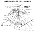
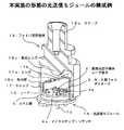
図1及び図2は本実施の形態の光送信モジュールの一例を示す構成図で、図1は本実施の形態の光送信モジュール1Aの要部構成を示す斜視図、図2は光送信モジュール1Aの全体構成を示す一部破断斜視図である。
<Configuration example of optical transmission module of the present embodiment>
1 and 2 are configuration diagrams showing an example of an optical transmission module according to the present embodiment. FIG. 1 is a perspective view showing a main configuration of the optical transmission module 1A according to the present embodiment. FIG. 2 shows the optical transmission module 1A. It is a partially broken perspective view which shows the whole structure.
本実施の形態の光送信モジュール1Aは、TOSA(Transmitter Optical SubAssembly)と称され、面発光型半導体レーザ素子2とモニタ用フォトダイオード3を備える。面発光型半導体レーザ素子2は、所定の高さを有したマイクロチップコンデンサ4aを介してステム部5に実装されて、焦点距離が合わせられている。同様に、モニタ用フォトダイオード3もマイクロチップコンデンサ4bを介してステム部5に実装される。
The optical transmission module 1A according to the present embodiment is referred to as TOSA (Transmitter Optical SubAssembly), and includes a surface emitting
面発光型半導体レーザ素子(VCSEL)2は面発光素子の一例で、入力された電気信号を光信号に変換する。面発光型半導体レーザ素子2は、図示しない基板と垂直方向に共振器が形成されて、素子の表面側から光を出射する。また、本実施の形態の面発光型半導体レーザ素子2は、一例としてN−subであり、表面側に一方の電極としてアノード端子2aが形成されると共に、裏面側に他方の電極としてカソード端子2bが形成される。
A surface emitting semiconductor laser element (VCSEL) 2 is an example of a surface emitting element, and converts an input electric signal into an optical signal. The surface-emitting type
モニタ用フォトダイオード3は受光素子の一例で、素子の表面側から光が入射され、入射された光信号を電気信号に変換して出力する。本例のモニタ用フォトダイオード3は、表面に電極としてアノード端子3aとカソード端子3bが形成されている。
The
マイクロチップコンデンサ4aは、誘電体を挟んで上下面に電極が形成され、上面電極が素子実装ランド6となり、面発光型半導体レーザ素子2が実装される。マイクロチップコンデンサ4aと面発光型半導体レーザ素子2は、素子実装ランド6に面発光型半導体レーザ素子2のカソード端子2bを、銀ペースト等の導電性を有した接合部材で実装するので、ボンディングワイヤを介することなく、直接接続される。
In the microchip capacitor 4a, electrodes are formed on the upper and lower surfaces with a dielectric in between, the upper surface electrode serves as an element mounting land 6, and the surface emitting
ここで、マイクロチップコンデンサ4aは、所望の周波数に対してバイパスコンデンサとして動作させるため、所定の容量が必要である。 Here, since the microchip capacitor 4a operates as a bypass capacitor with respect to a desired frequency, a predetermined capacity is required.
また、マイクロチップコンデンサ4aは、素子実装ランド6に面発光型半導体レーザ素子2を実装すると共に、後述するリードと接続されるボンディングワイヤを接続するために、素子実装ランド6となる電極の大きさが、面発光型半導体レーザ素子2よりも大きい必要がある。
The microchip capacitor 4a has a size of an electrode to be the element mounting land 6 for mounting the surface emitting
更に、マイクロチップコンデンサ4aは、面発光型半導体レーザ素子2の高さ調整を行って、面発光型半導体レーザ素子2から出射された光の焦点距離を合わせるために、所定の厚さが必要である。
Further, the microchip capacitor 4a needs to have a predetermined thickness in order to adjust the height of the surface emitting
従って、マイクロチップコンデンサ4aとしては、以上のような条件を満たすものが選択されて使用される。 Therefore, a microchip capacitor 4a that satisfies the above conditions is selected and used.
マイクロチップコンデンサ4bは、マイクロチップコンデンサ4aと同様に誘電体を挟んで上下面に電極が形成され、上面電極にモニタ用フォトダイオード3が銀ペースト等で実装される。
Similarly to the microchip capacitor 4a, the
ステム部5は円板形状で、複数本のリード12を備える。複数本のリードの中の4本のリード12a〜12dは、ステム部5を貫通して取り付けられており、一方の端部となる上端がステム部5の上面から露出している。また、ステム部5は金属で作製され、各リード12a〜12dは、ガラス等の絶縁層13を介してステム部5に支持されて、ステム部5とは絶縁されている。
The
マイクロチップコンデンサ4aは、ステム部5の上面の中心付近に銀ペースト等で実装され、ステム部5を介してGNDに接地される。また、マイクロチップコンデンサ4bは、リード12cとリード12dの間のステム部5の上面に、マイクロチップコンデンサ4aと並列して銀ペースト等で実装される。
The microchip capacitor 4 a is mounted with silver paste or the like near the center of the upper surface of the
リード12aは、面発光型半導体レーザ素子2のアノード端子2aと導電性ワイヤであるボンディングワイヤ14aによって接続される。また、リード12bは、マイクロチップコンデンサ4aの素子実装ランド6と導電性ワイヤであるボンディングワイヤ14bによって接続される。上述したように、マイクロチップコンデンサ4aの素子実装ランド6には、面発光型半導体レーザ素子2が実装されることで、リード12bは面発光型半導体レーザ素子2のカソード端子2bと接続されることになる。
The lead 12a is connected to the anode terminal 2a of the surface emitting
ここで、本実施の形態の面発光型半導体レーザ素子2はN−subで、シングルエンド駆動であるため、カソード側がGNDとなる。このため、ボンディングワイヤ14bのインダクタンスの大きさが無視できないので、マイクロチップコンデンサ4aの素子実装ランド6とリード12bを接続するボンディングワイヤ14bは、少なくとも2本以上とする。
Here, the surface-emitting type
また、マイクロチップコンデンサ4bに実装されたモニタ用フォトダイオード3のアノード端子3aとリード12cがボンディングワイヤ14cによって接続され、モニタ用フォトダイオード3のカソード端子3bとリード12dがボンディングワイヤ14dによって接続される。
Further, the
光送信モジュール1Aは、キャップ17とファイバ支持筐体18を備える。キャップ17はキャップ部材の一例で、端部に形成される窓部17bにレンズ17aを備えた円筒形状で、ステム部5に被せられる。レンズ17aは、モニタ用フォトダイオード3に向けて傾斜しており、面発光型半導体レーザ素子2から出射された光を所定の透過率で透過すると共に、一部の光をモニタ用フォトダイオード3に向けて反射する。
The
本実施の形態の光送信モジュール1Aでは、面発光型半導体レーザ素子2をマイクロチップコンデンサ4aの上面に実装し、モニタ用フォトダイオード3をマイクロチップコンデンサ4bの上面に実装することで、面発光型半導体レーザ素子2から出射され、キャップ17のレンズ17aで反射した光がモニタ用フォトダイオード3に入射するように、レンズ17aに対する面発光型半導体レーザ素子2及びモニタ用フォトダイオード3の高さが調整される。
In the optical transmission module 1A of the present embodiment, the surface-emitting type
これにより、面発光型半導体レーザ素子2から出射された光の一部をモニタ用フォトダイオード3で受信して、面発光型半導体レーザ素子2の発光量のモニタリングが行われる。
As a result, a part of the light emitted from the surface emitting
ファイバ支持筐体18は、図示しない光ファイバを支持するスリーブ18aと、ステム部5に対する取付部18bと、面発光型半導体レーザ素子2から出射された光を集光する集光レンズ18cを備える。
The
ファイバ支持筐体18は、面発光型半導体レーザ素子2から出射される光の波長に対して所定の透過率を有した透明な樹脂で、スリーブ18aと取付部18bと集光レンズ18cが一体に形成される。
The
スリーブ18aは、ファイバ支持筐体18の一端側に形成され、図示しない光ファイバのフェルールが着脱自在に挿抜される円筒状の空間を有する。取付部18bは、ファイバ支持筐体18の他端側に形成され、ステム部5に取り付けられたキャップ17に嵌る形状の空間を有する。取付部18bは、内部中央に面発光型半導体レーザ素子2と対向して集光レンズ18cが形成される。
The sleeve 18a is formed on one end side of the
集光レンズ18cは、スリーブ18aに支持される図示しない光ファイバと同軸上に形成され、面発光型半導体レーザ素子2側に突出した凸レンズで、面発光型半導体レーザ素子2から出射された光を、スリーブ18aで支持された光ファイバの端面に集光する。
The condensing lens 18c is a convex lens that is formed coaxially with an optical fiber (not shown) supported by the sleeve 18a and protrudes toward the surface-emitting type
そして、本実施の形態の光送信モジュール1Aでは、面発光型半導体レーザ素子2をマイクロチップコンデンサ4aの上面に実装することで、面発光型半導体レーザ素子2から出射された光が、スリーブ18aで支持された光ファイバの端面に集光するように、焦点距離が調整される。
In the optical transmission module 1A of the present embodiment, the surface emitting
ここで、ファイバ支持筐体18の取付部18bの内径は、ステム部5に取り付けられたキャップ17の外径より若干大きく構成され、面発光型半導体レーザ素子2から出射される光の光軸に対して直交する方向に、ファイバ支持筐体18の位置を調整することが可能である。これにより、面発光型半導体レーザ素子2に対して、スリーブ18aで支持される光ファイバの光軸合わせが可能な構成となっている。
Here, the inner diameter of the attachment portion 18b of the
なお、以上の例では、面発光型半導体レーザ素子2として、N−subの面発光型半導体レーザ素子を使用する構成で説明したが、P−subの面発光型半導体レーザ素子を使用する構成としてもよい。P−subの面発光型半導体レーザ素子を使用する構成では、リード12aをカソード側とし、リード12bをアノード側とする。
In the above example, the configuration using an N-sub surface emitting semiconductor laser element as the surface emitting
P−subの面発光型半導体レーザ素子では、表面側の電極がカソード電極となり、リード12aとボンディングワイヤ14aで接続される。また、面発光型半導体レーザ素子の裏面側の電極がアノード電極となり、マイクロチップコンデンサ4aの上面電極である素子実装ランド6に直接接続される。また、マイクロチップコンデンサ4aの素子実装ランド6とリード12bがボンディングワイヤ14bで接続される。
In the P-sub surface emitting semiconductor laser element, the electrode on the front surface side becomes a cathode electrode and is connected to the lead 12a and the
<本実施の形態の光送信モジュールの動作例>
次に、本実施の形態の光送信モジュール1Aの動作例について説明する。光送信モジュール1Aは、カソード側の電位をGNDとして面発光型半導体レーザ素子2がシングルエンド駆動される。面発光型半導体レーザ素子2は、電気信号を光信号に変換して、図示しない発光点から出射する。
<Operation example of optical transmission module of this embodiment>
Next, an operation example of the optical transmission module 1A of the present embodiment will be described. In the optical transmission module 1A, the surface-emitting type
面発光型半導体レーザ素子2から出射された光は、キャップ17のレンズ17aを透過し、ファイバ支持筐体18の集光レンズ18cに入射する。集光レンズ18cに入射した光は、スリーブ18aに挿入されて支持されている図示しない光ファイバの端面に集光することで、光ファイバに入射して伝送される。
The light emitted from the surface emitting
また、面発光型半導体レーザ素子2から出射された光の一部は、キャップ17のレンズ17aで反射して、モニタ用フォトダイオード3に入射する。モニタ用フォトダイオード3に入射した光は電気信号に変換されて出力され、リード12c,12dを介して接続されている図示しない回路によって、面発光型半導体レーザ素子2の発光量のモニタリングが行われる。
Further, part of the light emitted from the surface emitting
面発光型半導体レーザ素子を差動駆動する構成では、伝送線路の差動対象性を確保しないと、高周波信号の伝送特性が悪化する。これに対して、面発光型半導体レーザ素子をシングエンド駆動する構成では、伝送線路の差動対象性を考慮する必要がない。 In the configuration in which the surface-emitting type semiconductor laser element is differentially driven, the transmission characteristics of the high-frequency signal are deteriorated unless the differential subjectivity of the transmission line is ensured. On the other hand, in the configuration in which the surface emitting semiconductor laser element is driven in a single end, there is no need to consider the differential subjectivity of the transmission line.
但し、シングルエンド駆動では、GNDノイズ等の影響を排除する必要がある。そこで、上述したように、面発光型半導体レーザ素子2のカソード端子2bには、マイクロチップコンデンサ4aが接続されている。
However, in the single end drive, it is necessary to eliminate the influence of GND noise and the like. Therefore, as described above, the microchip capacitor 4 a is connected to the
そして、所望の容量を有したマイクロチップコンデンサ4aを使用することで、マイクロチップコンデンサ4aがバイパスコンデンサとして動作し、ノイズカット等が行われる。これにより、シングルエンド駆動であっても、高周波特性を向上させることができる。 Then, by using the microchip capacitor 4a having a desired capacity, the microchip capacitor 4a operates as a bypass capacitor, and noise cut or the like is performed. As a result, high-frequency characteristics can be improved even with single-end driving.
なお、マイクロチップコンデンサ4aとしては、バイパスコンデンサとして動作させるために必要な比較的容量の大きなものを、汎用の市販品を使用して実現することが可能である。 As the microchip capacitor 4a, a comparatively large capacitor necessary for operating as a bypass capacitor can be realized using a general-purpose commercial product.
さて、面発光型半導体レーザ素子2とマイクロチップコンデンサ4aをボンディングワイヤを介して接続する構成では、伝送される信号が高周波になると、ボンディングワイヤのL(インダクタンス)成分が大きくなるので、マイクロチップコンデンサ4aの自己共振周波数が低くなってしまい、純粋な特性が得られない。これにより、高周波特性が悪化する。
In the configuration in which the surface emitting
これに対して、面発光型半導体レーザ素子2をマイクロチップコンデンサ4aの上面の電極である素子実装ランド6に実装することで、面発光型半導体レーザ素子2のカソード端子2bとマイクロチップコンデンサ4aが、ボンディングワイヤを介さずに直接接続される。
On the other hand, by mounting the surface emitting
これにより、面発光型半導体レーザ素子2に対して、対GNDにコンデンサが直接取り付けられることになり、高周波特性が向上する。
As a result, a capacitor is directly attached to GND with respect to the surface-emitting type
また、面発光型半導体レーザ素子2をマイクロチップコンデンサ4aの上面に実装すると共に、モニタ用フォトダイオード3をマイクロチップコンデンサ4bの上面に実装することで、面発光型半導体レーザ素子2とモニタ用フォトダイオード3が、サブマウント基板を使用することなく所定の高さに実装される。
In addition, the surface emitting
これにより、部品点数を減らしてコストを低減することができる。一例として、マイクロチップコンデンサ4a,4bは、容量及び高さの両面で、汎用の市販品を使用できるのに対して、サブマウント基板は、光送信モジュールの仕様に合わせたものを作製する必要がある。このため、サブマウント基板を使用しない構成とすれば、コストを低減することができる。
Thereby, the number of parts can be reduced and cost can be reduced. As an example, for the
図3は伝送信号のアイダイヤグラムの比較例で、図3(a)は本実施の形態の光送信モジュール1Aにおけるアイダイヤグラムを示し、図3(b)は比較例としてサブマウント基板に面発光型半導体レーザ素子を実装した従来の光送信モジュールにおけるアイダイヤグラムを示す。なお、本例の光送信モジュール1Aでは、面発光型半導体レーザ素子2はN−sub、マイクロチップコンデンサ4a,4bの容量は360pFとした。
FIG. 3 is a comparative example of an eye diagram of a transmission signal, FIG. 3A shows an eye diagram in the optical transmission module 1A of the present embodiment, and FIG. 3B is a surface emitting type on a submount substrate as a comparative example. The eye diagram in the conventional optical transmission module which mounted the semiconductor laser element is shown. In the optical transmission module 1A of this example, the surface emitting
図3(b)に示すように、従来の光送信モジュールでは、アイ開口が狭くジッターが増加している。これに対して、本実施の形態の光送信モジュール1Aでは、十分な容量を有したマイクロチップコンデンサ4a,4bを使用し、かつ面発光型半導体レーザ素子2とマイクロチップコンデンサ4aをボンディングワイヤを使用せずに直接接続したので、図3(a)に示すように、ジッター、オーバーシュート及びアンダーシュートが抑えられ、アイ開口が広くなっている。これにより、高周波信号の伝送特性が向上していることが確認できる。
As shown in FIG. 3B, the conventional optical transmission module has a narrow eye opening and increased jitter. On the other hand, in the optical transmission module 1A of the present embodiment, the
<本実施の形態の光送受信モジュールの構成例>
次に、上述した光送信モジュール1Aを備えた光送受信モジュールについて説明する。
<Configuration example of optical transceiver module of this embodiment>
Next, an optical transmission / reception module including the above-described optical transmission module 1A will be described.
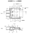
図4は本実施の形態の光送受信モジュールの一例を示す構成図で、図4(a)は光送受信モジュール21Aの平面断面図、図4(b)は図4(a)に示す光送受信モジュール21AのA−A断面図である。 FIG. 4 is a block diagram showing an example of the optical transceiver module of the present embodiment. FIG. 4A is a plan sectional view of the optical transceiver module 21A, and FIG. 4B is the optical transceiver module shown in FIG. It is AA sectional drawing of 21A.
本実施の形態の光送受信モジュール21Aは、光信号を送信する上述した光送信モジュール1Aと、光信号を受信する光受信モジュール23と、電気信号の処理を行う回路基板24と、筐体25を備える。
The optical transmission / reception module 21A of the present embodiment includes the above-described optical transmission module 1A that transmits an optical signal, the
光受信モジュール23は、ROSA(Receiver Optical SubAssembly)と称され、例えば、フォトダイオード等がステム部23aに実装される。ステム部23aは、フォトダイオードと接続される複数本のリード23bを備え、各リード23bがステム部23aの後面から突出している。また、受信モジュール23は、図示しない光ファイバを支持するスリーブと、集光レンズ等を有したファイバ支持筐体23cがステム部23aに取り付けられる。
The
回路基板24は、リジット基板26と、フレキシブル基板27a〜27cを備え、例えばリジット基板26とフレキシブル基板27a〜27cが一体に構成されたフレックスリジット基板である。なお、回路基板24としては、リジット基板26にフレキシブル基板27a〜27cが半田付けで接続される構成でもよい。
The
回路基板24は、リジット基板26の一端側に、光送信モジュール1Aと光受信モジュール23に対応して、第1のフレキシブル基板である2本のフレキシブル基板27a,27bを備える。また、リジット基板26の他端側に、後述するホストボード等と接続される第2のフレキシブル基板であるフレキシブル基板27cを備える。
The
リジット基板26は、光送信モジュール1Aを動作させるための送信側回路部として、例えば、駆動回路であるレーザドライバIC(Integrated Circuit)や、バイアス回路、APC回路等を構成する単数あるいは複数のICチップ26a等が搭載される。また、リジット基板26は、光受信モジュール23を動作させるための受信側回路部として、増幅回路であるLA(Limiting Amplifier)−ICや、受信光パワー検出回路等を構成する単数あるいは複数のICチップ26b等が搭載される。なお、増幅回路としてLA−ICは一例で、LA−ICが搭載されない構成でもよい。
The
フレキシブル基板27a〜27cは、例えば、図1に示すように、一方の面は信号配線層でマイクロストリップライン27Sが形成され、他方の面は接地導体層で所定のGNDパターン27Gが形成されることで、インピーダンスコントロールを行っている。そして、フレキシブル基板27aには、図1で説明した光送信モジュール1Aの各リード12が半田付けにより接続され、フレキシブル基板27bには光受信モジュール23のリード23bが半田付けにより接続される。なお、インピーダンスコントロールラインは、GNDパターン等によらずに形成することも可能である。
For example, as shown in FIG. 1, the
筐体25は、光送信モジュール1A、光受信モジュール23及び回路基板24が取り付けられる。筐体25は、光送信モジュール1Aのファイバ支持筐体18に対応してコネクタ部25aが形成されると共に、光受信モジュール23のファイバ支持筐体23cに対応してコネクタ部25bが形成される。
The optical transmitter module 1A, the
また、筐体25は、内部に回路基板24のリジット基板26が固定され、筐体25の他端側から外部接続用にフレキシブル基板27cが露出する。ここで、光送信モジュール1Aとリジット基板26はフレキシブル基板27aで接続され、光受信モジュール23とリジット基板26はフレキシブル基板27bで接続されているので、筐体25に固定される光送信モジュール1A及び光受信モジュール23と、リジット基板26の位置の誤差は、フレキシブル基板27a,27bの変形で吸収される。
Further, the
<本実施の形態の光通信装置の構成例>
次に、上述した光送受信モジュール21Aを備えた光通信装置としてのネットワークカードについて説明する。
<Example of Configuration of Optical Communication Device of this Embodiment>
Next, a network card as an optical communication apparatus provided with the above-described optical transceiver module 21A will be described.
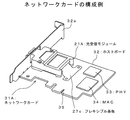
図5は本実施の形態のネットワークカードの一例を示す斜視図である。本実施の形態のネットワークカード31Aは、図4で説明した光送受信モジュール21Aと、ホストボード32を備える。
FIG. 5 is a perspective view showing an example of the network card according to the present embodiment. The
ホストボード32は主基板の一例で、一端側に光送受信モジュール21Aが実装される。ホストボード32は、一端にベゼル32aが取り付けられ、光送受信モジュール21Aのコネクタ部25a,25bがベゼル32aに露出するように実装される。
The
また、ホストボード32は、他端側に例えばPHY(Physical layer)用チップ33と、MAC(Media Access Control)用チップ34等が実装される。なお、例えば、PHY用チップをホストボードに搭載せずに光送受信モジュール21Aに搭載し、光送受信モジュール21Aが直接MAC用チップ34に接続される構成でもよい。更に、ホストボード32は、一方の側端にPCI−Express等のカードエッジコネクタ35を備える。
The
ネットワークカード31Aでは、ホストボード32と光送受信モジュール21Aの電気的接続は、光送受信モジュール21Aに備えたフレキシブル基板27cにより行われる。フレキシブル基板27cは、例えば、ホストボード32に形成された所定の電極パッドに半田付けによって接続される。なお、ホストボード32にコネクタを備え、フレキシブル基板27cをコネクタに接続する構成としてもよい。
In the
ネットワークカード31Aは、パーソナルコンピュータ等の拡張スロットに搭載され、カードエッジコネクタ35がパーソナルコンピュータ側のコネクタと接続される。
The
さて、光送受信モジュール21Aは、上述したように、コネクタ部25a,25bをベゼル部32aに露出させるが、コネクタ部25a,25bの端面を所定の位置に揃えるように実装すれば、外観性が向上する。但し、各部の寸法上の誤差により、光送受信モジュール21Aのホストボード32上での位置に誤差が生じる。
As described above, the optical transmission / reception module 21A exposes the connector portions 25a and 25b to the bezel portion 32a. However, if mounted so that the end surfaces of the connector portions 25a and 25b are aligned at predetermined positions, the appearance is improved. To do. However, an error occurs in the position of the optical transmission / reception module 21A on the
そこで、本実施の形態のネットワークカード31Aでは、ホストボード32と光送受信モジュール21Aの電気的接続を、光送受信モジュール21Aに備えたフレキシブル基板27cにより行うことで、光送受信モジュール21Aのホストボード32上での位置の誤差を、フレキシブル基板27cの変形で吸収する。
Therefore, in the
これにより、ネットワークカード31Aでは、光送受信モジュール21Aを、コネクタ部25a,25bの端面が所定の位置に揃うように実装することができ、外観性が向上する。
Thereby, in the
また、光送受信モジュール21Aにおいて、図4(a)に示すように、光送信モジュール1Aはフレキシブル基板27aでリジット基板26と接続され、光受信モジュール23はフレキシブル基板27bでリジット基板26に接続される。これにより、光ファイバのコネクタを挿抜する際の衝撃をフレキシブル基板27a,27bで吸収して、リジット基板26に伝わらないようにすることができる。
In the optical transceiver module 21A, as shown in FIG. 4A, the optical transmission module 1A is connected to the
次に、本実施の形態のネットワークカード31Aの動作について説明する。ネットワークカード31Aは、光送受信モジュール21Aのコネクタ部25a,25bに図示しない光ファイバが接続され、外部の情報通信機器等との間でデータの送受信が光信号によって行われる。
Next, the operation of the
まず、データを送信する動作について説明すると、ネットワークカード31Aは、パーソナルコンピュータ等の拡張スロットに接続されたカードエッジコネクタ35を介して、送信されるデータが入力される。
First, the operation of transmitting data will be described. Data to be transmitted is input to the
送信されるデータは、MAC用チップ34及びPHY用チップ33等により処理が行われ、フレキシブル基板27cを介して光送受信モジュール21Aの回路基板24に入力される。
Data to be transmitted is processed by the
光送受信モジュール21Aは、回路基板24のリジット基板26に実装されたレーザドライバIC等のICチップ26a等により、送信されるデータの処理を行い、フレキシブル基板27aを介して光送信モジュール1Aの面発光型半導体レーザ素子2に出力する。
The optical transmission / reception module 21A processes data to be transmitted by an IC chip 26a such as a laser driver IC mounted on the
面発光型半導体レーザ素子2は、送信されるデータに応じた電気信号を光信号に変換して出射する。これにより、面発光型半導体レーザ素子2から出射された光信号は図示しない光ファイバを伝送され、外部の情報通信機器に対してデータの送信が行われる。
The surface emitting
さて、ネットワークカード31Aに搭載される光送信モジュール1Aは、図1等で説明したように、バイパスコンデンサとして動作するために十分な容量を有したマイクロチップコンデンサ4a,4bを使用し、かつ面発光型半導体レーザ素子2とマイクロチップコンデンサ4aをボンディングワイヤを使用せずに直接接続したので、1Gbps〜10Gbpsを超えるような高周波信号の伝送特性が向上しており、通信の品質を劣化させることなく、データの転送速度を向上させることができる。
Now, the optical transmission module 1A mounted on the
また、マイクロチップコンデンサ4aの上面に面発光型半導体レーザ素子2を実装し、マイクロチップコンデンサ4bの上面にモニタ用フォトダイオードを実装することで、サブマウント基板を使用することなく、面発光半導体レーザ素子2及びモニタ用フォトダイオード3を所定の高さに実装している。
Further, by mounting the surface emitting
これにより、光送信モジュール1Aのコストを低減することができ、高周波特性が向上した光送受信モジュール21A及びネットワークカード31Aを、安価に提供できる。
Thereby, the cost of the optical transmission module 1A can be reduced, and the optical transceiver module 21A and the
データを受信する動作について説明すると、ネットワークカード31Aは、外部の情報通信機器から送信され、図示しない光ファイバを伝送された光信号が、光送受信モジュール21Aの光受信モジュール23に入射する。
The operation of receiving data will be described. In the
光受信モジュール23に入射した光信号は電気信号に変換され、フレキシブル基板27bを介して回路基板24に入力される。光送受信モジュール21Aは、回路基板24のリジット基板26に実装された増幅回路等のICチップ26b等により受信したデータの処理を行い、フレキシブル基板27cを介してホストボード32に出力する。
The optical signal incident on the
そして、受信したデータは、MAC用チップ34及びPHY用チップ33等により処理が行われ、カードエッジコネクタ35を介してパーソナルコンピュータ等に出力される。
The received data is processed by the
本発明は、高速で光通信を行うネットワークカード等に適用される。 The present invention is applied to a network card or the like that performs high-speed optical communication.
1A・・・光送信モジュール、2・・・面発光型半導体レーザ素子、2a・・・アノード端子、2b・・・カソード端子、3・・・モニタ用フォトダイオード、3a・・・アノード端子、3b・・・カソード端子、4a・・・マイクロチップコンデンサ、4b・・・マイクロチップコンデンサ、5・・・ステム部、6・・・素子ランド、12a〜12d・・・リード、13・・・絶縁層、14a〜14d・・・ボンディングワイヤ、15・・・第2の空気層形成凹部、16・・・空気層、17・・・キャップ、17a・・・レンズ、18・・・ファイバ支持筐体、18a・・・スリーブ、18b・・・取付部、18c・・・集光レンズ、21A・・・光送受信モジュール、23・・・光受信モジュール、24・・・回路基板、25・・・筐体、26・・・リジット基板、27a〜27c・・・フレキシブル基板、31A・・・ネットワークカード、32・・・ホストボード
DESCRIPTION OF SYMBOLS 1A ... Optical transmission module, 2 ... Surface emitting semiconductor laser element, 2a ... Anode terminal, 2b ... Cathode terminal, 3 ... Photodiode for monitoring, 3a ... Anode terminal, 3b ... Cathode terminal, 4a ... Microchip capacitor, 4b ... Microchip capacitor, 5 ... Stem portion, 6 ... Element land, 12a-12d ... Lead, 13 ... Insulating layer , 14a to 14d ... bonding wire, 15 ... second air layer forming recess, 16 ... air layer, 17 ... cap, 17a ... lens, 18 ... fiber support housing, 18a ... Sleeve, 18b ... Mounting portion, 18c ... Condensing lens, 21A ... Optical transceiver module, 23 ... Optical receiver module, 24 ... Circuit board, 25 ...
Claims (11)
前記面発光素子に電気信号を供給する複数本のリードを有したステム部と、
前記ステム部の上面に実装されて接地されると共に、前記ステム部に対する上面に前記面発光素子を実装するチップ状コンデンサとを備え、
一の前記リードと前記面発光素子の一方の電極を導電性ワイヤで接続し、他の前記リードと前記チップ状コンデンサの上面電極を導電性ワイヤで接続すると共に、
前記チップ状コンデンサの前記上面電極に前記面発光素子を実装して、前記面発光素子の裏面に形成された他方の電極と前記上面電極を接続した
ことを特徴とする光送信モジュール。 A surface light emitting element that converts an electrical signal into an optical signal and emits the same;
A stem portion having a plurality of leads for supplying an electric signal to the surface light emitting element;
Mounted on the upper surface of the stem portion and grounded, and provided with a chip-like capacitor for mounting the surface light emitting element on the upper surface with respect to the stem portion,
One lead and one electrode of the surface light emitting element are connected by a conductive wire, the other lead and the top electrode of the chip capacitor are connected by a conductive wire,
The optical transmission module, wherein the surface light emitting element is mounted on the upper surface electrode of the chip capacitor, and the other electrode formed on the back surface of the surface light emitting element is connected to the upper surface electrode.
ことを特徴とする請求項1記載の光送信モジュール。 The chip-shaped capacitor has a capacity necessary to operate as a bypass capacitor for a predetermined frequency, and has a thickness for mounting the surface light emitting element at a predetermined height. The optical transmission module described.
ことを特徴とする請求項1記載の光送信モジュール。 The optical transmission module according to claim 1, wherein the other lead and an upper surface electrode of the chip capacitor are connected by one or a plurality of the conductive wires.
前記ステム部の上面に実装されると共に、前記ステム部に対する上面に前記受光素子を実装するチップ状コンデンサと、
前記面発光素子から出射された光の一部を前記受光素子へ入射させる光路形成部材を備えた
ことを特徴とする請求項1記載の光送信モジュール。 A light receiving element that converts incident light into an electrical signal;
Mounted on the upper surface of the stem portion, and a chip-like capacitor for mounting the light receiving element on the upper surface with respect to the stem portion,
The optical transmission module according to claim 1, further comprising: an optical path forming member that causes a part of the light emitted from the surface light emitting element to enter the light receiving element.
ことを特徴とする請求項4記載の光送信モジュール。 The optical path forming member is attached to a window portion of a cap member that seals the stem portion, transmits light emitted from the surface light emitting element, and reflects a part of light emitted from the surface light emitting element. The optical transmission module according to claim 4, wherein the optical transmission module is a lens member that is incident on the light receiving element.
ことを特徴とする請求項1記載の光送信モジュール。 A sleeve that supports an optical fiber, a condensing lens that collects light emitted from the surface light emitting element, and a fiber support housing having an attachment portion for the stem portion are attached to the stem portion. The optical transmission module according to claim 1.
光信号を受信する光受信モジュールと、
電気信号の処理を行う回路基板とを備え、
前記光送信モジュールは、
電気信号を光信号に変換して出射する面発光素子と、
前記面発光素子に電気信号を供給する複数本のリードを有したステム部と、
前記ステム部の上面に実装されて接地されると共に、前記ステム部に対する上面に前記面発光素子を実装するチップ状コンデンサとを備え、
一の前記リードと前記面発光素子の一方の電極を導電性ワイヤで接続し、他の前記リードと前記チップ状コンデンサの上面電極を導電性ワイヤで接続すると共に、
前記チップ状コンデンサの前記上面電極に前記面発光素子を実装して、前記面発光素子の裏面に形成された他方の電極と前記上面電極を接続した
ことを特徴とする光送受信モジュール。 An optical transmission module for transmitting an optical signal;
An optical receiver module for receiving an optical signal;
A circuit board for processing electrical signals,
The optical transmission module includes:
A surface light emitting element that converts an electrical signal into an optical signal and emits the same;
A stem portion having a plurality of leads for supplying an electric signal to the surface light emitting element;
Mounted on the upper surface of the stem portion and grounded, and provided with a chip-like capacitor for mounting the surface light emitting element on the upper surface with respect to the stem portion,
One lead and one electrode of the surface light emitting element are connected by a conductive wire, the other lead and the top electrode of the chip capacitor are connected by a conductive wire,
An optical transceiver module, wherein the surface light emitting element is mounted on the upper surface electrode of the chip capacitor, and the other electrode formed on the back surface of the surface light emitting element is connected to the upper surface electrode.
前記光送信モジュール及び前記光受信モジュールと接続される第1のフレキシブル基板と、
外部機器と接続される第2のフレキシブル基板と、
前記第1のフレキシブル基板及び前記第2のフレキシブル基板と接続され、送信側回路部及び受信側回路部が実装されたリジット基板とを備えた
ことを特徴とする請求項7記載の光送受信モジュール。 The circuit board is
A first flexible substrate connected to the optical transmitter module and the optical receiver module;
A second flexible substrate connected to an external device;
The optical transmission / reception module according to claim 7, further comprising: a rigid substrate connected to the first flexible substrate and the second flexible substrate and mounted with a transmission-side circuit unit and a reception-side circuit unit.
前記光送受信モジュールが搭載される主基板とを備えた光通信装置において、
前記光送受信モジュールは、
光信号を送信する光送信モジュールと、
光信号を受信する光受信モジュールと、
電気信号の処理を行う回路基板とを備え、
前記光送信モジュールは、
電気信号を光信号に変換して出射する面発光素子と、
前記面発光素子に電気信号を供給する複数本のリードを有したステム部と、
前記ステム部の上面に実装されて接地されると共に、前記ステム部に対する上面に前記面発光素子を実装するチップ状コンデンサとを備え、
一の前記リードと前記面発光素子の一方の電極を導電性ワイヤで接続し、他の前記リードと前記チップ状コンデンサの上面電極を導電性ワイヤで接続すると共に、
前記チップ状コンデンサの前記上面電極に前記面発光素子を実装して、前記面発光素子の裏面に形成された他方の電極と前記上面電極を接続した
ことを特徴とする光通信装置。 An optical transceiver module for transmitting and receiving optical signals;
In an optical communication device comprising a main board on which the optical transceiver module is mounted,
The optical transceiver module is:
An optical transmission module for transmitting an optical signal;
An optical receiver module for receiving an optical signal;
A circuit board for processing electrical signals,
The optical transmission module includes:
A surface light emitting element that converts an electrical signal into an optical signal and emits the same;
A stem portion having a plurality of leads for supplying an electric signal to the surface light emitting element;
Mounted on the upper surface of the stem portion and grounded, and provided with a chip-like capacitor for mounting the surface light emitting element on the upper surface with respect to the stem portion,
One lead and one electrode of the surface light emitting element are connected by a conductive wire, the other lead and the top electrode of the chip capacitor are connected by a conductive wire,
The optical communication device, wherein the surface light emitting element is mounted on the upper surface electrode of the chip capacitor, and the other electrode formed on the back surface of the surface light emitting element is connected to the upper surface electrode.
前記光送信モジュール及び前記光受信モジュールと接続される第1のフレキシブル基板と、
前記主基板と接続される第2のフレキシブル基板と、
前記第1のフレキシブル基板及び前記第2のフレキシブル基板と接続され、送信側回路部及び受信側回路部が実装されたリジット基板とを備えた
ことを特徴とする請求項9記載の光通信装置。 The circuit board is
A first flexible substrate connected to the optical transmitter module and the optical receiver module;
A second flexible substrate connected to the main substrate;
The optical communication device according to claim 9, further comprising: a rigid substrate connected to the first flexible substrate and the second flexible substrate and mounted with a transmission-side circuit unit and a reception-side circuit unit.
ことを特徴とする請求項10記載の光通信装置。
The optical communication device according to claim 10, wherein the circuit board is configured by a flex rigid board in which the first flexible board and the second flexible board and the rigid board are integrally formed.
Priority Applications (1)
| Application Number | Priority Date | Filing Date | Title |
|---|---|---|---|
| JP2005317098A JP2007123738A (en) | 2005-10-31 | 2005-10-31 | Optical transmission module, optical transmission / reception module, and optical communication device |
Applications Claiming Priority (1)
| Application Number | Priority Date | Filing Date | Title |
|---|---|---|---|
| JP2005317098A JP2007123738A (en) | 2005-10-31 | 2005-10-31 | Optical transmission module, optical transmission / reception module, and optical communication device |
Publications (1)
| Publication Number | Publication Date |
|---|---|
| JP2007123738A true JP2007123738A (en) | 2007-05-17 |
Family
ID=38147219
Family Applications (1)
| Application Number | Title | Priority Date | Filing Date |
|---|---|---|---|
| JP2005317098A Pending JP2007123738A (en) | 2005-10-31 | 2005-10-31 | Optical transmission module, optical transmission / reception module, and optical communication device |
Country Status (1)
| Country | Link |
|---|---|
| JP (1) | JP2007123738A (en) |
Cited By (2)
| Publication number | Priority date | Publication date | Assignee | Title |
|---|---|---|---|---|
| JP2013004945A (en) * | 2011-06-22 | 2013-01-07 | Nippon Telegr & Teleph Corp <Ntt> | Optical module |
| JPWO2017188269A1 (en) * | 2016-04-26 | 2019-02-28 | 京セラ株式会社 | Semiconductor package and semiconductor device using the same |
Citations (14)
| Publication number | Priority date | Publication date | Assignee | Title |
|---|---|---|---|---|
| JPH01138778A (en) * | 1987-11-25 | 1989-05-31 | Mitsubishi Electric Corp | Semiconductor laser device |
| JPH02143208A (en) * | 1988-11-25 | 1990-06-01 | Sumitomo Electric Ind Ltd | Semiconductor element module |
| JPH03149510A (en) * | 1989-11-07 | 1991-06-26 | Nippon Telegr & Teleph Corp <Ntt> | Semiconductor laser optical fiber coupling device and its manufacture |
| JPH0464243A (en) * | 1990-07-04 | 1992-02-28 | Hitachi Ltd | Semiconductor device |
| JPH04256378A (en) * | 1991-02-08 | 1992-09-11 | Nec Corp | Optical element module |
| JPH07221405A (en) * | 1994-02-08 | 1995-08-18 | Sharp Corp | Semiconductor laser device |
| JPH07312430A (en) * | 1994-05-16 | 1995-11-28 | Sumitomo Electric Ind Ltd | Optical receiving module and manufacturing method thereof |
| JPH11354885A (en) * | 1998-06-09 | 1999-12-24 | Toshiba Corp | Surface emitting laser and semiconductor light emitting device |
| JP2000340877A (en) * | 1999-05-05 | 2000-12-08 | Mitel Semiconductor Ab | Assembly of vertical cavity surface emitting laser and photodetection monitor and method of assembling the same |
| JP2003241029A (en) * | 2002-02-14 | 2003-08-27 | Sumitomo Electric Ind Ltd | Optical module and optical transceiver |
| JP2004200210A (en) * | 2002-12-16 | 2004-07-15 | Fuji Xerox Co Ltd | Surface emitting semiconductor laser and method of manufacturing the same |
| JP2004281682A (en) * | 2003-03-14 | 2004-10-07 | Sumitomo Electric Ind Ltd | Optical transmitter |
| JP2005062842A (en) * | 2003-07-31 | 2005-03-10 | Toshiba Discrete Technology Kk | Optical transmission device |
| JP2005217284A (en) * | 2004-01-30 | 2005-08-11 | Hitachi Cable Ltd | Optical transceiver module |
-
2005
- 2005-10-31 JP JP2005317098A patent/JP2007123738A/en active Pending
Patent Citations (14)
| Publication number | Priority date | Publication date | Assignee | Title |
|---|---|---|---|---|
| JPH01138778A (en) * | 1987-11-25 | 1989-05-31 | Mitsubishi Electric Corp | Semiconductor laser device |
| JPH02143208A (en) * | 1988-11-25 | 1990-06-01 | Sumitomo Electric Ind Ltd | Semiconductor element module |
| JPH03149510A (en) * | 1989-11-07 | 1991-06-26 | Nippon Telegr & Teleph Corp <Ntt> | Semiconductor laser optical fiber coupling device and its manufacture |
| JPH0464243A (en) * | 1990-07-04 | 1992-02-28 | Hitachi Ltd | Semiconductor device |
| JPH04256378A (en) * | 1991-02-08 | 1992-09-11 | Nec Corp | Optical element module |
| JPH07221405A (en) * | 1994-02-08 | 1995-08-18 | Sharp Corp | Semiconductor laser device |
| JPH07312430A (en) * | 1994-05-16 | 1995-11-28 | Sumitomo Electric Ind Ltd | Optical receiving module and manufacturing method thereof |
| JPH11354885A (en) * | 1998-06-09 | 1999-12-24 | Toshiba Corp | Surface emitting laser and semiconductor light emitting device |
| JP2000340877A (en) * | 1999-05-05 | 2000-12-08 | Mitel Semiconductor Ab | Assembly of vertical cavity surface emitting laser and photodetection monitor and method of assembling the same |
| JP2003241029A (en) * | 2002-02-14 | 2003-08-27 | Sumitomo Electric Ind Ltd | Optical module and optical transceiver |
| JP2004200210A (en) * | 2002-12-16 | 2004-07-15 | Fuji Xerox Co Ltd | Surface emitting semiconductor laser and method of manufacturing the same |
| JP2004281682A (en) * | 2003-03-14 | 2004-10-07 | Sumitomo Electric Ind Ltd | Optical transmitter |
| JP2005062842A (en) * | 2003-07-31 | 2005-03-10 | Toshiba Discrete Technology Kk | Optical transmission device |
| JP2005217284A (en) * | 2004-01-30 | 2005-08-11 | Hitachi Cable Ltd | Optical transceiver module |
Cited By (2)
| Publication number | Priority date | Publication date | Assignee | Title |
|---|---|---|---|---|
| JP2013004945A (en) * | 2011-06-22 | 2013-01-07 | Nippon Telegr & Teleph Corp <Ntt> | Optical module |
| JPWO2017188269A1 (en) * | 2016-04-26 | 2019-02-28 | 京セラ株式会社 | Semiconductor package and semiconductor device using the same |
Similar Documents
| Publication | Publication Date | Title |
|---|---|---|
| CN100521887C (en) | Laser monitoring and control in a transmitter optical subassembly having a ceramic feedthrough header assembly | |
| US7512165B2 (en) | Photoelectric conversion module and optical transceiver using the same | |
| KR101135073B1 (en) | Low Inductance Optical Transmitter Submount Assembly | |
| JP5256620B2 (en) | Optical transmitter and optical receiver | |
| US20030206703A1 (en) | Transmitters, receivers, and transceivers including an optical bench | |
| WO2003067296A1 (en) | Hybrid optical module employing integration of electronic circuitry with active optical devices | |
| JP2020098837A (en) | Optical sub-assembly and optical module | |
| JP2005019717A (en) | Communication module | |
| JP2021044331A (en) | Optical sub-assembly and optical module | |
| JP2003229629A (en) | Optical module | |
| JP3895331B2 (en) | Optical module with TO-CAN structure | |
| US10295768B2 (en) | Chip on leadframe optical subassembly | |
| US11057984B2 (en) | High-speed hybrid circuit | |
| JP2020021911A (en) | Optical sub-assembly and optical module | |
| JP2020021912A (en) | Optical subassembly and optical module | |
| JP4940628B2 (en) | Optical transmission module, optical transmission / reception module, and optical communication device | |
| JP2008226988A (en) | Photoelectric conversion module | |
| JP2008034807A (en) | Optical transceiver and optical transceiver module | |
| US6869230B2 (en) | Assembly for high-speed optical transmitter or receiver | |
| JP2004363360A (en) | Optical transceiver module | |
| US20050121736A1 (en) | Receiver optical subassembly | |
| JP2007121920A (en) | Optical module, optical communication module, and optical communication device | |
| US20040008953A1 (en) | Optical module and optical transceiver module | |
| JP2007123738A (en) | Optical transmission module, optical transmission / reception module, and optical communication device | |
| JP2004179559A (en) | Optical module and optical module assembly using the same |
Legal Events
| Date | Code | Title | Description |
|---|---|---|---|
| A621 | Written request for application examination |
Free format text: JAPANESE INTERMEDIATE CODE: A621 Effective date: 20080725 |
|
| RD02 | Notification of acceptance of power of attorney |
Free format text: JAPANESE INTERMEDIATE CODE: A7422 Effective date: 20090910 |
|
| RD04 | Notification of resignation of power of attorney |
Free format text: JAPANESE INTERMEDIATE CODE: A7424 Effective date: 20091106 |
|
| A977 | Report on retrieval |
Free format text: JAPANESE INTERMEDIATE CODE: A971007 Effective date: 20110119 |
|
| A131 | Notification of reasons for refusal |
Free format text: JAPANESE INTERMEDIATE CODE: A131 Effective date: 20110927 |
|
| A521 | Request for written amendment filed |
Free format text: JAPANESE INTERMEDIATE CODE: A523 Effective date: 20111117 |
|
| A02 | Decision of refusal |
Free format text: JAPANESE INTERMEDIATE CODE: A02 Effective date: 20111213 |