JP2005294871A - 半導体装置 - Google Patents
半導体装置 Download PDFInfo
- Publication number
- JP2005294871A JP2005294871A JP2005195940A JP2005195940A JP2005294871A JP 2005294871 A JP2005294871 A JP 2005294871A JP 2005195940 A JP2005195940 A JP 2005195940A JP 2005195940 A JP2005195940 A JP 2005195940A JP 2005294871 A JP2005294871 A JP 2005294871A
- Authority
- JP
- Japan
- Prior art keywords
- tab
- semiconductor chip
- semiconductor device
- lead
- sealing body
- Prior art date
- Legal status (The legal status is an assumption and is not a legal conclusion. Google has not performed a legal analysis and makes no representation as to the accuracy of the status listed.)
- Granted
Links
Images


Classifications
-
- H—ELECTRICITY
- H10—SEMICONDUCTOR DEVICES; ELECTRIC SOLID-STATE DEVICES NOT OTHERWISE PROVIDED FOR
- H10W—GENERIC PACKAGES, INTERCONNECTIONS, CONNECTORS OR OTHER CONSTRUCTIONAL DETAILS OF DEVICES COVERED BY CLASS H10
- H10W72/00—Interconnections or connectors in packages
- H10W72/851—Dispositions of multiple connectors or interconnections
- H10W72/874—On different surfaces
- H10W72/884—Die-attach connectors and bond wires
-
- H—ELECTRICITY
- H10—SEMICONDUCTOR DEVICES; ELECTRIC SOLID-STATE DEVICES NOT OTHERWISE PROVIDED FOR
- H10W—GENERIC PACKAGES, INTERCONNECTIONS, CONNECTORS OR OTHER CONSTRUCTIONAL DETAILS OF DEVICES COVERED BY CLASS H10
- H10W72/00—Interconnections or connectors in packages
- H10W72/90—Bond pads, in general
- H10W72/931—Shapes of bond pads
- H10W72/932—Plan-view shape, i.e. in top view
-
- H—ELECTRICITY
- H10—SEMICONDUCTOR DEVICES; ELECTRIC SOLID-STATE DEVICES NOT OTHERWISE PROVIDED FOR
- H10W—GENERIC PACKAGES, INTERCONNECTIONS, CONNECTORS OR OTHER CONSTRUCTIONAL DETAILS OF DEVICES COVERED BY CLASS H10
- H10W74/00—Encapsulations, e.g. protective coatings
-
- H—ELECTRICITY
- H10—SEMICONDUCTOR DEVICES; ELECTRIC SOLID-STATE DEVICES NOT OTHERWISE PROVIDED FOR
- H10W—GENERIC PACKAGES, INTERCONNECTIONS, CONNECTORS OR OTHER CONSTRUCTIONAL DETAILS OF DEVICES COVERED BY CLASS H10
- H10W90/00—Package configurations
- H10W90/701—Package configurations characterised by the relative positions of pads or connectors relative to package parts
- H10W90/731—Package configurations characterised by the relative positions of pads or connectors relative to package parts of die-attach connectors
- H10W90/736—Package configurations characterised by the relative positions of pads or connectors relative to package parts of die-attach connectors between a chip and a stacked lead frame, conducting package substrate or heat sink
-
- H—ELECTRICITY
- H10—SEMICONDUCTOR DEVICES; ELECTRIC SOLID-STATE DEVICES NOT OTHERWISE PROVIDED FOR
- H10W—GENERIC PACKAGES, INTERCONNECTIONS, CONNECTORS OR OTHER CONSTRUCTIONAL DETAILS OF DEVICES COVERED BY CLASS H10
- H10W90/00—Package configurations
- H10W90/701—Package configurations characterised by the relative positions of pads or connectors relative to package parts
- H10W90/751—Package configurations characterised by the relative positions of pads or connectors relative to package parts of bond wires
- H10W90/756—Package configurations characterised by the relative positions of pads or connectors relative to package parts of bond wires between a chip and a stacked lead frame, conducting package substrate or heat sink
Landscapes
- Lead Frames For Integrated Circuits (AREA)
Abstract
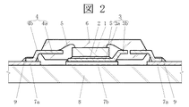
【解決手段】 タブの半導体チップ搭載領域に搭載した半導体チップと、このタブの周囲に配置され封止体外に露出して外部端子となるリードとを電気的に接続した半導体装置において、前記タブのボンディング領域と半導体チップの電源回路用のパッドとを電気的に接続し、前記タブの一部を前記封止体外に露出させ、このタブの露出部分を半導体装置の電源用外部端子とする。
タブの露出部分を接地電源用外部端子として用いるため、リードを外部端子として用いていた従来の半導体装置と比較して、伝送経路が短縮され、その断面積が増加するため、低インダクタンス・低インピーダンス化を図ることが可能となる。
【選択図】 図2
Description
こうした底面端子型の半導体装置については、下記特許文献に開示されている。
本発明の前記ならびにその他の課題と新規な特徴は、本明細書の記述及び添付図面から明らかになるであろう。
タブの露出部分を接地電源用外部端子として用いるため、リードを外部端子として用いていた従来の半導体装置と比較して、伝送経路が短縮され、その断面積が増加するため、低インダクタンス・低インピーダンス化を図ることが可能となる。なお、従来の半導体装置にも、半導体チップを搭載するタブを封止体から露出させているものがあるが、それらの半導体装置ではタブを放熱板としても利用しているに過ぎず、単に放熱性を考慮しているに留まり、高周波特性の点は考慮されていない。
(1)本発明によれば、伝送経路が短縮され、その断面積が増加するため、接地伝送経路の低インダクタンス・低抵抗化を図ることが可能となるという効果がある。
(2)本発明によれば、ボンディングワイヤの短縮によって低インピーダンス化を図ることが可能となるという効果がある。
(3)本発明によれば、上記効果(1)(2)により、アイソレーション特性が向上するという効果がある。
(4)本発明によれば、上記効果(2)(1)により、RF特性が格段に向上するという効果がある。
なお、実施の形態を説明するための全図において、同一機能を有するものは同一符号を付け、その繰り返しの説明は省略する。
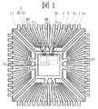
図1は本発明の一実施の形態であるQFP型半導体装置を封止体を透過して示す平面図であり、図1中のa‐a線に沿った縦断面図を基板実装状態として図2に示してある。
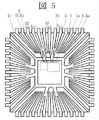
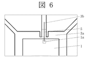
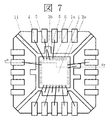
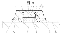
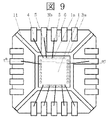
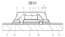
図7は本発明の他の実施の形態であるQFN型半導体装置を封止体を透過して示す平面図であり、図7中のa‐a線に沿った縦断面図を基板実装状態として図8に示してある。
Claims (2)
- タブの半導体チップ搭載領域に搭載した半導体チップと、このタブの周囲に配置され封止体外に露出して外部端子となる複数のリードとを電気的に接続した半導体装置において、
前記複数のリードの一部は前記タブに接続一体化され、前記タブに接続一体化されたリードの裏面側は部分的にエッチングされた構造であり、
前記半導体チップの接地電源用のパッドと前記タブに接続一体化されたリードの表面側とが電気的に接続され、前記タブの底面を前記封止体の底面から露出させ、この露出しているタブの底面を半導体装置の接地電源用外部端子としたことを特徴とする半導体装置。 - 前記半導体チップの接地電源用のパッドに接続される部分のリードと前記タブとの間が前記の部分的にエッチングされた構造であることを特徴とする請求項1に記載の半導体装置。
Priority Applications (1)
| Application Number | Priority Date | Filing Date | Title |
|---|---|---|---|
| JP2005195940A JP4252563B2 (ja) | 2005-07-05 | 2005-07-05 | 半導体装置 |
Applications Claiming Priority (1)
| Application Number | Priority Date | Filing Date | Title |
|---|---|---|---|
| JP2005195940A JP4252563B2 (ja) | 2005-07-05 | 2005-07-05 | 半導体装置 |
Related Parent Applications (1)
| Application Number | Title | Priority Date | Filing Date |
|---|---|---|---|
| JP2000296380A Division JP2002110889A (ja) | 2000-09-28 | 2000-09-28 | 半導体装置及びその製造方法 |
Publications (2)
| Publication Number | Publication Date |
|---|---|
| JP2005294871A true JP2005294871A (ja) | 2005-10-20 |
| JP4252563B2 JP4252563B2 (ja) | 2009-04-08 |
Family
ID=35327379
Family Applications (1)
| Application Number | Title | Priority Date | Filing Date |
|---|---|---|---|
| JP2005195940A Expired - Fee Related JP4252563B2 (ja) | 2005-07-05 | 2005-07-05 | 半導体装置 |
Country Status (1)
| Country | Link |
|---|---|
| JP (1) | JP4252563B2 (ja) |
Cited By (4)
| Publication number | Priority date | Publication date | Assignee | Title |
|---|---|---|---|---|
| JP2009060093A (ja) * | 2007-08-06 | 2009-03-19 | Seiko Instruments Inc | 半導体装置 |
| KR100939153B1 (ko) | 2007-12-11 | 2010-01-28 | 주식회사 하이닉스반도체 | 반도체 소자 및 그 제조 방법 |
| JP2012227347A (ja) * | 2011-04-19 | 2012-11-15 | Toyota Central R&D Labs Inc | 高周波装置 |
| JP2013508974A (ja) * | 2009-10-19 | 2013-03-07 | ナショナル セミコンダクター コーポレーション | 向上した接地ボンド信頼性を有するリードフレーム・パッケージ |
Citations (4)
| Publication number | Priority date | Publication date | Assignee | Title |
|---|---|---|---|---|
| JPH05291483A (ja) * | 1992-04-10 | 1993-11-05 | Toshiba Corp | 半導体装置 |
| JPH1174404A (ja) * | 1997-08-28 | 1999-03-16 | Nec Corp | ボールグリッドアレイ型半導体装置 |
| JPH11233683A (ja) * | 1998-02-10 | 1999-08-27 | Dainippon Printing Co Ltd | 樹脂封止型半導体装置とそれに用いられる回路部材および樹脂封止型半導体装置の製造方法 |
| JPH11260990A (ja) * | 1998-03-12 | 1999-09-24 | Matsushita Electron Corp | リードフレーム,樹脂封止型半導体装置及びその製造方法 |
-
2005
- 2005-07-05 JP JP2005195940A patent/JP4252563B2/ja not_active Expired - Fee Related
Patent Citations (4)
| Publication number | Priority date | Publication date | Assignee | Title |
|---|---|---|---|---|
| JPH05291483A (ja) * | 1992-04-10 | 1993-11-05 | Toshiba Corp | 半導体装置 |
| JPH1174404A (ja) * | 1997-08-28 | 1999-03-16 | Nec Corp | ボールグリッドアレイ型半導体装置 |
| JPH11233683A (ja) * | 1998-02-10 | 1999-08-27 | Dainippon Printing Co Ltd | 樹脂封止型半導体装置とそれに用いられる回路部材および樹脂封止型半導体装置の製造方法 |
| JPH11260990A (ja) * | 1998-03-12 | 1999-09-24 | Matsushita Electron Corp | リードフレーム,樹脂封止型半導体装置及びその製造方法 |
Cited By (4)
| Publication number | Priority date | Publication date | Assignee | Title |
|---|---|---|---|---|
| JP2009060093A (ja) * | 2007-08-06 | 2009-03-19 | Seiko Instruments Inc | 半導体装置 |
| KR100939153B1 (ko) | 2007-12-11 | 2010-01-28 | 주식회사 하이닉스반도체 | 반도체 소자 및 그 제조 방법 |
| JP2013508974A (ja) * | 2009-10-19 | 2013-03-07 | ナショナル セミコンダクター コーポレーション | 向上した接地ボンド信頼性を有するリードフレーム・パッケージ |
| JP2012227347A (ja) * | 2011-04-19 | 2012-11-15 | Toyota Central R&D Labs Inc | 高周波装置 |
Also Published As
| Publication number | Publication date |
|---|---|
| JP4252563B2 (ja) | 2009-04-08 |
Similar Documents
| Publication | Publication Date | Title |
|---|---|---|
| CN101207117B (zh) | 系统级封装体及其制造方法 | |
| US6703696B2 (en) | Semiconductor package | |
| CN100416815C (zh) | 包括无源器件的引线框架及其形成方法 | |
| JP2001313363A (ja) | 樹脂封止型半導体装置 | |
| KR100369907B1 (ko) | 반도체 패키지와 그 반도체 패키지의 기판 실장 구조 및적층 구조 | |
| JPH09312375A (ja) | リードフレーム、半導体装置及び半導体装置の製造方法 | |
| CN100463169C (zh) | 混合集成电路装置及其制造方法 | |
| US7875968B2 (en) | Leadframe, semiconductor package and support lead for bonding with groundwires | |
| JP2000294715A (ja) | 半導体装置及び半導体装置の製造方法 | |
| JP3839178B2 (ja) | 半導体装置 | |
| US6774464B2 (en) | Semiconductor device and method of manufacturing the same | |
| US7102211B2 (en) | Semiconductor device and hybrid integrated circuit device | |
| CN114068468A (zh) | 引线框架及封装结构 | |
| JP2004349397A (ja) | 半導体装置およびそれに用いられるリードフレーム | |
| KR100248035B1 (ko) | 반도체 패키지 | |
| JP4252563B2 (ja) | 半導体装置 | |
| US20040159929A1 (en) | Semiconductor die package having two die paddles | |
| JP4652281B2 (ja) | 樹脂封止型半導体装置 | |
| JP2002110889A (ja) | 半導体装置及びその製造方法 | |
| JP2005191158A (ja) | 半導体装置及びその製造方法 | |
| JP3913228B2 (ja) | 樹脂封止型半導体装置及びその製造方法 | |
| JP2006222471A5 (ja) | ||
| CN218632028U (zh) | 半导体封装结构 | |
| JPH11340405A (ja) | リードフレーム、半導体装置およびその製造方法 | |
| JP5145596B2 (ja) | 半導体装置 |
Legal Events
| Date | Code | Title | Description |
|---|---|---|---|
| A977 | Report on retrieval |
Free format text: JAPANESE INTERMEDIATE CODE: A971007 Effective date: 20070411 |
|
| A131 | Notification of reasons for refusal |
Free format text: JAPANESE INTERMEDIATE CODE: A131 Effective date: 20080610 |
|
| A521 | Request for written amendment filed |
Free format text: JAPANESE INTERMEDIATE CODE: A523 Effective date: 20080808 |
|
| A131 | Notification of reasons for refusal |
Free format text: JAPANESE INTERMEDIATE CODE: A131 Effective date: 20080930 |
|
| A521 | Request for written amendment filed |
Free format text: JAPANESE INTERMEDIATE CODE: A523 Effective date: 20081128 |
|
| TRDD | Decision of grant or rejection written | ||
| A01 | Written decision to grant a patent or to grant a registration (utility model) |
Free format text: JAPANESE INTERMEDIATE CODE: A01 Effective date: 20090120 |
|
| A01 | Written decision to grant a patent or to grant a registration (utility model) |
Free format text: JAPANESE INTERMEDIATE CODE: A01 |
|
| A61 | First payment of annual fees (during grant procedure) |
Free format text: JAPANESE INTERMEDIATE CODE: A61 Effective date: 20090121 |
|
| R150 | Certificate of patent or registration of utility model |
Free format text: JAPANESE INTERMEDIATE CODE: R150 |
|
| FPAY | Renewal fee payment (event date is renewal date of database) |
Free format text: PAYMENT UNTIL: 20120130 Year of fee payment: 3 |
|
| FPAY | Renewal fee payment (event date is renewal date of database) |
Free format text: PAYMENT UNTIL: 20120130 Year of fee payment: 3 |
|
| S111 | Request for change of ownership or part of ownership |
Free format text: JAPANESE INTERMEDIATE CODE: R313111 |
|
| FPAY | Renewal fee payment (event date is renewal date of database) |
Free format text: PAYMENT UNTIL: 20120130 Year of fee payment: 3 |
|
| R350 | Written notification of registration of transfer |
Free format text: JAPANESE INTERMEDIATE CODE: R350 |
|
| FPAY | Renewal fee payment (event date is renewal date of database) |
Free format text: PAYMENT UNTIL: 20130130 Year of fee payment: 4 |
|
| FPAY | Renewal fee payment (event date is renewal date of database) |
Free format text: PAYMENT UNTIL: 20130130 Year of fee payment: 4 |
|
| FPAY | Renewal fee payment (event date is renewal date of database) |
Free format text: PAYMENT UNTIL: 20140130 Year of fee payment: 5 |
|
| S531 | Written request for registration of change of domicile |
Free format text: JAPANESE INTERMEDIATE CODE: R313531 |
|
| R350 | Written notification of registration of transfer |
Free format text: JAPANESE INTERMEDIATE CODE: R350 |
|
| LAPS | Cancellation because of no payment of annual fees |