JP2005294871A - Semiconductor device - Google Patents
Semiconductor device Download PDFInfo
- Publication number
- JP2005294871A JP2005294871A JP2005195940A JP2005195940A JP2005294871A JP 2005294871 A JP2005294871 A JP 2005294871A JP 2005195940 A JP2005195940 A JP 2005195940A JP 2005195940 A JP2005195940 A JP 2005195940A JP 2005294871 A JP2005294871 A JP 2005294871A
- Authority
- JP
- Japan
- Prior art keywords
- tab
- semiconductor chip
- semiconductor device
- lead
- sealing body
- Prior art date
- Legal status (The legal status is an assumption and is not a legal conclusion. Google has not performed a legal analysis and makes no representation as to the accuracy of the status listed.)
- Granted
Links
Images


Classifications
-
- H—ELECTRICITY
- H10—SEMICONDUCTOR DEVICES; ELECTRIC SOLID-STATE DEVICES NOT OTHERWISE PROVIDED FOR
- H10W—GENERIC PACKAGES, INTERCONNECTIONS, CONNECTORS OR OTHER CONSTRUCTIONAL DETAILS OF DEVICES COVERED BY CLASS H10
- H10W72/00—Interconnections or connectors in packages
- H10W72/851—Dispositions of multiple connectors or interconnections
- H10W72/874—On different surfaces
- H10W72/884—Die-attach connectors and bond wires
-
- H—ELECTRICITY
- H10—SEMICONDUCTOR DEVICES; ELECTRIC SOLID-STATE DEVICES NOT OTHERWISE PROVIDED FOR
- H10W—GENERIC PACKAGES, INTERCONNECTIONS, CONNECTORS OR OTHER CONSTRUCTIONAL DETAILS OF DEVICES COVERED BY CLASS H10
- H10W72/00—Interconnections or connectors in packages
- H10W72/90—Bond pads, in general
- H10W72/931—Shapes of bond pads
- H10W72/932—Plan-view shape, i.e. in top view
-
- H—ELECTRICITY
- H10—SEMICONDUCTOR DEVICES; ELECTRIC SOLID-STATE DEVICES NOT OTHERWISE PROVIDED FOR
- H10W—GENERIC PACKAGES, INTERCONNECTIONS, CONNECTORS OR OTHER CONSTRUCTIONAL DETAILS OF DEVICES COVERED BY CLASS H10
- H10W74/00—Encapsulations, e.g. protective coatings
-
- H—ELECTRICITY
- H10—SEMICONDUCTOR DEVICES; ELECTRIC SOLID-STATE DEVICES NOT OTHERWISE PROVIDED FOR
- H10W—GENERIC PACKAGES, INTERCONNECTIONS, CONNECTORS OR OTHER CONSTRUCTIONAL DETAILS OF DEVICES COVERED BY CLASS H10
- H10W90/00—Package configurations
- H10W90/701—Package configurations characterised by the relative positions of pads or connectors relative to package parts
- H10W90/731—Package configurations characterised by the relative positions of pads or connectors relative to package parts of die-attach connectors
- H10W90/736—Package configurations characterised by the relative positions of pads or connectors relative to package parts of die-attach connectors between a chip and a stacked lead frame, conducting package substrate or heat sink
-
- H—ELECTRICITY
- H10—SEMICONDUCTOR DEVICES; ELECTRIC SOLID-STATE DEVICES NOT OTHERWISE PROVIDED FOR
- H10W—GENERIC PACKAGES, INTERCONNECTIONS, CONNECTORS OR OTHER CONSTRUCTIONAL DETAILS OF DEVICES COVERED BY CLASS H10
- H10W90/00—Package configurations
- H10W90/701—Package configurations characterised by the relative positions of pads or connectors relative to package parts
- H10W90/751—Package configurations characterised by the relative positions of pads or connectors relative to package parts of bond wires
- H10W90/756—Package configurations characterised by the relative positions of pads or connectors relative to package parts of bond wires between a chip and a stacked lead frame, conducting package substrate or heat sink
Landscapes
- Lead Frames For Integrated Circuits (AREA)
Abstract
【課題】 接地インダクタンスを低減し、高周波特性の良好なパッケージング技術を提供する。
【解決手段】 タブの半導体チップ搭載領域に搭載した半導体チップと、このタブの周囲に配置され封止体外に露出して外部端子となるリードとを電気的に接続した半導体装置において、前記タブのボンディング領域と半導体チップの電源回路用のパッドとを電気的に接続し、前記タブの一部を前記封止体外に露出させ、このタブの露出部分を半導体装置の電源用外部端子とする。
タブの露出部分を接地電源用外部端子として用いるため、リードを外部端子として用いていた従来の半導体装置と比較して、伝送経路が短縮され、その断面積が増加するため、低インダクタンス・低インピーダンス化を図ることが可能となる。
【選択図】 図2
PROBLEM TO BE SOLVED: To provide a packaging technique that reduces ground inductance and has good high frequency characteristics.
In a semiconductor device in which a semiconductor chip mounted in a semiconductor chip mounting region of a tab is electrically connected to a lead disposed around the tab and exposed to the outside of a sealing body to serve as an external terminal. The bonding region and the power supply circuit pad of the semiconductor chip are electrically connected, a part of the tab is exposed to the outside of the sealing body, and the exposed part of the tab is used as a power supply external terminal of the semiconductor device.
Because the exposed part of the tab is used as an external terminal for ground power supply, the transmission path is shortened and its cross-sectional area is increased compared to conventional semiconductor devices that use leads as external terminals. Can be achieved.
[Selection] Figure 2
Description
本発明は、半導体装置及びその製造方法に関し、特に、半導体装置の高周波特性の向上に適用して有効な技術に関するものである。 The present invention relates to a semiconductor device and a manufacturing method thereof, and more particularly to a technique effective when applied to improvement of high-frequency characteristics of a semiconductor device.
半導体装置として、製造が比較的容易で低コストであることから、樹脂を用いた封止体によって半導体チップを覆い、封止体から延在するリードを外部端子とするSOP型、SOJ型或いはQFP型等の半導体装置が広く用いられている。 As a semiconductor device, since it is relatively easy to manufacture and low cost, an SOP type, SOJ type, or QFP in which a semiconductor chip is covered with a sealing body using a resin and leads extending from the sealing body are external terminals. Semiconductor devices such as molds are widely used.
これらQFP型等の半導体装置では、半導体装置の外部端子となるリードが封止体側面から延在しているために、実装状態では、リードと配線基板との接続領域が半導体装置の周囲に必要となる。このため、半導体装置周囲の前記接続領域の面積を縮小して電子装置を小型化するために、前記封止体の底面外周部にてリード底面を封止体から露出させて半導体装置の外部端子とする底面端子型の半導体装置が考えられた。底面端子型の半導体装置としては、QFN(Quad Flat Nonlead)型或いはSON(Small Outline Nonlead)型等の半導体装置が知られている。 In these QFP type semiconductor devices, since the leads serving as the external terminals of the semiconductor device extend from the side surface of the sealing body, a connection region between the leads and the wiring board is required around the semiconductor device in the mounted state. It becomes. For this reason, in order to reduce the area of the connection region around the semiconductor device and reduce the size of the electronic device, the bottom surface of the lead is exposed from the sealing body at the outer periphery of the bottom surface of the sealing body, and the external terminal of the semiconductor device A bottom terminal type semiconductor device is considered. As the bottom terminal type semiconductor device, a semiconductor device of QFN (Quad Flat Nonlead) type or SON (Small Outline Nonlead) type is known.
また、前述したQFP型或いはQFN型等の半導体装置の組立てにはリードフレームが用いられており、半導体チップをレジン又は銀ペーストによってタブに固定し、半導体チップのパッドとリードとがボンディングワイヤによって電気的に接続されている。このボンディング後に、半導体チップ、タブ、ボンディングワイヤが例えばエポキシ樹脂からなる封止体によって封止され、ダムバー及びタイバーが切断されて各リードは機械的・電気的に分離され、分離されたリードを所定形状に成形して、半導体装置が完成する。
こうした底面端子型の半導体装置については、下記特許文献に開示されている。
Further, a lead frame is used for assembling the above-described semiconductor devices such as the QFP type or the QFN type, and the semiconductor chip is fixed to the tab with resin or silver paste, and the pads and leads of the semiconductor chip are electrically connected by bonding wires. Connected. After this bonding, the semiconductor chip, the tab, and the bonding wire are sealed with a sealing body made of, for example, epoxy resin, the dam bar and the tie bar are cut, and the respective leads are mechanically and electrically separated. The semiconductor device is completed by forming into a shape.
Such a bottom terminal type semiconductor device is disclosed in the following patent document.
半導体装置では、携帯電話等の移動体通信に代表されるように、播送される情報量の飛躍的な増加によって高速通信網の整備が必須となり、使用周波数の高速化が進められ、このような高周波信号を処理するための半導体装置には高周波RF特性の向上が求められている。このため、高周波信号を処理する半導体チップを搭載した半導体装置では、パッケージングの技術についても、半導体チップと実装基板との伝送系となるリード等にも高周波特性を活かした構造とすることが求められ、接地インダクタンスを低減することが必要となっている。 In semiconductor devices, as typified by mobile communications such as mobile phones, it is essential to develop a high-speed communication network due to a dramatic increase in the amount of information to be transmitted, and the use frequency is increased. Semiconductor devices for processing high-frequency signals are required to improve high-frequency RF characteristics. For this reason, semiconductor devices equipped with semiconductor chips that process high-frequency signals are required to have a structure that utilizes high-frequency characteristics in packaging technology and leads that serve as a transmission system between the semiconductor chip and the mounting substrate. Therefore, it is necessary to reduce the ground inductance.
本発明の課題は、接地インダクタンスを低減し、高周波特性の良好なパッケージング技術を提供することにある。
本発明の前記ならびにその他の課題と新規な特徴は、本明細書の記述及び添付図面から明らかになるであろう。
An object of the present invention is to provide a packaging technique that reduces ground inductance and has good high-frequency characteristics.
The above and other problems and novel features of the present invention will be apparent from the description of this specification and the accompanying drawings.
本願において開示される発明のうち、代表的なものの概要を簡単に説明すれば下記の通りである。 Of the inventions disclosed in this application, the outline of typical ones will be briefly described as follows.
タブの半導体チップ搭載領域に搭載した半導体チップと、このタブの周囲に配置され封止体外に露出して外部端子となるリードとを電気的に接続した半導体装置において、前記タブのボンディング領域と半導体チップの電源回路用のパッドとを電気的に接続し、前記タブの一部を前記封止体外に露出させ、このタブの露出部分を半導体装置の電源用外部端子とする。 In a semiconductor device in which a semiconductor chip mounted in a semiconductor chip mounting region of a tab and a lead that is arranged around the tab and is exposed outside the sealing body to be an external terminal are electrically connected, the bonding region of the tab and the semiconductor A pad for a power supply circuit of the chip is electrically connected, a part of the tab is exposed outside the sealing body, and the exposed part of the tab is used as an external terminal for power supply of the semiconductor device.
また、タブの半導体チップ搭載領域に搭載した半導体チップと、このタブの周囲に配置され封止体外に露出して外部端子となるリードとを電気的に接続した半導体装置において、前記タブのボンディング領域と半導体チップの接地電源用のパッドとを電気的に接続し、前記タブの底面を前記封止体の底面から露出させ、この露出しているタブの底面を半導体装置の接地電源用外部端子とする。 Further, in the semiconductor device in which the semiconductor chip mounted in the semiconductor chip mounting region of the tab and the leads that are arranged around the tab and are exposed outside the sealing body to be external terminals are electrically connected, the bonding region of the tab Are electrically connected to the ground power supply pad of the semiconductor chip, the bottom surface of the tab is exposed from the bottom surface of the sealing body, and the exposed bottom surface of the tab is connected to the ground power supply external terminal of the semiconductor device. To do.
更に、タブの半導体チップ搭載領域に搭載した半導体チップと、このタブの周囲に配置され封止体外に露出して外部端子となるリードとを電気的に接続する半導体装置の製造方法において、タブの半導体チップ搭載領域に半導体チップを搭載する工程と、前記半導体チップのパッドとリードとをボンディングし、前記半導体チップの接地電源用のパッドとタブのボンディング領域とをボンディングする工程と、前記タブの底面を露出させて封止体を形成する工程とを有する。 Further, in a method of manufacturing a semiconductor device in which a semiconductor chip mounted in a semiconductor chip mounting region of a tab and a lead disposed around the tab and exposed to the outside of the sealing body to be an external terminal are electrically connected. Mounting a semiconductor chip in a semiconductor chip mounting region, bonding a pad and a lead of the semiconductor chip, bonding a ground power supply pad of the semiconductor chip and a bonding region of a tab, and a bottom surface of the tab And a step of forming a sealing body.
(作用)
タブの露出部分を接地電源用外部端子として用いるため、リードを外部端子として用いていた従来の半導体装置と比較して、伝送経路が短縮され、その断面積が増加するため、低インダクタンス・低インピーダンス化を図ることが可能となる。なお、従来の半導体装置にも、半導体チップを搭載するタブを封止体から露出させているものがあるが、それらの半導体装置ではタブを放熱板としても利用しているに過ぎず、単に放熱性を考慮しているに留まり、高周波特性の点は考慮されていない。
(Function)
Because the exposed part of the tab is used as an external terminal for ground power supply, the transmission path is shortened and its cross-sectional area is increased compared to conventional semiconductor devices that use leads as external terminals. Can be achieved. Note that some conventional semiconductor devices have a tab on which a semiconductor chip is mounted exposed from a sealing body, but these semiconductor devices only use the tab as a heat sink, and simply dissipate heat. However, high frequency characteristics are not taken into consideration.
本願において開示される発明のうち代表的なものによって得られる効果を簡単に説明すれば、下記の通りである。
(1)本発明によれば、伝送経路が短縮され、その断面積が増加するため、接地伝送経路の低インダクタンス・低抵抗化を図ることが可能となるという効果がある。
(2)本発明によれば、ボンディングワイヤの短縮によって低インピーダンス化を図ることが可能となるという効果がある。
(3)本発明によれば、上記効果(1)(2)により、アイソレーション特性が向上するという効果がある。
(4)本発明によれば、上記効果(2)(1)により、RF特性が格段に向上するという効果がある。
The effects obtained by the representative ones of the inventions disclosed in the present application will be briefly described as follows.
(1) According to the present invention, since the transmission path is shortened and the cross-sectional area thereof is increased, it is possible to reduce the inductance and resistance of the ground transmission path.
(2) According to the present invention, it is possible to reduce the impedance by shortening the bonding wire.
(3) According to the present invention, the effects (1) and (2) have the effect of improving the isolation characteristics.
(4) According to the present invention, there is an effect that the RF characteristics are remarkably improved by the effects (2) and (1).
以下、本発明の実施の形態を説明する。
なお、実施の形態を説明するための全図において、同一機能を有するものは同一符号を付け、その繰り返しの説明は省略する。
Embodiments of the present invention will be described below.
Note that components having the same function are denoted by the same reference symbols throughout the drawings for describing the embodiment, and the repetitive description thereof will be omitted.
(実施の形態1)
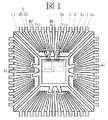
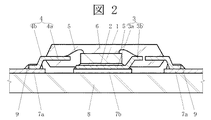
図1は本発明の一実施の形態であるQFP型半導体装置を封止体を透過して示す平面図であり、図1中のa‐a線に沿った縦断面図を基板実装状態として図2に示してある。
(Embodiment 1)
FIG. 1 is a plan view showing a QFP-type semiconductor device according to an embodiment of the present invention through a sealing body, and a longitudinal sectional view taken along the line aa in FIG. This is shown in FIG.
本実施の形態の半導体装置では、単結晶シリコン等の半導体基板に所定の素子を形成した半導体チップ1を、レジン又は銀ペースト等の接合剤2によってタブ3の半導体チップ搭載領域3aに固定し、半導体チップ1のパッド1aとリード4のインナーリード4aの内端とをボンディングワイヤ5によって電気的に接続してある。半導体チップ1の電源回路の接地用パッド1aは接地用のリード4と接続するが、並列して接地用のパッド1aとタブ3のボンディング領域3bとをボンディングワイヤ5によって接続する。
In the semiconductor device of the present embodiment, the
半導体チップ1、タブ3、リード4のインナーリード4a、ボンディングワイヤ5は、例えばエポキシ樹脂にフィラを混入させた封止樹脂を用いた封止体6によってタブ3の一部である底面を露出させて封止する。リード4のアウターリード4bは、封止体6の側面から露出し、実装状態では、アウターリード4bの外端が配線基板に接続固定される。
The
配線基板は、配線層7がガラスエポキシ或いはムライトセラミック等の絶縁性材料を板状に成形した基体8の表面或いは内部に形成されており、最上層に形成された配線層7が部分的に、半導体装置の外部端子であるアウターリード4bとの接続端子7aとなっており、実装状態では、接続端子7aとアウターリード4bとを接合剤であるハンダ9によって接続する。そして、本実施の形態の半導体装置では、封止体6から露出しているタブ3の露出部分を半導体装置の接地電源用外部端子として用い、その底面を接地電位の配線層7の接続端子7bに接合剤であるハンダ9によって接続する。
In the wiring board, the wiring layer 7 is formed on the surface or inside of the
このように、タブ3の露出部分を接地電源用外部端子として用いるため、リード4を外部端子として用いていた従来の半導体装置と比較して、伝送経路が短縮され、その断面積が増加するため、接地伝送経路の低インダクタンス・低抵抗化を図ることが可能となり、ボンディングワイヤの短縮によって低インピーダンス化を図ることが可能となる。これによって、アイソレーション特性が向上し、RF特性が格段に向上する。
As described above, since the exposed portion of the
また、タブ3の露出部分を接地電源用外部端子として用いるので、電源供給の問題だけを考えた場合には、半導体チップ1の電源回路の接地用パッド1aを接地用のリードVccと接続しなくてもよい。しかし、接地用パッド1aと接続した接地用のリードVccを、高周波信号の入出力リードRFin,RFoutに隣接させて配置することによって、高周波信号を安定化させることができる利点がある。加えて、接地用のリードVccを設けておくことによって、従来の半導体装置のピン配置と互換性をもたせることが可能になる。これらの利点が必要とされない場合であれば、接地用のリードVccと半導体チップ1とをボンディング接続しない構成、更に接地用のリードVccを設けずに少ピン化する構成とすることも可能である。
In addition, since the exposed portion of the
ところで、封止体6の樹脂とタブ3或いはリード4の金属とでは、熱膨張係数に違いがある。フィラ等により調整して熱膨張係数を近付けたとしても、熱による収縮・膨張の過渡的な特性は変えることができず、この相違から収縮・膨張の速度が異なり、熱による収縮・膨張の際に前記樹脂と金属との界面にずれが生じる。こうしたずれは、半導体装置の中心から遠ざかるに連れて大きくなるため、タブ3の周縁に位置するボンディング領域3bでは、このずれによってボンディングワイヤ5に剪断応力が働き、ボンディングワイヤ5が外れて導通が絶たれてしまうことがある。こうした断線は単に電源供給の問題に留まらず、例えば高周波信号の配線と隣接して設けられた接地配線が断線した場合には、伝送される高周波信号に影響を与えることになる。
By the way, there is a difference in thermal expansion coefficient between the resin of the sealing
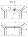
このような断線を防止するためには、図3に部分平面図を示し、図3中のa‐a線に沿った縦断面図を図4に示しているように、収縮前記タブのボンディング領域と半導体チップ搭載領域との間に孔或いはスリットからなる分離部10を設けることが有効である。この分離部10によって半導体チップ搭載領域3aとボンディング領域3bとが分断されているため、半導体チップ搭載領域3aの熱応力はボンディング領域3bには伝わりにくくなる。加えて、この分離部10に充填された樹脂によってタブ3の上下に位置する樹脂が一体化され、ボンディング領域3bは近傍の樹脂と挙動をともにすることとなり、樹脂とボンディング領域3bとの間に生じるずれが小さくなるため、ボンディングワイヤ5に大きな剪断応力が加えられることがなくなる。
In order to prevent such disconnection, as shown in FIG. 3, a partial plan view, and a longitudinal sectional view along the line aa in FIG. It is effective to provide a
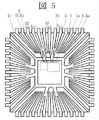
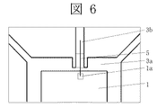
また、図5は本発明の一実施の形態の変形例を封止体を透過して示す平面図である。この例では、接地用のリード4をタブに直接接続して一体化してある。このため半導体チップ1とのボンディングを1本のボンディングワイヤで行なうことができる。この場合に、インナーリード4aがタブ3に近接しているために、ボンディング領域3bの段上げが難しくなることがある。こうした場合には、図6に部分平面図を示すようにタブ3に切り込みを設けて、この部分で段上げを行なう構成とすることが可能である。
FIG. 5 is a plan view showing a modified example of the embodiment of the present invention through a sealing body. In this example, the
続いて、本実施の形態の半導体装置の製造方法について説明する。本実施の形態の半導体装置は、個々の半導体装置に用いられるタブ及びリードの組がタイバー或いはダムバーによって一体化されたタブ及びリードの組が連続して複数組形成され、夫々のリードフレームを用いており、リードフレームとしては、例えばFe‐Ni系合金或いはCu系合金等からなり、半導体チップ1が搭載されるタブ3の全周囲にわたって複数の信号用のリード4が配置されており、タブ3はリード4の間に設けられたタブ吊りリード11によってタブ3をフレームに支持している。
Subsequently, a method for manufacturing the semiconductor device of the present embodiment will be described. In the semiconductor device of the present embodiment, a plurality of sets of tabs and leads in which a set of tabs and leads used for each semiconductor device is integrated by a tie bar or a dam bar are formed in succession, and each lead frame is used. The lead frame is made of, for example, Fe-Ni alloy or Cu alloy, and a plurality of signal leads 4 are arranged around the entire periphery of the
そして、このリードフレームの夫々のタブ3の半導体チップ搭載領域3aに夫々半導体チップ1をレジン又は銀ペーストによって固定し、半導体チップ1のパッド1a電極とインナーリード4aとをボンディングワイヤ5によって接続し、半導体チップ1をリードフレームに実装する。半導体チップ1とインナーリード4aとのボンディングの際に、半導体チップ1の接地電源用のパッド1aとタブ3のボンディング領域3bとをボンディングする。
Then, the
次に、半導体チップ1を実装したリードフレームを、金型のキャビデイ内に半導体チップ1、タブ3、リード4、ボンディングワイヤ5を収容して、封止樹脂を注入して封止体6を形成する。この時、タブ3の下面は金型に密着させているため、封止樹脂が付着せずに封止体6の底面にタブ3の底面が露出することとなる。この後、タイバー或いはダムバーを切断し、個々の半導体装置に分離して、アウターリード4bをガルウイング等に成形する。
Next, the
(実施の形態2)
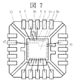
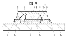
図7は本発明の他の実施の形態であるQFN型半導体装置を封止体を透過して示す平面図であり、図7中のa‐a線に沿った縦断面図を基板実装状態として図8に示してある。
(Embodiment 2)
FIG. 7 is a plan view showing a QFN type semiconductor device according to another embodiment of the present invention through a sealing body, and a longitudinal sectional view taken along line aa in FIG. It is shown in FIG.
本実施の形態の半導体装置では、単結晶シリコン等の半導体基板に所定の素子を形成した半導体チップ1を、レジン又は銀ペースト等の接合剤2によってタブ3の半導体チップ搭載領域3aに固定し、半導体チップ1のパッド1aとリード4のインナーリード4aの内端とをボンディングワイヤ5によって電気的に接続してある。半導体チップ1の電源回路の接地用パッド1aは接地用のリード4と接続するが、並列して接地用のパッド1aとタブ3のボンディング領域3bとをボンディングワイヤ5によって接続する。
In the semiconductor device of the present embodiment, the
半導体チップ1、タブ3、リード4の上面及び側面、ボンディングワイヤ5は、例えばエポキシ樹脂にフィラを混入させた封止樹脂を用いた封止体6によってタブ3の一部である底面及びリード4の底面を露出させて封止する。実装状態では、このリード4の底面が配線基板に接続固定される。こうした底面端子型の半導体装置では、半導体チップを封止する封止体の底面に夫々複数のリードが設けられているために、半導体装置を配線基板に実装する場合に、その周囲に接続領域を設ける必要がないため半導体装置の実装状態での占有面積が減少し、周囲のスペースを有効に利用することができるという利点がある。
The top surface and side surfaces of the
配線基板は、配線層7がガラスエポキシ或いはムライトセラミック等の絶縁性材料を板状に成形した基体8の表面或いは内部に形成されており、最上層に形成された配線層7が部分的に、半導体装置の外部端子であるリード4の底面との接続端子7aとなっており、実装状態では、接続端子7aとリード4の底面とを接合剤であるハンダ9によって接続する。そして、本実施の形態の半導体装置では、封止体6から露出しているタブ3の露出部分を半導体装置の接地電源用外部端子として用い、その底面を接地電位の配線層7の接続端子7bに接合剤であるハンダ9によって接続する。
In the wiring board, the wiring layer 7 is formed on the surface or inside of the
なお、ボンディング領域3bは、ハーフエッチングによってその底面側を除去し、この部分に封止体6が形成してある。これは、ボンディング領域3bの底面が露出していると、配線基板に実装する際にタブ3を接続するハンダ9が隣接するリード4を接続するハンダ9と一体化してしまうハンダブリッジが生じるのを防止するためである。
Note that the bottom surface side of the
このように、タブ3の露出部分を接地電源用外部端子として用いるため、リード4を外部端子として用いていた従来の半導体装置と比較して、伝送経路が短縮され、その断面積が増加するため、接地伝送経路の低インダクタンス・低抵抗化を図ることが可能となり、ボンディングワイヤの短縮によって低インピーダンス化を図ることが可能となる。これによって、アイソレーション特性が向上し、RF特性が格段に向上する。
As described above, since the exposed portion of the
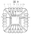
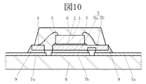
また、図9に封止体を透過して平面図を示し、図9中のa‐a線に沿った縦断面図を図10に示す本実施の形態の変形例では、接地用のリード4をタブに直接接続して一体化し、リード4の一部をボンディング領域3bとしている。このため半導体チップ1とのボンディングを1本のボンディングワイヤで行なうことができる。この場合に、タブ3とリード4との間をハーフエッチングしてあるが、この構成によって、前述したハンダブリッジを防止するとともに、前述した実施の形態の分離部10に相当する機能を発揮する。即ち、ハーフエッチングされた部分に充填された樹脂によってリード4の上に位置する樹脂がリード4と一体化されて近傍の樹脂と挙動をともにすることとなり、樹脂とリード4のボンディング領域3bとの間に生じるずれが小さくなるため、ボンディングワイヤ5に大きな剪断応力が加えられることがなくなる。
Further, FIG. 9 shows a plan view through the sealing body, and a longitudinal cross-sectional view along the aa line in FIG. Are directly connected to the tab and integrated, and a part of the
また本実施の形態は、図9に封止体を透過して平面図を示し、図9中のa‐a線に沿った縦断面図を図10に示す本実施の形態の変形例のように、通常のタブ3の周縁部をボンディング領域3bとして実施することもできる。従来のリードフレームをそのまま流用することも可能となり、本発明の実施が容易となる。
Further, in the present embodiment, a plan view is shown through FIG. 9 through the sealing body, and a longitudinal sectional view along the line aa in FIG. 9 is a modification of the present embodiment shown in FIG. In addition, the peripheral edge of the
以上、本発明者によってなされた発明を、前記実施の形態に基づき具体的に説明したが、本発明は、前記実施の形態に限定されるものではなく、その要旨を逸脱しない範囲において種々変更可能であることは勿論である。 Although the invention made by the present inventor has been specifically described based on the above-described embodiment, the present invention is not limited to the above-described embodiment, and various modifications can be made without departing from the scope of the invention. Of course.
例えば、以上の説明では、主として本発明者によってなされた発明をその背景となった利用分野であるQFP型或いはQFN型半導体装置に適用した場合について説明したが、それに限定されるものではなく、本発明は、他の形式の表面実装型半導体装置にも広く適用が可能である。 For example, in the above description, the case where the invention made mainly by the present inventor is applied to the QFP type or QFN type semiconductor device which is the field of use behind it has been described. However, the present invention is not limited to this. The invention can be widely applied to other types of surface-mount semiconductor devices.
1…半導体チップ、2…接合剤、3…タブ、3a…半導体チップ搭載領域、3b…ボンディング領域、4…リード、4a…インナーリード、4b…アウターリード、5…ボンディングワイヤ、6…封止体、7…配線層、8…基体、9…ハンダ、10…分離部、11…タブ吊りリード。
DESCRIPTION OF
Claims (2)
前記複数のリードの一部は前記タブに接続一体化され、前記タブに接続一体化されたリードの裏面側は部分的にエッチングされた構造であり、
前記半導体チップの接地電源用のパッドと前記タブに接続一体化されたリードの表面側とが電気的に接続され、前記タブの底面を前記封止体の底面から露出させ、この露出しているタブの底面を半導体装置の接地電源用外部端子としたことを特徴とする半導体装置。 In a semiconductor device in which a semiconductor chip mounted in a semiconductor chip mounting region of a tab and a plurality of leads which are arranged around the tab and are exposed to the outside of the sealing body to serve as external terminals are electrically connected,
A part of the plurality of leads is connected and integrated with the tab, and the back side of the lead connected and integrated with the tab has a partially etched structure,
The pad for ground power supply of the semiconductor chip and the surface side of the lead connected and integrated with the tab are electrically connected, and the bottom surface of the tab is exposed from the bottom surface of the sealing body. A semiconductor device characterized in that the bottom surface of the tab is an external terminal for grounding power of the semiconductor device.
Priority Applications (1)
| Application Number | Priority Date | Filing Date | Title |
|---|---|---|---|
| JP2005195940A JP4252563B2 (en) | 2005-07-05 | 2005-07-05 | Semiconductor device |
Applications Claiming Priority (1)
| Application Number | Priority Date | Filing Date | Title |
|---|---|---|---|
| JP2005195940A JP4252563B2 (en) | 2005-07-05 | 2005-07-05 | Semiconductor device |
Related Parent Applications (1)
| Application Number | Title | Priority Date | Filing Date |
|---|---|---|---|
| JP2000296380A Division JP2002110889A (en) | 2000-09-28 | 2000-09-28 | Semiconductor device and manufacturing method thereof |
Publications (2)
| Publication Number | Publication Date |
|---|---|
| JP2005294871A true JP2005294871A (en) | 2005-10-20 |
| JP4252563B2 JP4252563B2 (en) | 2009-04-08 |
Family
ID=35327379
Family Applications (1)
| Application Number | Title | Priority Date | Filing Date |
|---|---|---|---|
| JP2005195940A Expired - Fee Related JP4252563B2 (en) | 2005-07-05 | 2005-07-05 | Semiconductor device |
Country Status (1)
| Country | Link |
|---|---|
| JP (1) | JP4252563B2 (en) |
Cited By (4)
| Publication number | Priority date | Publication date | Assignee | Title |
|---|---|---|---|---|
| JP2009060093A (en) * | 2007-08-06 | 2009-03-19 | Seiko Instruments Inc | Semiconductor device |
| KR100939153B1 (en) | 2007-12-11 | 2010-01-28 | 주식회사 하이닉스반도체 | Semiconductor device and manufacturing method thereof |
| JP2012227347A (en) * | 2011-04-19 | 2012-11-15 | Toyota Central R&D Labs Inc | High frequency device |
| JP2013508974A (en) * | 2009-10-19 | 2013-03-07 | ナショナル セミコンダクター コーポレーション | Leadframe package with improved ground bond reliability |
Citations (4)
| Publication number | Priority date | Publication date | Assignee | Title |
|---|---|---|---|---|
| JPH05291483A (en) * | 1992-04-10 | 1993-11-05 | Toshiba Corp | Semiconductor device |
| JPH1174404A (en) * | 1997-08-28 | 1999-03-16 | Nec Corp | Ball grid array type semiconductor device |
| JPH11233683A (en) * | 1998-02-10 | 1999-08-27 | Dainippon Printing Co Ltd | Resin-sealed semiconductor device, circuit member used therefor, and method of manufacturing resin-sealed semiconductor device |
| JPH11260990A (en) * | 1998-03-12 | 1999-09-24 | Matsushita Electron Corp | Lead frame, resin-encapsulated semiconductor device and method of manufacturing the same |
-
2005
- 2005-07-05 JP JP2005195940A patent/JP4252563B2/en not_active Expired - Fee Related
Patent Citations (4)
| Publication number | Priority date | Publication date | Assignee | Title |
|---|---|---|---|---|
| JPH05291483A (en) * | 1992-04-10 | 1993-11-05 | Toshiba Corp | Semiconductor device |
| JPH1174404A (en) * | 1997-08-28 | 1999-03-16 | Nec Corp | Ball grid array type semiconductor device |
| JPH11233683A (en) * | 1998-02-10 | 1999-08-27 | Dainippon Printing Co Ltd | Resin-sealed semiconductor device, circuit member used therefor, and method of manufacturing resin-sealed semiconductor device |
| JPH11260990A (en) * | 1998-03-12 | 1999-09-24 | Matsushita Electron Corp | Lead frame, resin-encapsulated semiconductor device and method of manufacturing the same |
Cited By (4)
| Publication number | Priority date | Publication date | Assignee | Title |
|---|---|---|---|---|
| JP2009060093A (en) * | 2007-08-06 | 2009-03-19 | Seiko Instruments Inc | Semiconductor device |
| KR100939153B1 (en) | 2007-12-11 | 2010-01-28 | 주식회사 하이닉스반도체 | Semiconductor device and manufacturing method thereof |
| JP2013508974A (en) * | 2009-10-19 | 2013-03-07 | ナショナル セミコンダクター コーポレーション | Leadframe package with improved ground bond reliability |
| JP2012227347A (en) * | 2011-04-19 | 2012-11-15 | Toyota Central R&D Labs Inc | High frequency device |
Also Published As
| Publication number | Publication date |
|---|---|
| JP4252563B2 (en) | 2009-04-08 |
Similar Documents
| Publication | Publication Date | Title |
|---|---|---|
| CN101207117B (en) | System-in-package and method of manufacturing the same | |
| US6703696B2 (en) | Semiconductor package | |
| CN100416815C (en) | Lead frame including passive devices and method of forming same | |
| JP2001313363A (en) | Resin-sealed semiconductor device | |
| KR100369907B1 (en) | Semiconductor Package And Mounting Structure On Substrate Thereof And Stack Structure Thereof | |
| JPH09312375A (en) | Lead frame, semiconductor device, and method of manufacturing semiconductor device | |
| CN100463169C (en) | Hybrid integrated circuit device and manufacturing method thereof | |
| US7875968B2 (en) | Leadframe, semiconductor package and support lead for bonding with groundwires | |
| JP2000294715A (en) | Semiconductor device and method of manufacturing semiconductor device | |
| JP3839178B2 (en) | Semiconductor device | |
| US6774464B2 (en) | Semiconductor device and method of manufacturing the same | |
| US7102211B2 (en) | Semiconductor device and hybrid integrated circuit device | |
| CN114068468A (en) | Lead frame and packaging structure | |
| JP2004349397A (en) | Semiconductor device and lead frame used therein | |
| KR100248035B1 (en) | Semiconductor package | |
| JP4252563B2 (en) | Semiconductor device | |
| US20040159929A1 (en) | Semiconductor die package having two die paddles | |
| JP4652281B2 (en) | Resin-sealed semiconductor device | |
| JP2002110889A (en) | Semiconductor device and manufacturing method thereof | |
| JP3913228B2 (en) | Resin-sealed semiconductor device and manufacturing method thereof | |
| JP2005191158A (en) | Semiconductor device and manufacturing method thereof | |
| JP2006222471A5 (en) | ||
| CN218632028U (en) | Semiconductor packaging structure | |
| JPH11340405A (en) | Lead frame, semiconductor device and method of manufacturing the same | |
| JP5145596B2 (en) | Semiconductor device |
Legal Events
| Date | Code | Title | Description |
|---|---|---|---|
| A977 | Report on retrieval |
Free format text: JAPANESE INTERMEDIATE CODE: A971007 Effective date: 20070411 |
|
| A131 | Notification of reasons for refusal |
Free format text: JAPANESE INTERMEDIATE CODE: A131 Effective date: 20080610 |
|
| A521 | Request for written amendment filed |
Free format text: JAPANESE INTERMEDIATE CODE: A523 Effective date: 20080808 |
|
| A131 | Notification of reasons for refusal |
Free format text: JAPANESE INTERMEDIATE CODE: A131 Effective date: 20080930 |
|
| A521 | Request for written amendment filed |
Free format text: JAPANESE INTERMEDIATE CODE: A523 Effective date: 20081128 |
|
| TRDD | Decision of grant or rejection written | ||
| A01 | Written decision to grant a patent or to grant a registration (utility model) |
Free format text: JAPANESE INTERMEDIATE CODE: A01 Effective date: 20090120 |
|
| A01 | Written decision to grant a patent or to grant a registration (utility model) |
Free format text: JAPANESE INTERMEDIATE CODE: A01 |
|
| A61 | First payment of annual fees (during grant procedure) |
Free format text: JAPANESE INTERMEDIATE CODE: A61 Effective date: 20090121 |
|
| R150 | Certificate of patent or registration of utility model |
Free format text: JAPANESE INTERMEDIATE CODE: R150 |
|
| FPAY | Renewal fee payment (event date is renewal date of database) |
Free format text: PAYMENT UNTIL: 20120130 Year of fee payment: 3 |
|
| FPAY | Renewal fee payment (event date is renewal date of database) |
Free format text: PAYMENT UNTIL: 20120130 Year of fee payment: 3 |
|
| S111 | Request for change of ownership or part of ownership |
Free format text: JAPANESE INTERMEDIATE CODE: R313111 |
|
| FPAY | Renewal fee payment (event date is renewal date of database) |
Free format text: PAYMENT UNTIL: 20120130 Year of fee payment: 3 |
|
| R350 | Written notification of registration of transfer |
Free format text: JAPANESE INTERMEDIATE CODE: R350 |
|
| FPAY | Renewal fee payment (event date is renewal date of database) |
Free format text: PAYMENT UNTIL: 20130130 Year of fee payment: 4 |
|
| FPAY | Renewal fee payment (event date is renewal date of database) |
Free format text: PAYMENT UNTIL: 20130130 Year of fee payment: 4 |
|
| FPAY | Renewal fee payment (event date is renewal date of database) |
Free format text: PAYMENT UNTIL: 20140130 Year of fee payment: 5 |
|
| S531 | Written request for registration of change of domicile |
Free format text: JAPANESE INTERMEDIATE CODE: R313531 |
|
| R350 | Written notification of registration of transfer |
Free format text: JAPANESE INTERMEDIATE CODE: R350 |
|
| LAPS | Cancellation because of no payment of annual fees |