JP2005294525A - 半導体装置の製造方法 - Google Patents
半導体装置の製造方法 Download PDFInfo
- Publication number
- JP2005294525A JP2005294525A JP2004107340A JP2004107340A JP2005294525A JP 2005294525 A JP2005294525 A JP 2005294525A JP 2004107340 A JP2004107340 A JP 2004107340A JP 2004107340 A JP2004107340 A JP 2004107340A JP 2005294525 A JP2005294525 A JP 2005294525A
- Authority
- JP
- Japan
- Prior art keywords
- insulating film
- film
- dielectric constant
- backfill
- wiring
- Prior art date
- Legal status (The legal status is an assumption and is not a legal conclusion. Google has not performed a legal analysis and makes no representation as to the accuracy of the status listed.)
- Pending
Links
Images


Classifications
-
- H—ELECTRICITY
- H10—SEMICONDUCTOR DEVICES; ELECTRIC SOLID-STATE DEVICES NOT OTHERWISE PROVIDED FOR
- H10W—GENERIC PACKAGES, INTERCONNECTIONS, CONNECTORS OR OTHER CONSTRUCTIONAL DETAILS OF DEVICES COVERED BY CLASS H10
- H10W20/00—Interconnections in chips, wafers or substrates
- H10W20/01—Manufacture or treatment
- H10W20/071—Manufacture or treatment of dielectric parts thereof
- H10W20/074—Manufacture or treatment of dielectric parts thereof of dielectric parts comprising thin functional dielectric layers, e.g. dielectric etch-stop, barrier, capping or liner layers
- H10W20/076—Manufacture or treatment of dielectric parts thereof of dielectric parts comprising thin functional dielectric layers, e.g. dielectric etch-stop, barrier, capping or liner layers in via holes or trenches
-
- H—ELECTRICITY
- H10—SEMICONDUCTOR DEVICES; ELECTRIC SOLID-STATE DEVICES NOT OTHERWISE PROVIDED FOR
- H10W—GENERIC PACKAGES, INTERCONNECTIONS, CONNECTORS OR OTHER CONSTRUCTIONAL DETAILS OF DEVICES COVERED BY CLASS H10
- H10W20/00—Interconnections in chips, wafers or substrates
- H10W20/01—Manufacture or treatment
- H10W20/071—Manufacture or treatment of dielectric parts thereof
- H10W20/081—Manufacture or treatment of dielectric parts thereof by forming openings in the dielectric parts
- H10W20/084—Manufacture or treatment of dielectric parts thereof by forming openings in the dielectric parts for dual-damascene structures
- H10W20/085—Manufacture or treatment of dielectric parts thereof by forming openings in the dielectric parts for dual-damascene structures involving intermediate temporary filling with material
-
- H—ELECTRICITY
- H10—SEMICONDUCTOR DEVICES; ELECTRIC SOLID-STATE DEVICES NOT OTHERWISE PROVIDED FOR
- H10W—GENERIC PACKAGES, INTERCONNECTIONS, CONNECTORS OR OTHER CONSTRUCTIONAL DETAILS OF DEVICES COVERED BY CLASS H10
- H10W20/00—Interconnections in chips, wafers or substrates
- H10W20/01—Manufacture or treatment
- H10W20/071—Manufacture or treatment of dielectric parts thereof
- H10W20/093—Manufacture or treatment of dielectric parts thereof by modifying materials of the dielectric parts
- H10W20/097—Manufacture or treatment of dielectric parts thereof by modifying materials of the dielectric parts by thermally treating
-
- H—ELECTRICITY
- H10—SEMICONDUCTOR DEVICES; ELECTRIC SOLID-STATE DEVICES NOT OTHERWISE PROVIDED FOR
- H10W—GENERIC PACKAGES, INTERCONNECTIONS, CONNECTORS OR OTHER CONSTRUCTIONAL DETAILS OF DEVICES COVERED BY CLASS H10
- H10W20/00—Interconnections in chips, wafers or substrates
- H10W20/01—Manufacture or treatment
- H10W20/071—Manufacture or treatment of dielectric parts thereof
- H10W20/074—Manufacture or treatment of dielectric parts thereof of dielectric parts comprising thin functional dielectric layers, e.g. dielectric etch-stop, barrier, capping or liner layers
- H10W20/077—Manufacture or treatment of dielectric parts thereof of dielectric parts comprising thin functional dielectric layers, e.g. dielectric etch-stop, barrier, capping or liner layers on sidewalls or on top surfaces of conductors
Landscapes
- Internal Circuitry In Semiconductor Integrated Circuit Devices (AREA)
- Drying Of Semiconductors (AREA)
- Formation Of Insulating Films (AREA)
Abstract
【解決手段】 半導体基板上に、多孔質構造を有する低誘電率絶縁膜を形成する工程と、
前記低誘電率絶縁膜に凹部を形成する工程と、前記凹部が形成された前記低誘電率絶縁膜の上および前記凹部内に、埋め戻し絶縁膜を配置する工程と、前記凹部内に配置された前記埋め戻し絶縁膜を除去して、前記凹部を再び開口する工程と、前記凹部に導電性材料を埋め込んで導電部を形成する工程とを具備することを特徴とする。
【選択図】 なし
Description
(実施形態1)
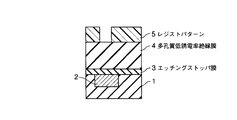
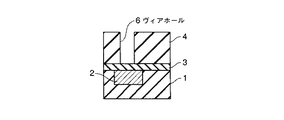
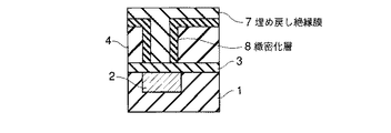
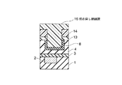
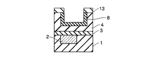
図1乃至図7に、本実施形態にかかる半導体装置の製造方法を表わす断面図を示す。
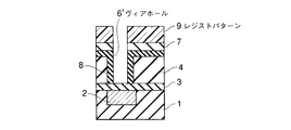
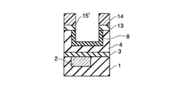
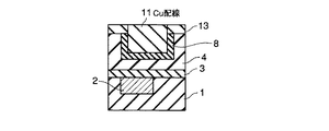
図8乃至図14に、本実施形態にかかる半導体装置の製造方法を表わす断面図を示す。
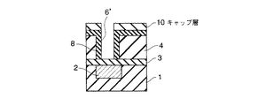
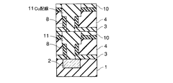
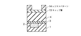
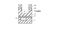
4…多孔質低誘電率絶縁膜; 5…レジストパターン; 6,6’…ヴィアホール
7…埋め戻し絶縁膜; 8…緻密化層; 9,14…レジストパターン
10,13…キャップ層; 11…上層配線; 15,15’…配線溝
16…埋め戻し絶縁膜。
Claims (5)
- 半導体基板上に、多孔質構造を有する低誘電率絶縁膜を形成する工程と、
前記低誘電率絶縁膜に凹部を形成する工程と、
前記凹部が形成された前記低誘電率絶縁膜の上および前記凹部内に、埋め戻し絶縁膜を配置する工程と、
前記凹部内に配置された前記埋め戻し絶縁膜を除去して、前記凹部を再び開口する工程と、
前記凹部に導電性材料を埋め込んで導電部を形成する工程と
を具備することを特徴とする半導体装置の製造方法。 - 前記凹部の再開口は、前記低誘電率絶縁膜上に配置された前記埋め戻し絶縁膜を残して行なうことを特徴とする請求項1に記載の半導体装置の製造方法。
- 前記埋め戻し絶縁膜は、塗布法により形成されることを特徴とする請求項1または2に記載の半導体装置の製造方法。
- 前記埋め戻し絶縁膜は、CVD法により形成されることを特徴とする請求項1または2に記載の半導体装置の製造方法。
- 前記埋め戻し絶縁膜は、有機膜またはSiCOH膜であることを特徴とする請求項1乃至4のいずれか1項に記載の半導体装置の製造方法。
Priority Applications (4)
| Application Number | Priority Date | Filing Date | Title |
|---|---|---|---|
| JP2004107340A JP2005294525A (ja) | 2004-03-31 | 2004-03-31 | 半導体装置の製造方法 |
| TW094106676A TWI260684B (en) | 2004-03-31 | 2005-03-04 | Method of manufacturing semiconductor device |
| US11/072,294 US7329601B2 (en) | 2004-03-31 | 2005-03-07 | Method of manufacturing semiconductor device |
| CNB2005100564876A CN1311540C (zh) | 2004-03-31 | 2005-03-22 | 半导体器件的制造方法 |
Applications Claiming Priority (1)
| Application Number | Priority Date | Filing Date | Title |
|---|---|---|---|
| JP2004107340A JP2005294525A (ja) | 2004-03-31 | 2004-03-31 | 半導体装置の製造方法 |
Publications (1)
| Publication Number | Publication Date |
|---|---|
| JP2005294525A true JP2005294525A (ja) | 2005-10-20 |
Family
ID=35050053
Family Applications (1)
| Application Number | Title | Priority Date | Filing Date |
|---|---|---|---|
| JP2004107340A Pending JP2005294525A (ja) | 2004-03-31 | 2004-03-31 | 半導体装置の製造方法 |
Country Status (4)
| Country | Link |
|---|---|
| US (1) | US7329601B2 (ja) |
| JP (1) | JP2005294525A (ja) |
| CN (1) | CN1311540C (ja) |
| TW (1) | TWI260684B (ja) |
Families Citing this family (25)
| Publication number | Priority date | Publication date | Assignee | Title |
|---|---|---|---|---|
| CA2413592A1 (en) * | 2000-06-23 | 2002-01-03 | Nigel P. Hacker | Method to restore hydrophobicity in dielectric films and materials |
| JP4999454B2 (ja) * | 2003-01-25 | 2012-08-15 | ハネウェル・インターナショナル・インコーポレーテッド | 損傷誘電体材料及び膜の修復及び回復 |
| US7709371B2 (en) * | 2003-01-25 | 2010-05-04 | Honeywell International Inc. | Repairing damage to low-k dielectric materials using silylating agents |
| US8475666B2 (en) * | 2004-09-15 | 2013-07-02 | Honeywell International Inc. | Method for making toughening agent materials |
| US7678712B2 (en) * | 2005-03-22 | 2010-03-16 | Honeywell International, Inc. | Vapor phase treatment of dielectric materials |
| JP2007027436A (ja) * | 2005-07-15 | 2007-02-01 | Toshiba Corp | 半導体装置およびその製造方法 |
| US7556970B2 (en) * | 2006-03-27 | 2009-07-07 | Tokyo Electron Limited | Method of repairing damaged film having low dielectric constant, semiconductor device fabricating system and storage medium |
| JP5120913B2 (ja) * | 2006-08-28 | 2013-01-16 | 国立大学法人東北大学 | 半導体装置および多層配線基板 |
| KR100818106B1 (ko) * | 2006-12-27 | 2008-03-31 | 주식회사 하이닉스반도체 | 기공 형성용 템플레이트 유도체 및 이를 이용한 절연막의 제조방법 |
| US8202807B2 (en) * | 2006-12-27 | 2012-06-19 | Hynix Semiconductor Inc. | Template derivative for forming ultra-low dielectric layer and method of forming ultra-low dielectric layer using the same |
| GB2457956B (en) * | 2008-02-29 | 2012-03-28 | Radiodetection Ltd | System for and method of detecting a buried conductor |
| US9991311B2 (en) | 2008-12-02 | 2018-06-05 | Arizona Board Of Regents On Behalf Of Arizona State University | Dual active layer semiconductor device and method of manufacturing the same |
| US9721825B2 (en) | 2008-12-02 | 2017-08-01 | Arizona Board Of Regents, A Body Corporate Of The State Of Arizona, Acting For And On Behalf Of Arizona State University | Method of providing a flexible semiconductor device and flexible semiconductor device thereof |
| WO2010065459A2 (en) * | 2008-12-02 | 2010-06-10 | Arizona Board Of Regents, For And On Behalf Of Arizona State University | Method of etching organosiloxane dielectric material and semiconductor device thereof |
| US9601530B2 (en) | 2008-12-02 | 2017-03-21 | Arizona Board Of Regents, A Body Corporated Of The State Of Arizona, Acting For And On Behalf Of Arizona State University | Dual active layer semiconductor device and method of manufacturing the same |
| WO2010065457A2 (en) * | 2008-12-02 | 2010-06-10 | Arizona Board Of Regents, For And On Behalf Of Arizona State University | Method of providing a semiconductor device with a dielectric layer and semiconductor device thereof |
| KR101362025B1 (ko) | 2009-05-29 | 2014-02-13 | 아리조나 보드 오브 리젠츠 퍼 앤 온 비하프 오브 아리조나 스테이트 유니버시티 | 고온에서 가요성 반도체 장치를 제공하는 방법 및 그 가요성 반도체 장치 |
| WO2012021196A2 (en) | 2010-05-21 | 2012-02-16 | Arizona Board Of Regents, For And On Behalf Of Arizona State University | Method for manufacturing electronic devices and electronic devices thereof |
| WO2012021197A2 (en) | 2010-05-21 | 2012-02-16 | Arizona Board Of Regents, For And On Behalf Of Arizona State University | Method of manufacturing electronic devices on both sides of a carrier substrate and electronic devices thereof |
| WO2015156891A2 (en) | 2014-01-23 | 2015-10-15 | Arizona Board Of Regents, Acting For And On Behalf Of Arizona State University | Method of providing a flexible semiconductor device and flexible semiconductor device thereof |
| WO2017034644A2 (en) | 2015-06-09 | 2017-03-02 | ARIZONA BOARD OF REGENTS a body corporate for THE STATE OF ARIZONA for and on behalf of ARIZONA STATE UNIVERSITY | Method of providing an electronic device and electronic device thereof |
| US10381224B2 (en) | 2014-01-23 | 2019-08-13 | Arizona Board Of Regents On Behalf Of Arizona State University | Method of providing an electronic device and electronic device thereof |
| KR102466741B1 (ko) | 2014-05-13 | 2022-11-15 | 아리조나 보드 오브 리젠츠 온 비하프 오브 아리조나 스테이트 유니버시티 | 전자 디바이스를 제공하는 방법 |
| US10446582B2 (en) | 2014-12-22 | 2019-10-15 | Arizona Board Of Regents On Behalf Of Arizona State University | Method of providing an imaging system and imaging system thereof |
| US9741742B2 (en) | 2014-12-22 | 2017-08-22 | Arizona Board Of Regents, A Body Corporate Of The State Of Arizona, Acting For And On Behalf Of Arizona State University | Deformable electronic device and methods of providing and using deformable electronic device |
Family Cites Families (11)
| Publication number | Priority date | Publication date | Assignee | Title |
|---|---|---|---|---|
| US6380096B2 (en) * | 1998-07-09 | 2002-04-30 | Applied Materials, Inc. | In-situ integrated oxide etch process particularly useful for copper dual damascene |
| JP3585384B2 (ja) * | 1998-12-22 | 2004-11-04 | 松下電器産業株式会社 | 半導体装置の製造方法 |
| JP3084367B1 (ja) | 1999-03-17 | 2000-09-04 | キヤノン販売株式会社 | 層間絶縁膜の形成方法及び半導体装置 |
| JP2001345380A (ja) | 2000-05-31 | 2001-12-14 | Toshiba Corp | 半導体装置の製造方法および半導体装置 |
| US7164206B2 (en) * | 2001-03-28 | 2007-01-16 | Intel Corporation | Structure in a microelectronic device including a bi-layer for a diffusion barrier and an etch-stop layer |
| JP2002353308A (ja) | 2001-05-28 | 2002-12-06 | Toshiba Corp | 半導体装置及びその製造方法 |
| JP3886779B2 (ja) * | 2001-11-02 | 2007-02-28 | 富士通株式会社 | 絶縁膜形成用材料及び絶縁膜の形成方法 |
| US6790770B2 (en) * | 2001-11-08 | 2004-09-14 | Taiwan Semiconductor Manufacturing Co., Ltd | Method for preventing photoresist poisoning |
| KR100448592B1 (ko) * | 2001-12-29 | 2004-09-13 | 주식회사 하이닉스반도체 | 반도체 소자의 구리배선 형성 방법 |
| JP2003282698A (ja) | 2002-03-22 | 2003-10-03 | Sony Corp | 半導体装置の製造方法および半導体装置 |
| JP3967196B2 (ja) | 2002-05-30 | 2007-08-29 | 富士通株式会社 | 半導体装置及びその製造方法 |
-
2004
- 2004-03-31 JP JP2004107340A patent/JP2005294525A/ja active Pending
-
2005
- 2005-03-04 TW TW094106676A patent/TWI260684B/zh not_active IP Right Cessation
- 2005-03-07 US US11/072,294 patent/US7329601B2/en not_active Expired - Fee Related
- 2005-03-22 CN CNB2005100564876A patent/CN1311540C/zh not_active Expired - Fee Related
Also Published As
| Publication number | Publication date |
|---|---|
| CN1677642A (zh) | 2005-10-05 |
| US20050233583A1 (en) | 2005-10-20 |
| US7329601B2 (en) | 2008-02-12 |
| CN1311540C (zh) | 2007-04-18 |
| TW200535952A (en) | 2005-11-01 |
| TWI260684B (en) | 2006-08-21 |
Similar Documents
| Publication | Publication Date | Title |
|---|---|---|
| JP2005294525A (ja) | 半導体装置の製造方法 | |
| CN100483698C (zh) | 多孔低k介质互连结构 | |
| JP3276963B2 (ja) | 誘電体フィルムを基盤上に形成する方法 | |
| CN101593689B (zh) | 光刻图案的形成方法和双镶嵌结构的制造方法 | |
| US8202803B2 (en) | Method to remove capping layer of insulation dielectric in interconnect structures | |
| JP5180426B2 (ja) | 半導体装置の製造方法 | |
| CN101090067B (zh) | 半导体装置的制造方法 | |
| US8334203B2 (en) | Interconnect structure and method of fabricating | |
| US8415248B2 (en) | Self-aligned dual damascene BEOL structures with patternable low-k material and methods of forming same | |
| US20050245100A1 (en) | Reliability improvement of SiOC etch with trimethylsilane gas passivation in Cu damascene interconnects | |
| JP2001077196A (ja) | 半導体装置の製造方法 | |
| JP2001044191A (ja) | 積層絶縁膜とその製造方法および半導体装置とその製造方法 | |
| JP2006128543A (ja) | 電子デバイスの製造方法 | |
| WO2004090974A1 (ja) | 電子デバイス及びその製造方法 | |
| JP2000294634A (ja) | 半導体装置及びその製造方法 | |
| CN100552542C (zh) | 由旋涂上的陶瓷薄膜组成的构图层 | |
| JP2007281114A (ja) | 半導体装置の製造方法および半導体装置 | |
| US20040183164A1 (en) | Semiconductor device with improved reliability and manufacturing method of the same | |
| CN101231968A (zh) | 镶嵌内连线结构与双镶嵌工艺 | |
| US7728065B2 (en) | Material for forming exposure light-blocking film, multilayer interconnection structure and manufacturing method thereof, and semiconductor device | |
| JP2000243749A (ja) | 絶縁膜の形成方法 | |
| JPH11233630A (ja) | 半導体装置の製造方法およびこれを用いた半導体装置 | |
| JP4223012B2 (ja) | 絶縁膜の形成方法、多層構造の形成方法および半導体装置の製造方法 | |
| JP4311947B2 (ja) | 半導体装置 | |
| JP2005093688A (ja) | 半導体装置および半導体装置の製造方法 |
Legal Events
| Date | Code | Title | Description |
|---|---|---|---|
| A977 | Report on retrieval |
Free format text: JAPANESE INTERMEDIATE CODE: A971007 Effective date: 20061010 |
|
| A131 | Notification of reasons for refusal |
Free format text: JAPANESE INTERMEDIATE CODE: A131 Effective date: 20061017 |
|
| A521 | Request for written amendment filed |
Free format text: JAPANESE INTERMEDIATE CODE: A523 Effective date: 20061218 |
|
| A131 | Notification of reasons for refusal |
Free format text: JAPANESE INTERMEDIATE CODE: A131 Effective date: 20070703 |
|
| A02 | Decision of refusal |
Free format text: JAPANESE INTERMEDIATE CODE: A02 Effective date: 20071030 |