US6984875B2 - Semiconductor device with improved reliability and manufacturing method of the same - Google Patents
Semiconductor device with improved reliability and manufacturing method of the same Download PDFInfo
- Publication number
- US6984875B2 US6984875B2 US10/765,094 US76509404A US6984875B2 US 6984875 B2 US6984875 B2 US 6984875B2 US 76509404 A US76509404 A US 76509404A US 6984875 B2 US6984875 B2 US 6984875B2
- Authority
- US
- United States
- Prior art keywords
- layer
- film
- semiconductor device
- trench
- modified
- Prior art date
- Legal status (The legal status is an assumption and is not a legal conclusion. Google has not performed a legal analysis and makes no representation as to the accuracy of the status listed.)
- Expired - Lifetime
Links
Images


Classifications
-
- H—ELECTRICITY
- H10—SEMICONDUCTOR DEVICES; ELECTRIC SOLID-STATE DEVICES NOT OTHERWISE PROVIDED FOR
- H10W—GENERIC PACKAGES, INTERCONNECTIONS, CONNECTORS OR OTHER CONSTRUCTIONAL DETAILS OF DEVICES COVERED BY CLASS H10
- H10W20/00—Interconnections in chips, wafers or substrates
- H10W20/01—Manufacture or treatment
- H10W20/071—Manufacture or treatment of dielectric parts thereof
- H10W20/074—Manufacture or treatment of dielectric parts thereof of dielectric parts comprising thin functional dielectric layers, e.g. dielectric etch-stop, barrier, capping or liner layers
- H10W20/076—Manufacture or treatment of dielectric parts thereof of dielectric parts comprising thin functional dielectric layers, e.g. dielectric etch-stop, barrier, capping or liner layers in via holes or trenches
-
- H—ELECTRICITY
- H10—SEMICONDUCTOR DEVICES; ELECTRIC SOLID-STATE DEVICES NOT OTHERWISE PROVIDED FOR
- H10W—GENERIC PACKAGES, INTERCONNECTIONS, CONNECTORS OR OTHER CONSTRUCTIONAL DETAILS OF DEVICES COVERED BY CLASS H10
- H10W20/00—Interconnections in chips, wafers or substrates
- H10W20/01—Manufacture or treatment
- H10W20/071—Manufacture or treatment of dielectric parts thereof
- H10W20/081—Manufacture or treatment of dielectric parts thereof by forming openings in the dielectric parts
-
- H—ELECTRICITY
- H10—SEMICONDUCTOR DEVICES; ELECTRIC SOLID-STATE DEVICES NOT OTHERWISE PROVIDED FOR
- H10W—GENERIC PACKAGES, INTERCONNECTIONS, CONNECTORS OR OTHER CONSTRUCTIONAL DETAILS OF DEVICES COVERED BY CLASS H10
- H10W20/00—Interconnections in chips, wafers or substrates
- H10W20/01—Manufacture or treatment
- H10W20/071—Manufacture or treatment of dielectric parts thereof
- H10W20/093—Manufacture or treatment of dielectric parts thereof by modifying materials of the dielectric parts
- H10W20/096—Manufacture or treatment of dielectric parts thereof by modifying materials of the dielectric parts by contacting with gases, liquids or plasmas
Definitions
- the present invention relates to a semiconductor device and a manufacturing method of the same. More particularly, the present invention relates to a semiconductor device of which reliability is improved and a manufacturing method of the same.
- a signal processing speed of the LSI mainly depend on operating speeds of its transistors and delay time of signal transmission in interconnections (wiring).
- the working speed of the transistor has been increasing by reducing its size.
- the influence of the delay of signal transmission in the interconnections has been increasing on the signal processing speed in the LSI, especially in the LSI having multilayer interconnections.
- copper (Cu) has been substituting for aluminum (Al) as a material used for the interconnection.
- low dielectric constant film has been substituting for silicon dioxide as a material used for an interlayer insulating film (an interlayer dielectric).
- the low dielectric constant film is mainly categorized by two kinds of material groups.
- One group includes Si—O basis materials.
- Another group includes organic resin basis materials.
- As for the Si—O basis materials a methylpolysiloxane film with the Si—O with methyl radicals as organic radicals and a methyl silsesquioxane (hereinafter referred to as a MSQ) film are known as insulating films.
- the film made from the organic resin basis materials is inferior to that made from the Si—O basis materials in its mechanical strength and dielectric characteristics. Therefore, it is difficult to integrate multilayer interconnections and obtain a high reliability by using the organic resin basis materials rather than using the Si—O basis materials. Hence, it is difficult to realize an advanced device with multilayer interconnections by using the organic resin basis materials.
- FIG. 1 is a cross sectional view showing a conventional semiconductor device.
- a first SiCN film 202 is formed as a barrier insulating film on an insulating film 201 formed on a semiconductor substrate that includes transistors.
- a MSQ film 213 which is one of an organo-polysiloxane film, is formed on the first SiCN film 202 .
- a SiO 2 film 204 is formed on the MSQ film 213 .
- the trenches for the interconnections are formed through the first SiCN film 202 , MSQ film 213 and the SiO 2 film 204 .
- a MSQ modified film 215 is formed in the side wall of the trench.
- the MSQ modified film 215 is formed by exposing the MSQ film 213 in oxygen plasma when the ashing processing is carried out to the trenches (described in Japanese Laid Open Patent Application (JP-A 2002-246383)).
- the MSQ modified film 215 is characterized by that the film thickness of the upper part is substantially the same as that of the lower part.
- a TaN film 206 is formed as one of barrier metals on the inner surface of the trench.
- a Ta film 207 is formed as another barrier metal on the TaN film 206 .
- a Cu film 208 is formed on the Ta film 207 such that the Cu film 208 fill up the trench.
- the interconnection is composed of the TaN film 206 , the Ta film 207 and the Cu film 208 .
- a second SiCN film 209 is formed as a barrier insulating film on the SiO 2 film 204 and the interconnections.
- the trench only for interconnection is illustrated. However, repetition to form a via on the trench and another interconnection on the via enables to form the multilayer interconnections.
- the trench has taper shape, the width of the upper part tends to be wider than that of the lower part. Therefore, the interval between the adjacent interconnections of the upper part is closer than that of the lower part. This causes that the electric field is concentrated at the upper part of the interconnections, which may bring about dielectric breakdown.
- the MSQ modified film includes smaller amount of carbon element than the MSQ film and its composition is close to SiO 2 .
- the etching rate by buffered hydrogen fluoride of the MSQ modified film solution is faster than that of the MSQ film. Therefore, it is easy to confirm the MSQ modified film and the MSQ film by observing the SEM cross sectional view of the semiconductor device after the etching.
- FIGS. 2A to 2C and FIGS. 3A and 3B are the cross sectional views showing the procedure of the conventional manufacturing method of the semiconductor device.
- the first SiCN film 202 is formed by using the plasma CVD method on the insulating film 201 formed on the semiconductor substrate.
- the thickness of the first SiCN film 202 is 50 nm to 100 nm.
- the material of the MSQ film 213 is coated and baked on the first SiCN film 202 such that the MSQ film 213 is formed with the film thickness of 150 nm to 350 nm.
- the SiO 2 film 204 with the thickness of 50 nm to 200 nm is formed by using the plasma CVD method on the MSQ film 213 .
- an ARC (anti-reflection coating) film 212 is coated on the SiO 2 film 204 .
- the photoresist mask 216 patterned by using the photolithography technique with the lower limit of 0.14-micrometer level.
- the dry etching processing is carried out to ARC film 212 , the SiO 2 film 204 and the MSQ film 213 through the photoresist mask 216 by using gas including CHF 3 .
- the dry etching is stopped at the surface of the first SiCN film 202 .
- the photoresist mask 216 is removed by oxygen plasma ashing. After that, residual is completely removed by using the organic remover with amine related material.
- the first SiCN film 202 is etched back to be removed. As a result, the trench 220 is formed in the SiO 2 film 204 , the MSQ film 213 and the first SiCN film 202 .
- the MSQ modified film 215 is formed on the side wall of the trench 220 .
- the MSQ modified film 215 is characterized by that the film thickness of the upper part is substantially the same as that of the lower part.
- the film thickness of the upper part and the lower part is approximately less than 10 nm.
- the TaN film 206 with the thickness of 10 nm is formed as one of barrier metals on the inner surface of the trench 220 .
- the Ta film 207 with the thickness of 20 nm is formed as another barrier metal on the TaN film 206 .
- the Cu seed film (not shown) with the thickness of 100 nm is formed on the Ta film 207 .
- the Cu film 208 with the thickness of 600 nm is formed on the Cu seed film by using Cu metal plating. Then, the semiconductor device is annealed in a furnace in the temperature range of 200 to 400 degrees Celsius.
- the metals (the TaN film 206 , the Ta film 207 and the Cu film 208 ) are removed except for those in the trench 220 by using CMP (chemical mechanical polishing) technique.
- CMP chemical mechanical polishing
- the MSQ film has mechanical strength lower than SiO 2 by one order of magnitude. Therefore, heavy load generated by the CMP processing and the wire bonding processing brings about the film peeling of the MSQ film 213 .
- the MSQ film has low dielectric breakdown voltage. Particularly, the interval between the upper parts of adjacent interconnections is shorter than that between the lower parts. This makes interlayer insulating film corresponding to the upper parts of the interconnections weak in its dielectric breakdown strength in case of using the MSQ film.
- the SiO 2 as a hard mask on the low dielectric constant film is etched by the erosion in the CMP processing, the SiCN film as a cap film is formed almost directly on the low dielectric constant film. This causes that the concentration of electric field becomes remarkably high near the boundary of the SiCN film and the low dielectric constant film. Therefore, the dielectric breakdown voltage of the interconnections is reduced and the dielectric breakdown might occur. It generates the problem of the decrease of the reliability of the semiconductor device.
- Japanese Laid Open Patent Application JP-A 2002-246383 discloses the following a forming method of an insulating film and a manufacturing method of a semiconductor device.
- the forming method of an insulating film includes: preparing a solution by dissolving a first polymer and a second polymer to a solvent, each of the polymers includes mainly methylpolysiloxane and an average molecular weight of one of the polymers has more than ten times larger than that of another; and forming a coating film by coating the solution on a semiconductor substrate; and an organic silicon oxide film by thermally polymerizing the first polymer and the second polymer.
- Japanese Laid Open Patent Application JP-A 2003-17561 discloses the following a manufacturing method of a semiconductor device and a semiconductor device.
- This manufacturing method of a semiconductor device includes: forming a first isolating film made from low dielectric constant material with carbon on a semiconductor substrate; forming a low carbon concentration layer in a surface of the first insulating film by processing the surface to reduce the carbon concentration of the surface; forming a second insulating film on the low carbon concentration layer; forming a trench in the first and second insulating film for metal to be embedded; embedding the metal in the trench in the insulating films; and forming a interconnection by polishing a surface of the embedded metal.
- Japanese Laid Open Patent Application JP-A 2001-326222 discloses the following a semiconductor device, a semiconductor wafer and a manufacturing method of the same.
- This semiconductor device includes a multilayer insulating film having interconnections on a semiconductor substrate.
- the multilayer insulating film includes a first insulating film made from an organic lower dielectric constant material than silicon dioxide, a second insulating film made from a polysiloxane compound with Si—H group formed on the first insulating film, a third insulating film made from an inorganic material formed on the second insulating film.
- Japanese Laid Open Patent Application JP-A 2000-294634 discloses the following a semiconductor device and a manufacturing method of the same.
- This semiconductor device includes a plurality of interconnections on a substrate, wherein metals are placed between the interconnections.
- An inorganic insulating film is arranged at the side wall faced to adjacent interconnection.
- Japanese Laid Open Patent Application JP-A Heisei 11(1999)-87502 discloses the following a manufacturing method of a semiconductor device.
- This manufacturing method of a semiconductor device includes: forming a first insulating film on a substrate having a first interconnection layer; forming a second insulating film on the first insulating film and a third insulating film on the second insulating film, sequentially; forming a first resist pattern having an opening pattern corresponding to the a connection hole for the first interconnection on the third insulating film; transferring the pattern of the first resist pattern to the third insulating film by selectively etching the third insulating film while using the first resist pattern as a mask and the second insulating film as an anti-etching mask for the first insulating film; and removing the first resist pattern by using the second insulating film as a protect mask for the first insulating film.
- an object of the present invention is to provide a semiconductor device of which reliability is improved and a manufacturing method of the same.
- Another object of the present invention is to provide a semiconductor device of which dielectric breakdown strength is improved and a manufacturing method of the same.
- Still another object of the present invention is to provide a semiconductor device of which mechanical strength is improved and a manufacturing method of the same.
- the present invention provides a semiconductor device including an insulating layer, a conducting portion and a modified layer.
- the insulating layer is formed on a semiconductor substrate.
- the conducting portion is formed in the insulating layer.
- the modified layer is formed between the insulating layer and the conducting portion.
- the insulating layer includes hydrogenated polysiloxane.
- the modified layer is a layer to which the hydrogenated polysiloxane is modified.
- a portion of the modified layer far from the semiconductor substrate is thicker than a portion of the modified layer near the semiconductor substrate.
- a portion of the conducting portion far from the semiconductor substrate is thicker than a portion of the conducting portion near the semiconductor substrate.
- the modified layer is a layer to which the hydrogenated polysiloxane is oxidized.
- the hydrogenated polysiloxane includes at least one of a ladder type hydrogenated polysiloxane and a porous ladder type hydrogenated polysiloxane.
- the conducting portion is a wiring
- the modified layer is formed to attach to a side of the wiring.
- a portion of the conducting portion far from the semiconductor substrate is thicker than a portion of the conducting portion near the semiconductor substrate.
- the conducting portion includes a first conducting portion and a second conducting portion.
- the first conducting portion is a bottom and side part of the conducting portion.
- the second conducting portion is a remaining part of the conducting portion, made form copper.
- the present invention provides a manufacturing method of a semiconductor device, including: (a) forming an insulating film on a semiconductor substrate, wherein the insulating film includes hydrogenated polysiloxane; (b) etching the insulating film to form a trench, wherein an etching gas including a fluorocarbon gas and an oxidant gas is used for the etching; and (c) forming an interconnection in the trench.
- the step (b) includes (b 1 ) transforming a part of the insulating film to a modified layer by using the etching gas, wherein the part of the insulating film is in a side wall of the trench.
- a portion of the modified layer far from the semiconductor substrate is thicker than a portion of the modified layer near the semiconductor substrate.
- the oxidant gas includes at least one of O 2 , CO and CO 2 .
- the fluorocarbon gas includes at least one of CF 4 , C 4 F 8 , C 5 F 8 , C 2 F 6 , CH 2 F 2 and CHF 3 .
- a portion of the modified layer far from the semiconductor substrate is thicker than a portion of the modified layer near the semiconductor substrate.
- a semiconductor device including: a first insulating layer formed on a substrate; a trench formed in the first insulating layer; a conductive layer formed in the trench; and a second insulating layer formed between the first insulating layer and the conductive layer.
- the trench has a part which is wider than the other part. A thickness of the second insulating layer adjacent to the wider part is thicker than the other part.
- the trench has a width which is wider at upper part than lower part, and a thickness of the second insulating layer adjacent to the upper part is thicker than a thickness of the second insulating layer adjacent to the lower part.
- the semiconductor device includes the modified hydrogenated polysiloxane film as a part of the interlayer insulating film, of which the upper part is thicker than the lower part.
- the mechanical strength of the modified hydrogenated polysiloxane film is higher than that of the original hydrogenated polysiloxane film, the mechanical strength is improved.
- the dielectric constant of the modified hydrogenated polysiloxane film is larger than that of the original hydrogenated polysiloxane film, the dielectric breakdown strength is improved.
- FIG. 1 is a cross sectional view showing a conventional semiconductor device
- FIGS. 2A to 2C and FIGS. 3A and 3B are the cross sectional views showing a procedure of the conventional manufacturing method of the semiconductor device
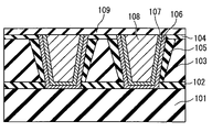
- FIG. 4 is a cross sectional view showing an embodiment of a semiconductor device according to the present invention.
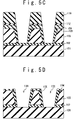
- FIGS. 5A to 5D and FIGS. 6A and 6B are the cross sectional views showing an embodiment of a procedure of the manufacturing method of the semiconductor device according to the present invention.
- FIG. 7 is a graph showing dielectric breakdown strength of the interlayer insulating film of the same layer.
- FIG. 8 is a graph showing the failure of the bonding processing for the semiconductor device with the five-layer interconnection.
- FIG. 4 is a cross sectional view showing an embodiment of a semiconductor device according to the present invention.
- an insulating film made from ladder type hydrogenated polysiloxane (L-Ox: Ladder-Oxide, a trade mark), one of hydrogenated polysiloxanes, is shown as an example for a low dielectric constant interlayer insulating film.
- a first SiCN film 102 is formed as a barrier insulating film on an insulating film 101 formed on a semiconductor substrate that includes transistors.
- An interlayer insulating film 103 which is the ladder type hydrogenated polysiloxane film, is formed on the first SiCN film 102 .
- a SiO 2 film 104 is formed on the interlayer insulating film 103 .
- the trenches for the interconnections are formed through the first SiCN film 102 , the interlayer insulating film 103 and the SiO 2 film 104 .
- a modified insulating film 105 is formed in the side wall of the trench in the interlayer insulating film 103 .
- the modified insulating film 105 is formed on the surface of the trench.
- the modified insulating film 105 is characterized by that the film thickness of the upper part is thicker than that of the lower part.
- a TaN film 106 is formed as one of barrier metals on the inner surface of the trench, close against the modified insulating film 105 .
- a Ta film 107 is formed as another barrier metal on the TaN film 106 .
- a Cu film 108 is formed on the Ta film 107 such that the Cu film 108 fill up the trench.
- the interconnection is composed of the TaN film 106 , the Ta film 107 and the Cu film 108 .
- a second SiCN film 109 is formed as a barrier insulating film on the SiO 2 film 104 and the interconnections.
- the trench for interconnection is illustrated. However, repetition to form a via on the trench and another interconnection on the via enables to form the multilayer interconnections.
- the trench has taper shape, the width of the upper part tends to be wider than that of the lower part. Therefore, if the modified insulating film 105 is not provided, the interval between the interconnections of the upper part is closer than that of the lower part. This causes that the electric field tends to be concentrated on the upper part of the trench.
- the upper part of the modified insulating film 105 is thicker than the lower part.
- the modified insulating film 105 includes smaller amount of carbon element than the interlayer insulating film 103 made from the hydrogenated polysiloxane and its composition is close to SiO 2 . Therefore, the modified insulating film 105 is superior to the interlayer insulating film 103 in its dielectric characteristics. Hence, the dielectric characteristics will be improved.
- the etching rate by buffered hydrogen fluoride of the modified insulating film 105 solution is faster than that of the interlayer insulating film 103 . It is easy to confirm the modified insulating film 105 and the interlayer insulating film 103 by observing the SEM cross sectional view of the semiconductor device after the etching.
- FIGS. 5A to 5D and FIGS. 6A and 6B are the cross sectional views showing an embodiment of a procedure of the manufacturing method of the semiconductor device according to the present invention.
- the first SiCN film 102 is formed by using the plasma CVD method on the insulating film 101 formed on a semiconductor substrate having semiconductor elements such as transistors.
- the thickness of the first SiCN film 102 is 50 nm to 100 nm.
- the material of the interlayer insulating film 103 is coated and baked on the first SiCN film 102 such that the interlayer insulating film 103 is formed with the film thickness of 150 nm to 350 nm.
- the SiO 2 film 104 with the thickness of 50 nm to 200 nm is formed by using the plasma CVD method on the interlayer insulating film 103 .
- an ARC (anti-reflection coating) film 112 is coated on the SiO 2 film 104 .
- the dry etching processing is carried out to ARC film 112 , the SiO 2 film 104 and the interlayer insulating film 103 through the photoresist mask 116 by using gas including C 4 F 8 gas and O 2 gas.
- the dry etching is stopped at the surface of the first SiCN film 102 .
- the photoresist mask 116 is removed by using oxygen plasma ashing processing. After that, residual is completely removed by using the weak alkaline organic remover with amine related material.
- the first SiCN film 102 is etched back to be removed.
- the trench 120 is formed in the SiO 2 film 104 , the interlayer insulating film 103 and the first SiCN film 102 .
- the modified insulating film 105 is formed on the side wall of the trench 120 .
- the modified insulating film 105 is formed such that the film thickness of the upper part is thicker than that of the lower part.
- the film thickness of the most upper part is approximately 30 nm, and the most lower part is approximately 10 nm.
- the TaN film 106 with the thickness of 10 nm is formed as one of barrier metals on the inner surface of the trench 120 .
- the Ta film 107 with the thickness of 20 nm is formed as another barrier metal on the TaN film 106 .
- the Cu seed film (not shown) with the thickness of 100 nm is formed on the Ta film 107 .
- the Cu film 108 with the thickness of 600 nm is formed on the Cu seed film by using Cu metal plating.
- the semiconductor device is annealed in the furnace in the temperature range of 200 to 400 degree Celsius.
- the metals (the TaN film 106 , the Ta film 107 and the Cu film 108 ) are removed except for those in the trench 120 by using CMP (chemical mechanical polishing) technique.
- CMP chemical mechanical polishing
- the second SiCN film 109 with the thickness of 50 to 100 nm is formed by using the plasma CVD method on the SiO 2 film 104 and the interconnections.
- the shape of the modified insulating film 105 is realized by etching the interlayer insulating film 103 by using an etching gas including at least fluorocarbon gas and oxidant gas. including C 4 F 8 gas and O 2 gas. Addition of the oxidant gas to the etching gas, the interlayer insulating film 103 is oxidized to be the modified insulating film 105 during the dry etching.
- the upper part becomes thicker because the upper part is exposed to oxygen (ex. oxygen ion, oxygen radical) more directly for a longer time.
- C 4 F 8 gas is used as the fluorocarbon gas.
- the gas including at least one of CF 4 , C 4 F 8 , C 5 F 8 , C 2 F 6 , CH 2 F 2 and CHF 3 may be used as the fluorocarbon gas and the above-mentioned same result can be obtained.
- O 2 gas is used as the oxidant gas.
- the gas including at least one of O 2 , CO and CO 2 may be used as the oxidant gas and the above-mentioned same result can be obtained.
- FIG. 7 is a graph showing dielectric breakdown of the interlayer insulating film between the interconnections of the same layer.
- the vertical axis shows the breakdown time (a. u.)
- MSQ shows the MSQ film as the interlayer insulating film according to the conventional technique
- L-Ox shows the ladder type hydrogenated polysiloxane film as the interlayer insulating film according to the present invention.
- the breakdown time is measured under the interconnections' interval of 0.14 micrometer, the electric field of 2 MV/cm and the temperature of 125 degree Celsius.
- the breakdown time of the present invention was improved to 22 (twenty two).
- the upper part of the modified insulating film 105 is thicker than the lower part.
- the interconnection has taper shape, the width of the upper part tends to be wider than that of the lower part. Therefore, the interval between the interconnections of the upper part is closer than that of the lower part. This causes that the electric field tends to be concentrated on the upper part of the interconnection.
- the dielectric constant of the modified insulating film 105 is higher than that of interlayer insulating film 103 of the hydrogenated polysiloxane film and closer to that of SiO2.
- the modified insulating film 105 can release the concentration of the electric field.
- the fact that the upper part of the modified insulating film 105 is thicker than the lower part is also important point to release the concentration.
- FIG. 8 is a graph showing the failure of the bonding processing for the semiconductor device with the five-layer interconnection.
- the vertical axis shows the failure (%)
- MSQ shows the MSQ film as the interlayer insulating film according to the conventional technique
- L-Ox shows the ladder type hydrogenated polysiloxane film as the interlayer insulating film according to the present invention.
- the defectives were generated in the rate of 2% in case of using the MSQ film.
- the defectives were not generated in case of using the hydrogenated polysiloxane film.
- the defects were generated at the boundary between the upper part of interconnection and the SiCN film. It is suggested that the mechanical load is concentrated to the upper part of the interconnection.
- the mechanical strength of the MSQ film is similar to that of the hydrogenated polysiloxane film. Therefore, it is supposed that the difference of the defect generation between the conventional technique and the present invention is caused by the difference between the MSQ modified film ( 215 ) and the modified insulating film ( 105 ).
- the semiconductor device of the present invention has the resistance property to the bonding processing.
- the trench tend to be a bowing shape remarkably that is not desirable. This may be because the carbons of the methyl radicals in the MSQ film is drawn out by the oxidant gas and the MSQ film is constricted rapidly.
- the interlayer insulating film of the ladder type hydrogenated polysiloxane film adding the oxidant gas to the fluorocarbon gas enables the shape of the trench to be stable.
- the interlayer insulating film is not constricted rapidly and the hydorgen in the film is oxidized, by the oxidant gas. Therefore, the part of the interlayer insulating film is modified to the modified insulating film similar to the SiO 2 .
- this modified insulating film is worked as a protect film, the trench shape is stable. If the oxidant gas is not used, the dry etching can not be proceeded because the deposition film may be deposited on the etching surface.
- the present invention is not limited to this embodiment.
- the present invention enables to avoid the film peeling in the processing with the heavy load such as the CMP processing, and the defectives caused by the bonding in the chip assembly processing.
Landscapes
- Internal Circuitry In Semiconductor Integrated Circuit Devices (AREA)
- Drying Of Semiconductors (AREA)
Abstract
Description
Claims (18)
Applications Claiming Priority (2)
| Application Number | Priority Date | Filing Date | Title |
|---|---|---|---|
| JP2003-019411 | 2003-01-28 | ||
| JP2003019411A JP3676784B2 (en) | 2003-01-28 | 2003-01-28 | Semiconductor device and manufacturing method thereof |
Publications (2)
| Publication Number | Publication Date |
|---|---|
| US20040183164A1 US20040183164A1 (en) | 2004-09-23 |
| US6984875B2 true US6984875B2 (en) | 2006-01-10 |
Family
ID=32949272
Family Applications (1)
| Application Number | Title | Priority Date | Filing Date |
|---|---|---|---|
| US10/765,094 Expired - Lifetime US6984875B2 (en) | 2003-01-28 | 2004-01-28 | Semiconductor device with improved reliability and manufacturing method of the same |
Country Status (2)
| Country | Link |
|---|---|
| US (1) | US6984875B2 (en) |
| JP (1) | JP3676784B2 (en) |
Cited By (4)
| Publication number | Priority date | Publication date | Assignee | Title |
|---|---|---|---|---|
| WO2014066740A1 (en) | 2012-10-26 | 2014-05-01 | Element Six Technologies Us Corporation | Semiconductor devices with improved reliability and operating life and methods of manufacturing the same |
| RU2590214C1 (en) * | 2015-04-16 | 2016-07-10 | Акционерное общество "НПО "Орион" | Method of increasing reliability of matrix photoelectronic modules |
| US9861268B2 (en) | 1999-03-01 | 2018-01-09 | West View Research, Llc | Methods of processing data obtained from medical device |
| US9861296B2 (en) | 1999-03-01 | 2018-01-09 | West View Research, Llc | Ingestible probe with agent delivery |
Families Citing this family (7)
| Publication number | Priority date | Publication date | Assignee | Title |
|---|---|---|---|---|
| JP4878434B2 (en) | 2004-09-22 | 2012-02-15 | ルネサスエレクトロニクス株式会社 | Semiconductor device and manufacturing method thereof |
| DE102005006231B4 (en) * | 2005-02-10 | 2007-09-20 | Ovd Kinegram Ag | Method for producing a multilayer body |
| JP4739917B2 (en) * | 2005-11-07 | 2011-08-03 | 富士通セミコンダクター株式会社 | Stripping method of resist mask |
| JP2009147096A (en) * | 2007-12-14 | 2009-07-02 | Panasonic Corp | Semiconductor device and manufacturing method thereof |
| US8018023B2 (en) | 2008-01-14 | 2011-09-13 | Kabushiki Kaisha Toshiba | Trench sidewall protection by a carbon-rich layer in a semiconductor device |
| JP2012038961A (en) * | 2010-08-09 | 2012-02-23 | Renesas Electronics Corp | Semiconductor device and method of manufacturing the same |
| JP7629875B2 (en) * | 2020-01-30 | 2025-02-14 | ソニーセミコンダクタソリューションズ株式会社 | Semiconductor device and etching method |
Citations (8)
| Publication number | Priority date | Publication date | Assignee | Title |
|---|---|---|---|---|
| JPH1187502A (en) | 1997-09-09 | 1999-03-30 | Toshiba Corp | Method for manufacturing semiconductor device |
| JP2000294634A (en) | 1999-04-07 | 2000-10-20 | Nec Corp | Semiconductor device and manufacturing method thereof |
| US20010017422A1 (en) * | 1999-12-21 | 2001-08-30 | Noriaki Oda | Semiconductor device with copper-based wiring lines and method of fabricating the same |
| JP2001326222A (en) | 2000-05-16 | 2001-11-22 | Nec Corp | Semiconductor device, semiconductor wafer, and manufacturing method thereof |
| JP2002110644A (en) | 2000-09-28 | 2002-04-12 | Nec Corp | Etching method |
| JP2002246383A (en) | 2000-12-15 | 2002-08-30 | Toshiba Corp | Method for forming insulating film and method for manufacturing semiconductor device |
| JP2003017561A (en) | 2001-06-29 | 2003-01-17 | Toshiba Corp | Semiconductor device manufacturing method and semiconductor device |
| JP2003533025A (en) | 2000-04-28 | 2003-11-05 | 東京エレクトロン株式会社 | Semiconductor device having low dielectric constant film and method of manufacturing the same |
-
2003
- 2003-01-28 JP JP2003019411A patent/JP3676784B2/en not_active Expired - Fee Related
-
2004
- 2004-01-28 US US10/765,094 patent/US6984875B2/en not_active Expired - Lifetime
Patent Citations (9)
| Publication number | Priority date | Publication date | Assignee | Title |
|---|---|---|---|---|
| JPH1187502A (en) | 1997-09-09 | 1999-03-30 | Toshiba Corp | Method for manufacturing semiconductor device |
| US6051508A (en) * | 1997-09-09 | 2000-04-18 | Kabushiki Kaisha Toshiba | Manufacturing method of semiconductor device |
| JP2000294634A (en) | 1999-04-07 | 2000-10-20 | Nec Corp | Semiconductor device and manufacturing method thereof |
| US20010017422A1 (en) * | 1999-12-21 | 2001-08-30 | Noriaki Oda | Semiconductor device with copper-based wiring lines and method of fabricating the same |
| JP2003533025A (en) | 2000-04-28 | 2003-11-05 | 東京エレクトロン株式会社 | Semiconductor device having low dielectric constant film and method of manufacturing the same |
| JP2001326222A (en) | 2000-05-16 | 2001-11-22 | Nec Corp | Semiconductor device, semiconductor wafer, and manufacturing method thereof |
| JP2002110644A (en) | 2000-09-28 | 2002-04-12 | Nec Corp | Etching method |
| JP2002246383A (en) | 2000-12-15 | 2002-08-30 | Toshiba Corp | Method for forming insulating film and method for manufacturing semiconductor device |
| JP2003017561A (en) | 2001-06-29 | 2003-01-17 | Toshiba Corp | Semiconductor device manufacturing method and semiconductor device |
Non-Patent Citations (1)
| Title |
|---|
| Andrews, "Polysiloxane Modifications", Protective Coatings Worldwide, http://www.international-pc.com/pc/Focus<SUB>-</SUB>markets/tech<SUB>-</SUB>papers/polysiloxane<SUB>-</SUB>modifications<SUB>-</SUB>AFW<SUB>-</SUB>nov03.pdf , Nov. 2003. * |
Cited By (10)
| Publication number | Priority date | Publication date | Assignee | Title |
|---|---|---|---|---|
| US9861268B2 (en) | 1999-03-01 | 2018-01-09 | West View Research, Llc | Methods of processing data obtained from medical device |
| US9861296B2 (en) | 1999-03-01 | 2018-01-09 | West View Research, Llc | Ingestible probe with agent delivery |
| US9913575B2 (en) | 1999-03-01 | 2018-03-13 | West View Research, Llc | Methods of processing data obtained from medical device |
| US10028646B2 (en) | 1999-03-01 | 2018-07-24 | West View Research, Llc | Computerized information collection and processing apparatus |
| US10028645B2 (en) | 1999-03-01 | 2018-07-24 | West View Research, Llc | Computerized information collection and processing apparatus |
| US10098568B2 (en) | 1999-03-01 | 2018-10-16 | West View Research, Llc | Computerized apparatus with ingestible probe |
| US10154777B2 (en) | 1999-03-01 | 2018-12-18 | West View Research, Llc | Computerized information collection and processing apparatus and methods |
| US10973397B2 (en) | 1999-03-01 | 2021-04-13 | West View Research, Llc | Computerized information collection and processing apparatus |
| WO2014066740A1 (en) | 2012-10-26 | 2014-05-01 | Element Six Technologies Us Corporation | Semiconductor devices with improved reliability and operating life and methods of manufacturing the same |
| RU2590214C1 (en) * | 2015-04-16 | 2016-07-10 | Акционерное общество "НПО "Орион" | Method of increasing reliability of matrix photoelectronic modules |
Also Published As
| Publication number | Publication date |
|---|---|
| US20040183164A1 (en) | 2004-09-23 |
| JP3676784B2 (en) | 2005-07-27 |
| JP2004235256A (en) | 2004-08-19 |
Similar Documents
| Publication | Publication Date | Title |
|---|---|---|
| KR100321571B1 (en) | Method of manufacturing semiconductor device having multilayer wiring | |
| JP4177993B2 (en) | Semiconductor device and manufacturing method thereof | |
| US6479391B2 (en) | Method for making a dual damascene interconnect using a multilayer hard mask | |
| US6472306B1 (en) | Method of forming a dual damascene opening using CVD Low-K material and spin-on-polymer | |
| US7790601B1 (en) | Forming interconnects with air gaps | |
| CN100399542C (en) | Inner wiring structure and method of forming the same | |
| US7470616B1 (en) | Damascene wiring fabrication methods incorporating dielectric cap etch process with hard mask retention | |
| US20060246717A1 (en) | Method for fabricating a dual damascene and polymer removal | |
| JP3778174B2 (en) | Semiconductor device and manufacturing method thereof | |
| JP5263482B2 (en) | Multilayer wiring structure and method for manufacturing multilayer wiring | |
| US7015133B2 (en) | Dual damascene structure formed of low-k dielectric materials | |
| US6797627B1 (en) | Dry-wet-dry solvent-free process after stop layer etch in dual damascene process | |
| JP2006041519A (en) | Manufacturing method of dual damascene wiring | |
| JP2005094014A (en) | Formation of low-resistance via contacts in interconnect structures | |
| US6372631B1 (en) | Method of making a via filled dual damascene structure without middle stop layer | |
| US6984875B2 (en) | Semiconductor device with improved reliability and manufacturing method of the same | |
| US6521524B1 (en) | Via filled dual damascene structure with middle stop layer and method for making the same | |
| US20080299718A1 (en) | Damascene process having retained capping layer through metallization for protecting low-k dielectrics | |
| US7323408B2 (en) | Metal barrier cap fabrication by polymer lift-off | |
| JP2004349572A (en) | Semiconductor device and its manufacturing method | |
| TWI249789B (en) | Two-step stripping method for removing via photoresist during the fabrication of partial-via dual damascene structures | |
| US7217663B2 (en) | Via hole and trench structures and fabrication methods thereof and dual damascene structures and fabrication methods thereof | |
| JP2004179588A (en) | Method for manufacturing semiconductor device | |
| JP2004006708A (en) | Method for manufacturing semiconductor device | |
| CN102024790B (en) | Semiconductor device, manufacturing method, and integrated circuit and electronic equipment including the same |
Legal Events
| Date | Code | Title | Description |
|---|---|---|---|
| AS | Assignment |
Owner name: NEC ELECTRONICS CORPORATION, JAPAN Free format text: ASSIGNMENT OF ASSIGNORS INTEREST;ASSIGNOR:USAMI, TATSUYA;REEL/FRAME:014935/0606 Effective date: 20040120 |
|
| FEPP | Fee payment procedure |
Free format text: PAYOR NUMBER ASSIGNED (ORIGINAL EVENT CODE: ASPN); ENTITY STATUS OF PATENT OWNER: LARGE ENTITY |
|
| STCF | Information on status: patent grant |
Free format text: PATENTED CASE |
|
| FPAY | Fee payment |
Year of fee payment: 4 |
|
| AS | Assignment |
Owner name: RENESAS ELECTRONICS CORPORATION, JAPAN Free format text: CHANGE OF NAME;ASSIGNOR:NEC ELECTRONICS CORPORATION;REEL/FRAME:025525/0136 Effective date: 20100401 |
|
| FPAY | Fee payment |
Year of fee payment: 8 |
|
| FPAY | Fee payment |
Year of fee payment: 12 |
|
| AS | Assignment |
Owner name: RENESAS ELECTRONICS CORPORATION, JAPAN Free format text: CHANGE OF ADDRESS;ASSIGNOR:RENESAS ELECTRONICS CORPORATION;REEL/FRAME:044928/0001 Effective date: 20150806 |