JP2005294508A - サセプタ - Google Patents
サセプタ Download PDFInfo
- Publication number
- JP2005294508A JP2005294508A JP2004106950A JP2004106950A JP2005294508A JP 2005294508 A JP2005294508 A JP 2005294508A JP 2004106950 A JP2004106950 A JP 2004106950A JP 2004106950 A JP2004106950 A JP 2004106950A JP 2005294508 A JP2005294508 A JP 2005294508A
- Authority
- JP
- Japan
- Prior art keywords
- susceptor
- barrel
- gas
- faces
- substrates
- Prior art date
- Legal status (The legal status is an assumption and is not a legal conclusion. Google has not performed a legal analysis and makes no representation as to the accuracy of the status listed.)
- Granted
Links
- 239000000758 substrate Substances 0.000 claims abstract description 21
- 239000004065 semiconductor Substances 0.000 claims abstract description 13
- HBMJWWWQQXIZIP-UHFFFAOYSA-N silicon carbide Chemical compound [Si+]#[C-] HBMJWWWQQXIZIP-UHFFFAOYSA-N 0.000 claims description 14
- OKTJSMMVPCPJKN-UHFFFAOYSA-N Carbon Chemical compound [C] OKTJSMMVPCPJKN-UHFFFAOYSA-N 0.000 claims description 11
- 229910002804 graphite Inorganic materials 0.000 claims description 11
- 239000010439 graphite Substances 0.000 claims description 11
- NFFIWVVINABMKP-UHFFFAOYSA-N methylidynetantalum Chemical compound [Ta]#C NFFIWVVINABMKP-UHFFFAOYSA-N 0.000 claims description 10
- 229910003468 tantalcarbide Inorganic materials 0.000 claims description 10
- 239000000463 material Substances 0.000 claims description 8
- 229910021420 polycrystalline silicon Inorganic materials 0.000 claims description 6
- 239000007789 gas Substances 0.000 description 28
- 238000010438 heat treatment Methods 0.000 description 14
- 239000011810 insulating material Substances 0.000 description 9
- 238000009826 distribution Methods 0.000 description 7
- 229910010271 silicon carbide Inorganic materials 0.000 description 7
- 238000012986 modification Methods 0.000 description 6
- 230000004048 modification Effects 0.000 description 6
- 239000012535 impurity Substances 0.000 description 4
- 238000000034 method Methods 0.000 description 4
- 230000003746 surface roughness Effects 0.000 description 4
- 230000015572 biosynthetic process Effects 0.000 description 3
- 238000005229 chemical vapour deposition Methods 0.000 description 3
- 230000000694 effects Effects 0.000 description 3
- 239000012159 carrier gas Substances 0.000 description 2
- 239000011248 coating agent Substances 0.000 description 2
- 238000000576 coating method Methods 0.000 description 2
- 150000001875 compounds Chemical class 0.000 description 2
- 230000007797 corrosion Effects 0.000 description 2
- 238000005260 corrosion Methods 0.000 description 2
- 239000013078 crystal Substances 0.000 description 2
- 238000005530 etching Methods 0.000 description 2
- 239000001257 hydrogen Substances 0.000 description 2
- 229910052739 hydrogen Inorganic materials 0.000 description 2
- 125000004435 hydrogen atom Chemical class [H]* 0.000 description 2
- 239000011261 inert gas Substances 0.000 description 2
- 238000004519 manufacturing process Methods 0.000 description 2
- 230000002093 peripheral effect Effects 0.000 description 2
- 239000012071 phase Substances 0.000 description 2
- 239000012495 reaction gas Substances 0.000 description 2
- 238000000859 sublimation Methods 0.000 description 2
- 230000008022 sublimation Effects 0.000 description 2
- 229910002601 GaN Inorganic materials 0.000 description 1
- JMASRVWKEDWRBT-UHFFFAOYSA-N Gallium nitride Chemical compound [Ga]#N JMASRVWKEDWRBT-UHFFFAOYSA-N 0.000 description 1
- PMHQVHHXPFUNSP-UHFFFAOYSA-M copper(1+);methylsulfanylmethane;bromide Chemical compound Br[Cu].CSC PMHQVHHXPFUNSP-UHFFFAOYSA-M 0.000 description 1
- 230000007547 defect Effects 0.000 description 1
- 230000006866 deterioration Effects 0.000 description 1
- 230000005484 gravity Effects 0.000 description 1
- 230000017525 heat dissipation Effects 0.000 description 1
- 230000006698 induction Effects 0.000 description 1
- 238000009434 installation Methods 0.000 description 1
- 229910021421 monocrystalline silicon Inorganic materials 0.000 description 1
- 230000005855 radiation Effects 0.000 description 1
- 238000001947 vapour-phase growth Methods 0.000 description 1
Images
Classifications
-
- H—ELECTRICITY
- H01—ELECTRIC ELEMENTS
- H01L—SEMICONDUCTOR DEVICES NOT COVERED BY CLASS H10
- H01L21/00—Processes or apparatus adapted for the manufacture or treatment of semiconductor or solid state devices or of parts thereof
- H01L21/67—Apparatus specially adapted for handling semiconductor or electric solid state devices during manufacture or treatment thereof; Apparatus specially adapted for handling wafers during manufacture or treatment of semiconductor or electric solid state devices or components ; Apparatus not specifically provided for elsewhere
- H01L21/683—Apparatus specially adapted for handling semiconductor or electric solid state devices during manufacture or treatment thereof; Apparatus specially adapted for handling wafers during manufacture or treatment of semiconductor or electric solid state devices or components ; Apparatus not specifically provided for elsewhere for supporting or gripping
- H01L21/687—Apparatus specially adapted for handling semiconductor or electric solid state devices during manufacture or treatment thereof; Apparatus specially adapted for handling wafers during manufacture or treatment of semiconductor or electric solid state devices or components ; Apparatus not specifically provided for elsewhere for supporting or gripping using mechanical means, e.g. chucks, clamps or pinches
- H01L21/68714—Apparatus specially adapted for handling semiconductor or electric solid state devices during manufacture or treatment thereof; Apparatus specially adapted for handling wafers during manufacture or treatment of semiconductor or electric solid state devices or components ; Apparatus not specifically provided for elsewhere for supporting or gripping using mechanical means, e.g. chucks, clamps or pinches the wafers being placed on a susceptor, stage or support
- H01L21/68785—Apparatus specially adapted for handling semiconductor or electric solid state devices during manufacture or treatment thereof; Apparatus specially adapted for handling wafers during manufacture or treatment of semiconductor or electric solid state devices or components ; Apparatus not specifically provided for elsewhere for supporting or gripping using mechanical means, e.g. chucks, clamps or pinches the wafers being placed on a susceptor, stage or support characterised by the mechanical construction of the susceptor, stage or support
-
- C—CHEMISTRY; METALLURGY
- C23—COATING METALLIC MATERIAL; COATING MATERIAL WITH METALLIC MATERIAL; CHEMICAL SURFACE TREATMENT; DIFFUSION TREATMENT OF METALLIC MATERIAL; COATING BY VACUUM EVAPORATION, BY SPUTTERING, BY ION IMPLANTATION OR BY CHEMICAL VAPOUR DEPOSITION, IN GENERAL; INHIBITING CORROSION OF METALLIC MATERIAL OR INCRUSTATION IN GENERAL
- C23C—COATING METALLIC MATERIAL; COATING MATERIAL WITH METALLIC MATERIAL; SURFACE TREATMENT OF METALLIC MATERIAL BY DIFFUSION INTO THE SURFACE, BY CHEMICAL CONVERSION OR SUBSTITUTION; COATING BY VACUUM EVAPORATION, BY SPUTTERING, BY ION IMPLANTATION OR BY CHEMICAL VAPOUR DEPOSITION, IN GENERAL
- C23C16/00—Chemical coating by decomposition of gaseous compounds, without leaving reaction products of surface material in the coating, i.e. chemical vapour deposition [CVD] processes
- C23C16/44—Chemical coating by decomposition of gaseous compounds, without leaving reaction products of surface material in the coating, i.e. chemical vapour deposition [CVD] processes characterised by the method of coating
- C23C16/458—Chemical coating by decomposition of gaseous compounds, without leaving reaction products of surface material in the coating, i.e. chemical vapour deposition [CVD] processes characterised by the method of coating characterised by the method used for supporting substrates in the reaction chamber
- C23C16/4582—Rigid and flat substrates, e.g. plates or discs
- C23C16/4587—Rigid and flat substrates, e.g. plates or discs the substrate being supported substantially vertically
- C23C16/4588—Rigid and flat substrates, e.g. plates or discs the substrate being supported substantially vertically the substrate being rotated
-
- C—CHEMISTRY; METALLURGY
- C30—CRYSTAL GROWTH
- C30B—SINGLE-CRYSTAL GROWTH; UNIDIRECTIONAL SOLIDIFICATION OF EUTECTIC MATERIAL OR UNIDIRECTIONAL DEMIXING OF EUTECTOID MATERIAL; REFINING BY ZONE-MELTING OF MATERIAL; PRODUCTION OF A HOMOGENEOUS POLYCRYSTALLINE MATERIAL WITH DEFINED STRUCTURE; SINGLE CRYSTALS OR HOMOGENEOUS POLYCRYSTALLINE MATERIAL WITH DEFINED STRUCTURE; AFTER-TREATMENT OF SINGLE CRYSTALS OR A HOMOGENEOUS POLYCRYSTALLINE MATERIAL WITH DEFINED STRUCTURE; APPARATUS THEREFOR
- C30B25/00—Single-crystal growth by chemical reaction of reactive gases, e.g. chemical vapour-deposition growth
- C30B25/02—Epitaxial-layer growth
- C30B25/12—Substrate holders or susceptors
-
- C—CHEMISTRY; METALLURGY
- C30—CRYSTAL GROWTH
- C30B—SINGLE-CRYSTAL GROWTH; UNIDIRECTIONAL SOLIDIFICATION OF EUTECTIC MATERIAL OR UNIDIRECTIONAL DEMIXING OF EUTECTOID MATERIAL; REFINING BY ZONE-MELTING OF MATERIAL; PRODUCTION OF A HOMOGENEOUS POLYCRYSTALLINE MATERIAL WITH DEFINED STRUCTURE; SINGLE CRYSTALS OR HOMOGENEOUS POLYCRYSTALLINE MATERIAL WITH DEFINED STRUCTURE; AFTER-TREATMENT OF SINGLE CRYSTALS OR A HOMOGENEOUS POLYCRYSTALLINE MATERIAL WITH DEFINED STRUCTURE; APPARATUS THEREFOR
- C30B31/00—Diffusion or doping processes for single crystals or homogeneous polycrystalline material with defined structure; Apparatus therefor
- C30B31/06—Diffusion or doping processes for single crystals or homogeneous polycrystalline material with defined structure; Apparatus therefor by contacting with diffusion material in the gaseous state
- C30B31/14—Substrate holders or susceptors
-
- H—ELECTRICITY
- H01—ELECTRIC ELEMENTS
- H01L—SEMICONDUCTOR DEVICES NOT COVERED BY CLASS H10
- H01L21/00—Processes or apparatus adapted for the manufacture or treatment of semiconductor or solid state devices or of parts thereof
- H01L21/67—Apparatus specially adapted for handling semiconductor or electric solid state devices during manufacture or treatment thereof; Apparatus specially adapted for handling wafers during manufacture or treatment of semiconductor or electric solid state devices or components ; Apparatus not specifically provided for elsewhere
- H01L21/67005—Apparatus not specifically provided for elsewhere
- H01L21/67011—Apparatus for manufacture or treatment
- H01L21/67098—Apparatus for thermal treatment
- H01L21/67103—Apparatus for thermal treatment mainly by conduction
-
- H—ELECTRICITY
- H01—ELECTRIC ELEMENTS
- H01L—SEMICONDUCTOR DEVICES NOT COVERED BY CLASS H10
- H01L21/00—Processes or apparatus adapted for the manufacture or treatment of semiconductor or solid state devices or of parts thereof
- H01L21/67—Apparatus specially adapted for handling semiconductor or electric solid state devices during manufacture or treatment thereof; Apparatus specially adapted for handling wafers during manufacture or treatment of semiconductor or electric solid state devices or components ; Apparatus not specifically provided for elsewhere
- H01L21/683—Apparatus specially adapted for handling semiconductor or electric solid state devices during manufacture or treatment thereof; Apparatus specially adapted for handling wafers during manufacture or treatment of semiconductor or electric solid state devices or components ; Apparatus not specifically provided for elsewhere for supporting or gripping
- H01L21/687—Apparatus specially adapted for handling semiconductor or electric solid state devices during manufacture or treatment thereof; Apparatus specially adapted for handling wafers during manufacture or treatment of semiconductor or electric solid state devices or components ; Apparatus not specifically provided for elsewhere for supporting or gripping using mechanical means, e.g. chucks, clamps or pinches
- H01L21/68714—Apparatus specially adapted for handling semiconductor or electric solid state devices during manufacture or treatment thereof; Apparatus specially adapted for handling wafers during manufacture or treatment of semiconductor or electric solid state devices or components ; Apparatus not specifically provided for elsewhere for supporting or gripping using mechanical means, e.g. chucks, clamps or pinches the wafers being placed on a susceptor, stage or support
- H01L21/68757—Apparatus specially adapted for handling semiconductor or electric solid state devices during manufacture or treatment thereof; Apparatus specially adapted for handling wafers during manufacture or treatment of semiconductor or electric solid state devices or components ; Apparatus not specifically provided for elsewhere for supporting or gripping using mechanical means, e.g. chucks, clamps or pinches the wafers being placed on a susceptor, stage or support characterised by a coating or a hardness or a material
-
- H—ELECTRICITY
- H01—ELECTRIC ELEMENTS
- H01L—SEMICONDUCTOR DEVICES NOT COVERED BY CLASS H10
- H01L21/00—Processes or apparatus adapted for the manufacture or treatment of semiconductor or solid state devices or of parts thereof
- H01L21/67—Apparatus specially adapted for handling semiconductor or electric solid state devices during manufacture or treatment thereof; Apparatus specially adapted for handling wafers during manufacture or treatment of semiconductor or electric solid state devices or components ; Apparatus not specifically provided for elsewhere
- H01L21/683—Apparatus specially adapted for handling semiconductor or electric solid state devices during manufacture or treatment thereof; Apparatus specially adapted for handling wafers during manufacture or treatment of semiconductor or electric solid state devices or components ; Apparatus not specifically provided for elsewhere for supporting or gripping
- H01L21/687—Apparatus specially adapted for handling semiconductor or electric solid state devices during manufacture or treatment thereof; Apparatus specially adapted for handling wafers during manufacture or treatment of semiconductor or electric solid state devices or components ; Apparatus not specifically provided for elsewhere for supporting or gripping using mechanical means, e.g. chucks, clamps or pinches
- H01L21/68714—Apparatus specially adapted for handling semiconductor or electric solid state devices during manufacture or treatment thereof; Apparatus specially adapted for handling wafers during manufacture or treatment of semiconductor or electric solid state devices or components ; Apparatus not specifically provided for elsewhere for supporting or gripping using mechanical means, e.g. chucks, clamps or pinches the wafers being placed on a susceptor, stage or support
- H01L21/68771—Apparatus specially adapted for handling semiconductor or electric solid state devices during manufacture or treatment thereof; Apparatus specially adapted for handling wafers during manufacture or treatment of semiconductor or electric solid state devices or components ; Apparatus not specifically provided for elsewhere for supporting or gripping using mechanical means, e.g. chucks, clamps or pinches the wafers being placed on a susceptor, stage or support characterised by supporting more than one semiconductor substrate
Landscapes
- Engineering & Computer Science (AREA)
- Chemical & Material Sciences (AREA)
- Manufacturing & Machinery (AREA)
- Physics & Mathematics (AREA)
- Computer Hardware Design (AREA)
- Microelectronics & Electronic Packaging (AREA)
- Power Engineering (AREA)
- Condensed Matter Physics & Semiconductors (AREA)
- General Physics & Mathematics (AREA)
- Materials Engineering (AREA)
- Organic Chemistry (AREA)
- Metallurgy (AREA)
- Crystallography & Structural Chemistry (AREA)
- General Chemical & Material Sciences (AREA)
- Chemical Kinetics & Catalysis (AREA)
- Mechanical Engineering (AREA)
- Chemical Vapour Deposition (AREA)
- Container, Conveyance, Adherence, Positioning, Of Wafer (AREA)
- Crystals, And After-Treatments Of Crystals (AREA)
Abstract
【解決手段】外側に複数の基板を載置自在な面4を複数有するバレル型サセプタ2と、バレル型サセプタ2が内部に配置され、バレル型サセプタ2の面4のそれぞれに対し同方向に傾斜して対向配置される面を有する部材3とからなる。または、内側に複数の基板を載置自在な面を複数有するバレル型サセプタと、バレル型サセプタが外周部に配置され、バレル型サセプタの面のそれぞれに対し同方向に傾斜して対向配置される面を有する部材とからなる。
【選択図】図1
Description
上記構成により、本発明に係るサセプタを半導体エピタキシャル成長工程に用いた際、各基板温度を一定にすることができ、均一性の高いエピ膜を同時に複数得ることができる。
上記構成により、本発明に係るサセプタを半導体エピタキシャル成長工程に用いた際、各基板温度を一定にすることができ、均一性の高いエピ膜を同時に複数得ることができる。
上記構成により、均一性の高いエピ膜をさらに多く同時に得ることができる。
上記構成により、直接各基板の温度が一定となるように加熱されるので、さらに確実に均一性の高いエピ膜を同時に複数得ることができる。
高周波コイルを用いた加熱方法の半導体エピタキシャル成長を行った際、サセプタ自身を熱源とすることができるため、直接各基板を温度が一定となるように加熱することができる。その結果、さらに確実に均一性の高いエピ膜を同時に複数得ることができる。また、多結晶炭化珪素又は多結晶炭化タンタルで被覆することで、黒鉛からなるサセプタに含まれる不純物の放出を防止する。特に、多結晶炭化タンタルで被覆されている場合には、炭化タンタルが高温特性に優れた材料であり、水素に対する耐食性にも優れているので、被覆材の昇華や黒鉛の露出を防止でき、不純物の放出を防止することができる。
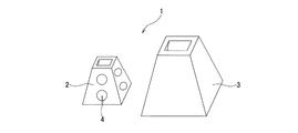
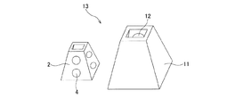
図1は、本発明の第1実施形態に係るサセプタの構成物品を別々に示した斜視図であって、(a)はバレル型の内サセプタ、(b)は外側部材である。
内サセプタ2は、凹状のザグリ部4を2つ有する台形平面4枚(台形平面4枚はすべて同面積)のそれぞれを、垂直に対し所定角度傾斜させて斜辺同士を結合させて構成され、いわゆるバレル型サセプタとなっている。
外側部材3は、内サセプタ2と略相似形状のものであり、内サセプタ2を内部に配置することができるものである。また、内サセプタ2を内部に配置したとき、内サセプタ2のザグリ部4を有する台形平面のそれぞれに対し、平行又は略平行に対向配置できる台形平面4枚(台形平面4枚はすべて同面積)を有するものである。つまり、外側部材3の台形平面は、それぞれ垂直に対し所定角度傾斜させられているものである。
また、ザグリ部4は1つ以上設けられていればよい。さらに、内サセプタ2及び外側部材3の台形平面の枚数は4枚に限らず、それぞれ3枚以上であればよい。
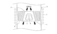
断熱材6は、サセプタ1の放熱を防止するために、反応室5の内壁とサセプタ1の外周部との間に設けられている。
高周波コイル7は、高周波を黒鉛からなるサセプタ1に加えて、サセプタ1を発熱させることができるものである。
まず、サセプタ1の内サセプタ2にエピタキシャル成長させるための基板8を載置する。次に、図2の位置に内サセプタ2を配置し、高周波コイル7を作動させて、エピタキシャル成長させるのに適切な温度にまでサセプタを加熱する。そして、反応ガスをサセプタ1の内サセプタ2と外側部材3との間を通過させる(図2の矢印参照)。
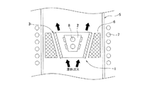
また、反応室5内の配置の変形例として、図3に示すように、図2のサセプタ1と断熱材6とを上下反転させた構成としてもよい。このとき、反応ガスを流す方向は下から上方向となる(図3の矢印参照)。
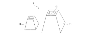
図4は、本発明の第2実施形態に係るサセプタの構成物品を別々に示した斜視図であって、(a)は内側部材、(b)はバレル型の外サセプタである。
外サセプタ11は、ザグリ部12を有する台形平面4枚(台形平面4枚はすべて同面積)のそれぞれを、垂直に対し所定角度傾斜させ、斜辺同士を結合させて構成されている。
内側部材10は、外サセプタ11と略相似形状のものであり、外サセプタ11の内部に配置することができるものである。また、内側部材10が内部に配置されたとき、外サセプタ11のザグリ部12を有する台形平面のそれぞれに対し、平行又は略平行に対向配置できる台形平面4枚(台形平面4枚はすべて同面積)を有するものである。つまり、内側部材10の台形平面は、それぞれ垂直に対し所定角度傾斜させられているものである。
また、ザグリ部12は1つ以上設けられていればよい。さらに、内サセプタ2及び外側部材3の台形平面の枚数は4枚に限らず、それぞれ3枚以上であればよい。
2 内サセプタ
3 外側部材
4 ザグリ部
5 反応室
6 断熱材
7 高周波コイル
8 基板
10 内側部材
11 外サセプタ
12 ザグリ部
Claims (6)
- 半導体エピタキシャル成長に用いられるサセプタであって、外側に複数の基板を載置自在な面を複数有するバレル型サセプタと、前記バレル型サセプタが内部に配置され、前記バレル型サセプタの前記面のそれぞれに対し同方向に傾斜して対向配置される面を有する部材とからなるサセプタ。
- 半導体エピタキシャル成長に用いられるサセプタであって、内側に複数の基板を載置自在な面を複数有するバレル型サセプタと、前記バレル型サセプタが外周部に配置され、前記バレル型サセプタの前記面のそれぞれに対し同方向に傾斜して対向配置される面を有する部材とからなるサセプタ。
- 前記部材の前記バレル型サセプタ側の面が複数の基板を載置自在である請求項1又は2に記載のサセプタ。
- 前記バレル型サセプタ又は/及び前記部材がヒーターである請求項1〜3のいずれかに記載のサセプタ。
- 黒鉛を含む基材からなる請求項1〜4のいずれかに記載のサセプタ。
- 多結晶炭化珪素又は多結晶炭化タンタルで被覆されている請求項5記載のサセプタ。
Priority Applications (8)
| Application Number | Priority Date | Filing Date | Title |
|---|---|---|---|
| JP2004106950A JP4551106B2 (ja) | 2004-03-31 | 2004-03-31 | サセプタ |
| PCT/JP2005/005675 WO2005096356A1 (ja) | 2004-03-31 | 2005-03-28 | サセプタ |
| US10/594,562 US20070186858A1 (en) | 2004-03-31 | 2005-03-28 | Susceptor |
| KR1020067019984A KR101030422B1 (ko) | 2004-03-31 | 2005-03-28 | 서셉터 |
| CA002558591A CA2558591A1 (en) | 2004-03-31 | 2005-03-28 | Susceptor |
| CNB2005800103596A CN100468631C (zh) | 2004-03-31 | 2005-03-28 | 衬托器 |
| EP05721602A EP1732111A4 (en) | 2004-03-31 | 2005-03-28 | susceptor |
| TW094110103A TW200537602A (en) | 2004-03-31 | 2005-03-30 | Susceptor |
Applications Claiming Priority (1)
| Application Number | Priority Date | Filing Date | Title |
|---|---|---|---|
| JP2004106950A JP4551106B2 (ja) | 2004-03-31 | 2004-03-31 | サセプタ |
Publications (2)
| Publication Number | Publication Date |
|---|---|
| JP2005294508A true JP2005294508A (ja) | 2005-10-20 |
| JP4551106B2 JP4551106B2 (ja) | 2010-09-22 |
Family
ID=35064063
Family Applications (1)
| Application Number | Title | Priority Date | Filing Date |
|---|---|---|---|
| JP2004106950A Expired - Fee Related JP4551106B2 (ja) | 2004-03-31 | 2004-03-31 | サセプタ |
Country Status (8)
| Country | Link |
|---|---|
| US (1) | US20070186858A1 (ja) |
| EP (1) | EP1732111A4 (ja) |
| JP (1) | JP4551106B2 (ja) |
| KR (1) | KR101030422B1 (ja) |
| CN (1) | CN100468631C (ja) |
| CA (1) | CA2558591A1 (ja) |
| TW (1) | TW200537602A (ja) |
| WO (1) | WO2005096356A1 (ja) |
Cited By (2)
| Publication number | Priority date | Publication date | Assignee | Title |
|---|---|---|---|---|
| WO2013031430A1 (ja) * | 2011-09-02 | 2013-03-07 | 東京エレクトロン株式会社 | 熱処理装置 |
| JP2020194835A (ja) * | 2019-05-27 | 2020-12-03 | 住友金属鉱山株式会社 | 炭化ケイ素多結晶膜の成膜方法、サセプタ、及び、成膜装置 |
Families Citing this family (9)
| Publication number | Priority date | Publication date | Assignee | Title |
|---|---|---|---|---|
| JP4551106B2 (ja) * | 2004-03-31 | 2010-09-22 | 東洋炭素株式会社 | サセプタ |
| US20080314319A1 (en) * | 2007-06-19 | 2008-12-25 | Memc Electronic Materials, Inc. | Susceptor for improving throughput and reducing wafer damage |
| US8404049B2 (en) * | 2007-12-27 | 2013-03-26 | Memc Electronic Materials, Inc. | Epitaxial barrel susceptor having improved thickness uniformity |
| CN102312198B (zh) * | 2010-06-30 | 2013-08-21 | 上方能源技术(杭州)有限公司 | 一种蒸镀源及蒸镀镀膜装置 |
| CN102560434B (zh) * | 2010-12-13 | 2014-10-22 | 北京北方微电子基地设备工艺研究中心有限责任公司 | 金属有机化合物化学气相沉积设备 |
| JP5880297B2 (ja) * | 2012-06-07 | 2016-03-08 | 三菱電機株式会社 | 基板支持体、半導体製造装置 |
| KR101431606B1 (ko) * | 2014-02-24 | 2014-08-22 | (주)앤피에스 | 기판 처리 장치 |
| CN106337204B (zh) * | 2015-07-17 | 2018-11-06 | 中国科学院苏州纳米技术与纳米仿生研究所 | 石墨托以及装有石墨托的晶体生长炉 |
| CN119877089B (zh) * | 2025-03-27 | 2025-06-20 | 浙江丽水中欣晶圆半导体科技有限公司 | 一种重掺磷衬底高阻值外延片生产设备 |
Citations (8)
| Publication number | Priority date | Publication date | Assignee | Title |
|---|---|---|---|---|
| JPS6332915A (ja) * | 1986-07-28 | 1988-02-12 | Furukawa Electric Co Ltd:The | 半導体気相成長装置 |
| JPH03112128A (ja) * | 1989-09-26 | 1991-05-13 | Toyoda Gosei Co Ltd | 化合物半導体の気相成長装置 |
| JPH03131017A (ja) * | 1989-10-17 | 1991-06-04 | Fujitsu Ltd | 気相成長装置 |
| JPH04241415A (ja) * | 1991-01-14 | 1992-08-28 | Furukawa Electric Co Ltd:The | 気相成長装置 |
| JPH06188195A (ja) * | 1992-12-16 | 1994-07-08 | Sumitomo Chem Co Ltd | 気相成長装置 |
| JPH11157989A (ja) * | 1997-11-25 | 1999-06-15 | Toyo Tanso Kk | 気相成長用サセプター及びその製造方法 |
| JPH11176757A (ja) * | 1997-12-11 | 1999-07-02 | Shimada Phys & Chem Ind Co Ltd | バレル型気相成長装置 |
| JP2001122692A (ja) * | 1999-10-26 | 2001-05-08 | Central Res Inst Of Electric Power Ind | 半導体結晶の製造方法およびこれを利用する製造装置 |
Family Cites Families (6)
| Publication number | Priority date | Publication date | Assignee | Title |
|---|---|---|---|---|
| US4099041A (en) * | 1977-04-11 | 1978-07-04 | Rca Corporation | Susceptor for heating semiconductor substrates |
| JPH01125923A (ja) * | 1987-11-11 | 1989-05-18 | Sumitomo Chem Co Ltd | 気相成長装置 |
| US5104690A (en) * | 1990-06-06 | 1992-04-14 | Spire Corporation | CVD thin film compounds |
| US6217662B1 (en) * | 1997-03-24 | 2001-04-17 | Cree, Inc. | Susceptor designs for silicon carbide thin films |
| IL125690A0 (en) * | 1998-08-06 | 1999-04-11 | Reiser Raphael Joshua | Furnace for processing semiconductor wafers |
| JP4551106B2 (ja) * | 2004-03-31 | 2010-09-22 | 東洋炭素株式会社 | サセプタ |
-
2004
- 2004-03-31 JP JP2004106950A patent/JP4551106B2/ja not_active Expired - Fee Related
-
2005
- 2005-03-28 CA CA002558591A patent/CA2558591A1/en not_active Abandoned
- 2005-03-28 KR KR1020067019984A patent/KR101030422B1/ko not_active Expired - Fee Related
- 2005-03-28 EP EP05721602A patent/EP1732111A4/en not_active Withdrawn
- 2005-03-28 CN CNB2005800103596A patent/CN100468631C/zh not_active Expired - Fee Related
- 2005-03-28 US US10/594,562 patent/US20070186858A1/en not_active Abandoned
- 2005-03-28 WO PCT/JP2005/005675 patent/WO2005096356A1/ja not_active Ceased
- 2005-03-30 TW TW094110103A patent/TW200537602A/zh not_active IP Right Cessation
Patent Citations (8)
| Publication number | Priority date | Publication date | Assignee | Title |
|---|---|---|---|---|
| JPS6332915A (ja) * | 1986-07-28 | 1988-02-12 | Furukawa Electric Co Ltd:The | 半導体気相成長装置 |
| JPH03112128A (ja) * | 1989-09-26 | 1991-05-13 | Toyoda Gosei Co Ltd | 化合物半導体の気相成長装置 |
| JPH03131017A (ja) * | 1989-10-17 | 1991-06-04 | Fujitsu Ltd | 気相成長装置 |
| JPH04241415A (ja) * | 1991-01-14 | 1992-08-28 | Furukawa Electric Co Ltd:The | 気相成長装置 |
| JPH06188195A (ja) * | 1992-12-16 | 1994-07-08 | Sumitomo Chem Co Ltd | 気相成長装置 |
| JPH11157989A (ja) * | 1997-11-25 | 1999-06-15 | Toyo Tanso Kk | 気相成長用サセプター及びその製造方法 |
| JPH11176757A (ja) * | 1997-12-11 | 1999-07-02 | Shimada Phys & Chem Ind Co Ltd | バレル型気相成長装置 |
| JP2001122692A (ja) * | 1999-10-26 | 2001-05-08 | Central Res Inst Of Electric Power Ind | 半導体結晶の製造方法およびこれを利用する製造装置 |
Non-Patent Citations (1)
| Title |
|---|
| BARBARA E. LANDINI: "Susceptor Effects on the Morphological and Impurity Properties of 4H-SiC Epilayers", JOURNAL OF ELECTRONIC MATERIALS, vol. 29, no. 3, JPN6009034521, 2000, pages 384 - 390, XP002989573, ISSN: 0001365567 * |
Cited By (4)
| Publication number | Priority date | Publication date | Assignee | Title |
|---|---|---|---|---|
| WO2013031430A1 (ja) * | 2011-09-02 | 2013-03-07 | 東京エレクトロン株式会社 | 熱処理装置 |
| JP2013055201A (ja) * | 2011-09-02 | 2013-03-21 | Tokyo Electron Ltd | 熱処理装置 |
| JP2020194835A (ja) * | 2019-05-27 | 2020-12-03 | 住友金属鉱山株式会社 | 炭化ケイ素多結晶膜の成膜方法、サセプタ、及び、成膜装置 |
| JP7247749B2 (ja) | 2019-05-27 | 2023-03-29 | 住友金属鉱山株式会社 | 炭化ケイ素多結晶膜の成膜方法、サセプタ、及び、成膜装置 |
Also Published As
| Publication number | Publication date |
|---|---|
| TW200537602A (en) | 2005-11-16 |
| WO2005096356A1 (ja) | 2005-10-13 |
| EP1732111A1 (en) | 2006-12-13 |
| EP1732111A4 (en) | 2009-11-04 |
| US20070186858A1 (en) | 2007-08-16 |
| JP4551106B2 (ja) | 2010-09-22 |
| CN1938822A (zh) | 2007-03-28 |
| KR101030422B1 (ko) | 2011-04-20 |
| CA2558591A1 (en) | 2005-10-13 |
| TWI376730B (ja) | 2012-11-11 |
| CN100468631C (zh) | 2009-03-11 |
| KR20060131921A (ko) | 2006-12-20 |
Similar Documents
| Publication | Publication Date | Title |
|---|---|---|
| US20120231615A1 (en) | Semiconductor thin-film manufacturing method, semiconductor thin-film manufacturing apparatus, susceptor, and susceptor holder | |
| JP7419779B2 (ja) | サセプタ及び化学気相成長装置 | |
| JP2008060545A (ja) | 半導体製造装置および半導体製造方法 | |
| JP7190894B2 (ja) | SiC化学気相成長装置 | |
| JP4551106B2 (ja) | サセプタ | |
| TWI681070B (zh) | 氣相成長方法 | |
| US20080124901A1 (en) | Method for maintaining semiconductor manufacturing apparatus, semiconductor manufacturing apparatus, and method for manufacturing semiconductor | |
| JP7694744B2 (ja) | SiCデバイス及びSiCデバイスの製造方法 | |
| JP2015146416A (ja) | 炭化珪素基板用支持部材、炭化珪素成長装置用部材、および炭化珪素エピタキシャル基板の製造方法 | |
| JP2020100528A (ja) | 積層体、積層体の製造方法および炭化珪素多結晶基板の製造方法 | |
| JP2023042593A (ja) | SiCエピタキシャルウェハ | |
| JP5100231B2 (ja) | Iii族窒化物製造装置 | |
| JP7413768B2 (ja) | 多結晶基板の製造方法 | |
| JP7220845B2 (ja) | サセプタ、サセプタの再生方法、及び、成膜方法 | |
| JP7294021B2 (ja) | 黒鉛製支持基板の表面処理方法、炭化珪素多結晶膜の成膜方法および炭化珪素多結晶基板の製造方法 | |
| JP7296914B2 (ja) | サテライトおよび炭化珪素半導体装置の製造方法 | |
| WO2020158657A1 (ja) | 成膜装置及び成膜方法 | |
| JP2025078074A (ja) | SiCエピタキシャルウェハ | |
| JP2025078071A (ja) | SiCエピタキシャルウェハ | |
| JP2025078072A (ja) | SiCエピタキシャルウェハ | |
| JP2021103720A (ja) | エピタキシャル膜成長用ウエハ、エピタキシャル膜成長方法、除去方法、および、エピタキシャルウエハの製造方法 | |
| JP2008198857A (ja) | 半導体製造装置 |
Legal Events
| Date | Code | Title | Description |
|---|---|---|---|
| A621 | Written request for application examination |
Free format text: JAPANESE INTERMEDIATE CODE: A621 Effective date: 20061211 |
|
| A131 | Notification of reasons for refusal |
Free format text: JAPANESE INTERMEDIATE CODE: A131 Effective date: 20090714 |
|
| A521 | Request for written amendment filed |
Free format text: JAPANESE INTERMEDIATE CODE: A523 Effective date: 20090914 |
|
| A131 | Notification of reasons for refusal |
Free format text: JAPANESE INTERMEDIATE CODE: A131 Effective date: 20091222 |
|
| A521 | Request for written amendment filed |
Free format text: JAPANESE INTERMEDIATE CODE: A523 Effective date: 20100222 |
|
| TRDD | Decision of grant or rejection written | ||
| A01 | Written decision to grant a patent or to grant a registration (utility model) |
Free format text: JAPANESE INTERMEDIATE CODE: A01 Effective date: 20100706 |
|
| A01 | Written decision to grant a patent or to grant a registration (utility model) |
Free format text: JAPANESE INTERMEDIATE CODE: A01 |
|
| A61 | First payment of annual fees (during grant procedure) |
Free format text: JAPANESE INTERMEDIATE CODE: A61 Effective date: 20100709 |
|
| R150 | Certificate of patent or registration of utility model |
Free format text: JAPANESE INTERMEDIATE CODE: R150 |
|
| FPAY | Renewal fee payment (event date is renewal date of database) |
Free format text: PAYMENT UNTIL: 20130716 Year of fee payment: 3 |
|
| LAPS | Cancellation because of no payment of annual fees |