JP2005291865A - 電源電圧監視回路 - Google Patents
電源電圧監視回路 Download PDFInfo
- Publication number
- JP2005291865A JP2005291865A JP2004106184A JP2004106184A JP2005291865A JP 2005291865 A JP2005291865 A JP 2005291865A JP 2004106184 A JP2004106184 A JP 2004106184A JP 2004106184 A JP2004106184 A JP 2004106184A JP 2005291865 A JP2005291865 A JP 2005291865A
- Authority
- JP
- Japan
- Prior art keywords
- voltage
- power supply
- supply voltage
- circuit
- output
- Prior art date
- Legal status (The legal status is an assumption and is not a legal conclusion. Google has not performed a legal analysis and makes no representation as to the accuracy of the status listed.)
- Granted
Links
- 238000012544 monitoring process Methods 0.000 title claims abstract description 51
- 239000003990 capacitor Substances 0.000 claims description 2
- 230000007257 malfunction Effects 0.000 abstract description 7
- 229910044991 metal oxide Inorganic materials 0.000 abstract description 2
- 150000004706 metal oxides Chemical class 0.000 abstract description 2
- 239000004065 semiconductor Substances 0.000 abstract description 2
- 238000001514 detection method Methods 0.000 description 15
- 238000010586 diagram Methods 0.000 description 6
- 230000000052 comparative effect Effects 0.000 description 1
- 238000000034 method Methods 0.000 description 1
- 230000000630 rising effect Effects 0.000 description 1
Images
Classifications
-
- G—PHYSICS
- G05—CONTROLLING; REGULATING
- G05F—SYSTEMS FOR REGULATING ELECTRIC OR MAGNETIC VARIABLES
- G05F3/00—Non-retroactive systems for regulating electric variables by using an uncontrolled element, or an uncontrolled combination of elements, such element or such combination having self-regulating properties
- G05F3/02—Regulating voltage or current
- G05F3/08—Regulating voltage or current wherein the variable is DC
- G05F3/10—Regulating voltage or current wherein the variable is DC using uncontrolled devices with non-linear characteristics
- G05F3/16—Regulating voltage or current wherein the variable is DC using uncontrolled devices with non-linear characteristics being semiconductor devices
- G05F3/20—Regulating voltage or current wherein the variable is DC using uncontrolled devices with non-linear characteristics being semiconductor devices using diode- transistor combinations
- G05F3/26—Current mirrors
- G05F3/262—Current mirrors using field-effect transistors only
-
- H—ELECTRICITY
- H03—ELECTRONIC CIRCUITRY
- H03K—PULSE TECHNIQUE
- H03K17/00—Electronic switching or gating, i.e. not by contact-making and –breaking
- H03K17/22—Modifications for ensuring a predetermined initial state when the supply voltage has been applied
- H03K17/223—Modifications for ensuring a predetermined initial state when the supply voltage has been applied in field-effect transistor switches
Landscapes
- Engineering & Computer Science (AREA)
- Microelectronics & Electronic Packaging (AREA)
- Physics & Mathematics (AREA)
- Nonlinear Science (AREA)
- Electromagnetism (AREA)
- General Physics & Mathematics (AREA)
- Radar, Positioning & Navigation (AREA)
- Automation & Control Theory (AREA)
- Measurement Of Current Or Voltage (AREA)
Abstract
比較誤動作を抑制することが可能な電源電圧監視回路を提供すること。
【解決手段】
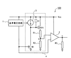
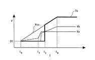
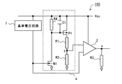
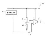
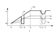
本発明にかかる電源電圧監視回路では、P型MOSトランジスタP1のドレインが電源電圧Vccと接続され、ソースがコンパレータ2の入力端子と分圧回路R1、R2を介して接続されている。またN型MOSトランジスタN1のゲートには、基準電圧回路1より出力された出力電圧が入力され、ドレインはP型MOSトランジスタP1のゲートに接続されている。N型MOSトランジスタN1は、ゲートに入力された電圧が基準電圧に到達した場合にオン状態になる。これに応じてP型MOSトランジスタP1もオン状態になり、コンパレータ2に電源電圧Vccに応じた電圧が供給され、比較動作が行われる。
【選択図】 図1
Description
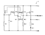
P型MOSトランジスタP13およびP14のゲートとドレインとが互に接続されている。N型MOSトランジスタN11のゲートとドレインとN型MOSトランジスタN12のゲートとが互いに接続される。P型MOSトランジスタP13およびP14のゲートとP型MOSトランジスタP14のドレインの接続点は、図1に示す電流源3に接続されているとともに、P型MOSトランジスタP15のゲートに接続されている。このP型MOSトランジスタP15と抵抗R13と、この抵抗R13側をアノードとするダイオードD11とが電源電位Vccおよび接地電位GND間に直列接続で挿入され、この直列接続点の電圧が図1に示すN型MOSトランジスタN1に接続されている。
さらにP型MOSトランジスタP13と並列にP型MOSトランジスタP12が接続され、そのゲートはP型MOSトランジスタP11のドレインと接続されている。また、電源電位Vccと接地電位GNDとの間にP型MOSトランジスタP11と抵抗R11が直列接続で挿入され、P型MOSトランジスタP11のドレインは容量素子C11を介して接地電位に接続される。
図1に示す例では、電流源3を用いたが、電流源3の代りに図4に示すように抵抗R4を設けるようにしてもよい。尚、抵抗R4は、消費電力の増大を抑制するために高抵抗であることが望ましい。
2 コンパレータ
3 電流源
Claims (10)
- 自己電源電圧を監視する電源電圧監視回路であって、
電源電圧が入力され、当該電源電圧に応じて基準電圧を生成し出力する基準電圧回路と、
前記基準電圧回路から出力された出力電圧と、前記電源電圧に応じて変化する電圧を入力し、両者を比較して、その比較結果を出力するコンパレータと、
前記基準電圧回路から出力された出力電圧が基準電圧に到達する前に、前記電源電圧に応じた電圧が前記コンパレータに入力されないように制御する制御手段とを備えた電源電圧監視回路。 - 自己電源電圧を監視する電源電圧監視回路であって、
電源電圧が入力され、当該電源電圧に応じて基準電圧を生成し出力する基準電圧回路と、
前記基準電圧回路から出力された出力電圧と、前記電源電圧に応じて変化する電圧を入力し、両者を比較して、その比較結果を出力するコンパレータと、
前記電源電圧と前記コンパレータ間の導通を制御する第1のスイッチ手段と、
前記基準電圧回路より出力された出力電圧を入力し、当該出力電圧に応じて前記第1のスイッチ手段を制御する第2のスイッチ手段とを備え、
前記第2のスイッチ手段は、前記基準電圧回路から出力された出力電圧が基準電圧に到達する前には、前記電源電圧に応じた電圧が前記コンパレータに入力されないように前記第1のスイッチ手段を制御する電源電圧監視回路。 - 自己電源電圧を監視する電源電圧監視回路であって、
電源電圧が入力され、当該電源電圧に応じて基準電圧を生成し出力する基準電圧回路と、
第1の入力端子より入力された電圧と、第2の入力端子より入力された電圧を比較して、その比較結果を出力するコンパレータと、
前記電源電圧と前記コンパレータ間の導通を制御する第1のトランジスタと、
前記基準電圧回路より出力された出力電圧をゲートに入力し、ドレインが前記第1のトランジスタのゲートに接続された第2のトランジスタとを備え、
前記コンパレータの第1の入力端子には前記第1のトランジスタによって導通が制御された電圧が入力され、前記第2の入力端子には、前記基準電圧回路より出力された出力電圧が入力され、
前記第2のトランジスタは、前記基準電圧回路から出力された出力電圧が基準電圧に到達する前には、前記電源電圧に応じた電圧が前記コンパレータに入力されないように前記第1のトランジスタのゲートに電圧を供給する電源電圧監視回路。 - 前記第1のトランジスタのゲートと、前記第2のトランジスタのドレインとの間に、基準電圧回路より生成される電流源からの電流を供給したことを特徴とする請求項3記載の電源電圧監視回路。
- 前記第1のトランジスタのゲートと、前記第2のトランジスタのドレインとの接続点を、前記電源電圧と接続された抵抗と接続したことを特徴とする請求項3記載の電源電圧監視回路。
- 前記第1のトランジスタのゲートと、前記第2のトランジスタのドレインとの接続点を、前記電源電圧と接続された容量素子と接続したことを特徴とする請求項4又は5記載の電源電圧監視回路。
- 自己電源電圧を監視する電源電圧監視回路であって、
電源電圧が入力され、当該電源電圧に応じて基準電圧を生成し出力する基準電圧回路と、
第1の入力端子より入力された電圧と、第2の入力端子に前記基準電圧回路から入力された電圧を比較して、その比較結果を出力するコンパレータと、
ドレインが前記電源電圧と接続され、ソースが前記コンパレータの第1の入力端子と分圧回路を介して接続されたP型MOSトランジスタと、
前記基準電圧回路より出力された出力電圧をゲートに入力し、ドレインが前記P型MOSトランジスタのゲートに接続され、ソースが接地され、前記ゲートに入力された電圧が基準電圧に到達した場合にオン状態になるN型MOSトランジスタとを備えた電源電圧監視回路。 - 前記P型MOSトランジスタのゲートと、前記N型MOSトランジスタのドレインとの間に、基準電圧回路より生成される電流源からの電流を供給したことを特徴とする請求項7記載の電源電圧監視回路。
- 前記P型MOSトランジスタのゲートと、前記N型MOSトランジスタのドレインとの接続点を、前記電源電圧と接続された抵抗と接続したことを特徴とする請求項7記載の電源電圧監視回路。
- 前記P型MOSトランジスタのゲートと、前記N型MOSトランジスタのドレインとの接続点を、前記電源電圧と接続された容量素子と接続したことを特徴とする請求項8又は9記載の電源電圧監視回路。
Priority Applications (2)
| Application Number | Priority Date | Filing Date | Title |
|---|---|---|---|
| JP2004106184A JP4439974B2 (ja) | 2004-03-31 | 2004-03-31 | 電源電圧監視回路 |
| US11/085,132 US7274226B2 (en) | 2004-03-31 | 2005-03-22 | Power source voltage monitoring circuit for self-monitoring its power source voltage |
Applications Claiming Priority (1)
| Application Number | Priority Date | Filing Date | Title |
|---|---|---|---|
| JP2004106184A JP4439974B2 (ja) | 2004-03-31 | 2004-03-31 | 電源電圧監視回路 |
Publications (2)
| Publication Number | Publication Date |
|---|---|
| JP2005291865A true JP2005291865A (ja) | 2005-10-20 |
| JP4439974B2 JP4439974B2 (ja) | 2010-03-24 |
Family
ID=35053605
Family Applications (1)
| Application Number | Title | Priority Date | Filing Date |
|---|---|---|---|
| JP2004106184A Expired - Fee Related JP4439974B2 (ja) | 2004-03-31 | 2004-03-31 | 電源電圧監視回路 |
Country Status (2)
| Country | Link |
|---|---|
| US (1) | US7274226B2 (ja) |
| JP (1) | JP4439974B2 (ja) |
Cited By (6)
| Publication number | Priority date | Publication date | Assignee | Title |
|---|---|---|---|---|
| JP2007121088A (ja) * | 2005-10-27 | 2007-05-17 | Sanyo Electric Co Ltd | 低電圧検出回路 |
| JP2010223796A (ja) * | 2009-03-24 | 2010-10-07 | Renesas Electronics Corp | 電源電圧検出回路 |
| WO2013128802A1 (ja) * | 2012-02-28 | 2013-09-06 | パナソニック株式会社 | 電圧検出回路 |
| JP2013219454A (ja) * | 2012-04-05 | 2013-10-24 | Renesas Electronics Corp | パワーオン・リセット回路及び半導体装置 |
| US10879891B2 (en) | 2019-05-16 | 2020-12-29 | Jtekt Corporation | Power supply voltage monitoring circuit and control device |
| US11476840B2 (en) | 2020-09-01 | 2022-10-18 | Samsung Sdi Co., Ltd. | Comparator circuit and switch control device including the same |
Families Citing this family (7)
| Publication number | Priority date | Publication date | Assignee | Title |
|---|---|---|---|---|
| US8850232B2 (en) * | 2008-03-19 | 2014-09-30 | Freescale Semiconductor, Inc. | Method for protecting a cryptographic module and a device having cryptographic module protection capabilities |
| JP2010166110A (ja) * | 2009-01-13 | 2010-07-29 | Seiko Instruments Inc | 電圧検出回路 |
| US8823418B2 (en) * | 2009-09-17 | 2014-09-02 | Taiwan Semiconductor Manufacturing Co., Ltd. | Power on detection circuit |
| JP5433510B2 (ja) * | 2010-06-23 | 2014-03-05 | 株式会社東芝 | 電源電圧監視回路 |
| US9046570B2 (en) | 2012-08-03 | 2015-06-02 | Freescale Semiconductor, Inc. | Method and apparatus for limiting access to an integrated circuit (IC) |
| US8988114B2 (en) | 2012-11-20 | 2015-03-24 | Freescale Semiconductor, Inc. | Low-power voltage tamper detection |
| US20140145695A1 (en) * | 2012-11-26 | 2014-05-29 | Nxp B.V. | Startup control circuit in voltage regulators and related circuits |
Family Cites Families (5)
| Publication number | Priority date | Publication date | Assignee | Title |
|---|---|---|---|---|
| JPS5914383A (ja) * | 1982-07-14 | 1984-01-25 | Matsushita Electric Ind Co Ltd | 直流モ−タのスイツチングガバナ装置 |
| US4712477A (en) * | 1985-06-10 | 1987-12-15 | Asahi Kasei Kogyo Kabushiki Kaisha | Electronic delay detonator |
| US5455469A (en) * | 1993-10-12 | 1995-10-03 | Watsco Components, Inc. | Comparator controlled delay-on-break devices |
| JPH09135157A (ja) | 1995-11-10 | 1997-05-20 | Nec Corp | パワーオンリセット回路 |
| FR2767589B1 (fr) * | 1997-08-21 | 2000-07-21 | Sgs Thomson Microelectronics | Dispositif de surveillance de tension d'alimentation de type "reset" |
-
2004
- 2004-03-31 JP JP2004106184A patent/JP4439974B2/ja not_active Expired - Fee Related
-
2005
- 2005-03-22 US US11/085,132 patent/US7274226B2/en not_active Expired - Fee Related
Cited By (9)
| Publication number | Priority date | Publication date | Assignee | Title |
|---|---|---|---|---|
| JP2007121088A (ja) * | 2005-10-27 | 2007-05-17 | Sanyo Electric Co Ltd | 低電圧検出回路 |
| JP2010223796A (ja) * | 2009-03-24 | 2010-10-07 | Renesas Electronics Corp | 電源電圧検出回路 |
| US8373405B2 (en) | 2009-03-24 | 2013-02-12 | Renesas Electronics Corporation | Power supply voltage detection circuit |
| WO2013128802A1 (ja) * | 2012-02-28 | 2013-09-06 | パナソニック株式会社 | 電圧検出回路 |
| JPWO2013128802A1 (ja) * | 2012-02-28 | 2015-07-30 | パナソニックIpマネジメント株式会社 | 電圧検出回路 |
| US9236857B2 (en) | 2012-02-28 | 2016-01-12 | Panasonic Intellectual Property Management Co., Ltd. | Voltage detection circuit |
| JP2013219454A (ja) * | 2012-04-05 | 2013-10-24 | Renesas Electronics Corp | パワーオン・リセット回路及び半導体装置 |
| US10879891B2 (en) | 2019-05-16 | 2020-12-29 | Jtekt Corporation | Power supply voltage monitoring circuit and control device |
| US11476840B2 (en) | 2020-09-01 | 2022-10-18 | Samsung Sdi Co., Ltd. | Comparator circuit and switch control device including the same |
Also Published As
| Publication number | Publication date |
|---|---|
| US20050218969A1 (en) | 2005-10-06 |
| JP4439974B2 (ja) | 2010-03-24 |
| US7274226B2 (en) | 2007-09-25 |
Similar Documents
| Publication | Publication Date | Title |
|---|---|---|
| JP5421133B2 (ja) | ボルテージレギュレータ | |
| JP5315026B2 (ja) | 半導体装置 | |
| CN102854908B (zh) | 调节器用半导体集成电路 | |
| JP5148537B2 (ja) | 電源電圧検出回路 | |
| US20080007325A1 (en) | Current source circuit | |
| JP2009169785A (ja) | ボルテージレギュレータ | |
| JP4439974B2 (ja) | 電源電圧監視回路 | |
| US8482891B2 (en) | Electrostatic discharge protection circuit | |
| KR20140104352A (ko) | 레벨 시프트 회로 | |
| JP5123679B2 (ja) | 基準電圧生成回路及びその起動制御方法 | |
| JP4981267B2 (ja) | 過熱検出回路 | |
| JP2009277122A (ja) | 電源電圧監視回路 | |
| JP5637096B2 (ja) | バンドギャップ基準電圧回路及びこれを用いたパワーオンリセット回路 | |
| JP6926982B2 (ja) | 電源制御回路および環境発電装置 | |
| JP5889700B2 (ja) | パワーオン・リセット回路及び半導体装置 | |
| JP2005293067A (ja) | ボルテージレギュレータ | |
| JP2008197994A (ja) | 起動回路 | |
| JP4295289B2 (ja) | 基準電源電圧回路 | |
| JP4666636B2 (ja) | スイッチング素子駆動回路装置及びそれを用いた電子機器 | |
| JP4594064B2 (ja) | サージ電流抑制回路及び直流電源装置 | |
| JP2010153974A (ja) | コンパレータ及び検出回路 | |
| JP2006039812A (ja) | 直流安定化電源回路 | |
| JP4147174B2 (ja) | パワーオンリセット回路 | |
| JP5687091B2 (ja) | 電源電圧検出回路 | |
| JP2017041139A (ja) | Ldo回路 |
Legal Events
| Date | Code | Title | Description |
|---|---|---|---|
| A621 | Written request for application examination |
Free format text: JAPANESE INTERMEDIATE CODE: A621 Effective date: 20070206 |
|
| A977 | Report on retrieval |
Free format text: JAPANESE INTERMEDIATE CODE: A971007 Effective date: 20090713 |
|
| A131 | Notification of reasons for refusal |
Free format text: JAPANESE INTERMEDIATE CODE: A131 Effective date: 20090721 |
|
| A521 | Request for written amendment filed |
Free format text: JAPANESE INTERMEDIATE CODE: A523 Effective date: 20090918 |
|
| A131 | Notification of reasons for refusal |
Free format text: JAPANESE INTERMEDIATE CODE: A131 Effective date: 20091013 |
|
| A521 | Request for written amendment filed |
Free format text: JAPANESE INTERMEDIATE CODE: A523 Effective date: 20091118 |
|
| TRDD | Decision of grant or rejection written | ||
| A01 | Written decision to grant a patent or to grant a registration (utility model) |
Free format text: JAPANESE INTERMEDIATE CODE: A01 Effective date: 20091208 |
|
| A01 | Written decision to grant a patent or to grant a registration (utility model) |
Free format text: JAPANESE INTERMEDIATE CODE: A01 |
|
| A61 | First payment of annual fees (during grant procedure) |
Free format text: JAPANESE INTERMEDIATE CODE: A61 Effective date: 20100106 |
|
| FPAY | Renewal fee payment (event date is renewal date of database) |
Free format text: PAYMENT UNTIL: 20130115 Year of fee payment: 3 |
|
| R150 | Certificate of patent or registration of utility model |
Free format text: JAPANESE INTERMEDIATE CODE: R150 |
|
| FPAY | Renewal fee payment (event date is renewal date of database) |
Free format text: PAYMENT UNTIL: 20130115 Year of fee payment: 3 |
|
| S533 | Written request for registration of change of name |
Free format text: JAPANESE INTERMEDIATE CODE: R313533 |
|
| FPAY | Renewal fee payment (event date is renewal date of database) |
Free format text: PAYMENT UNTIL: 20130115 Year of fee payment: 3 |
|
| R350 | Written notification of registration of transfer |
Free format text: JAPANESE INTERMEDIATE CODE: R350 |
|
| FPAY | Renewal fee payment (event date is renewal date of database) |
Free format text: PAYMENT UNTIL: 20130115 Year of fee payment: 3 |
|
| FPAY | Renewal fee payment (event date is renewal date of database) |
Free format text: PAYMENT UNTIL: 20140115 Year of fee payment: 4 |
|
| S531 | Written request for registration of change of domicile |
Free format text: JAPANESE INTERMEDIATE CODE: R313531 |
|
| R350 | Written notification of registration of transfer |
Free format text: JAPANESE INTERMEDIATE CODE: R350 |
|
| LAPS | Cancellation because of no payment of annual fees |