JP2005267734A - 昇圧回路及びそれを用いた不揮発性メモリ - Google Patents
昇圧回路及びそれを用いた不揮発性メモリ Download PDFInfo
- Publication number
- JP2005267734A JP2005267734A JP2004077757A JP2004077757A JP2005267734A JP 2005267734 A JP2005267734 A JP 2005267734A JP 2004077757 A JP2004077757 A JP 2004077757A JP 2004077757 A JP2004077757 A JP 2004077757A JP 2005267734 A JP2005267734 A JP 2005267734A
- Authority
- JP
- Japan
- Prior art keywords
- booster circuit
- circuit
- stages
- basic pump
- voltage
- Prior art date
- Legal status (The legal status is an assumption and is not a legal conclusion. Google has not performed a legal analysis and makes no representation as to the accuracy of the status listed.)
- Pending
Links
- 230000015654 memory Effects 0.000 title claims abstract description 36
- 239000004065 semiconductor Substances 0.000 claims abstract description 9
- 238000001514 detection method Methods 0.000 claims description 14
- LPQOADBMXVRBNX-UHFFFAOYSA-N ac1ldcw0 Chemical group Cl.C1CN(C)CCN1C1=C(F)C=C2C(=O)C(C(O)=O)=CN3CCSC1=C32 LPQOADBMXVRBNX-UHFFFAOYSA-N 0.000 claims 1
- 239000011159 matrix material Substances 0.000 claims 1
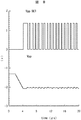
- 238000004088 simulation Methods 0.000 description 7
- 230000000694 effects Effects 0.000 description 5
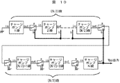
- 238000010586 diagram Methods 0.000 description 4
- 229910044991 metal oxide Inorganic materials 0.000 description 2
- 239000000758 substrate Substances 0.000 description 2
- -1 Metal Oxide Nitride Chemical class 0.000 description 1
- 239000002784 hot electron Substances 0.000 description 1
- 230000014759 maintenance of location Effects 0.000 description 1
- 238000005259 measurement Methods 0.000 description 1
- 150000004706 metal oxides Chemical class 0.000 description 1
- 238000000034 method Methods 0.000 description 1
- 230000002093 peripheral effect Effects 0.000 description 1
- 230000004044 response Effects 0.000 description 1
- 230000000630 rising effect Effects 0.000 description 1
Images


Classifications
-
- G—PHYSICS
- G11—INFORMATION STORAGE
- G11C—STATIC STORES
- G11C16/00—Erasable programmable read-only memories
- G11C16/02—Erasable programmable read-only memories electrically programmable
- G11C16/06—Auxiliary circuits, e.g. for writing into memory
- G11C16/10—Programming or data input circuits
- G11C16/12—Programming voltage switching circuits
Landscapes
- Read Only Memory (AREA)
- Dc-Dc Converters (AREA)
Priority Applications (3)
| Application Number | Priority Date | Filing Date | Title |
|---|---|---|---|
| JP2004077757A JP2005267734A (ja) | 2004-03-18 | 2004-03-18 | 昇圧回路及びそれを用いた不揮発性メモリ |
| US11/050,753 US7221610B2 (en) | 2004-03-18 | 2005-02-07 | Charge pump circuit for generating high voltages required in read/write/erase/standby modes in non-volatile memory device |
| CN200510009456.5A CN1670864A (zh) | 2004-03-18 | 2005-02-08 | 升压电路和使用了它的非易失性存储器 |
Applications Claiming Priority (1)
| Application Number | Priority Date | Filing Date | Title |
|---|---|---|---|
| JP2004077757A JP2005267734A (ja) | 2004-03-18 | 2004-03-18 | 昇圧回路及びそれを用いた不揮発性メモリ |
Publications (2)
| Publication Number | Publication Date |
|---|---|
| JP2005267734A true JP2005267734A (ja) | 2005-09-29 |
| JP2005267734A5 JP2005267734A5 (enExample) | 2006-08-24 |
Family
ID=34986097
Family Applications (1)
| Application Number | Title | Priority Date | Filing Date |
|---|---|---|---|
| JP2004077757A Pending JP2005267734A (ja) | 2004-03-18 | 2004-03-18 | 昇圧回路及びそれを用いた不揮発性メモリ |
Country Status (3)
| Country | Link |
|---|---|
| US (1) | US7221610B2 (enExample) |
| JP (1) | JP2005267734A (enExample) |
| CN (1) | CN1670864A (enExample) |
Cited By (4)
| Publication number | Priority date | Publication date | Assignee | Title |
|---|---|---|---|---|
| US7212441B2 (en) | 2004-12-28 | 2007-05-01 | Renesas Technology Corporation | Non volatile semiconductor memory device |
| JP2008269727A (ja) * | 2007-04-24 | 2008-11-06 | Matsushita Electric Ind Co Ltd | 昇圧回路、半導体記憶装置およびその駆動方法 |
| JP2011216136A (ja) * | 2010-03-31 | 2011-10-27 | Fujitsu Semiconductor Ltd | 半導体集積回路装置 |
| JP2014183735A (ja) * | 2013-03-15 | 2014-09-29 | Freescale Semiconductor Inc | 負電荷ポンプ調整 |
Families Citing this family (14)
| Publication number | Priority date | Publication date | Assignee | Title |
|---|---|---|---|---|
| KR100699872B1 (ko) * | 2005-11-02 | 2007-03-28 | 삼성전자주식회사 | 전압 펌프의 수를 조절할 수 있는 상 변화 메모리 장치 및기입 구동 전압 발생 방법 |
| JP4851903B2 (ja) * | 2005-11-08 | 2012-01-11 | 株式会社東芝 | 半導体チャージポンプ |
| US7430676B2 (en) * | 2006-03-03 | 2008-09-30 | Apple, Inc. | Method and apparatus for changing the clock frequency of a memory system |
| JP4829029B2 (ja) | 2006-08-02 | 2011-11-30 | 株式会社東芝 | メモリシステム及びメモリチップ |
| KR100809071B1 (ko) * | 2006-09-25 | 2008-03-03 | 삼성전자주식회사 | 고전압 발생 회로를 구비하는 반도체 장치 및 그 전압 발생방법 |
| KR100809072B1 (ko) * | 2006-09-28 | 2008-03-03 | 삼성전자주식회사 | 고전압 발생 회로를 구비하는 반도체 장치 및 그 전압 발생방법 |
| US8189396B2 (en) | 2006-12-14 | 2012-05-29 | Mosaid Technologies Incorporated | Word line driver in a hierarchical NOR flash memory |
| US20090066407A1 (en) * | 2007-09-12 | 2009-03-12 | Rochester Institute Of Technology | Charge pump systems and methods thereof |
| KR20120068228A (ko) * | 2010-12-17 | 2012-06-27 | 에스케이하이닉스 주식회사 | 반도체 장치 및 그 동작방법 |
| US9177616B2 (en) * | 2012-10-04 | 2015-11-03 | Cypress Semiconductor Corporation | Supply power dependent controllable write throughput for memory applications |
| CN104682693B (zh) * | 2013-12-02 | 2017-12-05 | 北京兆易创新科技股份有限公司 | 一种升压电路和非易失性存储器 |
| US9449655B1 (en) | 2015-08-31 | 2016-09-20 | Cypress Semiconductor Corporation | Low standby power with fast turn on for non-volatile memory devices |
| US10283207B2 (en) | 2016-06-03 | 2019-05-07 | Samsung Electronics Co., Ltd. | Non-volatile memory devices comprising high voltage generation circuits and operating methods thereof |
| US11908528B2 (en) | 2020-11-20 | 2024-02-20 | Stmicroelectronics International N.V. | Selectively configurable charge pump |
Family Cites Families (9)
| Publication number | Priority date | Publication date | Assignee | Title |
|---|---|---|---|---|
| JPS6095794A (ja) | 1983-10-28 | 1985-05-29 | Hitachi Ltd | 半導体集積回路 |
| JPH0666114B2 (ja) | 1984-09-21 | 1994-08-24 | 株式会社日立製作所 | 半導体集積回路 |
| US5602794A (en) * | 1995-09-29 | 1997-02-11 | Intel Corporation | Variable stage charge pump |
| JP3223504B2 (ja) * | 1998-03-31 | 2001-10-29 | 日本電気株式会社 | 昇圧回路 |
| US6151229A (en) * | 1999-06-30 | 2000-11-21 | Intel Corporation | Charge pump with gated pumped output diode at intermediate stage |
| US6927441B2 (en) * | 2001-03-20 | 2005-08-09 | Stmicroelectronics S.R.L. | Variable stage charge pump |
| JP4336489B2 (ja) | 2002-11-18 | 2009-09-30 | 株式会社ルネサステクノロジ | 半導体集積回路 |
| JP4223270B2 (ja) | 2002-11-19 | 2009-02-12 | パナソニック株式会社 | 昇圧回路およびそれを内蔵した不揮発性半導体記憶装置 |
| US6891764B2 (en) * | 2003-04-11 | 2005-05-10 | Intel Corporation | Apparatus and method to read a nonvolatile memory |
-
2004
- 2004-03-18 JP JP2004077757A patent/JP2005267734A/ja active Pending
-
2005
- 2005-02-07 US US11/050,753 patent/US7221610B2/en not_active Expired - Lifetime
- 2005-02-08 CN CN200510009456.5A patent/CN1670864A/zh active Pending
Cited By (4)
| Publication number | Priority date | Publication date | Assignee | Title |
|---|---|---|---|---|
| US7212441B2 (en) | 2004-12-28 | 2007-05-01 | Renesas Technology Corporation | Non volatile semiconductor memory device |
| JP2008269727A (ja) * | 2007-04-24 | 2008-11-06 | Matsushita Electric Ind Co Ltd | 昇圧回路、半導体記憶装置およびその駆動方法 |
| JP2011216136A (ja) * | 2010-03-31 | 2011-10-27 | Fujitsu Semiconductor Ltd | 半導体集積回路装置 |
| JP2014183735A (ja) * | 2013-03-15 | 2014-09-29 | Freescale Semiconductor Inc | 負電荷ポンプ調整 |
Also Published As
| Publication number | Publication date |
|---|---|
| US7221610B2 (en) | 2007-05-22 |
| US20050207236A1 (en) | 2005-09-22 |
| CN1670864A (zh) | 2005-09-21 |
Similar Documents
| Publication | Publication Date | Title |
|---|---|---|
| US10192594B2 (en) | Semiconductor device | |
| JP4094104B2 (ja) | 半導体集積回路装置および記憶装置 | |
| JP2005267734A (ja) | 昇圧回路及びそれを用いた不揮発性メモリ | |
| US6842383B2 (en) | Method and circuit for operating a memory cell using a single charge pump | |
| KR100399359B1 (ko) | 전하 펌프 회로 | |
| KR100287545B1 (ko) | 불 휘발성 반도체 메모리 장치 | |
| US7439794B2 (en) | Power source circuit | |
| EP2892054A1 (en) | Semiconductor device | |
| US6903595B2 (en) | High voltage transfer circuit | |
| KR100470888B1 (ko) | 비휘발성 반도체 기억 장치 | |
| JP2007336722A (ja) | 昇圧回路及び昇圧回路を用いた半導体装置 | |
| JP5808937B2 (ja) | 半導体メモリの内部電源電圧生成回路及び内部電源電圧生成方法 | |
| US6191642B1 (en) | Charge pump circuit | |
| JP3836787B2 (ja) | 半導体装置 | |
| US7212441B2 (en) | Non volatile semiconductor memory device | |
| JP5087669B2 (ja) | 電圧発生回路 | |
| KR101104642B1 (ko) | 비휘발성 메모리 장치 | |
| JP4698592B2 (ja) | 電圧制御回路および半導体装置 | |
| JPH04192196A (ja) | 不揮発性半導体記憶装置 | |
| CN107437434B (zh) | 高压电平位移电路和非易失性存储器 | |
| JP3600396B2 (ja) | 半導体記憶装置 | |
| JP2007188612A (ja) | 不揮発性記憶装置 | |
| JP2008217577A (ja) | 内部電圧発生回路 | |
| JP2013020677A (ja) | 半導体装置 | |
| JP5255609B2 (ja) | 電圧制御回路および電圧制御方法 |
Legal Events
| Date | Code | Title | Description |
|---|---|---|---|
| A521 | Request for written amendment filed |
Free format text: JAPANESE INTERMEDIATE CODE: A523 Effective date: 20060705 |
|
| A621 | Written request for application examination |
Free format text: JAPANESE INTERMEDIATE CODE: A621 Effective date: 20060705 |
|
| RD02 | Notification of acceptance of power of attorney |
Free format text: JAPANESE INTERMEDIATE CODE: A7422 Effective date: 20060705 |
|
| A977 | Report on retrieval |
Free format text: JAPANESE INTERMEDIATE CODE: A971007 Effective date: 20081128 |
|
| A131 | Notification of reasons for refusal |
Free format text: JAPANESE INTERMEDIATE CODE: A131 Effective date: 20081209 |
|
| A02 | Decision of refusal |
Free format text: JAPANESE INTERMEDIATE CODE: A02 Effective date: 20090407 |