JP2005217841A - クロック生成方法及びクロック生成装置 - Google Patents
クロック生成方法及びクロック生成装置 Download PDFInfo
- Publication number
- JP2005217841A JP2005217841A JP2004022818A JP2004022818A JP2005217841A JP 2005217841 A JP2005217841 A JP 2005217841A JP 2004022818 A JP2004022818 A JP 2004022818A JP 2004022818 A JP2004022818 A JP 2004022818A JP 2005217841 A JP2005217841 A JP 2005217841A
- Authority
- JP
- Japan
- Prior art keywords
- voltage
- frequency
- controlled oscillator
- clock
- oscillation
- Prior art date
- Legal status (The legal status is an assumption and is not a legal conclusion. Google has not performed a legal analysis and makes no representation as to the accuracy of the status listed.)
- Granted
Links
- 238000000034 method Methods 0.000 title claims abstract description 32
- 230000010355 oscillation Effects 0.000 claims abstract description 163
- 230000001360 synchronised effect Effects 0.000 claims abstract description 21
- 230000003287 optical effect Effects 0.000 claims description 35
- 230000000737 periodic effect Effects 0.000 claims description 28
- 238000006243 chemical reaction Methods 0.000 claims description 11
- 238000004519 manufacturing process Methods 0.000 abstract description 14
- 238000010586 diagram Methods 0.000 description 3
- 238000004364 calculation method Methods 0.000 description 2
- 230000001419 dependent effect Effects 0.000 description 1
- 238000001514 detection method Methods 0.000 description 1
- 230000006866 deterioration Effects 0.000 description 1
- 238000007599 discharging Methods 0.000 description 1
- 230000000694 effects Effects 0.000 description 1
- 238000004088 simulation Methods 0.000 description 1
Images
Classifications
-
- H—ELECTRICITY
- H03—ELECTRONIC CIRCUITRY
- H03L—AUTOMATIC CONTROL, STARTING, SYNCHRONISATION OR STABILISATION OF GENERATORS OF ELECTRONIC OSCILLATIONS OR PULSES
- H03L7/00—Automatic control of frequency or phase; Synchronisation
- H03L7/06—Automatic control of frequency or phase; Synchronisation using a reference signal applied to a frequency- or phase-locked loop
- H03L7/16—Indirect frequency synthesis, i.e. generating a desired one of a number of predetermined frequencies using a frequency- or phase-locked loop
- H03L7/18—Indirect frequency synthesis, i.e. generating a desired one of a number of predetermined frequencies using a frequency- or phase-locked loop using a frequency divider or counter in the loop
-
- F—MECHANICAL ENGINEERING; LIGHTING; HEATING; WEAPONS; BLASTING
- F16—ENGINEERING ELEMENTS AND UNITS; GENERAL MEASURES FOR PRODUCING AND MAINTAINING EFFECTIVE FUNCTIONING OF MACHINES OR INSTALLATIONS; THERMAL INSULATION IN GENERAL
- F16L—PIPES; JOINTS OR FITTINGS FOR PIPES; SUPPORTS FOR PIPES, CABLES OR PROTECTIVE TUBING; MEANS FOR THERMAL INSULATION IN GENERAL
- F16L5/00—Devices for use where pipes, cables or protective tubing pass through walls or partitions
- F16L5/02—Sealing
-
- H—ELECTRICITY
- H03—ELECTRONIC CIRCUITRY
- H03L—AUTOMATIC CONTROL, STARTING, SYNCHRONISATION OR STABILISATION OF GENERATORS OF ELECTRONIC OSCILLATIONS OR PULSES
- H03L7/00—Automatic control of frequency or phase; Synchronisation
- H03L7/06—Automatic control of frequency or phase; Synchronisation using a reference signal applied to a frequency- or phase-locked loop
- H03L7/08—Details of the phase-locked loop
- H03L7/085—Details of the phase-locked loop concerning mainly the frequency- or phase-detection arrangement including the filtering or amplification of its output signal
- H03L7/087—Details of the phase-locked loop concerning mainly the frequency- or phase-detection arrangement including the filtering or amplification of its output signal using at least two phase detectors or a frequency and phase detector in the loop
-
- H—ELECTRICITY
- H03—ELECTRONIC CIRCUITRY
- H03L—AUTOMATIC CONTROL, STARTING, SYNCHRONISATION OR STABILISATION OF GENERATORS OF ELECTRONIC OSCILLATIONS OR PULSES
- H03L7/00—Automatic control of frequency or phase; Synchronisation
- H03L7/06—Automatic control of frequency or phase; Synchronisation using a reference signal applied to a frequency- or phase-locked loop
- H03L7/08—Details of the phase-locked loop
- H03L7/085—Details of the phase-locked loop concerning mainly the frequency- or phase-detection arrangement including the filtering or amplification of its output signal
- H03L7/093—Details of the phase-locked loop concerning mainly the frequency- or phase-detection arrangement including the filtering or amplification of its output signal using special filtering or amplification characteristics in the loop
-
- H—ELECTRICITY
- H03—ELECTRONIC CIRCUITRY
- H03L—AUTOMATIC CONTROL, STARTING, SYNCHRONISATION OR STABILISATION OF GENERATORS OF ELECTRONIC OSCILLATIONS OR PULSES
- H03L7/00—Automatic control of frequency or phase; Synchronisation
- H03L7/06—Automatic control of frequency or phase; Synchronisation using a reference signal applied to a frequency- or phase-locked loop
- H03L7/08—Details of the phase-locked loop
- H03L7/099—Details of the phase-locked loop concerning mainly the controlled oscillator of the loop
Landscapes
- Engineering & Computer Science (AREA)
- General Engineering & Computer Science (AREA)
- Mechanical Engineering (AREA)
- Stabilization Of Oscillater, Synchronisation, Frequency Synthesizers (AREA)
- Optical Recording Or Reproduction (AREA)
- Signal Processing For Digital Recording And Reproducing (AREA)
Abstract
【解決手段】クロック生成装置は、複数の異なる発振特性をもってクロック発振の可能な電圧制御発振器16を用いてウォブル信号に同期したクロックを生成する。このクロック生成装置では、電圧制御発振器16に設定されている複数の発振特性が順次選択されて、電圧制御器18により試験電圧が与えられることで各発振特性について同定される。そして、この同定された各発振特性のうち、同期の対象とするウォブル信号の想定される周波数がそれら発振特性において発振可能な周波数範囲の略中心となって且つ、ゲインのより小さい発振特性が前記電圧制御発振器16に設定されてクロックの生成が行われる。
【選択図】 図1
Description
とをその要旨とする。
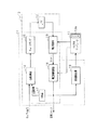
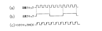
の電圧制御発振器16から出力される記録クロックは、PLL回路10内において分周器17により所定に分周され、その分周された信号が位相比較器14の他方の入力として帰還される。すなわち、PLL回路10は、このようなフィードバック動作を繰り返し行うことにより、電圧制御発振器16から出力される記録クロック、正確にはその分周信号をウォブル信号に同期させる。
その指令に基づいて上記同定した発振特性C1〜C9の中から「4倍速での書き込み指令」に適した発振特性を選択してこれを電圧制御発振器16に設定する。詳しくは、光ディスクの回転速度(4倍速)から想定されるウォブル信号の周波数が発振可能な周波数範囲内にあって且つ、その周波数範囲の略中心になるとともに、よりゲインの小さい発振特性を上記同定した発振特性C1〜C9の中から選択して電圧制御発振器16に設定する。上記クロック生成回路11では、こうして電圧制御発振器16に設定された発振特性にしたがって、ウォブル信号に同期した記録クロックを自動生成することとなる。
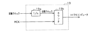
各別に備える構成としたが、1つの分周器を共用する構成としてもよい。例えば、分周器17を共用する場合、その分周器17により分周された後の分周信号をカウンタ19bの一方の入力とすることができる。
Claims (8)
- 印加される制御電圧に対し複数の異なる発振特性をもってクロック発振の可能な電圧制御発振器を用いて周期信号に同期したクロックを生成するクロック生成方法であって、
前記電圧制御発振器に設定されている発振特性を順次選択しつつ、同電圧制御発振器に試験電圧を与えて、それら発振特性の各々を同定し、該同定した各発振特性のうち、前記同期の対象とする周期信号の想定される周波数がそれら発振特性において発振可能な周波数範囲内にあって且つ、ゲインのより小さい発振特性を前記電圧制御発振器に設定して前記クロックの生成を行う
ことを特徴とするクロック生成方法。 - 前記順次選択される発振特性は、複数のオフセット周波数、及び電圧/周波数変換にかかる複数のゲインの組み合わせからなり、それら各発振特性に対する前記同定は、前記試験電圧として前記制御電圧がとりうる最大電圧及び最小電圧をそれぞれ前記電圧制御発振器に与えたときに同電圧制御発振器から出力されるクロックの周波数をそれぞれ検出し、これら検出される2つの周波数の値と前記与えた2つの電圧の値とから各々前記オフセット周波数及び前記ゲインを特定することによって行われる
請求項1に記載のクロック生成方法。 - 前記順次選択される発振特性は、複数のオフセット周波数、及び電圧/周波数変換にかかる複数のゲインの組み合わせからなり、それら各発振特性に対する前記同定は、前記試験電圧として前記制御電圧がとりうる最大電圧及び最小電圧の中間電圧を前記電圧制御発振器に与えたときに同電圧制御発振器から出力されるクロックの周波数を検出し、該検出される周波数の値と前記与えた電圧の値とから各々前記オフセット周波数及び前記ゲインを推定することによって行われる
請求項1に記載のクロック生成方法。 - 周期信号を入力し、この周期信号に同期したクロックを生成するクロック生成装置であって、
印加される制御電圧に対し複数の異なる発振特性をもってクロック発振の可能な電圧制御発振器と、この電圧制御発振器に設定されている発振特性の順次の選択に伴って同電圧制御発振器に試験電圧を与える電圧制御器と、前記試験電圧の付与によって前記電圧制御発振器から出力されるクロックの周波数を検出する周波数検出器とを備える
ことを特徴とするクロック生成装置。 - 請求項4に記載のクロック生成装置において、
前記電圧制御発振器に設定されている発振特性の順次選択に伴い前記電圧制御器から前記電圧制御発振器に付与される試験電圧の値とこの試験電圧に対応して前記周波数検出器によって検出される周波数の値とに基づいて前記電圧制御発振器に設定されている発振特性の各々が同定されるとともに、該同定された各発振特性のうち、前記同期の対象とする周期信号の想定される周波数がそれら発振特性において発振可能な周波数範囲内にあって且つ、ゲインのより小さい発振特性が、前記周期信号に同期したクロックを生成するための発振特性として前記電圧制御発振器に選択的に設定される
ことを特徴とするクロック生成装置。 - 前記順次選択される発振特性は、複数のオフセット周波数、及び電圧/周波数変換にかかる複数のゲインの組み合わせからなり、それら各発振特性に対する前記同定は、前記試験電圧として前記制御電圧がとりうる最大電圧及び最小電圧がそれぞれ電圧制御発振器に与えられて且つ、同電圧制御発振器から出力されるクロックの周波数が前記周波数検出器によってそれぞれ検出されたときの、これら検出される2つの周波数の値と前記与えられる2つの電圧の値とから各々前記オフセット周波数及び前記ゲインが特定されることによって行われる
請求項5に記載のクロック生成装置。 - 前記順次選択される発振特性は、複数のオフセット周波数、及び電圧/周波数変換にかかる複数のゲインの組み合わせからなり、それら各発振特性に対する前記
同定は、前記試験電圧として前記制御電圧がとりうる最大電圧及び最小電圧の中間電圧が電圧制御発振器に与えられて且つ、同電圧制御発振器から出力されるクロックの周波数が前記周波数検出器によって検出されたときの、該検出される周波数の値と前記与えられる電圧の値とから各々前記オフセット周波数及び前記ゲインが推定されることによって行われる
請求項5に記載のクロック生成装置。 - 前記同期の対象とする周期信号が、光ディスクから抽出される周期信号の一つであり、前記発振特性の同定、及びこの同定に基づく前記電圧制御発振器に対する発振特性の選択的な設定が、前記光ディスクとの間でのデータの記録・再生を行う光ディスク装置の起動毎に実行される
請求項4〜7のいずれか一項に記載のクロック生成装置。
Priority Applications (5)
| Application Number | Priority Date | Filing Date | Title |
|---|---|---|---|
| JP2004022818A JP4260034B2 (ja) | 2004-01-30 | 2004-01-30 | クロック生成方法及びクロック生成装置 |
| CN2005100043737A CN1652466B (zh) | 2004-01-30 | 2005-01-17 | 时钟生成方法和时钟生成装置 |
| US11/044,736 US7141961B2 (en) | 2004-01-30 | 2005-01-27 | Method and device for generating clock signal |
| TW094102416A TWI267722B (en) | 2004-01-30 | 2005-01-27 | Clock generating method and clock generating apparatus |
| KR1020050007866A KR100767167B1 (ko) | 2004-01-30 | 2005-01-28 | 클럭 신호 생성 방법 |
Applications Claiming Priority (1)
| Application Number | Priority Date | Filing Date | Title |
|---|---|---|---|
| JP2004022818A JP4260034B2 (ja) | 2004-01-30 | 2004-01-30 | クロック生成方法及びクロック生成装置 |
Publications (2)
| Publication Number | Publication Date |
|---|---|
| JP2005217841A true JP2005217841A (ja) | 2005-08-11 |
| JP4260034B2 JP4260034B2 (ja) | 2009-04-30 |
Family
ID=34805680
Family Applications (1)
| Application Number | Title | Priority Date | Filing Date |
|---|---|---|---|
| JP2004022818A Expired - Fee Related JP4260034B2 (ja) | 2004-01-30 | 2004-01-30 | クロック生成方法及びクロック生成装置 |
Country Status (5)
| Country | Link |
|---|---|
| US (1) | US7141961B2 (ja) |
| JP (1) | JP4260034B2 (ja) |
| KR (1) | KR100767167B1 (ja) |
| CN (1) | CN1652466B (ja) |
| TW (1) | TWI267722B (ja) |
Families Citing this family (22)
| Publication number | Priority date | Publication date | Assignee | Title |
|---|---|---|---|---|
| JP4925630B2 (ja) * | 2005-09-06 | 2012-05-09 | 株式会社アドバンテスト | 試験装置および試験方法 |
| US20070266263A1 (en) * | 2006-05-11 | 2007-11-15 | Silicon Integrated Systems Corp. | Speed adjustment system and method for performing the same |
| KR101354836B1 (ko) * | 2006-08-25 | 2014-01-22 | 엘지전자 주식회사 | 주파수 위상동기장치 및 위상동기방법 |
| JP4538476B2 (ja) * | 2007-08-27 | 2010-09-08 | 独立行政法人理化学研究所 | 半導体構造の形成方法 |
| JP2009054782A (ja) * | 2007-08-27 | 2009-03-12 | Institute Of Physical & Chemical Research | 光半導体素子及びその製造方法 |
| JP2011130604A (ja) | 2009-12-18 | 2011-06-30 | Sanyo Electric Co Ltd | 充電回路、増幅回路 |
| US9083356B1 (en) | 2013-03-14 | 2015-07-14 | Gsi Technology, Inc. | Systems and methods of phase-locked loop involving closed-loop, continuous frequency range, auto calibration and/or other features |
| US10854284B1 (en) | 2016-12-06 | 2020-12-01 | Gsi Technology, Inc. | Computational memory cell and processing array device with ratioless write port |
| US10860320B1 (en) | 2016-12-06 | 2020-12-08 | Gsi Technology, Inc. | Orthogonal data transposition system and method during data transfers to/from a processing array |
| US10777262B1 (en) | 2016-12-06 | 2020-09-15 | Gsi Technology, Inc. | Read data processing circuits and methods associated memory cells |
| US10847213B1 (en) | 2016-12-06 | 2020-11-24 | Gsi Technology, Inc. | Write data processing circuits and methods associated with computational memory cells |
| US10725777B2 (en) | 2016-12-06 | 2020-07-28 | Gsi Technology, Inc. | Computational memory cell and processing array device using memory cells |
| US10770133B1 (en) | 2016-12-06 | 2020-09-08 | Gsi Technology, Inc. | Read and write data processing circuits and methods associated with computational memory cells that provides write inhibits and read bit line pre-charge inhibits |
| US10847212B1 (en) | 2016-12-06 | 2020-11-24 | Gsi Technology, Inc. | Read and write data processing circuits and methods associated with computational memory cells using two read multiplexers |
| US10891076B1 (en) | 2016-12-06 | 2021-01-12 | Gsi Technology, Inc. | Results processing circuits and methods associated with computational memory cells |
| US10998040B2 (en) | 2016-12-06 | 2021-05-04 | Gsi Technology, Inc. | Computational memory cell and processing array device using the memory cells for XOR and XNOR computations |
| US10943648B1 (en) | 2016-12-06 | 2021-03-09 | Gsi Technology, Inc. | Ultra low VDD memory cell with ratioless write port |
| US11227653B1 (en) | 2016-12-06 | 2022-01-18 | Gsi Technology, Inc. | Storage array circuits and methods for computational memory cells |
| JP6828484B2 (ja) * | 2017-02-08 | 2021-02-10 | 株式会社デンソー | レーダ用pll回路 |
| US10930341B1 (en) | 2019-06-18 | 2021-02-23 | Gsi Technology, Inc. | Processing array device that performs one cycle full adder operation and bit line read/write logic features |
| US10958272B2 (en) | 2019-06-18 | 2021-03-23 | Gsi Technology, Inc. | Computational memory cell and processing array device using complementary exclusive or memory cells |
| US10877731B1 (en) | 2019-06-18 | 2020-12-29 | Gsi Technology, Inc. | Processing array device that performs one cycle full adder operation and bit line read/write logic features |
Family Cites Families (6)
| Publication number | Priority date | Publication date | Assignee | Title |
|---|---|---|---|---|
| JP3208736B2 (ja) * | 1991-11-08 | 2001-09-17 | ソニー株式会社 | Pll回路 |
| JPH1131966A (ja) * | 1997-06-03 | 1999-02-02 | Motorola Inc | 電圧制御発振器に関する装置および同調方法 |
| JP2944607B2 (ja) * | 1998-02-12 | 1999-09-06 | 日本電気アイシーマイコンシステム株式会社 | ディジタルpll回路とクロックの生成方法 |
| JP2000278124A (ja) * | 1999-03-26 | 2000-10-06 | Sanyo Electric Co Ltd | Pll回路 |
| US6292507B1 (en) * | 1999-09-01 | 2001-09-18 | Lexmark International, Inc. | Method and apparatus for compensating a spread spectrum clock generator |
| JP2001076437A (ja) * | 1999-09-06 | 2001-03-23 | Victor Co Of Japan Ltd | クロック信号発生装置 |
-
2004
- 2004-01-30 JP JP2004022818A patent/JP4260034B2/ja not_active Expired - Fee Related
-
2005
- 2005-01-17 CN CN2005100043737A patent/CN1652466B/zh not_active Expired - Fee Related
- 2005-01-27 TW TW094102416A patent/TWI267722B/zh not_active IP Right Cessation
- 2005-01-27 US US11/044,736 patent/US7141961B2/en not_active Expired - Lifetime
- 2005-01-28 KR KR1020050007866A patent/KR100767167B1/ko not_active Expired - Fee Related
Also Published As
| Publication number | Publication date |
|---|---|
| KR100767167B1 (ko) | 2007-10-15 |
| JP4260034B2 (ja) | 2009-04-30 |
| TWI267722B (en) | 2006-12-01 |
| CN1652466A (zh) | 2005-08-10 |
| US7141961B2 (en) | 2006-11-28 |
| TW200528958A (en) | 2005-09-01 |
| US20050168253A1 (en) | 2005-08-04 |
| KR20050078223A (ko) | 2005-08-04 |
| CN1652466B (zh) | 2010-04-28 |
Similar Documents
| Publication | Publication Date | Title |
|---|---|---|
| JP4260034B2 (ja) | クロック生成方法及びクロック生成装置 | |
| JP3910986B2 (ja) | 光ディスク装置 | |
| JPH1173645A (ja) | 光ディスク装置 | |
| US7065017B2 (en) | Optical disk apparatus, method for generating clock signal of optical disk apparatus, and method for setting amount of light of optical disk apparatus | |
| US7304523B2 (en) | Clock generating apparatus and method in optical storage system | |
| JP2004159161A (ja) | 遅延信号生成装置及び記録パルス生成装置 | |
| JP3820856B2 (ja) | 光ディスク記録装置 | |
| CN100452181C (zh) | Pll时钟发生器及其控制方法和光盘装置 | |
| CN101547006B (zh) | 相位同步电路 | |
| KR100585899B1 (ko) | Pll 회로 | |
| US6914465B2 (en) | Voltage-controlled osillator | |
| US6992958B2 (en) | Phase-locked loop circuit for reproducing a channel clock | |
| JP2002230752A (ja) | ウォブル欠陥検出装置及び方法 | |
| JP3649955B2 (ja) | データ記録用クロック信号発生装置 | |
| US7038987B2 (en) | Optical disk device | |
| KR100213261B1 (ko) | 위상동기루프의 주파수검출기 | |
| JP2004253057A (ja) | クロック生成装置 | |
| JP2001357620A (ja) | 光ディスク記録装置とその半導体集積回路 | |
| JP2005510001A (ja) | ウォブル信号から信号を生成する手段を備える、情報を記録または再生する装置 | |
| JP4494941B2 (ja) | データ記録用クロック信号発生回路 | |
| JP2004178655A (ja) | クロック生成回路及びそれを用いた記録再生装置 | |
| US20070205737A1 (en) | Control circuit and method of controlling rotation frequency of spindle in optical disc drive for reducing frequency difference of output signals respectively corresponding to different disc rotation modes | |
| JP2004343724A (ja) | Pllクロック発生器、光ディスク装置およびpllクロック発生器の制御方法 | |
| JP2005071606A (ja) | データ記録用クロック信号発生装置 | |
| JP2002230757A (ja) | クロック生成回路及びそれを用いた記録再生装置 |
Legal Events
| Date | Code | Title | Description |
|---|---|---|---|
| RD01 | Notification of change of attorney |
Free format text: JAPANESE INTERMEDIATE CODE: A7421 Effective date: 20051227 |
|
| A621 | Written request for application examination |
Free format text: JAPANESE INTERMEDIATE CODE: A621 Effective date: 20070112 |
|
| A977 | Report on retrieval |
Free format text: JAPANESE INTERMEDIATE CODE: A971007 Effective date: 20081003 |
|
| A131 | Notification of reasons for refusal |
Free format text: JAPANESE INTERMEDIATE CODE: A131 Effective date: 20081014 |
|
| A521 | Request for written amendment filed |
Free format text: JAPANESE INTERMEDIATE CODE: A523 Effective date: 20081204 |
|
| TRDD | Decision of grant or rejection written | ||
| A01 | Written decision to grant a patent or to grant a registration (utility model) |
Free format text: JAPANESE INTERMEDIATE CODE: A01 Effective date: 20090106 |
|
| A01 | Written decision to grant a patent or to grant a registration (utility model) |
Free format text: JAPANESE INTERMEDIATE CODE: A01 |
|
| A61 | First payment of annual fees (during grant procedure) |
Free format text: JAPANESE INTERMEDIATE CODE: A61 Effective date: 20090203 |
|
| FPAY | Renewal fee payment (event date is renewal date of database) |
Free format text: PAYMENT UNTIL: 20120220 Year of fee payment: 3 |
|
| R151 | Written notification of patent or utility model registration |
Ref document number: 4260034 Country of ref document: JP Free format text: JAPANESE INTERMEDIATE CODE: R151 |
|
| FPAY | Renewal fee payment (event date is renewal date of database) |
Free format text: PAYMENT UNTIL: 20120220 Year of fee payment: 3 |
|
| FPAY | Renewal fee payment (event date is renewal date of database) |
Free format text: PAYMENT UNTIL: 20130220 Year of fee payment: 4 |
|
| R250 | Receipt of annual fees |
Free format text: JAPANESE INTERMEDIATE CODE: R250 |
|
| FPAY | Renewal fee payment (event date is renewal date of database) |
Free format text: PAYMENT UNTIL: 20140220 Year of fee payment: 5 |
|
| R250 | Receipt of annual fees |
Free format text: JAPANESE INTERMEDIATE CODE: R250 |
|
| R250 | Receipt of annual fees |
Free format text: JAPANESE INTERMEDIATE CODE: R250 |
|
| R250 | Receipt of annual fees |
Free format text: JAPANESE INTERMEDIATE CODE: R250 |
|
| R250 | Receipt of annual fees |
Free format text: JAPANESE INTERMEDIATE CODE: R250 |
|
| R250 | Receipt of annual fees |
Free format text: JAPANESE INTERMEDIATE CODE: R250 |
|
| R250 | Receipt of annual fees |
Free format text: JAPANESE INTERMEDIATE CODE: R250 |
|
| R250 | Receipt of annual fees |
Free format text: JAPANESE INTERMEDIATE CODE: R250 |
|
| R250 | Receipt of annual fees |
Free format text: JAPANESE INTERMEDIATE CODE: R250 |
|
| R250 | Receipt of annual fees |
Free format text: JAPANESE INTERMEDIATE CODE: R250 |
|
| LAPS | Cancellation because of no payment of annual fees |