US10847213B1 - Write data processing circuits and methods associated with computational memory cells - Google Patents
Write data processing circuits and methods associated with computational memory cells Download PDFInfo
- Publication number
- US10847213B1 US10847213B1 US16/111,183 US201816111183A US10847213B1 US 10847213 B1 US10847213 B1 US 10847213B1 US 201816111183 A US201816111183 A US 201816111183A US 10847213 B1 US10847213 B1 US 10847213B1
- Authority
- US
- United States
- Prior art keywords
- bit line
- read
- line section
- section
- array
- Prior art date
- Legal status (The legal status is an assumption and is not a legal conclusion. Google has not performed a legal analysis and makes no representation as to the accuracy of the status listed.)
- Active
Links
- 238000012545 processing Methods 0.000 title claims abstract description 71
- 238000000034 method Methods 0.000 title abstract description 14
- 238000013500 data storage Methods 0.000 description 29
- 230000006870 function Effects 0.000 description 23
- 230000009977 dual effect Effects 0.000 description 22
- 239000004065 semiconductor Substances 0.000 description 12
- 230000000295 complement effect Effects 0.000 description 9
- 238000005516 engineering process Methods 0.000 description 5
- 238000004891 communication Methods 0.000 description 4
- 230000007246 mechanism Effects 0.000 description 4
- 230000004048 modification Effects 0.000 description 4
- 238000012986 modification Methods 0.000 description 4
- 230000003068 static effect Effects 0.000 description 4
- 239000013598 vector Substances 0.000 description 4
- 238000002955 isolation Methods 0.000 description 3
- 230000008569 process Effects 0.000 description 3
- 238000003491 array Methods 0.000 description 2
- 238000007599 discharging Methods 0.000 description 2
- 239000002184 metal Substances 0.000 description 2
- 229910044991 metal oxide Inorganic materials 0.000 description 2
- 150000004706 metal oxides Chemical class 0.000 description 2
- 230000003287 optical effect Effects 0.000 description 2
- XUIMIQQOPSSXEZ-UHFFFAOYSA-N Silicon Chemical compound [Si] XUIMIQQOPSSXEZ-UHFFFAOYSA-N 0.000 description 1
- 230000003542 behavioural effect Effects 0.000 description 1
- 230000008901 benefit Effects 0.000 description 1
- 230000005540 biological transmission Effects 0.000 description 1
- 229920000547 conjugated polymer Polymers 0.000 description 1
- 238000011982 device technology Methods 0.000 description 1
- 230000005669 field effect Effects 0.000 description 1
- 230000008676 import Effects 0.000 description 1
- 230000005055 memory storage Effects 0.000 description 1
- 230000001537 neural effect Effects 0.000 description 1
- 229920000642 polymer Polymers 0.000 description 1
- 238000004549 pulsed laser deposition Methods 0.000 description 1
- 229910052710 silicon Inorganic materials 0.000 description 1
- 239000010703 silicon Substances 0.000 description 1
- 238000012546 transfer Methods 0.000 description 1
Images


Classifications
-
- H—ELECTRICITY
- H03—ELECTRONIC CIRCUITRY
- H03K—PULSE TECHNIQUE
- H03K19/00—Logic circuits, i.e. having at least two inputs acting on one output; Inverting circuits
- H03K19/02—Logic circuits, i.e. having at least two inputs acting on one output; Inverting circuits using specified components
- H03K19/08—Logic circuits, i.e. having at least two inputs acting on one output; Inverting circuits using specified components using semiconductor devices
- H03K19/094—Logic circuits, i.e. having at least two inputs acting on one output; Inverting circuits using specified components using semiconductor devices using field-effect transistors
- H03K19/0944—Logic circuits, i.e. having at least two inputs acting on one output; Inverting circuits using specified components using semiconductor devices using field-effect transistors using MOSFET or insulated gate field-effect transistors, i.e. IGFET
-
- G—PHYSICS
- G11—INFORMATION STORAGE
- G11C—STATIC STORES
- G11C11/00—Digital stores characterised by the use of particular electric or magnetic storage elements; Storage elements therefor
- G11C11/21—Digital stores characterised by the use of particular electric or magnetic storage elements; Storage elements therefor using electric elements
- G11C11/34—Digital stores characterised by the use of particular electric or magnetic storage elements; Storage elements therefor using electric elements using semiconductor devices
- G11C11/40—Digital stores characterised by the use of particular electric or magnetic storage elements; Storage elements therefor using electric elements using semiconductor devices using transistors
- G11C11/41—Digital stores characterised by the use of particular electric or magnetic storage elements; Storage elements therefor using electric elements using semiconductor devices using transistors forming static cells with positive feedback, i.e. cells not needing refreshing or charge regeneration, e.g. bistable multivibrator or Schmitt trigger
- G11C11/413—Auxiliary circuits, e.g. for addressing, decoding, driving, writing, sensing, timing or power reduction
- G11C11/417—Auxiliary circuits, e.g. for addressing, decoding, driving, writing, sensing, timing or power reduction for memory cells of the field-effect type
- G11C11/418—Address circuits
-
- G—PHYSICS
- G11—INFORMATION STORAGE
- G11C—STATIC STORES
- G11C11/00—Digital stores characterised by the use of particular electric or magnetic storage elements; Storage elements therefor
- G11C11/21—Digital stores characterised by the use of particular electric or magnetic storage elements; Storage elements therefor using electric elements
- G11C11/34—Digital stores characterised by the use of particular electric or magnetic storage elements; Storage elements therefor using electric elements using semiconductor devices
- G11C11/40—Digital stores characterised by the use of particular electric or magnetic storage elements; Storage elements therefor using electric elements using semiconductor devices using transistors
- G11C11/41—Digital stores characterised by the use of particular electric or magnetic storage elements; Storage elements therefor using electric elements using semiconductor devices using transistors forming static cells with positive feedback, i.e. cells not needing refreshing or charge regeneration, e.g. bistable multivibrator or Schmitt trigger
- G11C11/413—Auxiliary circuits, e.g. for addressing, decoding, driving, writing, sensing, timing or power reduction
- G11C11/417—Auxiliary circuits, e.g. for addressing, decoding, driving, writing, sensing, timing or power reduction for memory cells of the field-effect type
- G11C11/419—Read-write [R-W] circuits
-
- G—PHYSICS
- G11—INFORMATION STORAGE
- G11C—STATIC STORES
- G11C7/00—Arrangements for writing information into, or reading information out from, a digital store
- G11C7/10—Input/output [I/O] data interface arrangements, e.g. I/O data control circuits, I/O data buffers
- G11C7/1006—Data managing, e.g. manipulating data before writing or reading out, data bus switches or control circuits therefor
-
- G—PHYSICS
- G11—INFORMATION STORAGE
- G11C—STATIC STORES
- G11C7/00—Arrangements for writing information into, or reading information out from, a digital store
- G11C7/10—Input/output [I/O] data interface arrangements, e.g. I/O data control circuits, I/O data buffers
- G11C7/1015—Read-write modes for single port memories, i.e. having either a random port or a serial port
- G11C7/1036—Read-write modes for single port memories, i.e. having either a random port or a serial port using data shift registers
-
- G—PHYSICS
- G11—INFORMATION STORAGE
- G11C—STATIC STORES
- G11C7/00—Arrangements for writing information into, or reading information out from, a digital store
- G11C7/10—Input/output [I/O] data interface arrangements, e.g. I/O data control circuits, I/O data buffers
- G11C7/1075—Input/output [I/O] data interface arrangements, e.g. I/O data control circuits, I/O data buffers for multiport memories each having random access ports and serial ports, e.g. video RAM
Definitions
- the disclosure relates generally to a computational memory element and in particular to a computational memory element having write data processing.
- Memory cells have traditionally been used to store bits of data. It is also possible to architect a memory cell so that the memory cell is able to perform some simple logical functions when multiple memory cells are connected to the same read bit line. For example, when memory cells A, B, and C are connected to a particular read bit line and are read simultaneously, and the memory cells and read bit line circuitry are designed to produce a logical AND result, then the result that appears on the read bit line is AND(a,b,c) (i.e. “a AND b AND c”), where a, b, and c represent the binary data values stored in memory cells A, B, and C respectively.
- these computational memory cells and read bit line circuitry allow for a single logical function (e.g. AND) to be performed across multiple memory cells connected to the same read bit line, when read simultaneously.
- a single logical function e.g. AND
- more complex logical functions across multiple memory cells connected to the same read bit line are desirable.
- FIG. 1 illustrates an example of a semiconductor memory that may include a plurality of computation memory cells and write circuitry
- FIG. 2 illustrates an example of a computer system that may include a plurality of computation memory cells and a write circuitry
- FIG. 3A illustrates an example of a processing array with computational memory cells that may be incorporated into a semiconductor memory or computer system
- FIG. 3B illustrates the processing array with computational memory cells having one section and multiple bit line sections
- FIG. 3C illustrates the processing array with computational memory cells having multiple sections and multiple bit line sections
- FIGS. 4A and 4B illustrate examples of two different types of computational memory cells that may be used in the semiconductor memory of FIG. 1 , the computer system of FIG. 2 or the processing array of FIGS. 3A-3C ;
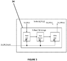
- FIG. 5 illustrates read/write logic including read logic, read data storage, and write logic associated with each bit line section in the processing array device depicted in FIG. 3C ;
- FIG. 6 illustrates a processing array device comprising “k” sections with “n” bit lines in each section, where each bit line within each section connects to “m” computational memory cells;
- FIG. 7 illustrates the read logic, read data storage, and write logic associated with each bit line section in the processing array device depicted in FIG. 6 ;
- FIG. 8 illustrates the read logic, read data storage, and write logic associated with each bit line section in the processing array device depicted in FIG. 6 with the ability to invert the selected data before it is stored in the bit line section.
- the disclosure is particularly applicable to a processing array, semiconductor memory or computer that utilizes a plurality of computational memory cells (with each cell being formed with a static random access memory (SRAM) cell) and additional write processing circuitry to provide more complex logical functions based on the data read out of the computational memory cells and it is in this context that the disclosure will be described.
- each memory cell may be other types of volatile and non-volatile memory cell that are within the scope of the disclosure, that other additional write circuitry (including more, less or different logic) may be used are within the scope of the disclosure or that different computational memory cell architectures that those disclosed below are within the scope of the disclosure.
- the disclosure is directed to a memory/processing array that has a plurality of computing memory cells in an array with additional write processing circuitry.
- a column of computing memory cells in the array may each have a read bit line and the read bit line for each of the computing memory cells in the column may be tied together as a single read bit line.
- the memory/processing array may be subdivided into one or more sections (an example of which is shown in FIGS. 3B and 3C ) wherein each section has a unique set of “n” bit lines (each bit line being part of a bit line section) where each bit line section comprises a single read bit line and a pair of positive and negative write bit lines, with each bit line connected to “m” computational memory cells.
- Each bit line section also may have a read data storage that is used to capture and store the read result from the read bit line during read operations (so a read data storage is implemented per read bit line) and write circuitry for shifting read data among the bit line sections of the array.
- BL-Sect[x,y] is a shorthand notation indicating a bit line section with bit line “y” in section “x”.
- Write circuitry is disclosed that may be used with the memory/processing array with the sections above since it is desirable to be able to shift data between adjacent bit lines in the same section (e.g. between bl-sect[x,y] and bl-sect[x,y+1]), and between the same relative bit lines in adjacent sections (e.g. between bl-sect[x,y] and bl-sect[x+1,y]).
- each bit line section (such as bl-sect[x,y]) is connected not only to that bl-sect's write circuitry, but also to the write circuitry associated with its horizontally and vertically adjacent neighbor bl-sects: for example, bl-sect[x,y ⁇ 1], bl-sect[x,y+1], bl-sect[x ⁇ 1,y], and bl-sect[x+1,y] for a bit line section in the middle of the array with bit line yin section x.
- the write circuitry in each bl-sect[x,y] receives the read data storage outputs from 5 bl-sects—itself and its 4 neighbors, and during write operations a 5:1 mux is used to select one of those 5 read data storage outputs as the write data for that bit line section (“bl-sect”). It is also desirable to be able to invert the selected data (i.e. the 5:1 mux output) before it is stored in the bl-sect during a write operation.
- the write processing circuitry may have some simple logic along with a write data inversion control signal to facilitate the write data inversion.
- FIG. 1 illustrates an example of a semiconductor memory 10 that may include a plurality of computation memory cells and write circuitry that are described below in more detail.
- the below disclosed plurality of computation memory cells and write circuitry allow the semiconductor memory 10 to perform more complex logic functions than are possible with just the plurality of computation memory cells.
- FIG. 2 illustrates an example of a computer system 20 that may include a plurality of computation memory cells and write circuitry that are described below in more detail.
- the below disclosed plurality of computation memory cells and write circuitry allow the semiconductor memory 20 to perform more complex logic functions than are possible with just the plurality of computation memory cells.
- the computer system 20 may have at least one processor 22 and a memory 24 that may include the plurality of computation memory cells and write circuitry.
- FIG. 3A illustrates an example of a processing array 30 with computational memory cells in an array that may be incorporated into a semiconductor memory or computer system.
- the processing array 30 may include an array of computational memory cells (cell 00, . . . , cell 0n and cell m0, . . . , cell mn).
- the array of computational memory cells may be rectangular as shown in FIG. 3 and may have a plurality of columns and a plurality of rows wherein the computational memory cells in a particular column may also be connected to the same read bit line (RBL).
- RBL read bit line
- the processing array 30 may further include a wordline (WL) generator and read/write logic control circuit 32 that may be connected to and generate signals for the read word line (RE) and write word line (WE) for each memory cell (such as R 0 , . . . , REn and WE 0 , . . . , WEn) to control the read and write operations as well known and one more read/write blocks 34 that are connected to the read and write bit lines of the computational memory cells.
- the processing array may have read/write circuitry 34 for each set of bit line signals of the computational memory cells.
- BL 0 read/write logic 340 may be coupled to the read and write bit lines (WBLb 0 , WBL 0 and RBL 0 ) for the computational memory cells in column 0 of the array and BLn read/write logic 34 n may be coupled to the read and write bit lines (WBLbn, WBLn and RBLn) for the computational memory cells in column n of the array as shown in FIG. 3 .
- the wordline (WL) generator and read/write logic control circuit 32 may also generate one or more control signals that control the read/write circuitry 34 .
- the one or more control signals may include a Read_Done control signal, an XORacc_En control signal, an ANDacc_En control signal and an ORacc_En control signal.
- control signals are used so that the wordline (WL) generator and read/write logic control circuit 32 may generate different control signals for each embodiment or the wordline (WL) generator and read/write logic control circuit 32 may generate each of the control signals, but then only certain of the control signals or all of the control signals may be utilized as described in the above incorporated by reference co-pending patent application.
- the wordline (WL) generator and read/write logic control circuit 32 may activate one or more word lines that activate one or more computational memory cells so that the read bit lines of those one or more computational memory cells may be read out. Further details of the read operation are not provided here since the read operation is well known.
- FIGS. 3B and 3C illustrate the processing array 30 with computational memory cells having sections having the same elements as shown in FIG. 3A .
- the array 30 in FIG. 3B has one section (Section 0) with “n” bit lines (bit line 0 (BL 0 ), . . . , bit line n (BLn)) in different bit line sections, where each bit line connects to “m” computational memory cells (cell 00, . . . , cell m0 for bit line 0 for example).
- the m cells may be the plurality of computational memory cells that are part of each column of the array 30 .
- FIG. 3C illustrates the processing array 30 with computational memory cells having multiple sections. In the example in FIG.
- the processing array device 30 comprises “k” sections with “n” bit lines each, where each bit line within each section connects to “m” computational memory cells. Note that the other elements of the processing array 30 are present in FIG. 3C , but not shown for clarity. In FIG. 3C , there are no read data storageoutput paths between horizontally adjacent bit lines in the same section, nor between the same relative bit line in vertically adjacent sections.
- the BL-Sect(0,0) block shown corresponds to the BL-Sect(0,0) shown in FIG. 3B with the plurality of computational memory cells and the read/write logic 340 and each other block shown in FIG. 3C corresponds to a separate portion of the processing array. As shown in FIG.
- the set of control signals, generated by the wordline generator and read/write logic controller 32 , for each section may include one or more read enable control signals (for example S[0]_RE[m:0] for section 0), one or more write enable control signals (for example S[0]_WE[m:0] for section 0) and one or more read/write control signals (for example S[0]_RW_Ctrl[p:0] for section 0).
- read enable control signals for example S[0]_RE[m:0] for section 0
- write enable control signals for example S[0]_WE[m:0] for section 0
- read/write control signals for example S[0]_RW_Ctrl[p:0] for section 0
- FIGS. 4A and 4B illustrate examples of two different types of computational memory cells that may be used in the semiconductor memory of FIG. 1 , the computer system of FIG. 2 or the processing array of FIGS. 3 and 6 .
- the computational memory cell are based on an SRAM memory cell.
- FIG. 4A illustrates an example of a dual port SRAM cell 20 that may be used for computation.
- the dual port SRAM cell may include two cross coupled inverters 121 , 122 and two access transistors M 23 and M 24 that interconnected together to form a 6T SRAM cell.
- the SRAM may be operated as storage latch and may have a write port.
- the two inverters are cross coupled since the input of the first inverter is connected to the output of the second inverter and the output of the first inverter is coupled to the input of the second inverter as shown in FIG. 4A .
- a Write Word line carries a signal and is called WE and a write bit line and its complement are called WBL and WBLb, respectively.
- the Write word line WE is coupled to the gates of the two access transistors M 23 , M 24 that are part of the SRAM cell.
- the write bit line and its complement (WBL and WBLb) are each coupled to one side of the respective access transistors M 23 , M 24 as shown in FIG. 4A while the other side of each of those access transistors M 23 , M 24 are coupled to each side of the cross coupled inverters (labeled D and Db in FIG. 4A .)
- the circuit in FIG. 4A may also have a read word line RE, a read bit line RBL and a read port formed by transistors M 21 , M 22 coupled together to form as isolation circuit as shown.
- the read word line RE may be coupled to the gate of transistor M 21 that forms part of the read port while the read bit line is coupled to the source terminal of transistor M 21 .
- the gate of transistor M 22 may be coupled to the Db output from the cross coupled inverters 121 , 122 .
- multiple cells can turn on to perform an AND function.
- RBL is pre-charged high and if the Db signal of all cells that are turned on by RE is “0”, then RBL stays high since, although the gate of transistor M 21 is turned on by the RE signal, the gate of M 22 is not turned on and the RBL line is not connected to the ground to which the drain of transistor M 22 is connected. If the Db signal of any or all of the cells is “1” then RBL is discharged to 0 since the gate of M 22 is turned on and the RBL line is connected to ground.
- RBL NOR (Db 0 , Db 1 , etc.) where Db 0 , Db 1 , etc. are the complementary data of the SRAM cells that have been turned on by the RE signal.
- the Db signal of the cell 20 may be coupled to a gate of transistor M 22 to drive the RBL.
- the Db signal is isolated from the RBL line and its signal/voltage level by the transistors M 21 , M 22 . Because the Db signal/value is isolated from the RBL line and signal/voltage level, the Db signal is not susceptive to the lower bit line level caused by multiple “0” data stored in multiple cells in contrast to the typical SRAM cell. Therefore, for the cell in FIG. 4A , there is no limitation of how many cells can be turned on to drive RBL.
- the cell offers more operands for the AND function since there is no limit of how many cells can be turned on to drive RBL.
- the RBL line is pre-charged (not a static pull up transistor as with the typical 6T cell) so this cell can provide much faster sensing because the current generated by the cell is all be used to discharge the bit line capacitance with no current being consumed by a static pull up transistor so that the bit line discharging rate can be faster by more than 2 times.
- the sensing for the disclosed cell is also lower power without the extra current consumed by a static pull up transistor and the discharging current is reduced by more than half.
- the write port of the cell in FIG. 4A is operated in the same manner as the 6T typical SRAM cell.
- the write cycle and Selective Write cycle for the cell have the same limitation as the typical 6T cell.
- FIG. 4B illustrates an implementation of a dual port SRAM cell 100 with an XOR function.
- the dual port SRAM cell 100 may include two cross coupled inverters 131 , 132 and two access transistors M 33 and M 34 that are interconnected together as shown in FIG. 4B to form the basic SRAM cell.
- the SRAM may be operated as storage latch and may have a write port.
- the two inverters 131 , 132 are cross coupled since the input of the first inverter is connected to the output of the second inverter (labeled D) and the output of the first inverter (labeled Db) is coupled to the input of the second inverter as shown in FIG. 4B .
- the cross coupled inverters 131 , 132 form the latch of the SRAM cell.
- the access transistor M 33 and M 34 may have their respective gates connected to write bit line and its complement (WBL, WBLb) respectively.
- a Write Word line carries a signal WE.
- the Write word line WE is coupled to the gate of a transistor M 35 that is part of the access circuitry for the SRAM cell.
- the circuit in FIG. 4B may also have a read word line RE, a read bit line RBL and a read port formed by transistors M 31 , M 32 coupled together to form as isolation circuit as shown.
- the read word line RE may be coupled to the gate of transistor M 31 that forms part of the read port while the read bit line RBL is coupled to the drain terminal of transistor M 31 .
- the gate of transistor M 32 may be coupled to the Db output from the cross coupled inverters 131 , 132 .
- the isolation circuit isolates the latch output Db (in the example in FIG. 4B ) from the read bit line and signal/voltage level so that the Db signal is not susceptive to the lower bit line level caused by multiple “0” data stored in multiple cells in contrast to the typical SRAM cell.
- the cell 100 may further include two more read word line transistors M 36 , M 37 and one extra complementary read word line, REb.
- REb When the read port is active, either RE or REb is high and the REb signal/voltage level is the complement of RE signal/voltage level.
- RBL is pre-charged high, and if one of (M 31 , M 32 ) or (M 36 , M 37 ) series transistors is on, RBL is discharged to 0. If none of (M 31 , M 32 ) or (M 36 , M 37 ) series transistors is on, then RBL stay high as 1 since it was precharged high.
- the word size is 8, then it needs to be stored in 8 cells (with one cell being shown in FIG. 4B ) on the same bit line.
- RBL AND(XNOR(RE1,D1),XNOR(RE2,D2), . . . ,XNOR(RE i ,D i )), where i is the number of active cell. (EQ2)
- D 1 , D 2 , . . . Dn are “n” number of data with RE on and Dbn+1, Dbn+2, . . . Dbm are m-n number of data with REb on.
- D 1 , D 2 , . . . Dn are n number of data with RE on and Dbn+1, Dbn+2, . . . Dbm are m ⁇ n number of data with REb on.
- the read port of the circuit 100 is FIG. 4B may be reconfigured differently to achieve different Boolean equation.
- transistors M 31 , M 32 , M 36 and M 37 may be changed to PMOS and the source of M 32 and M 37 is VDD instead of VSS, the bit line is pre-charged to 0 instead of 1 and the word line RE active state is 0.
- the logic equations EQ1 is inverted so that RBL is an XOR function of RE and D (EQ6).
- D 1 , D 2 , . . . Dn are n number of data with RE on and Dbn+1, Dbn+2, . . . Dbm are m ⁇ n number of data with REb on.
- RBL XNOR(RE,D) (EQ8)
- RBL NAND(D1,D2, . . . ,D n ,Db n +1,Db n +2, . . . Db m ) (EQ9)
- D 1 , D 2 , . . . Dn are n number of data with RE on and Dbn+1, Dbn+2, . . . Dbm are m ⁇ n number of data with REb on.
- FIG. 5 illustrates the read/write circuitry 34 including read logic, read data storage, and write logic associated with each bl-sect in the processing array device depicted in FIG. 3C .
- the read/write circuitry 34 for each section may include read circuitry 50 , a read storage 52 , implemented as a register, and write circuitry 54 .
- the read circuitry 50 and read storage 52 allows the data on the read bit lines connected to the particular read circuitry and read storage to accumulate so that more complex Boolean logic operations may be performed.
- Various implementations of the read circuitry 50 and read storage 52 may be found in Ser. No. 16/111,178, filed Aug. 23, 2018 that is co-pending and co-owned and is incorporated herein by reference.
- the write circuitry 54 manages the writing of data from each section.
- Each of the read circuitry 50 , read storage 52 and write circuitry 54 may be connected to one or more control signals (S[x]_RW_Ctrl[p:0] in the example implementation shown in FIG. 5 ) that control the operation of each of the circuits.
- the control signals may include the read control signals that are described above in the incorporated by reference patent application.
- the read circuitry 50 may receive inputs from the read bit lines of the computing memory cells of the section (S[x]_RBL[y]) and the write circuitry 54 may receive an input from the read data storage 52 and output data to the word bit lines of the computing memory cells of the section (S[x]_WBL[y] and S[x]_WBLb[y] in the example in FIG. 5 ).
- the read storage 52 output is only connected to the write circuitry 54 associated with its own bl-sect. Consequently, the write circuitry 54 associated with each bl-sect receives the read data storageoutput only from its own bl-sect, and therefore each bl-sect can only store/write data from its own read data storage.
- the processing array may place 1 bit (the same relative bit) from each vector in a single bl-sect so that the entire vectors are spread over 16 bl-sects (say, the same relative bit line across multiple sections).
- One way to perform the addition in this case is to add the first least significant bits (LSBs) of the 2 vectors (say in bl-sect[0,0]) to generate a “sum” bit and a “carry” bit.
- the carry bit then needs to be shifted to the bl-sect that contains the next (2 nd ) 2 LSBs (say bl-sect[1,0]), so that those 2 LSBs plus the carry bit can then be added together to generate the next sum and carry bits. That next (2 nd ) carry bit then needs to be shifted to the bl-sect that contains the next (3 rd ) 2 LSBs (bl-sect[2,0]). Etc. So the shifting ability described here provides a mechanism to shift carry bits during an “add” computaion.
- One way to provide a mechanism to shift data between adjacent bit lines in the same section, and between the same relative bit lines in adjacent sections, is to connect the read storage 52 output in each bl-sect[x,y] not only to that bl-sect's write logic 54 , but also to the write logic 54 associated with its 4 horizontally and vertically adjacent neighbor bl-sects: bl-sect[x,y ⁇ 1], bl-sect[x,y+1], bl-sect[x ⁇ 1,y], and bl-sect[x+1,y]. Consequently, the write logic 54 for a particular bl-sect receives the read data storage 52 outputs from 5 bl-sects—itself plus its 4 horizontally and vertically adjacent neighbors.
- a 5:1 write mux (shown in FIGS. 7-8 and described below) in some embodiments may be used to select which of those 5 read data storage outputs is used as the write data source to the bl-sect during a write operation.
- the one or more control signals shown in FIG. 5 from the WL generator and read/write logic controller and described above may include S[x]_wmux_sel[2:0] control signals for each section that are used to control the write mux selection during the write operation for each section.
- each bl-sect can store the read data storage output data (as produced by one or more read operations) from any of the 5 bl-sects—itself plus its 4 neighbors as described, thereby providing a mechanism to shift data between horizontally and vertically adjacent bl-sects.
- FIG. 6 illustrates a processing array device 30 consisting of “k” sections (Section 0, . . . , Section k in the example in FIG. 6 ) with “n” bit lines per section and thus shows a 2-dimensional “k by n” array of bl-sects.
- each bl-sect has 5 read data storage outputs (its own read data storage output plus the read data storage outputs from its 4 neighbor bl-sects) feeding the write logic of the bl-sect so that the write logic receives as input each of the read data storage output signals.
- each section includes one or more bit line sections (Sect-BL 0 , . . . , Sect-BLn) in a row of the processing array.
- the “k by n” exemplary array of bl-sects in FIG. 6 has four “edges” including two horizontal edges and two vertical edges.
- the bl-sects 600 along the two horizontal edges of the “k by n” array are BL-Sect[0,0], . . . , BL-Sect[0,n] and BL-Sect[k,0], . . . , BL-Sect[k:n] with the BL-Sect[0,0], . . . , BL-Sect[0,n] contained in the dashed line boxes in FIG. 6 .
- the bl-sects 602 along the two vertical edges of the “k by n” array are BL-Sect[0,0], . . . BL-Sect[k,0] & BL-Sect[0,n], . . . BL-Sect[k,n] with the BL-Sect[0,n], . . . BL-Sect[k,n] contained in a dashed line box.
- the “k by n” array of bl-sects in FIG. 6 has four “corners” at the intersection of each pair of “edges”.
- the subset of 4 “corner” bl-sects within the set of “edge” bl-sects in the “k by n” array are BL-Sect[0,0], BL-Sect[0,n], BL-Sect[k,0], & BL-Sect[k,n] in the example in FIG. 6 .
- the horizontal and vertical edge bl-sects (excluding the subset of “corner” bl-sects) lack one adjacent neighbor bl-sect whose location depends on the particular “edge” bl-sect.
- the “corner” bl-sects lack two adjacent neighbor bl-sects whose location depends on the particular “corner” bl-sect.
- the two neighbor bl-sects may include an adjacent bit line section (such as BL-Sect[0,1] for the corner bl-sect BL-Sect[0,0]) having an adjacent single read bit line (bit line 1 in section 0 for example) horizontally adjacent to the corner bit line section and a same relative bit line (for example, BL-Sect [1,0] for corner bl-sect BL-Sect[0,0]) having the same relative read bit line as the read bit line of the corner bit line section (bit line 0 for both Section 0 and Section 1) vertically adjacent to the corner bit line section.
- an adjacent bit line section such as BL-Sect[0,1] for the corner bl-sect BL-Sect[0,0]
- Each edge bl-sect along either edge of the processing array has three neighbor bl-sects.
- Each horizontal edge bl-sect (such as BL-Sect[k,1]) may have two neighbor adjacent bit line section (for example, BL-Sect[k,0] and BL-Sect[k,2] for BL-Sect[k,1]) having an adjacent single read bit line (bit line 0 and bit line 2 in section k for example) horizontally adjacent to the horizontal edge bit line section and a same relative bit line (for example, BL-Sect [k ⁇ 1,1] for BL-Sect[k,1]) having the same relative read bit line as the read bit line of the horizontal edge bit line section (bit line 1 for both Section k and Section k ⁇ 1) vertically adjacent to the horizontal edge bit line section.
- Each vertical edge bl-sect may have one neighbor adjacent bit line section (for example, BL-Sect[1,n ⁇ 1] for BL-Sect[1,n]) having an adjacent single read bit line (bit line n ⁇ 1 in section 1 for example) horizontally adjacent to the vertical edge bit line section and two same relative bit line (for example, BL-Sect [0,n] and BL-Sect [2,n] for BL-Sect[1,n]) having the same relative read bit line as the read bit line of the vertical edge bit line section (bit line n for both Section 0, Section 1 and Section 2) vertically adjacent to the vertical edge bit line section.
- one neighbor adjacent bit line section for example, BL-Sect[1,n ⁇ 1] for BL-Sect[1,n]
- bit line n ⁇ 1 in section 1 horizontally adjacent to the vertical edge bit line section
- two same relative bit line for example, BL-Sect [0,n] and BL-Sec
- FIG. 7 illustrates the read/write circuitry 34 for each bl-sect including the read circuitry 50 , the read data storage 52 and the write circuitry 54 associated with each bl-sect in the processing array device depicted in FIG. 6 .
- the read circuitry 50 and read data storage 52 operate and are implemented as described above.
- the write circuitry may further include a multiplexer 70 , such as a 5:1 write multiplexer for the embodiment in FIG. 7 , and additional write circuitry 72 that is connected to the output of the multiplexer 70 .
- the multiplexer 70 is used to select which of the 5 read data storage outputs feeding that write circuitry 34 is used as the write data source to the particular bl-sect during a write operation.
- a multiplexer 70 such as a 5:1 write multiplexer for the embodiment in FIG. 7
- additional write circuitry 72 that is connected to the output of the multiplexer 70 .
- the multiplexer 70 is used to select which of the 5 read data storage outputs
- the inputs to the multiplexer may include an output from the read data storage 52 of that bl-sect, the horizontal neighbor bl-sect read data storage outputs (S[x ⁇ 1]_RBL[y]_Reg_Out and S[x+1]_RBL[y]_Reg_Out) and the vertical neighbor bl-sect read data storage outputs (S[x]_RBL[y ⁇ 1]_Reg_Out and S[x]_RBL[y+1]_Reg_Out).
- the RW control signals may also include S[x]_wmux_sel[2:0] control signals that are used to control the write mux selection during the write operation.
- the output of the multiplexer 70 (S[x]_RBL[y]_WMUX_Out) may be fed as a input to the additional write circuitry 72 that can write the data to the two word bit lines of the memory cells of the bl-sect.
- the output of the read storage 52 (the read register) (S[x]_RBL[y]_Reg_Out) is output from the read/write circuitry 34 and also sent to the 4 neighboring bl-sects (except for bl-sects along an edge or at a corner) that may be Section[x ⁇ 1], BL[y], Sect [x+1], BL[y], Sect [x], BL[y ⁇ 1] and Sect [x], BL[y+1].
- the read/write circuits 34 is a means for swapping/shifting data to adjacent bl-sects.
- the absent read data storage output connection(s) to their respective write multiplexers can simply be tied off, for example set to a logic “0” so that the same write circuitry 54 with the multiplexer 70 in FIG. 7 may be used for all of the bl-sects.
- the following write mux connections (as illustrated in FIG. 7 ) can be tied off:
- FIG. 8 illustrates the read/write circuitry 34 for each bl-sect including the read circuitry 50 , the read data storage 52 and the write circuitry 54 associated with each bl-sect in the processing array device depicted in FIG. 6 in which logic and control signal are implemented in the bl-sect's write logic 54 (that also has the same multiplexer 70 and additional write circuitry 72 ) to provide the ability to invert the selected data (i.e. the 5:1 mux output) before it is stored in the bl-sect.
- One way to provide a mechanism to invert the selected write data i.e.
- the output of the multiplexer 70 , as described previously) before it is stored in the bl-sect during a write operation is to implement logic in the bl-sect's write logic that Exclusive-ORs (XORs) (using a XOR circuit 80 ) the selected write data under control of a write data inversion control signal (S[x]_winvert signal) that is part of the set of read/write control signals sent to the read/write circuitry 34 of the bl-sect.
- XORs Exclusive-ORs
- S[x]_winvert signal write data inversion control signal
- the output of the XOR logic 80 is equal to the selected write data.
- the output of the XOR logic 80 is equal to the inverted selected write data.
- the output of the XOR logic is used as the write data source for the bl-sect during write operations.
- system and method disclosed herein may be implemented via one or more components, systems, servers, appliances, other subcomponents, or distributed between such elements.
- systems may include an/or involve, inter alia, components such as software modules, general-purpose CPU, RAM, etc. found in general-purpose computers.
- components such as software modules, general-purpose CPU, RAM, etc. found in general-purpose computers.
- a server may include or involve components such as CPU, RAM, etc., such as those found in general-purpose computers.
- system and method herein may be achieved via implementations with disparate or entirely different software, hardware and/or firmware components, beyond that set forth above.
- components e.g., software, processing components, etc.
- computer-readable media associated with or embodying the present inventions
- aspects of the innovations herein may be implemented consistent with numerous general purpose or special purpose computing systems or configurations.
- exemplary computing systems, environments, and/or configurations may include, but are not limited to: software or other components within or embodied on personal computers, servers or server computing devices such as routing/connectivity components, hand-held or laptop devices, multiprocessor systems, microprocessor-based systems, set top boxes, consumer electronic devices, network PCs, other existing computer platforms, distributed computing environments that include one or more of the above systems or devices, etc.
- aspects of the system and method may be achieved via or performed by logic and/or logic instructions including program modules, executed in association with such components or circuitry, for example.
- program modules may include routines, programs, objects, components, data structures, etc. that performs particular tasks or implement particular instructions herein.
- the inventions may also be practiced in the context of distributed software, computer, or circuit settings where circuitry is connected via communication buses, circuitry or links. In distributed settings, control/instructions may occur from both local and remote computer storage media including memory storage devices.
- Computer readable media can be any available media that is resident on, associable with, or can be accessed by such circuits and/or computing components.
- Computer readable media may comprise computer storage media and communication media.
- Computer storage media includes volatile and nonvolatile, removable and non-removable media implemented in any method or technology for storage of information such as computer readable instructions, data structures, program modules or other data.
- Computer storage media includes, but is not limited to, RAM, ROM, EEPROM, flash memory or other memory technology, CD-ROM, digital versatile disks (DVD) or other optical storage, magnetic tape, magnetic disk storage or other magnetic storage devices, or any other medium which can be used to store the desired information and can accessed by computing component.
- Communication media may comprise computer readable instructions, data structures, program modules and/or other components. Further, communication media may include wired media such as a wired network or direct-wired connection, however no media of any such type herein includes transitory media. Combinations of the any of the above are also included within the scope of computer readable media.
- the terms component, module, device, etc. may refer to any type of logical or functional software elements, circuits, blocks and/or processes that may be implemented in a variety of ways.
- the functions of various circuits and/or blocks can be combined with one another into any other number of modules.
- Each module may even be implemented as a software program stored on a tangible memory (e.g., random access memory, read only memory, CD-ROM memory, hard disk drive, etc.) to be read by a central processing unit to implement the functions of the innovations herein.
- the modules can comprise programming instructions transmitted to a general purpose computer or to processing/graphics hardware via a transmission carrier wave.
- the modules can be implemented as hardware logic circuitry implementing the functions encompassed by the innovations herein.
- the modules can be implemented using special purpose instructions (SIMD instructions), field programmable logic arrays or any mix thereof which provides the desired level performance and cost.
- SIMD instructions special purpose instructions
- features consistent with the disclosure may be implemented via computer-hardware, software and/or firmware.
- the systems and methods disclosed herein may be embodied in various forms including, for example, a data processor, such as a computer that also includes a database, digital electronic circuitry, firmware, software, or in combinations of them.
- a data processor such as a computer that also includes a database
- digital electronic circuitry such as a computer
- firmware such as a firmware
- software such as a computer
- the systems and methods disclosed herein may be implemented with any combination of hardware, software and/or firmware.
- the above-noted features and other aspects and principles of the innovations herein may be implemented in various environments.
- Such environments and related applications may be specially constructed for performing the various routines, processes and/or operations according to the invention or they may include a general-purpose computer or computing platform selectively activated or reconfigured by code to provide the necessary functionality.
- the processes disclosed herein are not inherently related to any particular computer, network, architecture, environment, or other apparatus, and may be implemented by a suitable combination of hardware, software, and/or firmware.
- various general-purpose machines may be used with programs written in accordance with teachings of the invention, or it may be more convenient to construct a specialized apparatus or system to perform the required methods and techniques.
- aspects of the method and system described herein, such as the logic may also be implemented as functionality programmed into any of a variety of circuitry, including programmable logic devices (“PLDs”), such as field programmable gate arrays (“FPGAs”), programmable array logic (“PAL”) devices, electrically programmable logic and memory devices and standard cell-based devices, as well as application specific integrated circuits.
- PLDs programmable logic devices
- FPGAs field programmable gate arrays
- PAL programmable array logic
- Some other possibilities for implementing aspects include: memory devices, microcontrollers with memory (such as EEPROM), embedded microprocessors, firmware, software, etc.
- aspects may be embodied in microprocessors having software-based circuit emulation, discrete logic (sequential and combinatorial), custom devices, fuzzy (neural) logic, quantum devices, and hybrids of any of the above device types.
- the underlying device technologies may be provided in a variety of component types, e.g., metal-oxide semiconductor field-effect transistor (“MOSFET”) technologies like complementary metal-oxide semiconductor (“CMOS”), bipolar technologies like emitter-coupled logic (“ECL”), polymer technologies (e.g., silicon-conjugated polymer and metal-conjugated polymer-metal structures), mixed analog and digital, and so on.
- MOSFET metal-oxide semiconductor field-effect transistor
- CMOS complementary metal-oxide semiconductor
- ECL emitter-coupled logic
- polymer technologies e.g., silicon-conjugated polymer and metal-conjugated polymer-metal structures
- mixed analog and digital and so on.
- the words “comprise,” “comprising,” and the like are to be construed in an inclusive sense as opposed to an exclusive or exhaustive sense; that is to say, in a sense of “including, but not limited to.” Words using the singular or plural number also include the plural or singular number respectively. Additionally, the words “herein,” “hereunder,” “above,” “below,” and words of similar import refer to this application as a whole and not to any particular portions of this application. When the word “or” is used in reference to a list of two or more items, that word covers all of the following interpretations of the word: any of the items in the list, all of the items in the list and any combination of the items in the list.
Landscapes
- Engineering & Computer Science (AREA)
- Computer Hardware Design (AREA)
- Microelectronics & Electronic Packaging (AREA)
- Power Engineering (AREA)
- Physics & Mathematics (AREA)
- Computing Systems (AREA)
- General Engineering & Computer Science (AREA)
- Mathematical Physics (AREA)
- Multimedia (AREA)
- Static Random-Access Memory (AREA)
Abstract
A write data processing apparatus and method associated with computational memory cells formed as a memory/processing array provides the ability to shift data between adjacent bit lines in each section of the memory/processing array or the same relative bit lines in adjacent sections of the memory/processing array. The memory/processing array has one or more sections and each section has its own unique set of “n” bit lines.
Description
This application is a continuation in part of and claims priority under 35 USC 120 to U.S. patent application Ser. No. 15/709,399, filed Sep. 19, 2017 and entitled “Computational Dual Port Sram Cell And Processing Array Device Using The Dual Port Sram Cells For Xor And Xnor Computations”, U.S. patent application Ser. No. 15/709,401, filed Sep. 19, 2017 and entitled “Computational Dual Port Sram Cell And Processing Array Device Using The Dual Port Sram Cells For Xor And Xnor Computations”, U.S. patent application Ser. No. 15/709,379, filed Sep. 19, 2017 and entitled “Computational Dual Port Sram Cell And Processing Array Device Using The Dual Port Sram Cells”, U.S. patent application Ser. No. 15/709,382, filed Sep. 19, 2017 and entitled “Computational Dual Port Sram Cell And Processing Array Device Using The Dual Port Sram Cells”, and U.S. patent application Ser. No. 15/709,385, filed Sep. 19, 2017 and entitled “Computational Dual Port Sram Cell And Processing Array Device Using The Dual Port Sram Cells” that in turn claim priority under 35 USC 119(e) and 120 and claim the benefit of U.S. Provisional Patent Application No. 62/430,767, filed Dec. 6, 2016 and entitled “Computational Dual Port Sram Cell And Processing Array Device Using The Dual Port Sram Cells For Xor And Xnor Computations” and U.S. Provisional Patent Application No. 62/430,762, filed Dec. 6, 2016 and entitled “Computational Dual Port Sram Cell And Processing Array Device Using The Dual Port Sram Cells”, the entirety of all of which are incorporated herein by reference.
The disclosure relates generally to a computational memory element and in particular to a computational memory element having write data processing.
Memory cells have traditionally been used to store bits of data. It is also possible to architect a memory cell so that the memory cell is able to perform some simple logical functions when multiple memory cells are connected to the same read bit line. For example, when memory cells A, B, and C are connected to a particular read bit line and are read simultaneously, and the memory cells and read bit line circuitry are designed to produce a logical AND result, then the result that appears on the read bit line is AND(a,b,c) (i.e. “a AND b AND c”), where a, b, and c represent the binary data values stored in memory cells A, B, and C respectively.
By themselves, these computational memory cells and read bit line circuitry allow for a single logical function (e.g. AND) to be performed across multiple memory cells connected to the same read bit line, when read simultaneously. However, in many cases more complex logical functions across multiple memory cells connected to the same read bit line are desirable. To facilitate these more complex logical functions, it is desirable to be able to shift/write data between sections of the multiple memory cells and thus, it is desirable to provide additional circuitry that facilitates the more complex logical functions and it is to this end that the disclosure is directed.
The disclosure is particularly applicable to a processing array, semiconductor memory or computer that utilizes a plurality of computational memory cells (with each cell being formed with a static random access memory (SRAM) cell) and additional write processing circuitry to provide more complex logical functions based on the data read out of the computational memory cells and it is in this context that the disclosure will be described. It will be appreciated, however, that each memory cell may be other types of volatile and non-volatile memory cell that are within the scope of the disclosure, that other additional write circuitry (including more, less or different logic) may be used are within the scope of the disclosure or that different computational memory cell architectures that those disclosed below are within the scope of the disclosure.
The disclosure is directed to a memory/processing array that has a plurality of computing memory cells in an array with additional write processing circuitry. A column of computing memory cells in the array may each have a read bit line and the read bit line for each of the computing memory cells in the column may be tied together as a single read bit line. The memory/processing array may be subdivided into one or more sections (an example of which is shown in FIGS. 3B and 3C ) wherein each section has a unique set of “n” bit lines (each bit line being part of a bit line section) where each bit line section comprises a single read bit line and a pair of positive and negative write bit lines, with each bit line connected to “m” computational memory cells. Each bit line section also may have a read data storage that is used to capture and store the read result from the read bit line during read operations (so a read data storage is implemented per read bit line) and write circuitry for shifting read data among the bit line sections of the array. In the disclosure, BL-Sect[x,y] is a shorthand notation indicating a bit line section with bit line “y” in section “x”.
Write circuitry is disclosed that may be used with the memory/processing array with the sections above since it is desirable to be able to shift data between adjacent bit lines in the same section (e.g. between bl-sect[x,y] and bl-sect[x,y+1]), and between the same relative bit lines in adjacent sections (e.g. between bl-sect[x,y] and bl-sect[x+1,y]). To facilitate this ability, the read data storage output in each bit line section (such as bl-sect[x,y]) is connected not only to that bl-sect's write circuitry, but also to the write circuitry associated with its horizontally and vertically adjacent neighbor bl-sects: for example, bl-sect[x,y−1], bl-sect[x,y+1], bl-sect[x−1,y], and bl-sect[x+1,y] for a bit line section in the middle of the array with bit line yin section x.
Consequently, the write circuitry in each bl-sect[x,y] receives the read data storage outputs from 5 bl-sects—itself and its 4 neighbors, and during write operations a 5:1 mux is used to select one of those 5 read data storage outputs as the write data for that bit line section (“bl-sect”). It is also desirable to be able to invert the selected data (i.e. the 5:1 mux output) before it is stored in the bl-sect during a write operation. The write processing circuitry may have some simple logic along with a write data inversion control signal to facilitate the write data inversion.
The wordline (WL) generator and read/write logic control circuit 32 may also generate one or more control signals that control the read/write circuitry 34. For example, for the different embodiments of the read/write logic described in the co-pending U.S. patent application Ser. No. 16/111,178, filed on Aug. 23, 2018 and incorporated herein by reference, the one or more control signals may include a Read_Done control signal, an XORacc_En control signal, an ANDacc_En control signal and an ORacc_En control signal. Note that for each different embodiment, a different one or more of the control signals is used so that the wordline (WL) generator and read/write logic control circuit 32 may generate different control signals for each embodiment or the wordline (WL) generator and read/write logic control circuit 32 may generate each of the control signals, but then only certain of the control signals or all of the control signals may be utilized as described in the above incorporated by reference co-pending patent application.
During a read operation, the wordline (WL) generator and read/write logic control circuit 32 may activate one or more word lines that activate one or more computational memory cells so that the read bit lines of those one or more computational memory cells may be read out. Further details of the read operation are not provided here since the read operation is well known.
The circuit in FIG. 4A may also have a read word line RE, a read bit line RBL and a read port formed by transistors M21, M22 coupled together to form as isolation circuit as shown. The read word line RE may be coupled to the gate of transistor M21 that forms part of the read port while the read bit line is coupled to the source terminal of transistor M21. The gate of transistor M22 may be coupled to the Db output from the cross coupled inverters 121, 122.
During reading, multiple cells (with only a single cell being shown in FIG. 4A ) can turn on to perform an AND function. Specifically, at the beginning of the read cycle, RBL is pre-charged high and if the Db signal of all cells that are turned on by RE is “0”, then RBL stays high since, although the gate of transistor M21 is turned on by the RE signal, the gate of M22 is not turned on and the RBL line is not connected to the ground to which the drain of transistor M22 is connected. If the Db signal of any or all of the cells is “1” then RBL is discharged to 0 since the gate of M22 is turned on and the RBL line is connected to ground. As a result, RBL=NOR (Db0, Db1, etc.) where Db0, Db1, etc. are the complementary data of the SRAM cells that have been turned on by the RE signal. Alternatively, RBL=NOR (Db0, Db1, etc.)=AND (D0, D1, etc.), where D0, D1, etc. are the true data of the cells that have been turned on by the RE signal.
As shown in FIG. 4A , the Db signal of the cell 20 may be coupled to a gate of transistor M22 to drive the RBL. However, unlike the typical 6T cell, the Db signal is isolated from the RBL line and its signal/voltage level by the transistors M21, M22. Because the Db signal/value is isolated from the RBL line and signal/voltage level, the Db signal is not susceptive to the lower bit line level caused by multiple “0” data stored in multiple cells in contrast to the typical SRAM cell. Therefore, for the cell in FIG. 4A , there is no limitation of how many cells can be turned on to drive RBL. As a result, the cell (and the device made up for multiple cells) offers more operands for the AND function since there is no limit of how many cells can be turned on to drive RBL. Furthermore, in the cell in FIG. 4A , the RBL line is pre-charged (not a static pull up transistor as with the typical 6T cell) so this cell can provide much faster sensing because the current generated by the cell is all be used to discharge the bit line capacitance with no current being consumed by a static pull up transistor so that the bit line discharging rate can be faster by more than 2 times. The sensing for the disclosed cell is also lower power without the extra current consumed by a static pull up transistor and the discharging current is reduced by more than half.
The write port of the cell in FIG. 4A is operated in the same manner as the 6T typical SRAM cell. As a result, the write cycle and Selective Write cycle for the cell have the same limitation as the typical 6T cell. In addition to the AND function described above, the SRAM cell 20 in FIG. 4A also may perform a NOR function by storing inverted data. Specifically, if D is stored at the gate of M22, instead of Db, then RBL=NOR (D0, D1, etc.). One skilled in the art understand that the cell configuration shown in FIG. 4A would be slightly altered to achieve this, but that modification is within the scope of the disclosure. Further details of this exemplary computational memory cell is found in co-pending U.S. patent application Ser. Nos. 15/709,379, 15/709,382 and 15/709,385 all filed on Sep. 19, 2017 and entitled “Computational Dual Port Sram Cell And Processing Array Device Using The Dual Port Sram Cells” which are incorporated herein by reference.
The circuit in FIG. 4B may also have a read word line RE, a read bit line RBL and a read port formed by transistors M31, M32 coupled together to form as isolation circuit as shown. The read word line RE may be coupled to the gate of transistor M31 that forms part of the read port while the read bit line RBL is coupled to the drain terminal of transistor M31. The gate of transistor M32 may be coupled to the Db output from the cross coupled inverters 131, 132. The isolation circuit isolates the latch output Db (in the example in FIG. 4B ) from the read bit line and signal/voltage level so that the Db signal is not susceptive to the lower bit line level caused by multiple “0” data stored in multiple cells in contrast to the typical SRAM cell.
The cell 100 may further include two more read word line transistors M36, M37 and one extra complementary read word line, REb. When the read port is active, either RE or REb is high and the REb signal/voltage level is the complement of RE signal/voltage level. RBL is pre-charged high, and if one of (M31, M32) or (M36, M37) series transistors is on, RBL is discharged to 0. If none of (M31, M32) or (M36, M37) series transistors is on, then RBL stay high as 1 since it was precharged high. The following equation below, where D is the data stored in the cell and Db is the complement data stored in the cell, describes the functioning/operation of the cell:
RBL=AND(NAND(RE,Db),NAND(REb,D))=XNOR(RE,D) (EQ1)
RBL=AND(NAND(RE,Db),NAND(REb,D))=XNOR(RE,D) (EQ1)
If the word size is 8, then it needs to be stored in 8 cells (with one cell being shown in FIG. 4B ) on the same bit line. On a search operation, an 8 bit search key can be entered using the RE, REb lines of eight cells to compare the search key with cell data. If the search key bit is 1, then the corresponding RE=1 and REb=0 for that cell. If the search key bit is 0, then the corresponding RE=0 and REb=1. If all 8 bits match the search key, then RBL will be equal to 1. IF any 1 of the 8 bits is not matched, then RBL will be discharged and be 0. Therefore, this cell 100 (when used with 7 other cells for an 8 bit search key) can perform the same XNOR function but uses half the number of cell as the typical SRAM cell. The following equation for the multiple bits on the bit line may describe the operation of the cells as:
RBL=AND(XNOR(RE1,D1),XNOR(RE2,D2), . . . ,XNOR(REi,Di)), where i is the number of active cell. (EQ2)
RBL=AND(XNOR(RE1,D1),XNOR(RE2,D2), . . . ,XNOR(REi,Di)), where i is the number of active cell. (EQ2)
By controlling either RE or REb to be a high signal/on, the circuit 100 may also be used to do logic operations mixing true and complement data as shown below:
RBL=AND(D1,D2, . . . ,Dn,Dbn+1,Dbn+2, . . . Dbm) (EQ3)
RBL=AND(D1,D2, . . . ,Dn,Dbn+1,Dbn+2, . . . Dbm) (EQ3)
where D1, D2, . . . Dn are “n” number of data with RE on and Dbn+1, Dbn+2, . . . Dbm are m-n number of data with REb on.
Furthermore, if the cell 100 stores inverse data, meaning WBL and WBLb shown in FIG. 4B is swapped, then the logic equation EQ1 becomes XOR function and logic equation EQ3 becomes NOR a function and can be expressed as EQ 4 and EQ5
RBL=XOR(RE,D) (EQ4)
RBL=NOR(D1,D2, . . . ,Dn,Dbn+1,Dbn+2, . . . Dbm) (EQ5)
RBL=XOR(RE,D) (EQ4)
RBL=NOR(D1,D2, . . . ,Dn,Dbn+1,Dbn+2, . . . Dbm) (EQ5)
where D1, D2, . . . Dn are n number of data with RE on and Dbn+1, Dbn+2, . . . Dbm are m−n number of data with REb on.
In another embodiment, the read port of the circuit 100 is FIG. 4B may be reconfigured differently to achieve different Boolean equation. Specifically, transistors M31, M32, M36 and M37 may be changed to PMOS and the source of M32 and M37 is VDD instead of VSS, the bit line is pre-charged to 0 instead of 1 and the word line RE active state is 0. In this embodiment, the logic equations EQ1 is inverted so that RBL is an XOR function of RE and D (EQ6). EQ3 is rewritten as an OR function (EQ7) as follows:
RBL=XOR(RE,D) (EQ6)
RBL=OR(D1,D2, . . . ,Dn,Dbn+1,Dbn+2, . . . Dbm) (EQ7)
RBL=XOR(RE,D) (EQ6)
RBL=OR(D1,D2, . . . ,Dn,Dbn+1,Dbn+2, . . . Dbm) (EQ7)
where D1, D2, . . . Dn are n number of data with RE on and Dbn+1, Dbn+2, . . . Dbm are m−n number of data with REb on.
If the cell stores the inverse data of the above discussed PMOS read port, meaning WBL and WBLb is swapped, then
RBL=XNOR(RE,D) (EQ8)
RBL=NAND(D1,D2, . . . ,Dn,Dbn+1,Dbn+2, . . . Dbm) (EQ9)
RBL=XNOR(RE,D) (EQ8)
RBL=NAND(D1,D2, . . . ,Dn,Dbn+1,Dbn+2, . . . Dbm) (EQ9)
where D1, D2, . . . Dn are n number of data with RE on and Dbn+1, Dbn+2, . . . Dbm are m−n number of data with REb on.
For example, consider a search operation where a digital word needs to be found in a memory array in which the memory array can be configured as each bit of the word stored on the same bit line. To compare 1 bit of the word, then the data is stored in a cell and its RE is the search key Key, then EQ1 can be written as below:
RBL=XNOR(Key,D) EQ10
If Key=D, then RBL=1. If the word size is 8 bits as D[0:7], then the search key Key[0:7] is its RE, then EQ2 can be expressed as search result and be written as below:
RBL=AND(XNOR(Key[0],D[0]),XNOR(Key[1],D[1], . . . ,Key[7],D[7]) EQ11
If all Key[i] is equal to D[i] where i=0-7, then the search result RBL is match. Any one of Key[i] is not equal to D[i], then the search result is not match. Parallel search can be performed in 1 operation by arranging multiple data words along the same word line and on parallel bit lines with each word on 1 bit line. Further details of this computation memory cell may be found in U.S. patent application Ser. Nos. 15/709,399 and 15/709,401 both filed on Sep. 19, 2017 and entitled “Computational Dual Port Sram Cell And Processing Array Device Using The Dual Port Sram Cells For Xor And Xnor Computations”, which are incorporated herein by reference.
The read circuitry 50 may receive inputs from the read bit lines of the computing memory cells of the section (S[x]_RBL[y]) and the write circuitry 54 may receive an input from the read data storage 52 and output data to the word bit lines of the computing memory cells of the section (S[x]_WBL[y] and S[x]_WBLb[y] in the example in FIG. 5 ). Thus, as shown in FIG. 5 , the read storage 52 output is only connected to the write circuitry 54 associated with its own bl-sect. Consequently, the write circuitry 54 associated with each bl-sect receives the read data storageoutput only from its own bl-sect, and therefore each bl-sect can only store/write data from its own read data storage.
Shifting Data Between Adjacent Bit Line Sections
It is desirable to be able to shift read data between adjacent bit line sections of a processing array. The ability to shift read data between adjacent bit line sections of the processing array allows the processing array to perform more complicated logic functions. For example, if it is desirable for the computational array to add two 16 bit vectors, the processing array may place 1 bit (the same relative bit) from each vector in a single bl-sect so that the entire vectors are spread over 16 bl-sects (say, the same relative bit line across multiple sections). One way to perform the addition in this case is to add the first least significant bits (LSBs) of the 2 vectors (say in bl-sect[0,0]) to generate a “sum” bit and a “carry” bit. The carry bit then needs to be shifted to the bl-sect that contains the next (2nd) 2 LSBs (say bl-sect[1,0]), so that those 2 LSBs plus the carry bit can then be added together to generate the next sum and carry bits. That next (2nd) carry bit then needs to be shifted to the bl-sect that contains the next (3rd) 2 LSBs (bl-sect[2,0]). Etc. So the shifting ability described here provides a mechanism to shift carry bits during an “add” computaion.
One way to provide a mechanism to shift data between adjacent bit lines in the same section, and between the same relative bit lines in adjacent sections, is to connect the read storage 52 output in each bl-sect[x,y] not only to that bl-sect's write logic 54, but also to the write logic 54 associated with its 4 horizontally and vertically adjacent neighbor bl-sects: bl-sect[x,y−1], bl-sect[x,y+1], bl-sect[x−1,y], and bl-sect[x+1,y]. Consequently, the write logic 54 for a particular bl-sect receives the read data storage 52 outputs from 5 bl-sects—itself plus its 4 horizontally and vertically adjacent neighbors.
Since each bl-sect has (up to) 5 read data storage outputs feeding its write logic as shown in FIG. 6 , a 5:1 write mux (shown in FIGS. 7-8 and described below) in some embodiments may be used to select which of those 5 read data storage outputs is used as the write data source to the bl-sect during a write operation. Furthermore, the one or more control signals shown in FIG. 5 from the WL generator and read/write logic controller and described above may include S[x]_wmux_sel[2:0] control signals for each section that are used to control the write mux selection during the write operation for each section.
The net result of the 5 read data storage output connections to each bl-sect's write logic 54, and the circuitry to select one of the read data storage outputs (the multiplexer in one embodiment) within each bl-sect, is that each bl-sect can store the read data storage output data (as produced by one or more read operations) from any of the 5 bl-sects—itself plus its 4 neighbors as described, thereby providing a mechanism to shift data between horizontally and vertically adjacent bl-sects.
Note that the “k by n” exemplary array of bl-sects in FIG. 6 has four “edges” including two horizontal edges and two vertical edges. The bl-sects 600 along the two horizontal edges of the “k by n” array are BL-Sect[0,0], . . . , BL-Sect[0,n] and BL-Sect[k,0], . . . , BL-Sect[k:n] with the BL-Sect[0,0], . . . , BL-Sect[0,n] contained in the dashed line boxes in FIG. 6 . The bl-sects 602 along the two vertical edges of the “k by n” array are BL-Sect[0,0], . . . BL-Sect[k,0] & BL-Sect[0,n], . . . BL-Sect[k,n] with the BL-Sect[0,n], . . . BL-Sect[k,n] contained in a dashed line box. In addition, the “k by n” array of bl-sects in FIG. 6 has four “corners” at the intersection of each pair of “edges”. The subset of 4 “corner” bl-sects within the set of “edge” bl-sects in the “k by n” array are BL-Sect[0,0], BL-Sect[0,n], BL-Sect[k,0], & BL-Sect[k,n] in the example in FIG. 6 . The horizontal and vertical edge bl-sects (excluding the subset of “corner” bl-sects) lack one adjacent neighbor bl-sect whose location depends on the particular “edge” bl-sect. The “corner” bl-sects lack two adjacent neighbor bl-sects whose location depends on the particular “corner” bl-sect. For each corner bl-sect, the two neighbor bl-sects may include an adjacent bit line section (such as BL-Sect[0,1] for the corner bl-sect BL-Sect[0,0]) having an adjacent single read bit line (bit line 1 in section 0 for example) horizontally adjacent to the corner bit line section and a same relative bit line (for example, BL-Sect [1,0] for corner bl-sect BL-Sect[0,0]) having the same relative read bit line as the read bit line of the corner bit line section (bit line 0 for both Section 0 and Section 1) vertically adjacent to the corner bit line section.
Each edge bl-sect along either edge of the processing array has three neighbor bl-sects. Each horizontal edge bl-sect (such as BL-Sect[k,1]) may have two neighbor adjacent bit line section (for example, BL-Sect[k,0] and BL-Sect[k,2] for BL-Sect[k,1]) having an adjacent single read bit line (bit line 0 and bit line 2 in section k for example) horizontally adjacent to the horizontal edge bit line section and a same relative bit line (for example, BL-Sect [k−1,1] for BL-Sect[k,1]) having the same relative read bit line as the read bit line of the horizontal edge bit line section (bit line 1 for both Section k and Section k−1) vertically adjacent to the horizontal edge bit line section. Each vertical edge bl-sect (such as BL-Sect[1,n]) may have one neighbor adjacent bit line section (for example, BL-Sect[1,n−1] for BL-Sect[1,n]) having an adjacent single read bit line (bit line n−1 in section 1 for example) horizontally adjacent to the vertical edge bit line section and two same relative bit line (for example, BL-Sect [0,n] and BL-Sect [2,n] for BL-Sect[1,n]) having the same relative read bit line as the read bit line of the vertical edge bit line section (bit line n for both Section 0, Section 1 and Section 2) vertically adjacent to the vertical edge bit line section.
Like each other bl-sect, the output of the read storage 52 (the read register) (S[x]_RBL[y]_Reg_Out) is output from the read/write circuitry 34 and also sent to the 4 neighboring bl-sects (except for bl-sects along an edge or at a corner) that may be Section[x−1], BL[y], Sect [x+1], BL[y], Sect [x], BL[y−1] and Sect [x], BL[y+1]. The read/write circuits 34 is a means for swapping/shifting data to adjacent bl-sects. In edge and corner bl-sects, the absent read data storage output connection(s) to their respective write multiplexers (corresponding to the particular neighbor bl-sect(s) that the edge and corner bl-sects lack) can simply be tied off, for example set to a logic “0” so that the same write circuitry 54 with the multiplexer 70 in FIG. 7 may be used for all of the bl-sects. For example, in the “k by n” array of bl-sects illustrated in FIG. 6 , the following write mux connections (as illustrated in FIG. 7 ) can be tied off:
The S[x−1]_RBL[y]_Reg_Out connection to bl_sect[0,y] Write Mux.
The S[x+1]_RBL[y]_Reg_Out connection to bl_sect[k,y] Write Mux.
The S[x]_RBL[y−1]_Reg_Out connection to bl_sect[x,0] Write Mux.
The S[x]_RBL[y+1]_Reg_Out connection to bl_sect[x,n] Write Mux.
Inverting Data Before it is Stored in the BL-Sect
When the write data inversion control signal is low, the output of the XOR logic 80 is equal to the selected write data. When the write data inversion control signal is high, the output of the XOR logic 80 is equal to the inverted selected write data. In this embodiment, the output of the XOR logic is used as the write data source for the bl-sect during write operations.
The foregoing description, for purpose of explanation, has been described with reference to specific embodiments. However, the illustrative discussions above are not intended to be exhaustive or to limit the disclosure to the precise forms disclosed. Many modifications and variations are possible in view of the above teachings. The embodiments were chosen and described in order to best explain the principles of the disclosure and its practical applications, to thereby enable others skilled in the art to best utilize the disclosure and various embodiments with various modifications as are suited to the particular use contemplated.
The system and method disclosed herein may be implemented via one or more components, systems, servers, appliances, other subcomponents, or distributed between such elements. When implemented as a system, such systems may include an/or involve, inter alia, components such as software modules, general-purpose CPU, RAM, etc. found in general-purpose computers. In implementations where the innovations reside on a server, such a server may include or involve components such as CPU, RAM, etc., such as those found in general-purpose computers.
Additionally, the system and method herein may be achieved via implementations with disparate or entirely different software, hardware and/or firmware components, beyond that set forth above. With regard to such other components (e.g., software, processing components, etc.) and/or computer-readable media associated with or embodying the present inventions, for example, aspects of the innovations herein may be implemented consistent with numerous general purpose or special purpose computing systems or configurations. Various exemplary computing systems, environments, and/or configurations that may be suitable for use with the innovations herein may include, but are not limited to: software or other components within or embodied on personal computers, servers or server computing devices such as routing/connectivity components, hand-held or laptop devices, multiprocessor systems, microprocessor-based systems, set top boxes, consumer electronic devices, network PCs, other existing computer platforms, distributed computing environments that include one or more of the above systems or devices, etc.
In some instances, aspects of the system and method may be achieved via or performed by logic and/or logic instructions including program modules, executed in association with such components or circuitry, for example. In general, program modules may include routines, programs, objects, components, data structures, etc. that performs particular tasks or implement particular instructions herein. The inventions may also be practiced in the context of distributed software, computer, or circuit settings where circuitry is connected via communication buses, circuitry or links. In distributed settings, control/instructions may occur from both local and remote computer storage media including memory storage devices.
The software, circuitry and components herein may also include and/or utilize one or more type of computer readable media. Computer readable media can be any available media that is resident on, associable with, or can be accessed by such circuits and/or computing components. By way of example, and not limitation, computer readable media may comprise computer storage media and communication media. Computer storage media includes volatile and nonvolatile, removable and non-removable media implemented in any method or technology for storage of information such as computer readable instructions, data structures, program modules or other data. Computer storage media includes, but is not limited to, RAM, ROM, EEPROM, flash memory or other memory technology, CD-ROM, digital versatile disks (DVD) or other optical storage, magnetic tape, magnetic disk storage or other magnetic storage devices, or any other medium which can be used to store the desired information and can accessed by computing component. Communication media may comprise computer readable instructions, data structures, program modules and/or other components. Further, communication media may include wired media such as a wired network or direct-wired connection, however no media of any such type herein includes transitory media. Combinations of the any of the above are also included within the scope of computer readable media.
In the present description, the terms component, module, device, etc. may refer to any type of logical or functional software elements, circuits, blocks and/or processes that may be implemented in a variety of ways. For example, the functions of various circuits and/or blocks can be combined with one another into any other number of modules. Each module may even be implemented as a software program stored on a tangible memory (e.g., random access memory, read only memory, CD-ROM memory, hard disk drive, etc.) to be read by a central processing unit to implement the functions of the innovations herein. Or, the modules can comprise programming instructions transmitted to a general purpose computer or to processing/graphics hardware via a transmission carrier wave. Also, the modules can be implemented as hardware logic circuitry implementing the functions encompassed by the innovations herein. Finally, the modules can be implemented using special purpose instructions (SIMD instructions), field programmable logic arrays or any mix thereof which provides the desired level performance and cost.
As disclosed herein, features consistent with the disclosure may be implemented via computer-hardware, software and/or firmware. For example, the systems and methods disclosed herein may be embodied in various forms including, for example, a data processor, such as a computer that also includes a database, digital electronic circuitry, firmware, software, or in combinations of them. Further, while some of the disclosed implementations describe specific hardware components, systems and methods consistent with the innovations herein may be implemented with any combination of hardware, software and/or firmware. Moreover, the above-noted features and other aspects and principles of the innovations herein may be implemented in various environments. Such environments and related applications may be specially constructed for performing the various routines, processes and/or operations according to the invention or they may include a general-purpose computer or computing platform selectively activated or reconfigured by code to provide the necessary functionality. The processes disclosed herein are not inherently related to any particular computer, network, architecture, environment, or other apparatus, and may be implemented by a suitable combination of hardware, software, and/or firmware. For example, various general-purpose machines may be used with programs written in accordance with teachings of the invention, or it may be more convenient to construct a specialized apparatus or system to perform the required methods and techniques.
Aspects of the method and system described herein, such as the logic, may also be implemented as functionality programmed into any of a variety of circuitry, including programmable logic devices (“PLDs”), such as field programmable gate arrays (“FPGAs”), programmable array logic (“PAL”) devices, electrically programmable logic and memory devices and standard cell-based devices, as well as application specific integrated circuits. Some other possibilities for implementing aspects include: memory devices, microcontrollers with memory (such as EEPROM), embedded microprocessors, firmware, software, etc. Furthermore, aspects may be embodied in microprocessors having software-based circuit emulation, discrete logic (sequential and combinatorial), custom devices, fuzzy (neural) logic, quantum devices, and hybrids of any of the above device types. The underlying device technologies may be provided in a variety of component types, e.g., metal-oxide semiconductor field-effect transistor (“MOSFET”) technologies like complementary metal-oxide semiconductor (“CMOS”), bipolar technologies like emitter-coupled logic (“ECL”), polymer technologies (e.g., silicon-conjugated polymer and metal-conjugated polymer-metal structures), mixed analog and digital, and so on.
It should also be noted that the various logic and/or functions disclosed herein may be enabled using any number of combinations of hardware, firmware, and/or as data and/or instructions embodied in various machine-readable or computer-readable media, in terms of their behavioral, register transfer, logic component, and/or other characteristics. Computer-readable media in which such formatted data and/or instructions may be embodied include, but are not limited to, non-volatile storage media in various forms (e.g., optical, magnetic or semiconductor storage media) though again does not include transitory media. Unless the context clearly requires otherwise, throughout the description, the words “comprise,” “comprising,” and the like are to be construed in an inclusive sense as opposed to an exclusive or exhaustive sense; that is to say, in a sense of “including, but not limited to.” Words using the singular or plural number also include the plural or singular number respectively. Additionally, the words “herein,” “hereunder,” “above,” “below,” and words of similar import refer to this application as a whole and not to any particular portions of this application. When the word “or” is used in reference to a list of two or more items, that word covers all of the following interpretations of the word: any of the items in the list, all of the items in the list and any combination of the items in the list.
Although certain presently preferred implementations of the invention have been specifically described herein, it will be apparent to those skilled in the art to which the invention pertains that variations and modifications of the various implementations shown and described herein may be made without departing from the spirit and scope of the invention. Accordingly, it is intended that the invention be limited only to the extent required by the applicable rules of law.
While the foregoing has been with reference to a particular embodiment of the disclosure, it will be appreciated by those skilled in the art that changes in this embodiment may be made without departing from the principles and spirit of the disclosure, the scope of which is defined by the appended claims.
Claims (15)
1. A processing array, comprising:
a plurality of memory cells arranged in an array having a plurality of columns and a plurality of rows, each memory cell having a storage element wherein the array has a plurality of sections and each section has a plurality of rows of memory cells and a plurality of columns of memory cells organized as a plurality of bit line sections equal to the number of columns in the section, wherein each bit line section includes all of the rows of memory cells in a single column of the section, wherein the memory cells in each bit line section are all connected to a single read bit line and the plurality of bit lines in each section are distinct from the plurality of bit lines included in the other sections of the array;
circuitry in each bit line section that is connected to the single read bit line to read data from the memory cells in the bit line section as a read bit line signal; and
wherein each bit line section receives two or more neighbor read bit line signals from other adjacent bit line sections in the array and wherein the circuitry in each bit line section distributes the read data received by the bit line section to the two or more neighbor bit line sections in the array.
2. The processing array of claim 1 , wherein a particular bit line section is a bit line section at a corner of the array and wherein the two or more neighbor bit line sections further comprise an adjacent bit line section, having an adjacent single read bit line, horizontally adjacent to the corner bit line section and a same relative bit line section, having the same relative read bit line as the read bit line of the corner bit line section, vertically adjacent to the corner bit line section.
3. The processing array of claim 1 , wherein a particular bit line section is a bit line section along a horizontal edge of the processing array and wherein the two or more neighbor bit line sections further comprise two neighbor adjacent bit line sections, each having an adjacent single read bit line, horizontally adjacent to the horizontal edge bit line section and a same relative bit line section, having the same relative read bit line as the read bit line of the horizontal edge bit line section, vertically adjacent to the horizontal edge bit line section.
4. The processing array of claim 1 , wherein a particular bit line section is a bit line section along a vertical edge of the processing array and wherein the two or more neighbor bit line sections further comprise a neighbor adjacent bit line section, having an adjacent single read bit line, horizontally adjacent to the vertical edge bit line section and two same relative bit line sections, having the same relative read bit line as the read bit line of the vertical edge bit line section, vertically adjacent to the vertical edge bit line section.
5. The processing array of claim 1 , wherein the two or more neighbor bit line sections further comprise two adjacent bit line sections, each having an adjacent single read bit line, horizontally adjacent to the bit line section and two same relative bit line sections, each having the same relative read bit line as the read bit line of the bit line section, vertically adjacent to the bit line section.
6. The processing array of claim 1 , wherein the circuitry in each bit line section further comprises write circuitry that distributes a selected piece of read data to a set of write bit lines of the memory cells in the bit line section.
7. The processing array of claim 6 , wherein the write circuitry further comprises a multiplexer that selects the selected piece of read data, the selected piece of read data selected from the read data of the bit line section and from the two or more neighbor read bit line signals.
8. The processing array of claim 7 further comprising a multiplexer control signal that controls the multiplexer to select the selected piece of read data.
9. The processing array of claim 7 , wherein the multiplexer has five inputs connected to the read data from the bit line section and the two or more neighbor read bit line signals.
10. The processing array of claim 9 , wherein the bit line section is a corner bit line section at a corner of the array and two inputs of the multiplexer are set to zero.
11. The processing array of claim 9 , wherein the bit line section is an edge bit line section at an edge of the array and one input of the multiplexer is set to zero.
12. The processing array of claim 7 , wherein the write circuitry further comprises an inversion circuit connected to the output of the multiplexer that is configurable to invert the selected piece of read data before it is written to the set of write bit lines of the memory cells in the bit line section.
13. The processing array of claim 12 , wherein the inversion circuit further comprises an exclusive OR logic gate.
14. The processing array of claim 1 , wherein the circuitry in each bit line section further comprises read storage connected to the single read bit line to store the read data read out on the single read bit line.
15. The processing array of claim 14 , wherein the read storage is a register.
Priority Applications (3)
| Application Number | Priority Date | Filing Date | Title |
|---|---|---|---|
| US16/111,183 US10847213B1 (en) | 2016-12-06 | 2018-08-23 | Write data processing circuits and methods associated with computational memory cells |
| US16/727,805 US11094374B1 (en) | 2016-12-06 | 2019-12-26 | Write data processing circuits and methods associated with computational memory cells |
| US17/067,439 US11257540B2 (en) | 2016-12-06 | 2020-10-09 | Write data processing methods associated with computational memory cells |
Applications Claiming Priority (8)
| Application Number | Priority Date | Filing Date | Title |
|---|---|---|---|
| US201662430762P | 2016-12-06 | 2016-12-06 | |
| US201662430767P | 2016-12-06 | 2016-12-06 | |
| US15/709,399 US10998040B2 (en) | 2016-12-06 | 2017-09-19 | Computational memory cell and processing array device using the memory cells for XOR and XNOR computations |
| US15/709,379 US10521229B2 (en) | 2016-12-06 | 2017-09-19 | Computational memory cell and processing array device using memory cells |
| US15/709,385 US10860318B2 (en) | 2016-12-06 | 2017-09-19 | Computational memory cell and processing array device using memory cells |
| US15/709,382 US10725777B2 (en) | 2016-12-06 | 2017-09-19 | Computational memory cell and processing array device using memory cells |
| US15/709,401 US10249362B2 (en) | 2016-12-06 | 2017-09-19 | Computational memory cell and processing array device using the memory cells for XOR and XNOR computations |
| US16/111,183 US10847213B1 (en) | 2016-12-06 | 2018-08-23 | Write data processing circuits and methods associated with computational memory cells |
Related Parent Applications (6)
| Application Number | Title | Priority Date | Filing Date |
|---|---|---|---|
| US15/709,399 Continuation-In-Part US10998040B2 (en) | 2016-12-06 | 2017-09-19 | Computational memory cell and processing array device using the memory cells for XOR and XNOR computations |
| US15/709,382 Continuation-In-Part US10725777B2 (en) | 2016-12-06 | 2017-09-19 | Computational memory cell and processing array device using memory cells |
| US15/709,401 Continuation-In-Part US10249362B2 (en) | 2016-12-06 | 2017-09-19 | Computational memory cell and processing array device using the memory cells for XOR and XNOR computations |
| US15/709,385 Continuation-In-Part US10860318B2 (en) | 2016-12-06 | 2017-09-19 | Computational memory cell and processing array device using memory cells |
| US15/709,379 Continuation-In-Part US10521229B2 (en) | 2016-12-06 | 2017-09-19 | Computational memory cell and processing array device using memory cells |
| US17/067,439 Continuation-In-Part US11257540B2 (en) | 2016-12-06 | 2020-10-09 | Write data processing methods associated with computational memory cells |
Related Child Applications (3)
| Application Number | Title | Priority Date | Filing Date |
|---|---|---|---|
| US15/709,399 Continuation-In-Part US10998040B2 (en) | 2016-12-06 | 2017-09-19 | Computational memory cell and processing array device using the memory cells for XOR and XNOR computations |
| US16/727,805 Division US11094374B1 (en) | 2016-12-06 | 2019-12-26 | Write data processing circuits and methods associated with computational memory cells |
| US17/067,439 Division US11257540B2 (en) | 2016-12-06 | 2020-10-09 | Write data processing methods associated with computational memory cells |
Publications (1)
| Publication Number | Publication Date |
|---|---|
| US10847213B1 true US10847213B1 (en) | 2020-11-24 |
Family
ID=73464322
Family Applications (3)
| Application Number | Title | Priority Date | Filing Date |
|---|---|---|---|
| US16/111,183 Active US10847213B1 (en) | 2016-12-06 | 2018-08-23 | Write data processing circuits and methods associated with computational memory cells |
| US16/727,805 Active US11094374B1 (en) | 2016-12-06 | 2019-12-26 | Write data processing circuits and methods associated with computational memory cells |
| US17/067,439 Active US11257540B2 (en) | 2016-12-06 | 2020-10-09 | Write data processing methods associated with computational memory cells |
Family Applications After (2)
| Application Number | Title | Priority Date | Filing Date |
|---|---|---|---|
| US16/727,805 Active US11094374B1 (en) | 2016-12-06 | 2019-12-26 | Write data processing circuits and methods associated with computational memory cells |
| US17/067,439 Active US11257540B2 (en) | 2016-12-06 | 2020-10-09 | Write data processing methods associated with computational memory cells |
Country Status (1)
| Country | Link |
|---|---|
| US (3) | US10847213B1 (en) |
Cited By (11)
| Publication number | Priority date | Publication date | Assignee | Title |
|---|---|---|---|---|
| US10930341B1 (en) | 2019-06-18 | 2021-02-23 | Gsi Technology, Inc. | Processing array device that performs one cycle full adder operation and bit line read/write logic features |
| US10943648B1 (en) | 2016-12-06 | 2021-03-09 | Gsi Technology, Inc. | Ultra low VDD memory cell with ratioless write port |
| US10958272B2 (en) | 2019-06-18 | 2021-03-23 | Gsi Technology, Inc. | Computational memory cell and processing array device using complementary exclusive or memory cells |
| US10998040B2 (en) | 2016-12-06 | 2021-05-04 | Gsi Technology, Inc. | Computational memory cell and processing array device using the memory cells for XOR and XNOR computations |
| US11094374B1 (en) | 2016-12-06 | 2021-08-17 | Gsi Technology, Inc. | Write data processing circuits and methods associated with computational memory cells |
| US11150903B2 (en) | 2016-12-06 | 2021-10-19 | Gsi Technology, Inc. | Computational memory cell and processing array device using memory cells |
| US11194519B2 (en) | 2016-12-06 | 2021-12-07 | Gsi Technology, Inc. | Results processing circuits and methods associated with computational memory cells |
| US11194548B2 (en) | 2019-06-18 | 2021-12-07 | Gsi Technology, Inc. | Processing array device that performs one cycle full adder operation and bit line read/write logic features |
| US11205476B1 (en) | 2016-12-06 | 2021-12-21 | Gsi Technology, Inc. | Read data processing circuits and methods associated with computational memory cells |
| US11227653B1 (en) | 2016-12-06 | 2022-01-18 | Gsi Technology, Inc. | Storage array circuits and methods for computational memory cells |
| US11409528B2 (en) | 2016-12-06 | 2022-08-09 | Gsi Technology, Inc. | Orthogonal data transposition system and method during data transfers to/from a processing array |
Citations (358)
| Publication number | Priority date | Publication date | Assignee | Title |
|---|---|---|---|---|
| US3451694A (en) | 1967-09-21 | 1969-06-24 | Eaton Yale & Towne | Vehicle safety mechanism |
| US3747952A (en) | 1971-09-17 | 1973-07-24 | R Graebe | Protective device |
| US3795412A (en) | 1972-06-16 | 1974-03-05 | A John | Vehicle occupant restraint system |
| US4227717A (en) | 1979-04-04 | 1980-10-14 | Bouvier Julien J | Motorcycle safety device |
| US4308505A (en) | 1979-06-13 | 1981-12-29 | Trw, Inc. | Frequency detector device and method |
| US4587496A (en) | 1984-09-12 | 1986-05-06 | General Signal Corporation | Fast acquisition phase-lock loop |
| US4594564A (en) | 1984-06-11 | 1986-06-10 | Signetics Corporation | Frequency detector for use with phase locked loop |
| US4677394A (en) | 1985-07-19 | 1987-06-30 | Siemens Aktiengesellschaft | Method and apparatus for calibrating an adjustable frequency generator |
| US4716322A (en) | 1986-03-25 | 1987-12-29 | Texas Instruments Incorporated | Power-up control circuit including a comparator, Schmitt trigger, and latch |
| US4741006A (en) | 1984-07-12 | 1988-04-26 | Kabushiki Kaisha Toshiba | Up/down counter device with reduced number of discrete circuit elements |
| US4856035A (en) | 1988-05-26 | 1989-08-08 | Raytheon Company | CMOS binary up/down counter |
| US5008636A (en) | 1988-10-28 | 1991-04-16 | Apollo Computer, Inc. | Apparatus for low skew system clock distribution and generation of 2X frequency clocks |
| US5302916A (en) | 1992-12-21 | 1994-04-12 | At&T Bell Laboratories | Wide range digital frequency detector |
| US5375089A (en) | 1993-10-05 | 1994-12-20 | Advanced Micro Devices, Inc. | Plural port memory system utilizing a memory having a read port and a write port |
| US5382922A (en) | 1993-12-23 | 1995-01-17 | International Business Machines Corporation | Calibration systems and methods for setting PLL gain characteristics and center frequency |
| US5400274A (en) | 1994-05-02 | 1995-03-21 | Motorola Inc. | Memory having looped global data lines for propagation delay matching |
| US5473574A (en) | 1992-02-06 | 1995-12-05 | International Business Machines Corporation | Multi-port static random access memory with fast write-thru scheme |
| US5530383A (en) | 1994-12-05 | 1996-06-25 | May; Michael R. | Method and apparatus for a frequency detection circuit for use in a phase locked loop |
| US5535159A (en) | 1992-09-17 | 1996-07-09 | Mitsubishi Denki Kabushiki Kaisha | Multiport memory cell circuit having read buffer for reducing read access time |
| US5563834A (en) | 1992-08-14 | 1996-10-08 | Harris Corporation | Multiport memory and method |
| US5587672A (en) | 1995-09-25 | 1996-12-24 | Neomagic Corp. | Dynamic logic having power-down mode with periodic clock refresh for a low-power graphics controller |
| US5608354A (en) | 1994-09-26 | 1997-03-04 | Nec Corporation | Phase-locked loop circuit obtaining the phase difference between time series pulse strings and a reference frequency |
| US5661419A (en) | 1996-05-23 | 1997-08-26 | Sun Microsystems, Inc. | Dynamic phase-frequency detector circuit |
| US5696468A (en) | 1996-02-29 | 1997-12-09 | Qualcomm Incorporated | Method and apparatus for autocalibrating the center frequency of a voltage controlled oscillator of a phase locked loop |
| US5736872A (en) | 1994-01-31 | 1998-04-07 | Sgs-Thomson Microelectronics S.A. | Low voltage high speed phase frequency detector |
| US5744991A (en) | 1995-10-16 | 1998-04-28 | Altera Corporation | System for distributing clocks using a delay lock loop in a programmable logic circuit |
| US5744979A (en) | 1992-07-23 | 1998-04-28 | Xilinx, Inc. | FPGA having logic cells configured by SRAM memory cells and interconnect configured by antifuses |
| US5748044A (en) | 1996-10-11 | 1998-05-05 | Silicon Motion, Inc. | Dual VCO phase-locked loop |
| US5768559A (en) | 1991-05-20 | 1998-06-16 | Fujitsu Limited | Multiple bank structured memory access device having flexible setting of a pipeline stage number |
| US5805912A (en) | 1991-03-01 | 1998-09-08 | Advanced Micro Devices | Microprocessor arranged to synchronously access an external memory operating at a slower rate than the microproccessor |
| US5883853A (en) | 1996-12-12 | 1999-03-16 | Micron Technology, Inc. | Clock frequency detector for a synchronous memory device |
| US5937204A (en) | 1997-05-30 | 1999-08-10 | Helwett-Packard, Co. | Dual-pipeline architecture for enhancing the performance of graphics memory |
| US5942949A (en) | 1997-10-14 | 1999-08-24 | Lucent Technologies Inc. | Self-calibrating phase-lock loop with auto-trim operations for selecting an appropriate oscillator operating curve |
| US5963059A (en) | 1997-12-19 | 1999-10-05 | Advanced Micro Devices, Inc. | Phase frequency detector having reduced blind spot |
| US5969986A (en) | 1998-06-23 | 1999-10-19 | Invox Technology | High-bandwidth read and write architectures for non-volatile memories |
| US5969576A (en) | 1997-12-22 | 1999-10-19 | Philips Electronics North America Corporation | Phase locked loop lock condition detector |
| US5977801A (en) | 1997-07-07 | 1999-11-02 | International Business Machines Corporation | Self-resetting phase/frequency detector with reduced dead zone |
| US5999458A (en) | 1997-12-10 | 1999-12-07 | Fujitsu Limited | Latch circuit, data output circuit and semiconductor device having the circuits |
| US6005794A (en) | 1997-06-27 | 1999-12-21 | Texas Instruments Incorporated | Static memory with low power write port |
| US6044034A (en) | 1998-03-16 | 2000-03-28 | Fujitsu Limited | Multiport memory having plurality of groups of bit lines |
| US6058063A (en) | 1997-11-07 | 2000-05-02 | Samsung Electronics Co., Ltd. | Integrated circuit memory devices having reduced power consumption requirements during standby mode operation |
| US6072741A (en) | 1997-04-01 | 2000-06-06 | Ramtron International Corporation | First-in, first-out integrated circuit memory device incorporating a retransmit function |
| US6100736A (en) | 1997-06-05 | 2000-08-08 | Cirrus Logic, Inc | Frequency doubler using digital delay lock loop |
| US6100721A (en) | 1999-02-01 | 2000-08-08 | Motorola, Inc. | Circuit and method of extending the linear range of a phase frequency detector |
| US6115320A (en) | 1998-02-23 | 2000-09-05 | Integrated Device Technology, Inc. | Separate byte control on fully synchronous pipelined SRAM |
| US6133770A (en) | 1997-11-28 | 2000-10-17 | Nec Corporation | Phase locked loop circuit |
| US6167487A (en) | 1997-03-07 | 2000-12-26 | Mitsubishi Electronics America, Inc. | Multi-port RAM having functionally identical ports |
| US6175282B1 (en) | 1998-10-09 | 2001-01-16 | International Business Machines Corporation | Method for calibrating a VCO characteristic and automatically calibrated PLL having a VCO |
| US6226217B1 (en) | 2000-02-18 | 2001-05-01 | Hewlett-Packard Company | Register structure with a dual-ended write mechanism |
| US6262937B1 (en) | 1998-03-13 | 2001-07-17 | Cypress Semiconductor Corp. | Synchronous random access memory having a read/write address bus and process for writing to and reading from the same |
| US6263452B1 (en) | 1989-12-22 | 2001-07-17 | Compaq Computer Corporation | Fault-tolerant computer system with online recovery and reintegration of redundant components |
| US6265902B1 (en) | 1999-11-02 | 2001-07-24 | Ericsson Inc. | Slip-detecting phase detector and method for improving phase-lock loop lock time |
| US6286077B1 (en) | 1997-12-29 | 2001-09-04 | Hyundai Electronics Industries Co., Ltd. | Synchronous semiconductor memory device with a plurality of memory modules which has an additional function for masking a data strobe signal outputted from each memory module |
| US6310880B1 (en) | 2000-03-17 | 2001-10-30 | Silicon Aquarius, Inc. | Content addressable memory cells and systems and devices using the same |
| US20010052822A1 (en) | 2000-06-08 | 2001-12-20 | Young-Ho Kim | Phase Locked loop with high-speed locking characteristic |
| US20020006072A1 (en) | 2000-07-10 | 2002-01-17 | Mitsubishi Denki Kabushiki Kaisha | Memory device |
| DE10133281A1 (en) | 2000-07-10 | 2002-01-31 | Mitsubishi Electric Corp | Memory device e.g. multiport SRAM used in integrated circuit, has switch connected between write data bit line and storage node, which conducts only when both write word line and write control line are active |
| US6366524B1 (en) | 2000-07-28 | 2002-04-02 | Micron Technology Inc. | Address decoding in multiple-bank memory architectures |
| US6377127B1 (en) | 1999-11-10 | 2002-04-23 | Nec Corporation | Phase locked loop circuit |
| US6381684B1 (en) | 1999-04-26 | 2002-04-30 | Integrated Device Technology, Inc. | Quad data rate RAM |
| US6385122B1 (en) | 2001-01-31 | 2002-05-07 | Virage Logic Corp. | Row and column accessible memory with a built-in multiplex |
| US20020060938A1 (en) | 2000-11-21 | 2002-05-23 | Samsung Electronics Co., Ltd. | Semiconductor memory device and data read method thereof |
| US6407642B2 (en) | 2000-01-07 | 2002-06-18 | Matsushita Electric Industrial Co., Ltd. | Frequency detector and phase-locked loop circuit including the detector |
| US6418077B1 (en) | 1997-12-17 | 2002-07-09 | Fujitsu Limited | Memory access methods and devices for use with random access memories |
| US6441691B1 (en) | 2001-03-09 | 2002-08-27 | Ericsson Inc. | PLL cycle slip compensation |
| US6448757B2 (en) | 1996-06-28 | 2002-09-10 | Curtin University Of Technology | Precise digital frequency detection |
| US20020136074A1 (en) | 2001-02-15 | 2002-09-26 | Satoru Hanzawa | Semiconductor device |
| US20020154565A1 (en) | 2001-04-18 | 2002-10-24 | Samsung Electronics Co., Ltd. | Method and apparatus for read operation and write operation in semiconductor memory device |
| US6473334B1 (en) | 2001-10-31 | 2002-10-29 | Compaq Information Technologies Group, L.P. | Multi-ported SRAM cell with shared bit and word lines and separate read and write ports |
| US20020168935A1 (en) | 2001-03-21 | 2002-11-14 | Samsung Electronics Co., Ltd. | Symbol combining device for multi-path diversity |
| US6483361B1 (en) | 2001-05-18 | 2002-11-19 | National Semiconductor Corporation | Lock detector for determining phase lock condition in PLL on a period-by-period basis according to desired phase error |
| US6504417B1 (en) | 2001-08-15 | 2003-01-07 | International Business Machines Corporation | Active trim circuit for CMOS on-chip resistors |
| US20030016689A1 (en) | 2001-07-17 | 2003-01-23 | Hoof Werner Van | Switch fabric with dual port memory emulation scheme |
| US6538475B1 (en) | 2000-03-15 | 2003-03-25 | Intel Corporation | Phase detector |
| US6567338B1 (en) | 1996-04-19 | 2003-05-20 | Integrated Device Technology, Inc. | Fully synchronous pipelined RAM |
| US20030107913A1 (en) | 2001-12-07 | 2003-06-12 | Mitsubishi Denki Kabushiki Kaisha | Semiconductor memory circuit hard to cause soft error |
| US6594194B2 (en) | 2001-07-11 | 2003-07-15 | Sun Microsystems, Inc. | Memory array with common word line |
| US20030185329A1 (en) | 2002-02-21 | 2003-10-02 | Intersil Americas Inc. | Phase detector and method for a shortening phase-error-correction pulse |
| US6642747B1 (en) | 2002-03-15 | 2003-11-04 | National Semiconductor Corporation | Frequency detector for a phase locked loop system |
| US6661267B2 (en) | 2002-05-06 | 2003-12-09 | International Business Machines Corporation | Coarse calibration circuit using variable step sizes to reduce jitter and a dynamic course calibration (DCC) circuit for a 2 GHz VCO |
| US6665222B2 (en) | 1997-04-25 | 2003-12-16 | Micron Technology, Inc. | Synchronous dynamic random access memory device |
| US6683930B1 (en) | 1999-12-23 | 2004-01-27 | Cypress Semiconductor Corp. | Digital phase/frequency detector, and clock generator and data recovery PLL containing the same |
| US6683502B1 (en) | 2002-03-12 | 2004-01-27 | Xilinx, Inc. | Process compensated phase locked loop |
| US20040053510A1 (en) | 2002-09-16 | 2004-03-18 | Little Casey J. | System for and method of unlimited voltage multi ported sram cells |
| US20040062138A1 (en) | 2002-09-30 | 2004-04-01 | Torsten Partsch | On-die detection of the system operation frequency in a DRAM to adjust DRAM operations |
| US6732247B2 (en) | 2001-01-17 | 2004-05-04 | University Of Washington | Multi-ported memory having pipelined data banks |
| US20040090413A1 (en) | 2002-11-12 | 2004-05-13 | Samsung Electronics Co., Ltd. | Apparatus for adjusting sampling phase of digital display and adjustment method thereof |
| US6744277B1 (en) | 2001-05-06 | 2004-06-01 | Altera Corporation | Programmable current reference circuit |
| US6757854B1 (en) | 1999-09-16 | 2004-06-29 | Lsi Logic Corporation | Detecting faults in dual port FIFO memories |
| US20040160250A1 (en) | 2003-01-09 | 2004-08-19 | Se-Jun Kim | Analog delay locked loop with tracking analog-digital converter |
| US20040169565A1 (en) | 2003-02-27 | 2004-09-02 | Richard Gaggl | Tuning circuit for a filter |
| US6789209B1 (en) | 1999-10-08 | 2004-09-07 | Fujitsu Limited | Semiconductor integrated circuit device |
| US20040199803A1 (en) | 2001-10-26 | 2004-10-07 | Fujitsu Limited | Semiconductor integrated circuit device, an electronic apparatus including the device, and a power consumption reduction method |
| US6816019B2 (en) | 2001-06-19 | 2004-11-09 | Stmicroelectronics S.R.L. | Automatically calibrated phase locked loop system and associated methods |
| US20040240301A1 (en) | 2003-06-02 | 2004-12-02 | Silicon Aquarius Incorporated | Multiple data path memories and systems |
| US6836419B2 (en) | 2002-08-23 | 2004-12-28 | Micron Technology, Inc. | Split word line ternary CAM architecture |
| US20040264279A1 (en) | 2003-06-26 | 2004-12-30 | International Business Machines Corporation | High performance gain cell architecture |
| US20040264286A1 (en) | 2003-06-12 | 2004-12-30 | Ware Frederick A. | Apparatus and method including a memory device having multiple sets of memory banks with duplicated data emulating a fast access time, fixed latency memory device |
| US6838951B1 (en) | 2002-06-12 | 2005-01-04 | Rf Micro Devices, Inc. | Frequency synthesizer having VCO bias current compensation |
| US6842396B2 (en) | 2002-09-17 | 2005-01-11 | Renesas Technology Corp. | Semiconductor memory device with clock generating circuit |
| US20050026329A1 (en) | 2002-08-22 | 2005-02-03 | Samsung Electronics Co., Ltd. | Semiconductor device for applying well bias and method of fabricating the same |
| US20050024912A1 (en) | 2003-07-28 | 2005-02-03 | Mosaic Systems, Inc. | System and method for providing a redundant memory array in a semiconductor memory integrated circuit |
| US6854059B2 (en) | 2000-06-07 | 2005-02-08 | Conexant Systems, Inc. | Method and apparatus for medium access control in powerline communication network systems |
| US6853696B1 (en) | 1999-12-20 | 2005-02-08 | Nortel Networks Limited | Method and apparatus for clock recovery and data qualification |
| US6856202B2 (en) | 2003-04-14 | 2005-02-15 | Wolfson Microelectronics, Plc | Phase/frequency detector and phase lock loop circuit |
| US20050036394A1 (en) | 2003-07-14 | 2005-02-17 | Atsushi Shiraishi | Semiconductor device having a data latching or storing function |
| US6859107B1 (en) | 2001-09-05 | 2005-02-22 | Silicon Image, Inc. | Frequency comparator with hysteresis between locked and unlocked conditions |
| US6882237B2 (en) | 2003-04-30 | 2005-04-19 | Zarlink Semiconductor Inc. | Capture range control mechanism for voltage controlled oscillators |
| US6897696B2 (en) | 2002-10-02 | 2005-05-24 | Via Technologies, Inc. | Duty-cycle adjustable buffer and method and method for operating same |
| US6933789B2 (en) | 2003-11-13 | 2005-08-23 | Skyworks Solutions, Inc. | On-chip VCO calibration |
| US20050186930A1 (en) | 1999-10-21 | 2005-08-25 | Ahmadreza Rofougaran | Adaptive radio transceiver with offset PLL with subsampling mixers |
| US6938142B2 (en) | 2002-08-28 | 2005-08-30 | Micron Technology, Inc. | Multi-bank memory accesses using posted writes |
| US6940328B2 (en) | 2002-08-28 | 2005-09-06 | Micron Technology, Inc. | Methods and apparatus for duty cycle control |
| US6954091B2 (en) | 2003-11-25 | 2005-10-11 | Lsi Logic Corporation | Programmable phase-locked loop |
| US20050226357A1 (en) | 2004-04-08 | 2005-10-13 | Mitsubishi Denki Kabushiki Kaisha | Automatic frequency correction PLL circuit |
| US20050226079A1 (en) | 2004-04-08 | 2005-10-13 | Yiming Zhu | Methods and apparatus for dual port memory devices having hidden refresh and double bandwidth |
| US20050253658A1 (en) | 2002-11-22 | 2005-11-17 | Nec Corporation | Pll circuit |
| US6975554B1 (en) | 2003-04-30 | 2005-12-13 | Advanced Micro Devices, Inc. | Method and system for providing a shared write driver |
| JP2005346922A (en) | 2005-09-01 | 2005-12-15 | Renesas Technology Corp | Synchronous semiconductor memory apparatus |
| US20050285862A1 (en) | 2004-06-09 | 2005-12-29 | Renesas Technology Corp. | Semiconductor device and semiconductor signal processing apparatus |
| US6998922B2 (en) | 2003-09-08 | 2006-02-14 | Broadcom Corp. | Phase locked loop modulator calibration techniques |
| US7002416B2 (en) | 2004-06-29 | 2006-02-21 | Micrel, Inc. | Circuit for driving a voltage controlled oscillator for frequency modulation |
| US7003065B2 (en) | 2001-03-09 | 2006-02-21 | Ericsson Inc. | PLL cycle slip detection |
| US20060039227A1 (en) | 2004-08-17 | 2006-02-23 | Lawrence Lai | Memory device having staggered memory operations |
| US20060055434A1 (en) | 2004-09-11 | 2006-03-16 | Geum-Young Tak | Phase frequency detector |
| US7017090B2 (en) | 2001-08-02 | 2006-03-21 | Renesas Technology Corp. | Semiconductor module including semiconductor memory device shiftable to test mode as well as semiconductor memory device used therein |
| US7019569B2 (en) | 2004-07-09 | 2006-03-28 | Faraday Technology Corp. | Method of implementing multi-transfer curve phase lock loop |
| US7042792B2 (en) | 2004-01-14 | 2006-05-09 | Integrated Device Technology, Inc. | Multi-port memory cells for use in FIFO applications that support data transfers between cache and supplemental memory arrays |
| US7042793B2 (en) | 2004-06-03 | 2006-05-09 | Matsushita Electric Industrial Co., Ltd. | Semiconductor memory device |
| US7042271B2 (en) | 2004-05-06 | 2006-05-09 | Broadcom Corporation | Resistor compensation apparatus |
| US7047146B2 (en) | 2003-12-19 | 2006-05-16 | Airoha Technology Corp | Method for automatically calibrating the frequency range of a PLL and associated PLL capable of automatic calibration |
| US7046093B1 (en) | 2003-08-27 | 2006-05-16 | Intergrated Device Technology, Inc. | Dynamic phase-locked loop circuits and methods of operation thereof |
| US20060119443A1 (en) | 2004-12-08 | 2006-06-08 | Via Technologies Inc. | Damping coefficient variation mechanism in a phase locked loop |
| US20060139105A1 (en) | 2004-12-28 | 2006-06-29 | Adrian Maxim | Method and apparatus to achieve a process, temperature and divider modulus independent PLL loop bandwidth and damping factor using open-loop calibration techniques |
| US20060143428A1 (en) | 2004-12-10 | 2006-06-29 | Renesas Technology Corp. | Semiconductor signal processing device |
| US7099643B2 (en) | 2003-05-27 | 2006-08-29 | Broadcom Corporation | Analog open-loop VCO calibration method |
| US20060248305A1 (en) | 2005-04-13 | 2006-11-02 | Wayne Fang | Memory device having width-dependent output latency |
| US7141961B2 (en) | 2004-01-30 | 2006-11-28 | Sanyo Electric Co., Ltd. | Method and device for generating clock signal |
| US7142477B1 (en) | 2004-06-18 | 2006-11-28 | Cypress Semiconductor Corp. | Memory interface system and method for reducing cycle time of sequential read and write accesses using separate address and data buses |
| US7152009B2 (en) | 2002-11-29 | 2006-12-19 | Matsushita Electric Industrial Co., Ltd. | Parameter correction circuit and parameter correction method |
| US20070001721A1 (en) | 2005-07-01 | 2007-01-04 | Chi-Yang Chen | Power-on reset circuit |
| US7180816B2 (en) | 2004-09-09 | 2007-02-20 | Samsung Electronics Co., Ltd. | Address coding method and address decoder for reducing sensing noise during refresh operation of memory device |
| US20070047283A1 (en) | 2005-08-26 | 2007-03-01 | Renesas Technology Corp. | Semiconductor device |
| US20070058407A1 (en) | 2005-09-12 | 2007-03-15 | Renesas Technology Corp. | Semiconductor memory device |
| US7200713B2 (en) | 2004-03-29 | 2007-04-03 | Intel Corporation | Method of implementing off-chip cache memory in dual-use SRAM memory for network processors |
| US7218157B2 (en) | 2002-08-30 | 2007-05-15 | Nxp B.V. | Phase locked loop |
| US20070109030A1 (en) | 2004-04-26 | 2007-05-17 | Samsung Electronics Co., Ltd. | Phase-Locked Loop Integrated Circuits Having Fast Phase Locking Characteristics |
| US20070115739A1 (en) | 2005-11-24 | 2007-05-24 | Via Technologies Inc. | Output circuit of a memory and method thereof |
| US7233214B2 (en) | 2004-08-13 | 2007-06-19 | Samsung Electronics Co., Ltd. | Voltage-controlled oscillators with controlled operating range and related bias circuits and methods |
| US20070139997A1 (en) | 2005-12-19 | 2007-06-21 | Toshikazu Suzuki | Semiconductor memory |
| US7246215B2 (en) | 2003-11-26 | 2007-07-17 | Intel Corporation | Systolic memory arrays |
| US20070171713A1 (en) | 2006-01-23 | 2007-07-26 | Freescale Semiconductor, Inc. | Electronic device and method for operating a memory circuit |
| US20070189101A1 (en) | 2005-05-17 | 2007-08-16 | Atmel Corporation | Fast read port for register file |
| US7263152B2 (en) | 2003-11-18 | 2007-08-28 | Analog Devices, Inc. | Phase-locked loop structures with enhanced signal stability |
| US7269402B2 (en) | 2002-05-31 | 2007-09-11 | Renesas Technology Corp. | PLL circuit having a multi-band oscillator and compensating oscillation frequency |
| US20070229129A1 (en) | 2006-03-28 | 2007-10-04 | Nec Corporation | Pll circuit |
| US7282999B2 (en) | 2004-07-30 | 2007-10-16 | Infineon Technologies Ag | Method and device for generating a clock signal using a phase difference signal and a feedback signal |
| US7312629B2 (en) | 2006-05-17 | 2007-12-25 | Sony Corporation | Programmable impedance control circuit calibrated at Voh, Vol level |
| US7313040B2 (en) | 2005-10-28 | 2007-12-25 | Sony Corporation | Dynamic sense amplifier for SRAM |
| US20080010429A1 (en) | 2003-06-02 | 2008-01-10 | Rao G R Mohan | Pipelined semiconductor memories and systems |
| US7330080B1 (en) | 2004-11-04 | 2008-02-12 | Transmeta Corporation | Ring based impedance control of an output driver |
| US20080049484A1 (en) | 2006-07-28 | 2008-02-28 | Takahiko Sasaki | Semiconductor memory device where write and read disturbances have been improved |
| US7340577B1 (en) | 2002-05-29 | 2008-03-04 | Nvidia Corporation | Method and system for efficiently executing reads after writes in a memory employing delayed write data |
| US20080068096A1 (en) | 2006-02-28 | 2008-03-20 | Feng Kai D | Frequency divider monitor of phase lock loop |
| US7349515B1 (en) | 2003-09-22 | 2008-03-25 | Cypress Semiconductor Corporation | Method and an apparatus to improve production yield of phase locked loops |
| US7352249B2 (en) | 2003-10-03 | 2008-04-01 | Analog Devices, Inc. | Phase-locked loop bandwidth calibration circuit and method thereof |
| US20080079467A1 (en) | 2006-09-29 | 2008-04-03 | Mediatek Inc. | Power-on reset circuits |
| US20080080230A1 (en) | 2006-09-27 | 2008-04-03 | Taiwan Semiconductor Manufacturing Co., Ltd. | Two-port SRAM with a high speed sensing scheme |
| US7355482B2 (en) | 2006-02-17 | 2008-04-08 | Seiko Epson Corporation | Methods and apparatus for compensating a variable oscillator for process, voltage, and temperature variations using a replica oscillator |
| US7355907B2 (en) | 2005-10-28 | 2008-04-08 | Sony Corporation | Performing read and write operations in the same cycle for an SRAM device |
| US7369000B2 (en) | 2004-04-15 | 2008-05-06 | Mediatek Incorporation | Adaptive frequency detector of phase locked loop |
| US7375593B2 (en) | 2005-01-19 | 2008-05-20 | Paul William Ronald Self | Circuits and methods of generating and controlling signals on an integrated circuit |
| US20080117707A1 (en) | 2006-11-20 | 2008-05-22 | Freescale Semiconductor, Inc. | Memory device having concurrent write and read cycles and method thereof |
| US20080129402A1 (en) | 2006-09-19 | 2008-06-05 | Faraday Technology Corp. | Automatic switching phase-locked loop |
| US7389457B2 (en) | 2005-10-28 | 2008-06-17 | Sony Corporation | Shift registers free of timing race boundary scan registers with two-phase clock control |
| US20080155362A1 (en) * | 2006-10-24 | 2008-06-26 | Leland Chang | Test Structure for Characterizing Multi-Port Static Random Access Memory and Register File Arrays |
| US20080175039A1 (en) | 2006-12-28 | 2008-07-24 | Commissariat A L'energie Atomique | Memory cell provided with dual-gate transistors, with independent asymmetric gates |
| US20080181029A1 (en) * | 2007-01-30 | 2008-07-31 | International Business Machines Corporation | Techniques For Improving Write Stability Of Memory With Decoupled Read And Write Bit Lines |
| US7439816B1 (en) | 2005-09-28 | 2008-10-21 | Cypress Semiconductor Corporation | Phase-locked loop fast lock circuit and method |
| US20080265957A1 (en) | 2007-04-25 | 2008-10-30 | Luong Trong V | Self-Resetting Phase Frequency Detector with Multiple Ranges of Clock Difference |
| US20080273361A1 (en) | 2007-05-02 | 2008-11-06 | Dudeck Dennis E | Memory Cell for Content-Addressable Memory |
| US7463101B2 (en) | 2004-05-21 | 2008-12-09 | Sunplus Technology Co., Ltd. | Voltage controlled oscillator with temperature and process compensation |
| US7464282B1 (en) | 2003-09-03 | 2008-12-09 | T-Ram Semiconductor, Inc. | Apparatus and method for producing dummy data and output clock generator using same |
| US20090027947A1 (en) | 2005-02-03 | 2009-01-29 | Taiho Pharmaceutical Co., Ltd. | Semiconductor memory device and driving method thereof |
| US7487315B2 (en) | 2005-09-14 | 2009-02-03 | Via Technologies, Inc. | Accessing apparatus capable of reducing power consumption and accessing method thereof |
| US7489164B2 (en) | 2004-05-17 | 2009-02-10 | Raminda Udaya Madurawe | Multi-port memory devices |
| US7512033B2 (en) | 2005-02-28 | 2009-03-31 | Hynix Semiconductor Inc. | Apparatus and method for controlling clock signal in semiconductor memory device |
| US20090089646A1 (en) | 2007-10-02 | 2009-04-02 | Masanobu Hirose | Semiconductor storage device |
| US7516385B2 (en) | 2006-04-28 | 2009-04-07 | Sony Corporation | Test semiconductor device in full frequency with half frequency tester |
| US20090141566A1 (en) | 2007-12-03 | 2009-06-04 | International Business Machines Corporation | Structure for implementing memory array device with built in computation capability |
| US7545223B2 (en) | 2006-09-14 | 2009-06-09 | Nec Electronics Corporation | PLL circuit |
| US20090154257A1 (en) | 2007-12-17 | 2009-06-18 | Fujitsu Microelectronics Limited | Memory system and control method for memory |
| US20090161468A1 (en) | 2007-12-19 | 2009-06-25 | Fujitsu Microelectronics Limited | Semiconductor memory, memory system, and memory access control method |
| US7565480B2 (en) | 2002-06-20 | 2009-07-21 | Rambus Inc. | Dynamic memory supporting simultaneous refresh and data-access transactions |
| US7577225B2 (en) | 2005-07-28 | 2009-08-18 | Agere Systems Inc. | Digital phase-looked loop |
| US20090231943A1 (en) | 2008-03-12 | 2009-09-17 | Qimonda North America Corporation | Multi-Bank Memory Device Method and Apparatus |
| US7592847B2 (en) | 2007-03-22 | 2009-09-22 | Mediatek Inc. | Phase frequency detector and phase-locked loop |
| US7595657B2 (en) | 2007-05-01 | 2009-09-29 | Sony Corporation | Dynamic dual control on-die termination |
| US20090256642A1 (en) | 2008-04-09 | 2009-10-15 | John Paul Lesso | Locked-loop circuit |
| US7622996B2 (en) | 2006-09-07 | 2009-11-24 | Realtek Semiconductor Corp. | Multi-loop phase locked loop circuit |
| US20090296869A1 (en) | 2008-05-30 | 2009-12-03 | Mediatek Inc. | Communication systems, clock generation circuits thereof, and method for generating clock signal |
| US7630230B2 (en) | 2002-10-02 | 2009-12-08 | Cisco Technology, Inc. | Static random access memory architecture |
| US7633322B1 (en) | 2007-04-06 | 2009-12-15 | Altera Corporation | Digital loop circuit for programmable logic device |
| US7635988B2 (en) | 2007-11-19 | 2009-12-22 | Tier Logic, Inc. | Multi-port thin-film memory devices |
| US20090319871A1 (en) | 2008-06-24 | 2009-12-24 | Yutaka Shirai | Memory system with semiconductor memory and its data transfer method |
| US7646648B2 (en) | 2007-12-03 | 2010-01-12 | International Business Machines Corporation | Apparatus and method for implementing memory array device with built in computational capability |
| US7646215B2 (en) | 2008-03-24 | 2010-01-12 | Sony Corporation | Efficient method for implementing programmable impedance output drivers and programmable input on die termination on a bi-directional data bus |
| US7659783B2 (en) | 2007-07-16 | 2010-02-09 | Micrel, Inc. | System and method for phase-locked loop (PLL) for high-speed memory interface (HSMI) |
| US7660149B2 (en) | 2006-12-07 | 2010-02-09 | Taiwan Semiconductor Manufacturing Co., Ltd. | SRAM cell with separate read and write ports |
| US7663415B2 (en) | 2005-12-30 | 2010-02-16 | Stmicroelectronics Pvt. Ltd. | Phase locked loop (PLL) method and architecture |
| US7667678B2 (en) | 2003-05-20 | 2010-02-23 | Syndiant, Inc. | Recursive feedback control of light modulating elements |
| US7675331B2 (en) | 2007-03-31 | 2010-03-09 | Hynix Semiconductor, Inc. | Power-up signal generating circuit and method for driving the same |
| US20100085086A1 (en) | 2008-07-29 | 2010-04-08 | Fujitsu Limited | Digital Frequency Detector |
| US7719329B1 (en) | 2007-06-15 | 2010-05-18 | Cypress Semiconductor Corporation | Phase-locked loop fast lock circuit and method |
| US7719330B2 (en) | 2007-12-26 | 2010-05-18 | Ali Corporation | Phase locked loop device and control method thereof |
| US7728675B1 (en) | 2006-03-31 | 2010-06-01 | Cypress Semiconductor Corporation | Fast lock circuit for a phase lock loop |
| US7737743B1 (en) | 2008-03-07 | 2010-06-15 | National Semiconductor Corporation | Phase-locked loop including sampling phase detector and charge pump with pulse width control |
| US20100157715A1 (en) | 2008-12-18 | 2010-06-24 | Hong-Beom Pyeon | Semiconductor device with main memory unit and auxiliary memory unit requiring preset operation |
| US7746182B2 (en) | 2007-11-02 | 2010-06-29 | Texas Instruments Incorporated | Systems and methods for voltage controlled oscillator calibration |
| US7746181B1 (en) | 2005-01-28 | 2010-06-29 | Cypress Semiconductor Corporation | Circuit and method for extending the usable frequency range of a phase locked loop (PLL) |
| US20100169675A1 (en) | 2008-12-25 | 2010-07-01 | Kabushiki Kaisha Toshiba | Synchronizing circuit |
| US7750683B2 (en) | 2008-07-25 | 2010-07-06 | Etron Technology, Inc. | Phase/frequency detector |
| US20100172190A1 (en) | 2007-09-18 | 2010-07-08 | Zikbit, Inc. | Processor Arrays Made of Standard Memory Cells |
| US20100177571A1 (en) | 2009-01-14 | 2010-07-15 | Micron Technology, Inc. | Memory bank signal coupling buffer and method |
| US7760040B2 (en) | 2006-01-20 | 2010-07-20 | Sirf Technology, Inc. | Method of eliminating temperature induced band switching in ultra wideband voltage controlled oscillator |
| US7760532B2 (en) | 2001-03-15 | 2010-07-20 | Micron Technology, Inc. | Multi-bank memory |
| US7760032B2 (en) | 2007-04-20 | 2010-07-20 | Tialinx, Inc. | Self-compensating voltage-controlled oscillator |
| US7782655B2 (en) | 2008-07-01 | 2010-08-24 | Jeng-Jye Shau | Ultra-low power hybrid sub-threshold circuits |
| US20100214815A1 (en) | 2009-02-20 | 2010-08-26 | Honkai Tam | Multiple threshold voltage register file cell |
| US20100232202A1 (en) | 2009-03-16 | 2010-09-16 | Freescale Semiconductor, Inc. | Dual port memory device |
| US7812644B2 (en) | 2007-06-25 | 2010-10-12 | Samsung Electronics Co., Ltd. | Digital frequency detector and digital phase locked loop using the digital frequency detector |
| US20100260001A1 (en) | 2009-04-13 | 2010-10-14 | Advanced Micro Devices, Inc. | Memory device and methods thereof |
| US20100271138A1 (en) | 2009-04-23 | 2010-10-28 | Freescale Semiconductor, Inc | Phase-locked loop and method for operating the same |
| US7830212B2 (en) | 2007-07-30 | 2010-11-09 | Mediatek Inc. | Phase locked loop, voltage controlled oscillator, and phase-frequency detector |
| US7839177B1 (en) | 2008-11-07 | 2010-11-23 | Altera Corporation | Techniques for phase detection with fast reset |
| US7843239B2 (en) | 2008-01-02 | 2010-11-30 | Samsung Electronics Co., Ltd. | Dividing circuit and phase locked loop using the same |
| US7843721B1 (en) | 2008-09-18 | 2010-11-30 | Suvolta, Inc. | Memory cell including an emitter follower and emitter follower sensing scheme and method of reading data therefrom |
| US7848725B2 (en) | 2007-07-02 | 2010-12-07 | Broadcom Corporation | RF transmitter with stable on-chip PLL |
| US20100322022A1 (en) | 2009-06-19 | 2010-12-23 | Renesas Electronics Corporation | Semiconductor storage device |
| US7859919B2 (en) | 2008-08-27 | 2010-12-28 | Freescale Semiconductor, Inc. | Memory device and method thereof |
| US7876163B2 (en) | 2007-08-06 | 2011-01-25 | Renesas Electronics Corporation | Voltage-controlled oscillator circuit and phase locked loop circuit using the same |
| US20110063898A1 (en) | 2009-09-11 | 2011-03-17 | Grandis, Inc. | Method and system for providing a hierarchical data path for spin transfer torque random access memory |
| US7920409B1 (en) | 2007-06-05 | 2011-04-05 | Arizona Board Of Regents For And On Behalf Of Arizona State University | SRAM cell with intrinsically high stability and low leakage |
| US7924599B1 (en) | 1987-06-02 | 2011-04-12 | Ramtron International Corporation | Non-volatile memory circuit using ferroelectric capacitor storage element |
| US7940088B1 (en) | 2009-03-31 | 2011-05-10 | Pmc-Sierra, Inc. | High speed phase frequency detector |
| US7944256B2 (en) | 2007-03-07 | 2011-05-17 | Hitachi, Ltd. | Semiconductor integrated circuit device |
| US7956695B1 (en) | 2007-06-12 | 2011-06-07 | Altera Corporation | High-frequency low-gain ring VCO for clock-data recovery in high-speed serial interface of a programmable logic device |
| US7965108B2 (en) | 2007-04-26 | 2011-06-21 | Mediatek Inc. | Frequency synthesizer |
| US20110153932A1 (en) | 2004-09-30 | 2011-06-23 | Rambus Inc. | Multi-column addressing mode memory system including an integrated circuit memory device |
| US8004920B2 (en) | 2007-05-29 | 2011-08-23 | Micron Technology, Inc. | Power saving memory apparatus, systems, and methods |
| US8008956B1 (en) | 2010-05-18 | 2011-08-30 | Kwangwoon University Industry-Academic Collaboration Foundation | Frequency synthesizer and high-speed automatic calibration device therefor |
| US20110211401A1 (en) | 2010-02-26 | 2011-09-01 | International Business Machines Corporation | Global bit select circuit interface with simplified write bit line precharging |
| US8044724B2 (en) | 2008-09-22 | 2011-10-25 | Mosys, Inc. | Low jitter large frequency tuning LC PLL for multi-speed clocking applications |
| US20110267914A1 (en) | 2009-01-20 | 2011-11-03 | Panasonic Corporation | Semiconductor memory device |
| US20110280307A1 (en) | 1998-11-09 | 2011-11-17 | Macinnis Alexander G | Video and Graphics System with Video Scaling |
| US8063707B2 (en) | 2009-05-08 | 2011-11-22 | Mediatek Inc. | Phase locked loop |
| US20110292743A1 (en) | 2010-06-01 | 2011-12-01 | Randy Zimmerman | Sequential access memory elements |
| US8087690B2 (en) | 2008-06-03 | 2012-01-03 | Hyundai Motor Company | Airbag system for vehicle |
| US20120049911A1 (en) | 2010-08-26 | 2012-03-01 | Yamaha Corporation | Clock Generation Circuit |
| US8174332B1 (en) | 2005-06-07 | 2012-05-08 | Cypress Semiconductor Corporation | Phase lock loop pre-charging system and method |
| US20120133114A1 (en) | 2010-11-29 | 2012-05-31 | Hyundai Motor Company | Internal airbag device |
| US20120153999A1 (en) | 2010-12-17 | 2012-06-21 | Kwan-Dong Kim | Clock signal generation circuit |
| US8218707B2 (en) | 2003-06-25 | 2012-07-10 | Mosaid Technologies Incorporated | Intialization circuit for delay locked loop |
| US8242820B2 (en) | 2009-12-28 | 2012-08-14 | Hynix Semiconductor Inc. | Phase locked loop and method for operating the same |
| US8258831B1 (en) | 2009-11-09 | 2012-09-04 | Marvell Israel (M.I.S.L) Ltd. | Method and apparatus for clock generator lock detector |
| US20120243347A1 (en) | 2010-09-23 | 2012-09-27 | Taiwan Semiconductor Manufacturing Company, Ltd. | Memory cells having a row-based read and/or write support circuitry |
| US20120242382A1 (en) | 2011-03-25 | 2012-09-27 | Kabushiki Kaisha Toshiba | Phase adjuster and semiconductor apparatus |
| US20120250440A1 (en) | 2011-03-30 | 2012-10-04 | Taiwan Semiconductor Manufacturing Company, Ltd. | Differential read write back sense amplifier circuits and methods |
| US8284593B2 (en) | 2010-04-14 | 2012-10-09 | Freescale Semiconductor, Inc. | Multi-port memory having a variable number of used write ports |
| US8294502B2 (en) | 2011-03-04 | 2012-10-23 | Altera Corporation | Delay circuitry |
| US20120281459A1 (en) | 2011-05-08 | 2012-11-08 | Ben-Gurion University Of The Negev Research And Development Authority | Ultra low power memory cell with a supply feedback loop configured for minimal leakage operation |
| US20120327704A1 (en) | 2011-06-21 | 2012-12-27 | Taiwan Semiconductor Manufacturing Co., Ltd. | Semiconductor memories |
| US20130039131A1 (en) | 2011-08-12 | 2013-02-14 | Robert Haig | Systems And Methods Involving Multi-Bank, Dual- Or Multi-Pipe SRAMs |
| US8400200B1 (en) | 2011-07-09 | 2013-03-19 | Gsi Technology, Inc. | Systems and methods including features of power supply noise reduction and/or power-saving for high speed delay lines |
| US20130083591A1 (en) | 2011-09-29 | 2013-04-04 | John J. Wuu | Alternating Wordline Connection in 8T Cells for Improving Resiliency to Multi-Bit SER Upsets |
| US20130170289A1 (en) | 2011-12-29 | 2013-07-04 | Stmicroelectronics Pvt. Ltd. | Low voltage write time enhanced sram cell and circuit extensions |
| US8488408B1 (en) | 2011-07-20 | 2013-07-16 | Gsi Technology, Inc. | Systems and methods including clock features such as minimization of simultaneous switching outputs (SSO) effects involving echo clocks |
| US8493774B2 (en) | 2011-06-17 | 2013-07-23 | International Business Machines Corporation | Performing logic functions on more than one memory cell within an array of memory cells |
| US8526256B2 (en) | 2011-09-16 | 2013-09-03 | International Business Machines Corporation | Single-ended sense amplifier with read-assist |
| US8542050B2 (en) | 2005-10-28 | 2013-09-24 | Sony Corporation | Minimized line skew generator |
| US8593860B2 (en) | 2011-12-09 | 2013-11-26 | Gsi Technology, Inc. | Systems and methods of sectioned bit line memory arrays |
| US8625334B2 (en) | 2011-12-16 | 2014-01-07 | Taiwan Semiconductor Manufacturing Company, Ltd. | Memory cell |
| US8643418B2 (en) | 2011-06-02 | 2014-02-04 | Micron Technology, Inc. | Apparatus and methods for altering the timing of a clock signal |
| US20140056093A1 (en) | 2012-08-24 | 2014-02-27 | Cypress Semiconductor Corporation | Access methods and circuits for memory devices having multiple banks |
| US8693236B2 (en) | 2011-12-09 | 2014-04-08 | Gsi Technology, Inc. | Systems and methods of sectioned bit line memory arrays, including hierarchical and/or other features |
| US8692621B2 (en) | 2011-12-21 | 2014-04-08 | Fairchild Semiconductor Corporation | Methods and apparatus for oscillator frequency calibration |
| US20140125390A1 (en) | 2012-11-06 | 2014-05-08 | Micron Technology, Inc. | Apparatuses and methods for duty cycle adjustment |
| US20140136778A1 (en) * | 2012-11-15 | 2014-05-15 | Nvidia Corporation | System, method, and computer program product for implementing a storage array |
| US20140185366A1 (en) | 2013-01-03 | 2014-07-03 | Lsi Corporation | Pre-charge tracking of global read lines in high speed sram |
| US8817550B1 (en) | 2011-12-02 | 2014-08-26 | Gsi Technology, Inc. | Systems and methods of semiconductor memory devices including features of output buffer initialization circuit(s) and/or multiple power-up detection/handling |
| US8837207B1 (en) | 2013-04-23 | 2014-09-16 | National Chiao Tung University | Static memory and memory cell thereof |
| US20140269019A1 (en) | 2013-03-15 | 2014-09-18 | Pramod Kolar | Dual-port static random access memory (sram) |
| US20150003148A1 (en) | 2012-03-15 | 2015-01-01 | Memoir Systems, Inc. | Methods and Apparatus for Designing and Constructing Dual Write Memory Circuits with Voltage Assist |
| US20150029782A1 (en) | 2013-07-29 | 2015-01-29 | Qualcomm Incorporated | Wide range multiport bitcell |
| US20150063052A1 (en) | 2013-08-30 | 2015-03-05 | Micron Technology, Inc. | Independently addressable memory array address spaces |
| US8995162B2 (en) | 2013-09-04 | 2015-03-31 | Huazhong University Of Science And Technology | Radiation-hardened memory storage unit |
| US9018992B1 (en) | 2009-12-30 | 2015-04-28 | Gsi Technology, Inc. | Systems and methods involving phase detection with adaptive locking/detection features |
| US9030893B2 (en) | 2013-02-06 | 2015-05-12 | Qualcomm Incorporated | Write driver for write assistance in memory device |
| US9053768B2 (en) | 2013-03-14 | 2015-06-09 | Gsi Technology, Inc. | Systems and methods of pipelined output latching involving synchronous memory arrays |
| US9059691B2 (en) | 2012-12-31 | 2015-06-16 | Taiwan Semiconductor Manufacturing Company, Ltd. | Duty cycle detection and correction circuit in an integrated circuit |
| US9070477B1 (en) | 2012-12-12 | 2015-06-30 | Mie Fujitsu Semiconductor Limited | Bit interleaved low voltage static random access memory (SRAM) and related methods |
| CN104752431A (en) | 2013-12-27 | 2015-07-01 | 三星电子株式会社 | Semiconductor devices and methods of fabricating semiconductor devices |
| US9083356B1 (en) | 2013-03-14 | 2015-07-14 | Gsi Technology, Inc. | Systems and methods of phase-locked loop involving closed-loop, continuous frequency range, auto calibration and/or other features |
| US9094025B1 (en) | 2013-03-15 | 2015-07-28 | Gsi Technology, Inc. | Systems and methods of phase frequency detection involving features such as improved clock edge handling circuitry/aspects |
| US20150213858A1 (en) | 2014-01-24 | 2015-07-30 | Taiwan Semiconductor Manufacturing Company, Ltd. | Reading data from a memory cell |
| US20150248927A1 (en) | 2014-02-28 | 2015-09-03 | Taiwan Semiconductor Manufacturing Company, Ltd. | Multi-port memory cell |
| US9142285B2 (en) | 2013-12-13 | 2015-09-22 | National Chiao Tung University | Multi-port SRAM with shared write bit-line architecture and selective read path for low power operation |
| US20150279453A1 (en) | 2014-03-31 | 2015-10-01 | Taiwan Semiconductor Manufacturing Company, Ltd. | Memory circuit having shared word line |
| US9159391B1 (en) | 2012-12-13 | 2015-10-13 | Gsi Technology, Inc. | Systems and methods of double/quad data rate memory involving input latching, self-timing and/or other features |
| US20150302917A1 (en) | 2014-04-17 | 2015-10-22 | Stmicroelectronics International N.V. | SRAM Cell and Cell Layout Method |
| US9171634B2 (en) | 2013-03-14 | 2015-10-27 | Arm Limited | Memory device and method of controlling leakage current within such a memory device |
| US20150310901A1 (en) | 2014-04-24 | 2015-10-29 | Qualcomm Incorporated | Memory with a sleep mode |
| US9177646B2 (en) | 2013-05-06 | 2015-11-03 | International Business Machines Corporation | Implementing computational memory from content-addressable memory |
| US20150357028A1 (en) | 2014-06-05 | 2015-12-10 | Gsi Technology, Inc. | Systems and Methods Involving Multi-Bank, Dual-Pipe Memory Circuitry |
| US9240229B1 (en) | 2012-03-15 | 2016-01-19 | Gsi Technology, Inc. | Systems and methods involving control-I/O buffer enable circuits and/or features of saving power in standby mode |
| US20160027500A1 (en) | 2014-07-24 | 2016-01-28 | Faraday Technology Corporation | Circuit for mitigating write disturbance of dual-port sram |
| US20160064068A1 (en) | 2014-08-29 | 2016-03-03 | Qualcomm Incorporated | Silicon germanium read port for a static random access memory register file |
| US9318174B1 (en) | 2013-03-15 | 2016-04-19 | Gsi Technology, Inc. | Memory systems and methods involving high speed local address circuitry |
| US20160141023A1 (en) | 2014-11-17 | 2016-05-19 | Industry-Academic Cooperation Foundation, Yonsei University | Memory device |
| US9356611B1 (en) | 2009-12-30 | 2016-05-31 | Gsi Technology, Inc. | Systems and methods involving phase detection with adaptive locking/detection features |
| US9384822B2 (en) | 2013-03-15 | 2016-07-05 | Gsi Technology, Inc. | Systems and methods involving data bus inversion memory circuitry, configuration and/or operation including data signals grouped into 10 bits and/or other features |
| US9385032B2 (en) | 2013-03-15 | 2016-07-05 | Gsi Technology, Inc. | Systems and methods involving data bus inversion memory circuitry, configuration and/or operation |
| US9396790B1 (en) | 2015-06-30 | 2016-07-19 | Stmicroelectronics International N.V. | Multi-supply dual port register file |
| US9396795B1 (en) | 2014-12-30 | 2016-07-19 | The Regents Of The University Of Michigan | Storage device supporting logical operations, methods and storage medium |
| US9401200B1 (en) | 2014-12-22 | 2016-07-26 | Altera Corporation | Memory cells with p-type diffusion read-only port |
| US20160225436A1 (en) | 2015-01-30 | 2016-08-04 | Qualcomm Incorporated | Memory device with adaptive voltage scaling based on error information |
| US20160225437A1 (en) | 2015-02-04 | 2016-08-04 | Altera Corporation | Methods and apparatus for reducing power consumption in memory circuitry by controlling precharge duration |
| US9413295B1 (en) | 2013-03-15 | 2016-08-09 | Gsi Technology, Inc. | Systems and methods of phase frequency detection with clock edge overriding reset, extending detection range, improvement of cycle slipping and/or other features |
| US20160247559A1 (en) | 2015-02-23 | 2016-08-25 | Qualcomm Incorporated | Read-assist circuits for memory bit cells employing a p-type field-effect transistor (pfet) read port(s), and related memory systems and methods |
| US9431079B1 (en) | 2012-12-13 | 2016-08-30 | Gsi Technology, Inc. | Systems and methods of memory and memory operation involving input latching, self-timing and/or other features |
| US9443575B2 (en) | 2013-10-04 | 2016-09-13 | Renesas Electronics Corporation | Semiconductor memory |
| US20160284392A1 (en) | 2015-03-24 | 2016-09-29 | Globalfoundries Inc. | Memory cell, memory device including a plurality of memory cells and method including read and write operations at a memory cell |
| US20160329092A1 (en) | 2015-05-05 | 2016-11-10 | Gsi Technology Inc. | Sram multi-cell operations |
| US9494647B1 (en) | 2013-12-31 | 2016-11-15 | Gsi Technology, Inc. | Systems and methods involving data inversion devices, circuitry, schemes and/or related aspects |
| US9613684B2 (en) | 2014-06-05 | 2017-04-04 | Gsi Technology, Inc. | Systems and methods involving propagating read and write address and data through multi-bank memory circuitry |
| US9640540B1 (en) | 2016-07-19 | 2017-05-02 | Taiwan Semiconductor Manufacturing Co., Ltd. | Structure and method for an SRAM circuit |
| US9685210B1 (en) | 2016-07-08 | 2017-06-20 | Qualcomm Incorporated | Overlapping precharge and data write |
| US9692429B1 (en) | 2012-11-15 | 2017-06-27 | Gsi Technology, Inc. | Systems and methods involving fast-acquisition lock features associated with phase locked loop circuitry |
| US9697890B1 (en) | 2016-06-01 | 2017-07-04 | Taiwan Semiconductor Manufacturing Co., Ltd. | Memory and interface circuit for bit line of memory |
| US20170194046A1 (en) | 2015-12-31 | 2017-07-06 | Arm Limited | Port Modes for Use With Memory |
| US9789840B2 (en) | 2016-03-18 | 2017-10-17 | Ford Global Technologies, Llc | Downwardly inflatable vehicle airbag |
| US20170345505A1 (en) | 2016-05-24 | 2017-11-30 | Commissariat à l'énergie atomique et aux énergies alternatives | Memory circuit capable of implementing calculation operations |
| US9853633B1 (en) | 2015-06-22 | 2017-12-26 | Gsi Technology, Inc. | Systems and methods involving lock-loop circuits, clock signal alignment, phase-averaging feedback clock circuitry |
| US9916889B1 (en) | 2016-12-01 | 2018-03-13 | Intel Corporation | Memory circuitry with row-wise gating capabilities |
| US9935635B2 (en) | 2015-08-28 | 2018-04-03 | Gsi Technology, Inc. | Systems and methods involving pseudo complementary output buffer circuitry/schemes, power noise reduction and/or other features |
| US20180122456A1 (en) | 2016-10-27 | 2018-05-03 | Samsung Electronics Co., Ltd. | Dpu architecture |
| US20180158520A1 (en) | 2016-12-06 | 2018-06-07 | Gsi Technology, Inc. | Computational memory cell and processing array device using the memory cells for xor and xnor computations |
| US20180158518A1 (en) | 2016-12-06 | 2018-06-07 | Gsi Technology, Inc. | Computational memory cell and processing array device using memory cells |
| US20180157621A1 (en) | 2016-12-06 | 2018-06-07 | Gsi Technology Inc. | Four steps associative full adder |
| US10153042B2 (en) | 2013-11-28 | 2018-12-11 | Gsi Technology Inc. | In-memory computational device with bit line processors |
| US10249312B2 (en) | 2015-10-08 | 2019-04-02 | Qualcomm Incorporated | Quantization of spatial vectors |
| US10388364B2 (en) | 2016-09-12 | 2019-08-20 | Semiconductor Energy Laboratory Co., Ltd. | Memory device, driving method thereof, semiconductor device, electronic component, and electronic device |
| US20200117398A1 (en) | 2016-12-06 | 2020-04-16 | Gsi Technology, Inc. | Results processing circuits and methods associated with computational memory cells |
| US10659058B1 (en) | 2015-06-26 | 2020-05-19 | Gsi Technology, Inc. | Systems and methods involving lock loop circuits, distributed duty cycle correction loop circuitry |
| US20200160905A1 (en) | 2018-11-16 | 2020-05-21 | Commissariat à l'énergie atomique et aux énergies alternatives | Memory circuit capable of implementing calculation operations |
| US10673440B1 (en) | 2019-08-13 | 2020-06-02 | Xilinx, Inc. | Unified programmable computational memory and configuration network |
| US10770133B1 (en) | 2016-12-06 | 2020-09-08 | Gsi Technology, Inc. | Read and write data processing circuits and methods associated with computational memory cells that provides write inhibits and read bit line pre-charge inhibits |
| US10777262B1 (en) | 2016-12-06 | 2020-09-15 | Gsi Technology, Inc. | Read data processing circuits and methods associated memory cells |
Family Cites Families (14)
| Publication number | Priority date | Publication date | Assignee | Title |
|---|---|---|---|---|
| US7813161B2 (en) | 2006-08-30 | 2010-10-12 | Stmicroelectronics Pvt. Ltd | Dual port SRAM with dedicated read and write ports for high speed read operation and low leakage |
| US7885138B2 (en) * | 2007-10-19 | 2011-02-08 | International Business Machines Corporation | Three dimensional twisted bitline architecture for multi-port memory |
| US7782656B2 (en) | 2008-07-23 | 2010-08-24 | Taiwan Semiconductor Manufacturing Co., Ltd. | SRAM with improved read/write stability |
| US8625333B2 (en) | 2011-02-22 | 2014-01-07 | Lsi Corporation | Memory device having memory cells with write assist functionality |
| US9627042B2 (en) | 2013-12-30 | 2017-04-18 | The Regents Of The University Of Michigan | Static random access memory cell having improved write margin for use in ultra-low power application |
| JP6390596B2 (en) | 2015-11-18 | 2018-09-19 | トヨタ自動車株式会社 | Airbag device |
| US10860320B1 (en) | 2016-12-06 | 2020-12-08 | Gsi Technology, Inc. | Orthogonal data transposition system and method during data transfers to/from a processing array |
| US10847213B1 (en) | 2016-12-06 | 2020-11-24 | Gsi Technology, Inc. | Write data processing circuits and methods associated with computational memory cells |
| US10847212B1 (en) | 2016-12-06 | 2020-11-24 | Gsi Technology, Inc. | Read and write data processing circuits and methods associated with computational memory cells using two read multiplexers |
| US10854284B1 (en) | 2016-12-06 | 2020-12-01 | Gsi Technology, Inc. | Computational memory cell and processing array device with ratioless write port |
| US10943648B1 (en) | 2016-12-06 | 2021-03-09 | Gsi Technology, Inc. | Ultra low VDD memory cell with ratioless write port |
| US10930341B1 (en) | 2019-06-18 | 2021-02-23 | Gsi Technology, Inc. | Processing array device that performs one cycle full adder operation and bit line read/write logic features |
| US10958272B2 (en) | 2019-06-18 | 2021-03-23 | Gsi Technology, Inc. | Computational memory cell and processing array device using complementary exclusive or memory cells |
| US10877731B1 (en) | 2019-06-18 | 2020-12-29 | Gsi Technology, Inc. | Processing array device that performs one cycle full adder operation and bit line read/write logic features |
-
2018
- 2018-08-23 US US16/111,183 patent/US10847213B1/en active Active
-
2019
- 2019-12-26 US US16/727,805 patent/US11094374B1/en active Active
-
2020
- 2020-10-09 US US17/067,439 patent/US11257540B2/en active Active
Patent Citations (400)
| Publication number | Priority date | Publication date | Assignee | Title |
|---|---|---|---|---|
| US3451694A (en) | 1967-09-21 | 1969-06-24 | Eaton Yale & Towne | Vehicle safety mechanism |
| US3747952A (en) | 1971-09-17 | 1973-07-24 | R Graebe | Protective device |
| US3795412A (en) | 1972-06-16 | 1974-03-05 | A John | Vehicle occupant restraint system |
| US4227717A (en) | 1979-04-04 | 1980-10-14 | Bouvier Julien J | Motorcycle safety device |
| US4308505A (en) | 1979-06-13 | 1981-12-29 | Trw, Inc. | Frequency detector device and method |
| US4594564A (en) | 1984-06-11 | 1986-06-10 | Signetics Corporation | Frequency detector for use with phase locked loop |
| US4741006A (en) | 1984-07-12 | 1988-04-26 | Kabushiki Kaisha Toshiba | Up/down counter device with reduced number of discrete circuit elements |
| US4587496A (en) | 1984-09-12 | 1986-05-06 | General Signal Corporation | Fast acquisition phase-lock loop |
| US4677394A (en) | 1985-07-19 | 1987-06-30 | Siemens Aktiengesellschaft | Method and apparatus for calibrating an adjustable frequency generator |
| US4716322A (en) | 1986-03-25 | 1987-12-29 | Texas Instruments Incorporated | Power-up control circuit including a comparator, Schmitt trigger, and latch |
| US7924599B1 (en) | 1987-06-02 | 2011-04-12 | Ramtron International Corporation | Non-volatile memory circuit using ferroelectric capacitor storage element |
| US4856035A (en) | 1988-05-26 | 1989-08-08 | Raytheon Company | CMOS binary up/down counter |
| US5008636A (en) | 1988-10-28 | 1991-04-16 | Apollo Computer, Inc. | Apparatus for low skew system clock distribution and generation of 2X frequency clocks |
| US6263452B1 (en) | 1989-12-22 | 2001-07-17 | Compaq Computer Corporation | Fault-tolerant computer system with online recovery and reintegration of redundant components |
| US5805912A (en) | 1991-03-01 | 1998-09-08 | Advanced Micro Devices | Microprocessor arranged to synchronously access an external memory operating at a slower rate than the microproccessor |
| US5768559A (en) | 1991-05-20 | 1998-06-16 | Fujitsu Limited | Multiple bank structured memory access device having flexible setting of a pipeline stage number |
| US5473574A (en) | 1992-02-06 | 1995-12-05 | International Business Machines Corporation | Multi-port static random access memory with fast write-thru scheme |
| US5744979A (en) | 1992-07-23 | 1998-04-28 | Xilinx, Inc. | FPGA having logic cells configured by SRAM memory cells and interconnect configured by antifuses |
| US5563834A (en) | 1992-08-14 | 1996-10-08 | Harris Corporation | Multiport memory and method |
| US5535159A (en) | 1992-09-17 | 1996-07-09 | Mitsubishi Denki Kabushiki Kaisha | Multiport memory cell circuit having read buffer for reducing read access time |
| US5302916A (en) | 1992-12-21 | 1994-04-12 | At&T Bell Laboratories | Wide range digital frequency detector |
| US5375089A (en) | 1993-10-05 | 1994-12-20 | Advanced Micro Devices, Inc. | Plural port memory system utilizing a memory having a read port and a write port |
| US5382922A (en) | 1993-12-23 | 1995-01-17 | International Business Machines Corporation | Calibration systems and methods for setting PLL gain characteristics and center frequency |
| US5736872A (en) | 1994-01-31 | 1998-04-07 | Sgs-Thomson Microelectronics S.A. | Low voltage high speed phase frequency detector |
| US5400274A (en) | 1994-05-02 | 1995-03-21 | Motorola Inc. | Memory having looped global data lines for propagation delay matching |
| US5608354A (en) | 1994-09-26 | 1997-03-04 | Nec Corporation | Phase-locked loop circuit obtaining the phase difference between time series pulse strings and a reference frequency |
| US5530383A (en) | 1994-12-05 | 1996-06-25 | May; Michael R. | Method and apparatus for a frequency detection circuit for use in a phase locked loop |
| US5587672A (en) | 1995-09-25 | 1996-12-24 | Neomagic Corp. | Dynamic logic having power-down mode with periodic clock refresh for a low-power graphics controller |
| US5744991A (en) | 1995-10-16 | 1998-04-28 | Altera Corporation | System for distributing clocks using a delay lock loop in a programmable logic circuit |
| US5696468A (en) | 1996-02-29 | 1997-12-09 | Qualcomm Incorporated | Method and apparatus for autocalibrating the center frequency of a voltage controlled oscillator of a phase locked loop |
| US6567338B1 (en) | 1996-04-19 | 2003-05-20 | Integrated Device Technology, Inc. | Fully synchronous pipelined RAM |
| US5661419A (en) | 1996-05-23 | 1997-08-26 | Sun Microsystems, Inc. | Dynamic phase-frequency detector circuit |
| US6448757B2 (en) | 1996-06-28 | 2002-09-10 | Curtin University Of Technology | Precise digital frequency detection |
| US5748044A (en) | 1996-10-11 | 1998-05-05 | Silicon Motion, Inc. | Dual VCO phase-locked loop |
| US5883853A (en) | 1996-12-12 | 1999-03-16 | Micron Technology, Inc. | Clock frequency detector for a synchronous memory device |
| US6167487A (en) | 1997-03-07 | 2000-12-26 | Mitsubishi Electronics America, Inc. | Multi-port RAM having functionally identical ports |
| US6072741A (en) | 1997-04-01 | 2000-06-06 | Ramtron International Corporation | First-in, first-out integrated circuit memory device incorporating a retransmit function |
| US6665222B2 (en) | 1997-04-25 | 2003-12-16 | Micron Technology, Inc. | Synchronous dynamic random access memory device |
| US5937204A (en) | 1997-05-30 | 1999-08-10 | Helwett-Packard, Co. | Dual-pipeline architecture for enhancing the performance of graphics memory |
| US6100736A (en) | 1997-06-05 | 2000-08-08 | Cirrus Logic, Inc | Frequency doubler using digital delay lock loop |
| US6005794A (en) | 1997-06-27 | 1999-12-21 | Texas Instruments Incorporated | Static memory with low power write port |
| US5977801A (en) | 1997-07-07 | 1999-11-02 | International Business Machines Corporation | Self-resetting phase/frequency detector with reduced dead zone |
| US5942949A (en) | 1997-10-14 | 1999-08-24 | Lucent Technologies Inc. | Self-calibrating phase-lock loop with auto-trim operations for selecting an appropriate oscillator operating curve |
| US6114920A (en) | 1997-10-14 | 2000-09-05 | Lucent Technologies Inc. | Self-calibrating voltage-controlled oscillator for asynchronous phase applications |
| US6058063A (en) | 1997-11-07 | 2000-05-02 | Samsung Electronics Co., Ltd. | Integrated circuit memory devices having reduced power consumption requirements during standby mode operation |
| US6133770A (en) | 1997-11-28 | 2000-10-17 | Nec Corporation | Phase locked loop circuit |
| US5999458A (en) | 1997-12-10 | 1999-12-07 | Fujitsu Limited | Latch circuit, data output circuit and semiconductor device having the circuits |
| US6418077B1 (en) | 1997-12-17 | 2002-07-09 | Fujitsu Limited | Memory access methods and devices for use with random access memories |
| US5963059A (en) | 1997-12-19 | 1999-10-05 | Advanced Micro Devices, Inc. | Phase frequency detector having reduced blind spot |
| US5969576A (en) | 1997-12-22 | 1999-10-19 | Philips Electronics North America Corporation | Phase locked loop lock condition detector |
| US6286077B1 (en) | 1997-12-29 | 2001-09-04 | Hyundai Electronics Industries Co., Ltd. | Synchronous semiconductor memory device with a plurality of memory modules which has an additional function for masking a data strobe signal outputted from each memory module |
| US6115320A (en) | 1998-02-23 | 2000-09-05 | Integrated Device Technology, Inc. | Separate byte control on fully synchronous pipelined SRAM |
| US6262937B1 (en) | 1998-03-13 | 2001-07-17 | Cypress Semiconductor Corp. | Synchronous random access memory having a read/write address bus and process for writing to and reading from the same |
| US6044034A (en) | 1998-03-16 | 2000-03-28 | Fujitsu Limited | Multiport memory having plurality of groups of bit lines |
| US5969986A (en) | 1998-06-23 | 1999-10-19 | Invox Technology | High-bandwidth read and write architectures for non-volatile memories |
| US6175282B1 (en) | 1998-10-09 | 2001-01-16 | International Business Machines Corporation | Method for calibrating a VCO characteristic and automatically calibrated PLL having a VCO |
| US20110280307A1 (en) | 1998-11-09 | 2011-11-17 | Macinnis Alexander G | Video and Graphics System with Video Scaling |
| US6100721A (en) | 1999-02-01 | 2000-08-08 | Motorola, Inc. | Circuit and method of extending the linear range of a phase frequency detector |
| US6381684B1 (en) | 1999-04-26 | 2002-04-30 | Integrated Device Technology, Inc. | Quad data rate RAM |
| US6757854B1 (en) | 1999-09-16 | 2004-06-29 | Lsi Logic Corporation | Detecting faults in dual port FIFO memories |
| US6789209B1 (en) | 1999-10-08 | 2004-09-07 | Fujitsu Limited | Semiconductor integrated circuit device |
| US20050186930A1 (en) | 1999-10-21 | 2005-08-25 | Ahmadreza Rofougaran | Adaptive radio transceiver with offset PLL with subsampling mixers |
| US6265902B1 (en) | 1999-11-02 | 2001-07-24 | Ericsson Inc. | Slip-detecting phase detector and method for improving phase-lock loop lock time |
| US6377127B1 (en) | 1999-11-10 | 2002-04-23 | Nec Corporation | Phase locked loop circuit |
| US6853696B1 (en) | 1999-12-20 | 2005-02-08 | Nortel Networks Limited | Method and apparatus for clock recovery and data qualification |
| US6683930B1 (en) | 1999-12-23 | 2004-01-27 | Cypress Semiconductor Corp. | Digital phase/frequency detector, and clock generator and data recovery PLL containing the same |
| US6407642B2 (en) | 2000-01-07 | 2002-06-18 | Matsushita Electric Industrial Co., Ltd. | Frequency detector and phase-locked loop circuit including the detector |
| US6226217B1 (en) | 2000-02-18 | 2001-05-01 | Hewlett-Packard Company | Register structure with a dual-ended write mechanism |
| US6538475B1 (en) | 2000-03-15 | 2003-03-25 | Intel Corporation | Phase detector |
| US6310880B1 (en) | 2000-03-17 | 2001-10-30 | Silicon Aquarius, Inc. | Content addressable memory cells and systems and devices using the same |
| US6854059B2 (en) | 2000-06-07 | 2005-02-08 | Conexant Systems, Inc. | Method and apparatus for medium access control in powerline communication network systems |
| US20010052822A1 (en) | 2000-06-08 | 2001-12-20 | Young-Ho Kim | Phase Locked loop with high-speed locking characteristic |
| US20020006072A1 (en) | 2000-07-10 | 2002-01-17 | Mitsubishi Denki Kabushiki Kaisha | Memory device |
| DE10133281A1 (en) | 2000-07-10 | 2002-01-31 | Mitsubishi Electric Corp | Memory device e.g. multiport SRAM used in integrated circuit, has switch connected between write data bit line and storage node, which conducts only when both write word line and write control line are active |
| US6366524B1 (en) | 2000-07-28 | 2002-04-02 | Micron Technology Inc. | Address decoding in multiple-bank memory architectures |
| US20020060938A1 (en) | 2000-11-21 | 2002-05-23 | Samsung Electronics Co., Ltd. | Semiconductor memory device and data read method thereof |
| US6732247B2 (en) | 2001-01-17 | 2004-05-04 | University Of Washington | Multi-ported memory having pipelined data banks |
| US6385122B1 (en) | 2001-01-31 | 2002-05-07 | Virage Logic Corp. | Row and column accessible memory with a built-in multiplex |
| US20020136074A1 (en) | 2001-02-15 | 2002-09-26 | Satoru Hanzawa | Semiconductor device |
| US7003065B2 (en) | 2001-03-09 | 2006-02-21 | Ericsson Inc. | PLL cycle slip detection |
| US6441691B1 (en) | 2001-03-09 | 2002-08-27 | Ericsson Inc. | PLL cycle slip compensation |
| US7760532B2 (en) | 2001-03-15 | 2010-07-20 | Micron Technology, Inc. | Multi-bank memory |
| US20020168935A1 (en) | 2001-03-21 | 2002-11-14 | Samsung Electronics Co., Ltd. | Symbol combining device for multi-path diversity |
| US20020154565A1 (en) | 2001-04-18 | 2002-10-24 | Samsung Electronics Co., Ltd. | Method and apparatus for read operation and write operation in semiconductor memory device |
| US6744277B1 (en) | 2001-05-06 | 2004-06-01 | Altera Corporation | Programmable current reference circuit |
| US6483361B1 (en) | 2001-05-18 | 2002-11-19 | National Semiconductor Corporation | Lock detector for determining phase lock condition in PLL on a period-by-period basis according to desired phase error |
| US6816019B2 (en) | 2001-06-19 | 2004-11-09 | Stmicroelectronics S.R.L. | Automatically calibrated phase locked loop system and associated methods |
| US6594194B2 (en) | 2001-07-11 | 2003-07-15 | Sun Microsystems, Inc. | Memory array with common word line |
| US20030016689A1 (en) | 2001-07-17 | 2003-01-23 | Hoof Werner Van | Switch fabric with dual port memory emulation scheme |
| US7017090B2 (en) | 2001-08-02 | 2006-03-21 | Renesas Technology Corp. | Semiconductor module including semiconductor memory device shiftable to test mode as well as semiconductor memory device used therein |
| US6504417B1 (en) | 2001-08-15 | 2003-01-07 | International Business Machines Corporation | Active trim circuit for CMOS on-chip resistors |
| US6859107B1 (en) | 2001-09-05 | 2005-02-22 | Silicon Image, Inc. | Frequency comparator with hysteresis between locked and unlocked conditions |
| US20040199803A1 (en) | 2001-10-26 | 2004-10-07 | Fujitsu Limited | Semiconductor integrated circuit device, an electronic apparatus including the device, and a power consumption reduction method |
| US6473334B1 (en) | 2001-10-31 | 2002-10-29 | Compaq Information Technologies Group, L.P. | Multi-ported SRAM cell with shared bit and word lines and separate read and write ports |
| US20030107913A1 (en) | 2001-12-07 | 2003-06-12 | Mitsubishi Denki Kabushiki Kaisha | Semiconductor memory circuit hard to cause soft error |
| US20030185329A1 (en) | 2002-02-21 | 2003-10-02 | Intersil Americas Inc. | Phase detector and method for a shortening phase-error-correction pulse |
| US6683502B1 (en) | 2002-03-12 | 2004-01-27 | Xilinx, Inc. | Process compensated phase locked loop |
| US6642747B1 (en) | 2002-03-15 | 2003-11-04 | National Semiconductor Corporation | Frequency detector for a phase locked loop system |
| US6661267B2 (en) | 2002-05-06 | 2003-12-09 | International Business Machines Corporation | Coarse calibration circuit using variable step sizes to reduce jitter and a dynamic course calibration (DCC) circuit for a 2 GHz VCO |
| US7340577B1 (en) | 2002-05-29 | 2008-03-04 | Nvidia Corporation | Method and system for efficiently executing reads after writes in a memory employing delayed write data |
| US7269402B2 (en) | 2002-05-31 | 2007-09-11 | Renesas Technology Corp. | PLL circuit having a multi-band oscillator and compensating oscillation frequency |
| US6838951B1 (en) | 2002-06-12 | 2005-01-04 | Rf Micro Devices, Inc. | Frequency synthesizer having VCO bias current compensation |
| US7565480B2 (en) | 2002-06-20 | 2009-07-21 | Rambus Inc. | Dynamic memory supporting simultaneous refresh and data-access transactions |
| US20050026329A1 (en) | 2002-08-22 | 2005-02-03 | Samsung Electronics Co., Ltd. | Semiconductor device for applying well bias and method of fabricating the same |
| US6836419B2 (en) | 2002-08-23 | 2004-12-28 | Micron Technology, Inc. | Split word line ternary CAM architecture |
| US7916554B2 (en) | 2002-08-28 | 2011-03-29 | Round Rock Research, Llc | Multi-bank memory accesses using posted writes |
| US6938142B2 (en) | 2002-08-28 | 2005-08-30 | Micron Technology, Inc. | Multi-bank memory accesses using posted writes |
| US6940328B2 (en) | 2002-08-28 | 2005-09-06 | Micron Technology, Inc. | Methods and apparatus for duty cycle control |
| US7218157B2 (en) | 2002-08-30 | 2007-05-15 | Nxp B.V. | Phase locked loop |
| US20040053510A1 (en) | 2002-09-16 | 2004-03-18 | Little Casey J. | System for and method of unlimited voltage multi ported sram cells |
| US6842396B2 (en) | 2002-09-17 | 2005-01-11 | Renesas Technology Corp. | Semiconductor memory device with clock generating circuit |
| US20040062138A1 (en) | 2002-09-30 | 2004-04-01 | Torsten Partsch | On-die detection of the system operation frequency in a DRAM to adjust DRAM operations |
| US6897696B2 (en) | 2002-10-02 | 2005-05-24 | Via Technologies, Inc. | Duty-cycle adjustable buffer and method and method for operating same |
| US7630230B2 (en) | 2002-10-02 | 2009-12-08 | Cisco Technology, Inc. | Static random access memory architecture |
| US20040090413A1 (en) | 2002-11-12 | 2004-05-13 | Samsung Electronics Co., Ltd. | Apparatus for adjusting sampling phase of digital display and adjustment method thereof |
| US20050253658A1 (en) | 2002-11-22 | 2005-11-17 | Nec Corporation | Pll circuit |
| US7152009B2 (en) | 2002-11-29 | 2006-12-19 | Matsushita Electric Industrial Co., Ltd. | Parameter correction circuit and parameter correction method |
| US20040160250A1 (en) | 2003-01-09 | 2004-08-19 | Se-Jun Kim | Analog delay locked loop with tracking analog-digital converter |
| US20040169565A1 (en) | 2003-02-27 | 2004-09-02 | Richard Gaggl | Tuning circuit for a filter |
| US7002404B2 (en) | 2003-02-27 | 2006-02-21 | Infineon Technologies Ag | Tuning circuit for a filter |
| US6856202B2 (en) | 2003-04-14 | 2005-02-15 | Wolfson Microelectronics, Plc | Phase/frequency detector and phase lock loop circuit |
| US6882237B2 (en) | 2003-04-30 | 2005-04-19 | Zarlink Semiconductor Inc. | Capture range control mechanism for voltage controlled oscillators |
| US6975554B1 (en) | 2003-04-30 | 2005-12-13 | Advanced Micro Devices, Inc. | Method and system for providing a shared write driver |
| US7667678B2 (en) | 2003-05-20 | 2010-02-23 | Syndiant, Inc. | Recursive feedback control of light modulating elements |
| US7099643B2 (en) | 2003-05-27 | 2006-08-29 | Broadcom Corporation | Analog open-loop VCO calibration method |
| US20040240301A1 (en) | 2003-06-02 | 2004-12-02 | Silicon Aquarius Incorporated | Multiple data path memories and systems |
| US20080010429A1 (en) | 2003-06-02 | 2008-01-10 | Rao G R Mohan | Pipelined semiconductor memories and systems |
| US20040264286A1 (en) | 2003-06-12 | 2004-12-30 | Ware Frederick A. | Apparatus and method including a memory device having multiple sets of memory banks with duplicated data emulating a fast access time, fixed latency memory device |
| US8218707B2 (en) | 2003-06-25 | 2012-07-10 | Mosaid Technologies Incorporated | Intialization circuit for delay locked loop |
| US20040264279A1 (en) | 2003-06-26 | 2004-12-30 | International Business Machines Corporation | High performance gain cell architecture |
| US20050036394A1 (en) | 2003-07-14 | 2005-02-17 | Atsushi Shiraishi | Semiconductor device having a data latching or storing function |
| US20050024912A1 (en) | 2003-07-28 | 2005-02-03 | Mosaic Systems, Inc. | System and method for providing a redundant memory array in a semiconductor memory integrated circuit |
| US7046093B1 (en) | 2003-08-27 | 2006-05-16 | Intergrated Device Technology, Inc. | Dynamic phase-locked loop circuits and methods of operation thereof |
| US7464282B1 (en) | 2003-09-03 | 2008-12-09 | T-Ram Semiconductor, Inc. | Apparatus and method for producing dummy data and output clock generator using same |
| US7538623B2 (en) | 2003-09-08 | 2009-05-26 | Broadcom Corporation | Phase locked loop modulator calibration techniques |
| US6998922B2 (en) | 2003-09-08 | 2006-02-14 | Broadcom Corp. | Phase locked loop modulator calibration techniques |
| US7349515B1 (en) | 2003-09-22 | 2008-03-25 | Cypress Semiconductor Corporation | Method and an apparatus to improve production yield of phase locked loops |
| US7352249B2 (en) | 2003-10-03 | 2008-04-01 | Analog Devices, Inc. | Phase-locked loop bandwidth calibration circuit and method thereof |
| US6933789B2 (en) | 2003-11-13 | 2005-08-23 | Skyworks Solutions, Inc. | On-chip VCO calibration |
| US7263152B2 (en) | 2003-11-18 | 2007-08-28 | Analog Devices, Inc. | Phase-locked loop structures with enhanced signal stability |
| US6954091B2 (en) | 2003-11-25 | 2005-10-11 | Lsi Logic Corporation | Programmable phase-locked loop |
| US7246215B2 (en) | 2003-11-26 | 2007-07-17 | Intel Corporation | Systolic memory arrays |
| US7047146B2 (en) | 2003-12-19 | 2006-05-16 | Airoha Technology Corp | Method for automatically calibrating the frequency range of a PLL and associated PLL capable of automatic calibration |
| US7042792B2 (en) | 2004-01-14 | 2006-05-09 | Integrated Device Technology, Inc. | Multi-port memory cells for use in FIFO applications that support data transfers between cache and supplemental memory arrays |
| US7141961B2 (en) | 2004-01-30 | 2006-11-28 | Sanyo Electric Co., Ltd. | Method and device for generating clock signal |
| US7200713B2 (en) | 2004-03-29 | 2007-04-03 | Intel Corporation | Method of implementing off-chip cache memory in dual-use SRAM memory for network processors |
| US20050226079A1 (en) | 2004-04-08 | 2005-10-13 | Yiming Zhu | Methods and apparatus for dual port memory devices having hidden refresh and double bandwidth |
| US20050226357A1 (en) | 2004-04-08 | 2005-10-13 | Mitsubishi Denki Kabushiki Kaisha | Automatic frequency correction PLL circuit |
| US7369000B2 (en) | 2004-04-15 | 2008-05-06 | Mediatek Incorporation | Adaptive frequency detector of phase locked loop |
| US20070109030A1 (en) | 2004-04-26 | 2007-05-17 | Samsung Electronics Co., Ltd. | Phase-Locked Loop Integrated Circuits Having Fast Phase Locking Characteristics |
| US7042271B2 (en) | 2004-05-06 | 2006-05-09 | Broadcom Corporation | Resistor compensation apparatus |
| US7489164B2 (en) | 2004-05-17 | 2009-02-10 | Raminda Udaya Madurawe | Multi-port memory devices |
| US7463101B2 (en) | 2004-05-21 | 2008-12-09 | Sunplus Technology Co., Ltd. | Voltage controlled oscillator with temperature and process compensation |
| US7042793B2 (en) | 2004-06-03 | 2006-05-09 | Matsushita Electric Industrial Co., Ltd. | Semiconductor memory device |
| US8089819B2 (en) | 2004-06-09 | 2012-01-03 | Renesas Electronics Corporation | Semiconductor device and semiconductor signal processing apparatus |
| US20050285862A1 (en) | 2004-06-09 | 2005-12-29 | Renesas Technology Corp. | Semiconductor device and semiconductor signal processing apparatus |
| US7142477B1 (en) | 2004-06-18 | 2006-11-28 | Cypress Semiconductor Corp. | Memory interface system and method for reducing cycle time of sequential read and write accesses using separate address and data buses |
| US7002416B2 (en) | 2004-06-29 | 2006-02-21 | Micrel, Inc. | Circuit for driving a voltage controlled oscillator for frequency modulation |
| US7019569B2 (en) | 2004-07-09 | 2006-03-28 | Faraday Technology Corp. | Method of implementing multi-transfer curve phase lock loop |
| US7282999B2 (en) | 2004-07-30 | 2007-10-16 | Infineon Technologies Ag | Method and device for generating a clock signal using a phase difference signal and a feedback signal |
| US7233214B2 (en) | 2004-08-13 | 2007-06-19 | Samsung Electronics Co., Ltd. | Voltage-controlled oscillators with controlled operating range and related bias circuits and methods |
| US20060039227A1 (en) | 2004-08-17 | 2006-02-23 | Lawrence Lai | Memory device having staggered memory operations |
| US7180816B2 (en) | 2004-09-09 | 2007-02-20 | Samsung Electronics Co., Ltd. | Address coding method and address decoder for reducing sensing noise during refresh operation of memory device |
| US20060055434A1 (en) | 2004-09-11 | 2006-03-16 | Geum-Young Tak | Phase frequency detector |
| US20110153932A1 (en) | 2004-09-30 | 2011-06-23 | Rambus Inc. | Multi-column addressing mode memory system including an integrated circuit memory device |
| US7330080B1 (en) | 2004-11-04 | 2008-02-12 | Transmeta Corporation | Ring based impedance control of an output driver |
| US7053666B2 (en) | 2004-11-09 | 2006-05-30 | Electronics And Telecommunications Research Institute | Phase frequency detector |
| US20060119443A1 (en) | 2004-12-08 | 2006-06-08 | Via Technologies Inc. | Damping coefficient variation mechanism in a phase locked loop |
| US20060143428A1 (en) | 2004-12-10 | 2006-06-29 | Renesas Technology Corp. | Semiconductor signal processing device |
| US20060139105A1 (en) | 2004-12-28 | 2006-06-29 | Adrian Maxim | Method and apparatus to achieve a process, temperature and divider modulus independent PLL loop bandwidth and damping factor using open-loop calibration techniques |
| US7095287B2 (en) | 2004-12-28 | 2006-08-22 | Silicon Laboratories Inc. | Method and apparatus to achieve a process, temperature and divider modulus independent PLL loop bandwidth and damping factor using open-loop calibration techniques |
| US7375593B2 (en) | 2005-01-19 | 2008-05-20 | Paul William Ronald Self | Circuits and methods of generating and controlling signals on an integrated circuit |
| US7746181B1 (en) | 2005-01-28 | 2010-06-29 | Cypress Semiconductor Corporation | Circuit and method for extending the usable frequency range of a phase locked loop (PLL) |
| US20090027947A1 (en) | 2005-02-03 | 2009-01-29 | Taiho Pharmaceutical Co., Ltd. | Semiconductor memory device and driving method thereof |
| US7512033B2 (en) | 2005-02-28 | 2009-03-31 | Hynix Semiconductor Inc. | Apparatus and method for controlling clock signal in semiconductor memory device |
| US20060248305A1 (en) | 2005-04-13 | 2006-11-02 | Wayne Fang | Memory device having width-dependent output latency |
| US20070189101A1 (en) | 2005-05-17 | 2007-08-16 | Atmel Corporation | Fast read port for register file |
| US8174332B1 (en) | 2005-06-07 | 2012-05-08 | Cypress Semiconductor Corporation | Phase lock loop pre-charging system and method |
| US20070001721A1 (en) | 2005-07-01 | 2007-01-04 | Chi-Yang Chen | Power-on reset circuit |
| US7577225B2 (en) | 2005-07-28 | 2009-08-18 | Agere Systems Inc. | Digital phase-looked loop |
| US20070047283A1 (en) | 2005-08-26 | 2007-03-01 | Renesas Technology Corp. | Semiconductor device |
| JP2005346922A (en) | 2005-09-01 | 2005-12-15 | Renesas Technology Corp | Synchronous semiconductor memory apparatus |
| US20070058407A1 (en) | 2005-09-12 | 2007-03-15 | Renesas Technology Corp. | Semiconductor memory device |
| US7487315B2 (en) | 2005-09-14 | 2009-02-03 | Via Technologies, Inc. | Accessing apparatus capable of reducing power consumption and accessing method thereof |
| US7439816B1 (en) | 2005-09-28 | 2008-10-21 | Cypress Semiconductor Corporation | Phase-locked loop fast lock circuit and method |
| US7920665B1 (en) | 2005-09-28 | 2011-04-05 | Cypress Semiconductor Corporation | Symmetrical range controller circuit and method |
| US7389457B2 (en) | 2005-10-28 | 2008-06-17 | Sony Corporation | Shift registers free of timing race boundary scan registers with two-phase clock control |
| US7313040B2 (en) | 2005-10-28 | 2007-12-25 | Sony Corporation | Dynamic sense amplifier for SRAM |
| US8542050B2 (en) | 2005-10-28 | 2013-09-24 | Sony Corporation | Minimized line skew generator |
| US7355907B2 (en) | 2005-10-28 | 2008-04-08 | Sony Corporation | Performing read and write operations in the same cycle for an SRAM device |
| US20070115739A1 (en) | 2005-11-24 | 2007-05-24 | Via Technologies Inc. | Output circuit of a memory and method thereof |
| US20070139997A1 (en) | 2005-12-19 | 2007-06-21 | Toshikazu Suzuki | Semiconductor memory |
| US7663415B2 (en) | 2005-12-30 | 2010-02-16 | Stmicroelectronics Pvt. Ltd. | Phase locked loop (PLL) method and architecture |
| US7760040B2 (en) | 2006-01-20 | 2010-07-20 | Sirf Technology, Inc. | Method of eliminating temperature induced band switching in ultra wideband voltage controlled oscillator |
| US20070171713A1 (en) | 2006-01-23 | 2007-07-26 | Freescale Semiconductor, Inc. | Electronic device and method for operating a memory circuit |
| US7355482B2 (en) | 2006-02-17 | 2008-04-08 | Seiko Epson Corporation | Methods and apparatus for compensating a variable oscillator for process, voltage, and temperature variations using a replica oscillator |
| US20080068096A1 (en) | 2006-02-28 | 2008-03-20 | Feng Kai D | Frequency divider monitor of phase lock loop |
| US20070229129A1 (en) | 2006-03-28 | 2007-10-04 | Nec Corporation | Pll circuit |
| US7728675B1 (en) | 2006-03-31 | 2010-06-01 | Cypress Semiconductor Corporation | Fast lock circuit for a phase lock loop |
| US7516385B2 (en) | 2006-04-28 | 2009-04-07 | Sony Corporation | Test semiconductor device in full frequency with half frequency tester |
| US7312629B2 (en) | 2006-05-17 | 2007-12-25 | Sony Corporation | Programmable impedance control circuit calibrated at Voh, Vol level |
| US20080049484A1 (en) | 2006-07-28 | 2008-02-28 | Takahiko Sasaki | Semiconductor memory device where write and read disturbances have been improved |
| US7622996B2 (en) | 2006-09-07 | 2009-11-24 | Realtek Semiconductor Corp. | Multi-loop phase locked loop circuit |
| US7545223B2 (en) | 2006-09-14 | 2009-06-09 | Nec Electronics Corporation | PLL circuit |
| US20080129402A1 (en) | 2006-09-19 | 2008-06-05 | Faraday Technology Corp. | Automatic switching phase-locked loop |
| US20080080230A1 (en) | 2006-09-27 | 2008-04-03 | Taiwan Semiconductor Manufacturing Co., Ltd. | Two-port SRAM with a high speed sensing scheme |
| US20080079467A1 (en) | 2006-09-29 | 2008-04-03 | Mediatek Inc. | Power-on reset circuits |
| US20080155362A1 (en) * | 2006-10-24 | 2008-06-26 | Leland Chang | Test Structure for Characterizing Multi-Port Static Random Access Memory and Register File Arrays |
| US20080117707A1 (en) | 2006-11-20 | 2008-05-22 | Freescale Semiconductor, Inc. | Memory device having concurrent write and read cycles and method thereof |
| US7660149B2 (en) | 2006-12-07 | 2010-02-09 | Taiwan Semiconductor Manufacturing Co., Ltd. | SRAM cell with separate read and write ports |
| US20080175039A1 (en) | 2006-12-28 | 2008-07-24 | Commissariat A L'energie Atomique | Memory cell provided with dual-gate transistors, with independent asymmetric gates |
| US20080181029A1 (en) * | 2007-01-30 | 2008-07-31 | International Business Machines Corporation | Techniques For Improving Write Stability Of Memory With Decoupled Read And Write Bit Lines |
| US7944256B2 (en) | 2007-03-07 | 2011-05-17 | Hitachi, Ltd. | Semiconductor integrated circuit device |
| US7592847B2 (en) | 2007-03-22 | 2009-09-22 | Mediatek Inc. | Phase frequency detector and phase-locked loop |
| US7675331B2 (en) | 2007-03-31 | 2010-03-09 | Hynix Semiconductor, Inc. | Power-up signal generating circuit and method for driving the same |
| US7633322B1 (en) | 2007-04-06 | 2009-12-15 | Altera Corporation | Digital loop circuit for programmable logic device |
| US7760032B2 (en) | 2007-04-20 | 2010-07-20 | Tialinx, Inc. | Self-compensating voltage-controlled oscillator |
| US20080265957A1 (en) | 2007-04-25 | 2008-10-30 | Luong Trong V | Self-Resetting Phase Frequency Detector with Multiple Ranges of Clock Difference |
| US7965108B2 (en) | 2007-04-26 | 2011-06-21 | Mediatek Inc. | Frequency synthesizer |
| US7595657B2 (en) | 2007-05-01 | 2009-09-29 | Sony Corporation | Dynamic dual control on-die termination |
| US20080273361A1 (en) | 2007-05-02 | 2008-11-06 | Dudeck Dennis E | Memory Cell for Content-Addressable Memory |
| US8004920B2 (en) | 2007-05-29 | 2011-08-23 | Micron Technology, Inc. | Power saving memory apparatus, systems, and methods |
| US20110299353A1 (en) | 2007-05-29 | 2011-12-08 | Yutaka Ito | Power saving memory apparatus, systems, and methods |
| US7920409B1 (en) | 2007-06-05 | 2011-04-05 | Arizona Board Of Regents For And On Behalf Of Arizona State University | SRAM cell with intrinsically high stability and low leakage |
| US7956695B1 (en) | 2007-06-12 | 2011-06-07 | Altera Corporation | High-frequency low-gain ring VCO for clock-data recovery in high-speed serial interface of a programmable logic device |
| US7719329B1 (en) | 2007-06-15 | 2010-05-18 | Cypress Semiconductor Corporation | Phase-locked loop fast lock circuit and method |
| US7812644B2 (en) | 2007-06-25 | 2010-10-12 | Samsung Electronics Co., Ltd. | Digital frequency detector and digital phase locked loop using the digital frequency detector |
| US7848725B2 (en) | 2007-07-02 | 2010-12-07 | Broadcom Corporation | RF transmitter with stable on-chip PLL |
| US7659783B2 (en) | 2007-07-16 | 2010-02-09 | Micrel, Inc. | System and method for phase-locked loop (PLL) for high-speed memory interface (HSMI) |
| US20110018597A1 (en) | 2007-07-30 | 2011-01-27 | Mediatek Inc. | Phase Locked Loop and Phase-Frequency Detector |
| US7830212B2 (en) | 2007-07-30 | 2010-11-09 | Mediatek Inc. | Phase locked loop, voltage controlled oscillator, and phase-frequency detector |
| US7876163B2 (en) | 2007-08-06 | 2011-01-25 | Renesas Electronics Corporation | Voltage-controlled oscillator circuit and phase locked loop circuit using the same |
| US20100172190A1 (en) | 2007-09-18 | 2010-07-08 | Zikbit, Inc. | Processor Arrays Made of Standard Memory Cells |
| US20090089646A1 (en) | 2007-10-02 | 2009-04-02 | Masanobu Hirose | Semiconductor storage device |
| US7746182B2 (en) | 2007-11-02 | 2010-06-29 | Texas Instruments Incorporated | Systems and methods for voltage controlled oscillator calibration |
| US7635988B2 (en) | 2007-11-19 | 2009-12-22 | Tier Logic, Inc. | Multi-port thin-film memory devices |
| US8117567B2 (en) | 2007-12-03 | 2012-02-14 | International Business Machines Corporation | Structure for implementing memory array device with built in computation capability |
| US20090141566A1 (en) | 2007-12-03 | 2009-06-04 | International Business Machines Corporation | Structure for implementing memory array device with built in computation capability |
| US7646648B2 (en) | 2007-12-03 | 2010-01-12 | International Business Machines Corporation | Apparatus and method for implementing memory array device with built in computational capability |
| US20090154257A1 (en) | 2007-12-17 | 2009-06-18 | Fujitsu Microelectronics Limited | Memory system and control method for memory |
| US20090161468A1 (en) | 2007-12-19 | 2009-06-25 | Fujitsu Microelectronics Limited | Semiconductor memory, memory system, and memory access control method |
| US7719330B2 (en) | 2007-12-26 | 2010-05-18 | Ali Corporation | Phase locked loop device and control method thereof |
| US7843239B2 (en) | 2008-01-02 | 2010-11-30 | Samsung Electronics Co., Ltd. | Dividing circuit and phase locked loop using the same |
| US7737743B1 (en) | 2008-03-07 | 2010-06-15 | National Semiconductor Corporation | Phase-locked loop including sampling phase detector and charge pump with pulse width control |
| US20090231943A1 (en) | 2008-03-12 | 2009-09-17 | Qimonda North America Corporation | Multi-Bank Memory Device Method and Apparatus |
| US7646215B2 (en) | 2008-03-24 | 2010-01-12 | Sony Corporation | Efficient method for implementing programmable impedance output drivers and programmable input on die termination on a bi-directional data bus |
| US20090256642A1 (en) | 2008-04-09 | 2009-10-15 | John Paul Lesso | Locked-loop circuit |
| US20090296869A1 (en) | 2008-05-30 | 2009-12-03 | Mediatek Inc. | Communication systems, clock generation circuits thereof, and method for generating clock signal |
| US8087690B2 (en) | 2008-06-03 | 2012-01-03 | Hyundai Motor Company | Airbag system for vehicle |
| US20090319871A1 (en) | 2008-06-24 | 2009-12-24 | Yutaka Shirai | Memory system with semiconductor memory and its data transfer method |
| US7782655B2 (en) | 2008-07-01 | 2010-08-24 | Jeng-Jye Shau | Ultra-low power hybrid sub-threshold circuits |
| US7750683B2 (en) | 2008-07-25 | 2010-07-06 | Etron Technology, Inc. | Phase/frequency detector |
| US20100085086A1 (en) | 2008-07-29 | 2010-04-08 | Fujitsu Limited | Digital Frequency Detector |
| US7859919B2 (en) | 2008-08-27 | 2010-12-28 | Freescale Semiconductor, Inc. | Memory device and method thereof |
| US7843721B1 (en) | 2008-09-18 | 2010-11-30 | Suvolta, Inc. | Memory cell including an emitter follower and emitter follower sensing scheme and method of reading data therefrom |
| US8044724B2 (en) | 2008-09-22 | 2011-10-25 | Mosys, Inc. | Low jitter large frequency tuning LC PLL for multi-speed clocking applications |
| US7839177B1 (en) | 2008-11-07 | 2010-11-23 | Altera Corporation | Techniques for phase detection with fast reset |
| US20100157715A1 (en) | 2008-12-18 | 2010-06-24 | Hong-Beom Pyeon | Semiconductor device with main memory unit and auxiliary memory unit requiring preset operation |
| US20100169675A1 (en) | 2008-12-25 | 2010-07-01 | Kabushiki Kaisha Toshiba | Synchronizing circuit |
| US20100177571A1 (en) | 2009-01-14 | 2010-07-15 | Micron Technology, Inc. | Memory bank signal coupling buffer and method |
| US20110267914A1 (en) | 2009-01-20 | 2011-11-03 | Panasonic Corporation | Semiconductor memory device |
| US20100214815A1 (en) | 2009-02-20 | 2010-08-26 | Honkai Tam | Multiple threshold voltage register file cell |
| US20100232202A1 (en) | 2009-03-16 | 2010-09-16 | Freescale Semiconductor, Inc. | Dual port memory device |
| US7940088B1 (en) | 2009-03-31 | 2011-05-10 | Pmc-Sierra, Inc. | High speed phase frequency detector |
| US20100260001A1 (en) | 2009-04-13 | 2010-10-14 | Advanced Micro Devices, Inc. | Memory device and methods thereof |
| US20100271138A1 (en) | 2009-04-23 | 2010-10-28 | Freescale Semiconductor, Inc | Phase-locked loop and method for operating the same |
| US8063707B2 (en) | 2009-05-08 | 2011-11-22 | Mediatek Inc. | Phase locked loop |
| US20100322022A1 (en) | 2009-06-19 | 2010-12-23 | Renesas Electronics Corporation | Semiconductor storage device |
| US20110063898A1 (en) | 2009-09-11 | 2011-03-17 | Grandis, Inc. | Method and system for providing a hierarchical data path for spin transfer torque random access memory |
| US8258831B1 (en) | 2009-11-09 | 2012-09-04 | Marvell Israel (M.I.S.L) Ltd. | Method and apparatus for clock generator lock detector |
| US8242820B2 (en) | 2009-12-28 | 2012-08-14 | Hynix Semiconductor Inc. | Phase locked loop and method for operating the same |
| US9356611B1 (en) | 2009-12-30 | 2016-05-31 | Gsi Technology, Inc. | Systems and methods involving phase detection with adaptive locking/detection features |
| US9018992B1 (en) | 2009-12-30 | 2015-04-28 | Gsi Technology, Inc. | Systems and methods involving phase detection with adaptive locking/detection features |
| US20110211401A1 (en) | 2010-02-26 | 2011-09-01 | International Business Machines Corporation | Global bit select circuit interface with simplified write bit line precharging |
| US8284593B2 (en) | 2010-04-14 | 2012-10-09 | Freescale Semiconductor, Inc. | Multi-port memory having a variable number of used write ports |
| US8008956B1 (en) | 2010-05-18 | 2011-08-30 | Kwangwoon University Industry-Academic Collaboration Foundation | Frequency synthesizer and high-speed automatic calibration device therefor |
| US20110292743A1 (en) | 2010-06-01 | 2011-12-01 | Randy Zimmerman | Sequential access memory elements |
| US20120049911A1 (en) | 2010-08-26 | 2012-03-01 | Yamaha Corporation | Clock Generation Circuit |
| US20120243347A1 (en) | 2010-09-23 | 2012-09-27 | Taiwan Semiconductor Manufacturing Company, Ltd. | Memory cells having a row-based read and/or write support circuitry |
| US20120133114A1 (en) | 2010-11-29 | 2012-05-31 | Hyundai Motor Company | Internal airbag device |
| US20120153999A1 (en) | 2010-12-17 | 2012-06-21 | Kwan-Dong Kim | Clock signal generation circuit |
| US8294502B2 (en) | 2011-03-04 | 2012-10-23 | Altera Corporation | Delay circuitry |
| US20120242382A1 (en) | 2011-03-25 | 2012-09-27 | Kabushiki Kaisha Toshiba | Phase adjuster and semiconductor apparatus |
| US20120250440A1 (en) | 2011-03-30 | 2012-10-04 | Taiwan Semiconductor Manufacturing Company, Ltd. | Differential read write back sense amplifier circuits and methods |
| US20120281459A1 (en) | 2011-05-08 | 2012-11-08 | Ben-Gurion University Of The Negev Research And Development Authority | Ultra low power memory cell with a supply feedback loop configured for minimal leakage operation |
| US8643418B2 (en) | 2011-06-02 | 2014-02-04 | Micron Technology, Inc. | Apparatus and methods for altering the timing of a clock signal |
| US8493774B2 (en) | 2011-06-17 | 2013-07-23 | International Business Machines Corporation | Performing logic functions on more than one memory cell within an array of memory cells |
| US20120327704A1 (en) | 2011-06-21 | 2012-12-27 | Taiwan Semiconductor Manufacturing Co., Ltd. | Semiconductor memories |
| US8400200B1 (en) | 2011-07-09 | 2013-03-19 | Gsi Technology, Inc. | Systems and methods including features of power supply noise reduction and/or power-saving for high speed delay lines |
| US8575982B1 (en) | 2011-07-09 | 2013-11-05 | Gsi Technology, Inc. | Systems and methods including features of power supply noise reduction and/or power-saving for high speed delay lines |
| US8885439B1 (en) | 2011-07-20 | 2014-11-11 | Gsi Technology Inc. | Systems and methods including clock features such as minimization of simultaneous switching outputs (SSO) effects involving echo clocks |
| US8488408B1 (en) | 2011-07-20 | 2013-07-16 | Gsi Technology, Inc. | Systems and methods including clock features such as minimization of simultaneous switching outputs (SSO) effects involving echo clocks |
| US9196324B2 (en) | 2011-08-12 | 2015-11-24 | Gsi Technology, Inc. | Systems and methods involving multi-bank, dual- or multi-pipe SRAMs |
| US20130039131A1 (en) | 2011-08-12 | 2013-02-14 | Robert Haig | Systems And Methods Involving Multi-Bank, Dual- Or Multi-Pipe SRAMs |
| US9679631B2 (en) | 2011-08-12 | 2017-06-13 | Gsi Technology, Inc. | Systems and methods involving multi-bank, dual- or multi-pipe SRAMs |
| US8526256B2 (en) | 2011-09-16 | 2013-09-03 | International Business Machines Corporation | Single-ended sense amplifier with read-assist |
| US20130083591A1 (en) | 2011-09-29 | 2013-04-04 | John J. Wuu | Alternating Wordline Connection in 8T Cells for Improving Resiliency to Multi-Bit SER Upsets |
| US8817550B1 (en) | 2011-12-02 | 2014-08-26 | Gsi Technology, Inc. | Systems and methods of semiconductor memory devices including features of output buffer initialization circuit(s) and/or multiple power-up detection/handling |
| US9311971B1 (en) | 2011-12-02 | 2016-04-12 | Gsi Technology, Inc. | Systems and methods of semiconductor memory devices including features of output buffer initialization circuit(s) and/or multiple power-up detection/handling |
| US20160005458A1 (en) | 2011-12-09 | 2016-01-07 | Gsi Technology Inc. | Systems and Methods of Sectioned Bit Line Memory Arrays, Including Hierarchical and/or Other Features |
| US8693236B2 (en) | 2011-12-09 | 2014-04-08 | Gsi Technology, Inc. | Systems and methods of sectioned bit line memory arrays, including hierarchical and/or other features |
| US9135986B2 (en) | 2011-12-09 | 2015-09-15 | Gsi Technology, Inc. | Systems and methods of sectioned bit line memory arrays, including hierarchical and/or other features |
| US8593860B2 (en) | 2011-12-09 | 2013-11-26 | Gsi Technology, Inc. | Systems and methods of sectioned bit line memory arrays |
| US8625334B2 (en) | 2011-12-16 | 2014-01-07 | Taiwan Semiconductor Manufacturing Company, Ltd. | Memory cell |
| US8692621B2 (en) | 2011-12-21 | 2014-04-08 | Fairchild Semiconductor Corporation | Methods and apparatus for oscillator frequency calibration |
| US20130170289A1 (en) | 2011-12-29 | 2013-07-04 | Stmicroelectronics Pvt. Ltd. | Low voltage write time enhanced sram cell and circuit extensions |
| US20150003148A1 (en) | 2012-03-15 | 2015-01-01 | Memoir Systems, Inc. | Methods and Apparatus for Designing and Constructing Dual Write Memory Circuits with Voltage Assist |
| US9804856B2 (en) | 2012-03-15 | 2017-10-31 | Gsi Technology, Inc. | Systems and methods involving control-I/O buffer enable circuits and/or features of saving power in standby mode |
| US9240229B1 (en) | 2012-03-15 | 2016-01-19 | Gsi Technology, Inc. | Systems and methods involving control-I/O buffer enable circuits and/or features of saving power in standby mode |
| US20140056093A1 (en) | 2012-08-24 | 2014-02-27 | Cypress Semiconductor Corporation | Access methods and circuits for memory devices having multiple banks |
| US20140125390A1 (en) | 2012-11-06 | 2014-05-08 | Micron Technology, Inc. | Apparatuses and methods for duty cycle adjustment |
| US9859902B2 (en) | 2012-11-15 | 2018-01-02 | Gsi Technology, Inc. | Systems and method involving fast-acquisition lock features associated with phase locked loop circuitry |
| US9692429B1 (en) | 2012-11-15 | 2017-06-27 | Gsi Technology, Inc. | Systems and methods involving fast-acquisition lock features associated with phase locked loop circuitry |
| US20180123603A1 (en) | 2012-11-15 | 2018-05-03 | Gsi Technology, Inc. | Systems and method involving fast-acquisition lock features associated with phase locked loop circuitry |
| US20140136778A1 (en) * | 2012-11-15 | 2014-05-15 | Nvidia Corporation | System, method, and computer program product for implementing a storage array |
| US9093135B2 (en) | 2012-11-15 | 2015-07-28 | Nvidia Corporation | System, method, and computer program product for implementing a storage array |
| US9070477B1 (en) | 2012-12-12 | 2015-06-30 | Mie Fujitsu Semiconductor Limited | Bit interleaved low voltage static random access memory (SRAM) and related methods |
| US9484076B1 (en) | 2012-12-13 | 2016-11-01 | Gsi Technology, Inc. | Systems and methods of double/quad data rate memory involving input latching, self-timing and/or other features |
| US9159391B1 (en) | 2012-12-13 | 2015-10-13 | Gsi Technology, Inc. | Systems and methods of double/quad data rate memory involving input latching, self-timing and/or other features |
| US9431079B1 (en) | 2012-12-13 | 2016-08-30 | Gsi Technology, Inc. | Systems and methods of memory and memory operation involving input latching, self-timing and/or other features |
| US9059691B2 (en) | 2012-12-31 | 2015-06-16 | Taiwan Semiconductor Manufacturing Company, Ltd. | Duty cycle detection and correction circuit in an integrated circuit |
| US20140185366A1 (en) | 2013-01-03 | 2014-07-03 | Lsi Corporation | Pre-charge tracking of global read lines in high speed sram |
| US9030893B2 (en) | 2013-02-06 | 2015-05-12 | Qualcomm Incorporated | Write driver for write assistance in memory device |
| US9966118B2 (en) | 2013-03-14 | 2018-05-08 | Gsi Technology, Inc. | Systems and methods of pipelined output latching involving synchronous memory arrays |
| US10535381B2 (en) | 2013-03-14 | 2020-01-14 | Gsi Technology, Inc. | Systems and methods of pipelined output latching involving synchronous memory arrays |
| US9083356B1 (en) | 2013-03-14 | 2015-07-14 | Gsi Technology, Inc. | Systems and methods of phase-locked loop involving closed-loop, continuous frequency range, auto calibration and/or other features |
| US9722618B1 (en) | 2013-03-14 | 2017-08-01 | Gsi Technology, Inc. | Systems and methods of phase-locked loop involving closed-loop, continuous frequency range, auto calibration and/or other features |
| US9171634B2 (en) | 2013-03-14 | 2015-10-27 | Arm Limited | Memory device and method of controlling leakage current within such a memory device |
| US9053768B2 (en) | 2013-03-14 | 2015-06-09 | Gsi Technology, Inc. | Systems and methods of pipelined output latching involving synchronous memory arrays |
| US9412440B1 (en) | 2013-03-14 | 2016-08-09 | Gsi Technology, Inc. | Systems and methods of pipelined output latching involving synchronous memory arrays |
| US9729159B1 (en) | 2013-03-14 | 2017-08-08 | Gsi Technology, Inc. | Systems and methods of phase-locked loop involving closed-loop, continuous frequency range, auto calibration and/or other features |
| US9847111B2 (en) | 2013-03-14 | 2017-12-19 | Gsi Technology, Inc. | Systems and methods of pipelined output latching involving synchronous memory arrays |
| US9608651B1 (en) | 2013-03-14 | 2017-03-28 | Gsi Technology, Inc. | Systems and methods of phase-locked loop involving closed-loop, continuous frequency range, auto calibration and/or other features |
| US9413295B1 (en) | 2013-03-15 | 2016-08-09 | Gsi Technology, Inc. | Systems and methods of phase frequency detection with clock edge overriding reset, extending detection range, improvement of cycle slipping and/or other features |
| US9613670B2 (en) | 2013-03-15 | 2017-04-04 | Gsi Technology, Inc. | Memory systems and methods involving high speed local address circuitry |
| US10192592B2 (en) | 2013-03-15 | 2019-01-29 | Gsi Technology, Inc. | Systems and methods involving data bus inversion memory circuitry, configuration and/or operation including data signals grouped into 10 bits and/or other features |
| US20140269019A1 (en) | 2013-03-15 | 2014-09-18 | Pramod Kolar | Dual-port static random access memory (sram) |
| US9318174B1 (en) | 2013-03-15 | 2016-04-19 | Gsi Technology, Inc. | Memory systems and methods involving high speed local address circuitry |
| US9094025B1 (en) | 2013-03-15 | 2015-07-28 | Gsi Technology, Inc. | Systems and methods of phase frequency detection involving features such as improved clock edge handling circuitry/aspects |
| US9384822B2 (en) | 2013-03-15 | 2016-07-05 | Gsi Technology, Inc. | Systems and methods involving data bus inversion memory circuitry, configuration and/or operation including data signals grouped into 10 bits and/or other features |
| US9385032B2 (en) | 2013-03-15 | 2016-07-05 | Gsi Technology, Inc. | Systems and methods involving data bus inversion memory circuitry, configuration and/or operation |
| US9853634B2 (en) | 2013-03-15 | 2017-12-26 | Gsi Technology, Inc. | Systems and methods of phase frequency detection with clock edge overriding reset, extending detection range, improvement of cycle slipping and/or other features |
| US8837207B1 (en) | 2013-04-23 | 2014-09-16 | National Chiao Tung University | Static memory and memory cell thereof |
| US9177646B2 (en) | 2013-05-06 | 2015-11-03 | International Business Machines Corporation | Implementing computational memory from content-addressable memory |
| US20150029782A1 (en) | 2013-07-29 | 2015-01-29 | Qualcomm Incorporated | Wide range multiport bitcell |
| US8971096B2 (en) | 2013-07-29 | 2015-03-03 | Qualcomm Incorporated | Wide range multiport bitcell |
| US20150063052A1 (en) | 2013-08-30 | 2015-03-05 | Micron Technology, Inc. | Independently addressable memory array address spaces |
| US8995162B2 (en) | 2013-09-04 | 2015-03-31 | Huazhong University Of Science And Technology | Radiation-hardened memory storage unit |
| US9443575B2 (en) | 2013-10-04 | 2016-09-13 | Renesas Electronics Corporation | Semiconductor memory |
| US10153042B2 (en) | 2013-11-28 | 2018-12-11 | Gsi Technology Inc. | In-memory computational device with bit line processors |
| US9142285B2 (en) | 2013-12-13 | 2015-09-22 | National Chiao Tung University | Multi-port SRAM with shared write bit-line architecture and selective read path for low power operation |
| US20150187763A1 (en) | 2013-12-27 | 2015-07-02 | Kug-Hwan Kim | Semiconductor devices and methods of fabricating semiconductor devices |
| CN104752431A (en) | 2013-12-27 | 2015-07-01 | 三星电子株式会社 | Semiconductor devices and methods of fabricating semiconductor devices |
| US9494647B1 (en) | 2013-12-31 | 2016-11-15 | Gsi Technology, Inc. | Systems and methods involving data inversion devices, circuitry, schemes and/or related aspects |
| US20150213858A1 (en) | 2014-01-24 | 2015-07-30 | Taiwan Semiconductor Manufacturing Company, Ltd. | Reading data from a memory cell |
| US20150248927A1 (en) | 2014-02-28 | 2015-09-03 | Taiwan Semiconductor Manufacturing Company, Ltd. | Multi-port memory cell |
| US20150279453A1 (en) | 2014-03-31 | 2015-10-01 | Taiwan Semiconductor Manufacturing Company, Ltd. | Memory circuit having shared word line |
| US20150302917A1 (en) | 2014-04-17 | 2015-10-22 | Stmicroelectronics International N.V. | SRAM Cell and Cell Layout Method |
| US20150310901A1 (en) | 2014-04-24 | 2015-10-29 | Qualcomm Incorporated | Memory with a sleep mode |
| US20150357028A1 (en) | 2014-06-05 | 2015-12-10 | Gsi Technology, Inc. | Systems and Methods Involving Multi-Bank, Dual-Pipe Memory Circuitry |
| US9613684B2 (en) | 2014-06-05 | 2017-04-04 | Gsi Technology, Inc. | Systems and methods involving propagating read and write address and data through multi-bank memory circuitry |
| US20160027500A1 (en) | 2014-07-24 | 2016-01-28 | Faraday Technology Corporation | Circuit for mitigating write disturbance of dual-port sram |
| US20160064068A1 (en) | 2014-08-29 | 2016-03-03 | Qualcomm Incorporated | Silicon germanium read port for a static random access memory register file |
| US9552872B2 (en) | 2014-11-17 | 2017-01-24 | Industry-Academic Cooperation Foundation, Yonsei University | Memory device |
| US20160141023A1 (en) | 2014-11-17 | 2016-05-19 | Industry-Academic Cooperation Foundation, Yonsei University | Memory device |
| US9401200B1 (en) | 2014-12-22 | 2016-07-26 | Altera Corporation | Memory cells with p-type diffusion read-only port |
| US9396795B1 (en) | 2014-12-30 | 2016-07-19 | The Regents Of The University Of Michigan | Storage device supporting logical operations, methods and storage medium |
| US20160225436A1 (en) | 2015-01-30 | 2016-08-04 | Qualcomm Incorporated | Memory device with adaptive voltage scaling based on error information |
| US20160225437A1 (en) | 2015-02-04 | 2016-08-04 | Altera Corporation | Methods and apparatus for reducing power consumption in memory circuitry by controlling precharge duration |
| US20160247559A1 (en) | 2015-02-23 | 2016-08-25 | Qualcomm Incorporated | Read-assist circuits for memory bit cells employing a p-type field-effect transistor (pfet) read port(s), and related memory systems and methods |
| US20160284392A1 (en) | 2015-03-24 | 2016-09-29 | Globalfoundries Inc. | Memory cell, memory device including a plurality of memory cells and method including read and write operations at a memory cell |
| US20160329092A1 (en) | 2015-05-05 | 2016-11-10 | Gsi Technology Inc. | Sram multi-cell operations |
| US9853633B1 (en) | 2015-06-22 | 2017-12-26 | Gsi Technology, Inc. | Systems and methods involving lock-loop circuits, clock signal alignment, phase-averaging feedback clock circuitry |
| US10425070B2 (en) | 2015-06-22 | 2019-09-24 | Gsi Technology, Inc. | Systems and methods involving lock-loop circuits, clock signal alignment, phase-averaging feedback clock circuitry |
| US10659058B1 (en) | 2015-06-26 | 2020-05-19 | Gsi Technology, Inc. | Systems and methods involving lock loop circuits, distributed duty cycle correction loop circuitry |
| US9396790B1 (en) | 2015-06-30 | 2016-07-19 | Stmicroelectronics International N.V. | Multi-supply dual port register file |
| US9935635B2 (en) | 2015-08-28 | 2018-04-03 | Gsi Technology, Inc. | Systems and methods involving pseudo complementary output buffer circuitry/schemes, power noise reduction and/or other features |
| US10249312B2 (en) | 2015-10-08 | 2019-04-02 | Qualcomm Incorporated | Quantization of spatial vectors |
| US20170194046A1 (en) | 2015-12-31 | 2017-07-06 | Arm Limited | Port Modes for Use With Memory |
| US9789840B2 (en) | 2016-03-18 | 2017-10-17 | Ford Global Technologies, Llc | Downwardly inflatable vehicle airbag |
| US20170345505A1 (en) | 2016-05-24 | 2017-11-30 | Commissariat à l'énergie atomique et aux énergies alternatives | Memory circuit capable of implementing calculation operations |
| US9697890B1 (en) | 2016-06-01 | 2017-07-04 | Taiwan Semiconductor Manufacturing Co., Ltd. | Memory and interface circuit for bit line of memory |
| US9685210B1 (en) | 2016-07-08 | 2017-06-20 | Qualcomm Incorporated | Overlapping precharge and data write |
| US9640540B1 (en) | 2016-07-19 | 2017-05-02 | Taiwan Semiconductor Manufacturing Co., Ltd. | Structure and method for an SRAM circuit |
| US10388364B2 (en) | 2016-09-12 | 2019-08-20 | Semiconductor Energy Laboratory Co., Ltd. | Memory device, driving method thereof, semiconductor device, electronic component, and electronic device |
| US20180122456A1 (en) | 2016-10-27 | 2018-05-03 | Samsung Electronics Co., Ltd. | Dpu architecture |
| US9916889B1 (en) | 2016-12-01 | 2018-03-13 | Intel Corporation | Memory circuitry with row-wise gating capabilities |
| US10521229B2 (en) | 2016-12-06 | 2019-12-31 | Gsi Technology, Inc. | Computational memory cell and processing array device using memory cells |
| US10249362B2 (en) | 2016-12-06 | 2019-04-02 | Gsi Technology, Inc. | Computational memory cell and processing array device using the memory cells for XOR and XNOR computations |
| US20180158518A1 (en) | 2016-12-06 | 2018-06-07 | Gsi Technology, Inc. | Computational memory cell and processing array device using memory cells |
| US20180158520A1 (en) | 2016-12-06 | 2018-06-07 | Gsi Technology, Inc. | Computational memory cell and processing array device using the memory cells for xor and xnor computations |
| US20180158517A1 (en) | 2016-12-06 | 2018-06-07 | Gsi Technology, Inc. | Computational memory cell and processing array device using memory cells |
| US20180157621A1 (en) | 2016-12-06 | 2018-06-07 | Gsi Technology Inc. | Four steps associative full adder |
| US20200117398A1 (en) | 2016-12-06 | 2020-04-16 | Gsi Technology, Inc. | Results processing circuits and methods associated with computational memory cells |
| US20180158519A1 (en) | 2016-12-06 | 2018-06-07 | Gsi Technology, Inc. | Computational memory cell and processing array device using the memory cells for xor and xnor computations |
| US10770133B1 (en) | 2016-12-06 | 2020-09-08 | Gsi Technology, Inc. | Read and write data processing circuits and methods associated with computational memory cells that provides write inhibits and read bit line pre-charge inhibits |
| US10777262B1 (en) | 2016-12-06 | 2020-09-15 | Gsi Technology, Inc. | Read data processing circuits and methods associated memory cells |
| US20200301707A1 (en) | 2016-12-06 | 2020-09-24 | Gsi Technology, Inc. | Computational memory cell and processing array device using memory cells |
| US20200160905A1 (en) | 2018-11-16 | 2020-05-21 | Commissariat à l'énergie atomique et aux énergies alternatives | Memory circuit capable of implementing calculation operations |
| US10673440B1 (en) | 2019-08-13 | 2020-06-02 | Xilinx, Inc. | Unified programmable computational memory and configuration network |
Non-Patent Citations (1)
| Title |
|---|
| US 10,564,982 B1, 02/2020, Oh et al. (withdrawn) |
Cited By (13)
| Publication number | Priority date | Publication date | Assignee | Title |
|---|---|---|---|---|
| US11194519B2 (en) | 2016-12-06 | 2021-12-07 | Gsi Technology, Inc. | Results processing circuits and methods associated with computational memory cells |
| US10943648B1 (en) | 2016-12-06 | 2021-03-09 | Gsi Technology, Inc. | Ultra low VDD memory cell with ratioless write port |
| US10998040B2 (en) | 2016-12-06 | 2021-05-04 | Gsi Technology, Inc. | Computational memory cell and processing array device using the memory cells for XOR and XNOR computations |
| US11094374B1 (en) | 2016-12-06 | 2021-08-17 | Gsi Technology, Inc. | Write data processing circuits and methods associated with computational memory cells |
| US11150903B2 (en) | 2016-12-06 | 2021-10-19 | Gsi Technology, Inc. | Computational memory cell and processing array device using memory cells |
| US11205476B1 (en) | 2016-12-06 | 2021-12-21 | Gsi Technology, Inc. | Read data processing circuits and methods associated with computational memory cells |
| US11227653B1 (en) | 2016-12-06 | 2022-01-18 | Gsi Technology, Inc. | Storage array circuits and methods for computational memory cells |
| US11257540B2 (en) * | 2016-12-06 | 2022-02-22 | Gsi Technology, Inc. | Write data processing methods associated with computational memory cells |
| US11409528B2 (en) | 2016-12-06 | 2022-08-09 | Gsi Technology, Inc. | Orthogonal data transposition system and method during data transfers to/from a processing array |
| US11763881B2 (en) | 2016-12-06 | 2023-09-19 | Gsi Technology, Inc. | Computational memory cell and processing array device using the memory cells for XOR and XNOR computations |
| US10958272B2 (en) | 2019-06-18 | 2021-03-23 | Gsi Technology, Inc. | Computational memory cell and processing array device using complementary exclusive or memory cells |
| US10930341B1 (en) | 2019-06-18 | 2021-02-23 | Gsi Technology, Inc. | Processing array device that performs one cycle full adder operation and bit line read/write logic features |
| US11194548B2 (en) | 2019-06-18 | 2021-12-07 | Gsi Technology, Inc. | Processing array device that performs one cycle full adder operation and bit line read/write logic features |
Also Published As
| Publication number | Publication date |
|---|---|
| US11094374B1 (en) | 2021-08-17 |
| US11257540B2 (en) | 2022-02-22 |
| US20210027834A1 (en) | 2021-01-28 |
Similar Documents
| Publication | Publication Date | Title |
|---|---|---|
| US11257540B2 (en) | Write data processing methods associated with computational memory cells | |
| US11205476B1 (en) | Read data processing circuits and methods associated with computational memory cells | |
| US10847212B1 (en) | Read and write data processing circuits and methods associated with computational memory cells using two read multiplexers | |
| US10770133B1 (en) | Read and write data processing circuits and methods associated with computational memory cells that provides write inhibits and read bit line pre-charge inhibits | |
| US11194519B2 (en) | Results processing circuits and methods associated with computational memory cells | |
| US11763881B2 (en) | Computational memory cell and processing array device using the memory cells for XOR and XNOR computations | |
| US11194548B2 (en) | Processing array device that performs one cycle full adder operation and bit line read/write logic features | |
| US11150903B2 (en) | Computational memory cell and processing array device using memory cells | |
| US10958272B2 (en) | Computational memory cell and processing array device using complementary exclusive or memory cells | |
| US10482972B2 (en) | Memory as a programmable logic device | |
| US10930341B1 (en) | Processing array device that performs one cycle full adder operation and bit line read/write logic features | |
| US11227653B1 (en) | Storage array circuits and methods for computational memory cells | |
| CN112447249B (en) | Debugging operations for artificial intelligence operations |
Legal Events
| Date | Code | Title | Description |
|---|---|---|---|
| FEPP | Fee payment procedure |
Free format text: ENTITY STATUS SET TO UNDISCOUNTED (ORIGINAL EVENT CODE: BIG.); ENTITY STATUS OF PATENT OWNER: SMALL ENTITY |
|
| FEPP | Fee payment procedure |
Free format text: ENTITY STATUS SET TO SMALL (ORIGINAL EVENT CODE: SMAL); ENTITY STATUS OF PATENT OWNER: SMALL ENTITY |
|
| STCF | Information on status: patent grant |
Free format text: PATENTED CASE |
|
| MAFP | Maintenance fee payment |
Free format text: PAYMENT OF MAINTENANCE FEE, 4TH YR, SMALL ENTITY (ORIGINAL EVENT CODE: M2551); ENTITY STATUS OF PATENT OWNER: SMALL ENTITY Year of fee payment: 4 |