JP2005217841A - Clock generating method and clock generating apparatus - Google Patents
Clock generating method and clock generating apparatus Download PDFInfo
- Publication number
- JP2005217841A JP2005217841A JP2004022818A JP2004022818A JP2005217841A JP 2005217841 A JP2005217841 A JP 2005217841A JP 2004022818 A JP2004022818 A JP 2004022818A JP 2004022818 A JP2004022818 A JP 2004022818A JP 2005217841 A JP2005217841 A JP 2005217841A
- Authority
- JP
- Japan
- Prior art keywords
- voltage
- frequency
- controlled oscillator
- clock
- oscillation
- Prior art date
- Legal status (The legal status is an assumption and is not a legal conclusion. Google has not performed a legal analysis and makes no representation as to the accuracy of the status listed.)
- Granted
Links
- 238000000034 method Methods 0.000 title claims abstract description 32
- 230000010355 oscillation Effects 0.000 claims abstract description 163
- 230000001360 synchronised effect Effects 0.000 claims abstract description 21
- 230000003287 optical effect Effects 0.000 claims description 35
- 230000000737 periodic effect Effects 0.000 claims description 28
- 238000006243 chemical reaction Methods 0.000 claims description 11
- 238000004519 manufacturing process Methods 0.000 abstract description 14
- 238000010586 diagram Methods 0.000 description 3
- 238000004364 calculation method Methods 0.000 description 2
- 230000001419 dependent effect Effects 0.000 description 1
- 238000001514 detection method Methods 0.000 description 1
- 230000006866 deterioration Effects 0.000 description 1
- 238000007599 discharging Methods 0.000 description 1
- 230000000694 effects Effects 0.000 description 1
- 238000004088 simulation Methods 0.000 description 1
Images
Classifications
-
- H—ELECTRICITY
- H03—ELECTRONIC CIRCUITRY
- H03L—AUTOMATIC CONTROL, STARTING, SYNCHRONISATION OR STABILISATION OF GENERATORS OF ELECTRONIC OSCILLATIONS OR PULSES
- H03L7/00—Automatic control of frequency or phase; Synchronisation
- H03L7/06—Automatic control of frequency or phase; Synchronisation using a reference signal applied to a frequency- or phase-locked loop
- H03L7/16—Indirect frequency synthesis, i.e. generating a desired one of a number of predetermined frequencies using a frequency- or phase-locked loop
- H03L7/18—Indirect frequency synthesis, i.e. generating a desired one of a number of predetermined frequencies using a frequency- or phase-locked loop using a frequency divider or counter in the loop
-
- F—MECHANICAL ENGINEERING; LIGHTING; HEATING; WEAPONS; BLASTING
- F16—ENGINEERING ELEMENTS AND UNITS; GENERAL MEASURES FOR PRODUCING AND MAINTAINING EFFECTIVE FUNCTIONING OF MACHINES OR INSTALLATIONS; THERMAL INSULATION IN GENERAL
- F16L—PIPES; JOINTS OR FITTINGS FOR PIPES; SUPPORTS FOR PIPES, CABLES OR PROTECTIVE TUBING; MEANS FOR THERMAL INSULATION IN GENERAL
- F16L5/00—Devices for use where pipes, cables or protective tubing pass through walls or partitions
- F16L5/02—Sealing
-
- H—ELECTRICITY
- H03—ELECTRONIC CIRCUITRY
- H03L—AUTOMATIC CONTROL, STARTING, SYNCHRONISATION OR STABILISATION OF GENERATORS OF ELECTRONIC OSCILLATIONS OR PULSES
- H03L7/00—Automatic control of frequency or phase; Synchronisation
- H03L7/06—Automatic control of frequency or phase; Synchronisation using a reference signal applied to a frequency- or phase-locked loop
- H03L7/08—Details of the phase-locked loop
- H03L7/085—Details of the phase-locked loop concerning mainly the frequency- or phase-detection arrangement including the filtering or amplification of its output signal
- H03L7/087—Details of the phase-locked loop concerning mainly the frequency- or phase-detection arrangement including the filtering or amplification of its output signal using at least two phase detectors or a frequency and phase detector in the loop
-
- H—ELECTRICITY
- H03—ELECTRONIC CIRCUITRY
- H03L—AUTOMATIC CONTROL, STARTING, SYNCHRONISATION OR STABILISATION OF GENERATORS OF ELECTRONIC OSCILLATIONS OR PULSES
- H03L7/00—Automatic control of frequency or phase; Synchronisation
- H03L7/06—Automatic control of frequency or phase; Synchronisation using a reference signal applied to a frequency- or phase-locked loop
- H03L7/08—Details of the phase-locked loop
- H03L7/085—Details of the phase-locked loop concerning mainly the frequency- or phase-detection arrangement including the filtering or amplification of its output signal
- H03L7/093—Details of the phase-locked loop concerning mainly the frequency- or phase-detection arrangement including the filtering or amplification of its output signal using special filtering or amplification characteristics in the loop
-
- H—ELECTRICITY
- H03—ELECTRONIC CIRCUITRY
- H03L—AUTOMATIC CONTROL, STARTING, SYNCHRONISATION OR STABILISATION OF GENERATORS OF ELECTRONIC OSCILLATIONS OR PULSES
- H03L7/00—Automatic control of frequency or phase; Synchronisation
- H03L7/06—Automatic control of frequency or phase; Synchronisation using a reference signal applied to a frequency- or phase-locked loop
- H03L7/08—Details of the phase-locked loop
- H03L7/099—Details of the phase-locked loop concerning mainly the controlled oscillator of the loop
Landscapes
- Engineering & Computer Science (AREA)
- General Engineering & Computer Science (AREA)
- Mechanical Engineering (AREA)
- Stabilization Of Oscillater, Synchronisation, Frequency Synthesizers (AREA)
- Optical Recording Or Reproduction (AREA)
- Signal Processing For Digital Recording And Reproducing (AREA)
Abstract
Description
本発明は、入力される周期信号に同期したクロックを生成するクロック生成方法及びクロック生成装置に関する。 The present invention relates to a clock generation method and a clock generation apparatus that generate a clock synchronized with an input periodic signal.
従来、この種のクロック生成装置は、例えばDVD-R(Digital Versatile Disc−Recordable)等の記録型光ディスクに対してデータ記録可能な光ディスク装置に搭載され、その記録の際に基準となる記録クロックを生成する。このクロック生成装置にはPLL(Phase Locked Loop)回路が一般に用いられている。そして、このクロック生成装置により生成される記録クロックに基づいて記録処理が行われることで、ディスクの回転速度に合ったデータ記録が的確に行われるようになる。 Conventionally, this type of clock generation apparatus is mounted on an optical disk apparatus capable of recording data on a recordable optical disk such as a DVD-R (Digital Versatile Disc-Recordable), and a recording clock serving as a reference for the recording is used. Generate. A PLL (Phase Locked Loop) circuit is generally used for this clock generator. Then, the recording process is performed based on the recording clock generated by the clock generation device, so that the data recording corresponding to the rotational speed of the disc is accurately performed.
この記録クロックの生成は、光ディスクのほぼ全域に形成されている案内溝(プリグルーブ)のわずかな蛇行(ウォブル)から得られる所定周期のウォブル信号やトラック上に所定の間隔で設けられたランドプリピット(LPP)に基づくLPP信号等に基づきなされる。なお、光ディスク装置によっては、光ディスクに記録されたデータを再生する際にも、その光ディスクの回転速度に合わせた処理を実現すべく、上記ウォブル信号等に基づいて再生クロックが生成される。 The recording clock is generated by a wobble signal having a predetermined period obtained from a slight meander (wobble) of a guide groove (pre-groove) formed in almost the entire area of the optical disc or a land pre-sample provided at predetermined intervals on a track. It is made based on an LPP signal based on a pit (LPP). Note that, depending on the optical disk device, when reproducing data recorded on the optical disk, a reproduction clock is generated based on the wobble signal or the like in order to realize processing in accordance with the rotation speed of the optical disk.
ところで、上記ウォブル信号等には、ディスクの回転変動、ディスクのチルト等に起因して生じるジッターとよばれる時間軸方向の変動が存在する。このため、ウォブル信号等に基づいて生成されるクロックにもこのジッターの影響による変動が発生することがあり、良好な記録・再生品位を確保できなくなるおそれがある。そこで従来は、このような事態を回避すべく、PLL回路のゲインを可能な限り低減することで、ジッターによる影響を抑える方法が採られている。特に、PLL回路を構成する電圧制御発振器(VCO)にあっては、光ディスク装置として要求されるクロックを生成可能で、かつ可能な限り低いゲインからなる発振特性が予めシミュレーション等により設定され、その発振特性に基づいてクロックの生成が行われていた。 By the way, the wobble signal or the like includes a time-axis direction variation called jitter caused by a disc rotation variation, a disc tilt, or the like. For this reason, the clock generated based on the wobble signal or the like may also fluctuate due to the influence of this jitter, and there is a possibility that good recording / reproducing quality cannot be ensured. Therefore, conventionally, in order to avoid such a situation, a method of reducing the influence of jitter by reducing the gain of the PLL circuit as much as possible has been adopted. In particular, in a voltage controlled oscillator (VCO) constituting a PLL circuit, an oscillation characteristic that can generate a clock required for an optical disk device and has a gain as low as possible is set in advance by simulation or the like. Clock generation was performed based on the characteristics.
ところで、電圧制御発振器の発振特性として、上記のごとく可能な限り低いゲインを設定することで確かにジッターによる影響を低減することはできるものの、この電圧制御発振器に製造ばらつきがあるような場合には、要求されるクロックを生成できなくなるおそれがある。すなわち、電圧制御発振器としてゲインの低い発振特性を用いることは、対応可能な周波数帯域を狭めることにもなる。このため、こうした製造ばらつきによってその発振特性にずれが生じるような場合、例えば4倍速のディスク回転速度に対応した周波数をもつクロックの生成要求があるにも関わらず、その要求される周波数のクロックを電圧制御発振器が出力できないといった事態も起こりうる。結局、電圧制御発振器に対して上述したような可能な限り低いゲインの発振特性を予め設定しておくことは、製造ばらつきへの対応を困難なものとし、ひいては記録・再生品位の低下を招いてしまうことにもなりかねない。 By the way, as the oscillation characteristics of the voltage controlled oscillator, it is possible to reduce the influence of jitter by setting the lowest possible gain as described above. There is a possibility that the required clock cannot be generated. In other words, using a low gain oscillation characteristic as the voltage controlled oscillator also narrows the frequency band that can be handled. For this reason, in the case where the oscillation characteristics vary due to such manufacturing variations, for example, a clock having a frequency corresponding to a quadruple speed of the disk rotation is requested, but the clock having the required frequency is set. There may be situations where the voltage controlled oscillator cannot output. After all, setting the oscillation characteristics of the lowest possible gain as described above for the voltage controlled oscillator makes it difficult to cope with manufacturing variations, which leads to deterioration in recording / reproducing quality. It can also end up.
なお、上記光ディスク装置に搭載されるクロック生成装置に限らず、ジッターを含む周期信号に同期したクロックを生成するクロック生成装置にあっては、特に電圧制御発振器の製造ばらつきに起因するこうした実情も概ね共通したものとなっている。 In addition to the clock generation device mounted on the optical disk device, in the clock generation device that generates a clock synchronized with a periodic signal including jitter, the actual situation due to the manufacturing variation of the voltage controlled oscillator is almost the same. It is common.
本発明は、上記実情に鑑みなされたものであって、その目的は、クロック生成源となる電圧制御発振器に製造ばらつきがあるような場合であれ、ジッターを含む各種周期信号に的確に同期するクロックを生成することのできるクロック生成方法及びクロック生成装置を提供することにある。 The present invention has been made in view of the above circumstances, and an object of the present invention is to provide a clock that accurately synchronizes with various periodic signals including jitter even when there is a manufacturing variation in a voltage controlled oscillator serving as a clock generation source. A clock generation method and a clock generation apparatus capable of generating the clock.
こうした目的を達成するため、請求項1に記載の発明は、印加される制御電圧に対し複数の異なる発振特性をもってクロック発振の可能な電圧制御発振器を用いて周期信号に同期したクロックを生成するクロック生成方法であって、前記電圧制御発振器に設定されている発振特性を順次選択しつつ、同電圧制御発振器に試験電圧を与えて、それら発振特性の各々を同定し、該同定した各発振特性のうち、前記同期の対象とする周期信号の想定される周波数がそれら発振特性において発振可能な周波数範囲内にあって且つ、ゲインのより小さい発振特性を前記電圧制御発振器に設定して前記クロックの生成を行うことをその要旨とする。
In order to achieve such an object, the invention described in
この方法では、複数の異なる発振特性をもってクロック発振の可能な電圧制御発振器に対し、試験電圧を与えてその製造ばらつきを含む実際の発振特性を同定する。そして、その同定した複数の発振特性の中から周期信号の想定される周波数がそれら発振特性において発振可能な周波数範囲内にあって且つ、ゲインのより小さい発振特性を選択的に設定し、同電圧制御発振器を用いてクロックの生成を行うこととした。すなわち、電圧制御発振器に製造ばらつきがあるような場合であれ、その複数の発振特性について上記試験電圧に基づき同定したうえで上記条件が満たされる発振特性を設定することとしたため、ジッターを含む各種周期信号に的確に同期するクロックを生成することができる。 In this method, a test voltage is applied to a voltage controlled oscillator capable of clock oscillation with a plurality of different oscillation characteristics to identify actual oscillation characteristics including manufacturing variations. Then, from among the plurality of identified oscillation characteristics, an oscillation characteristic whose frequency is assumed to be within the frequency range in which the periodic signal can be oscillated and whose gain is smaller is selectively set, and the same voltage is set. The clock is generated using a controlled oscillator. In other words, even if there is a manufacturing variation in the voltage controlled oscillator, the oscillation characteristics satisfying the above conditions are set after identifying the plurality of oscillation characteristics based on the test voltage, and therefore various cycles including jitter are set. A clock that is accurately synchronized with the signal can be generated.
請求項2に記載の発明は、請求項1に記載のクロック生成方法において、前記順次選択される発振特性は、複数のオフセット周波数、及び電圧/周波数変換にかかる複数のゲインの組み合わせからなり、それら各発振特性に対する前記同定は、前記試験電圧として前記制御電圧がとりうる最大電圧及び最小電圧をそれぞれ電圧制御発振器に与えたときに同電圧制御発振器から出力されるクロックの周波数をそれぞれ検出し、これら検出される2つの周波数の値と前記与えた2つの電圧の値とから各々前記オフセット周波数及び前記ゲインを特定することによって行われることをその要旨とする。 According to a second aspect of the present invention, in the clock generation method according to the first aspect, the sequentially selected oscillation characteristics include a combination of a plurality of offset frequencies and a plurality of gains for voltage / frequency conversion. The identification for each oscillation characteristic is to detect the frequency of the clock output from the voltage controlled oscillator when the maximum voltage and the minimum voltage that the control voltage can take as the test voltage are respectively applied to the voltage controlled oscillator. The gist is that the offset frequency and the gain are specified from the detected two frequency values and the given two voltage values, respectively.
上記複数の発振特性が複数のオフセット周波数、及び電圧/周波数変換にかかる複数のゲインの組み合わせからなる場合、上記試験電圧として、上記制御電圧がとりうる最小電圧を電圧制御発振器に与えることで、各発振特性のオフセット周波数についてこれを同定することができる。一方、ゲインについては、上記試験電圧として2つの異なる電圧を与えることにより電圧制御発振器からそれぞれ出力されるクロックの2つの周波数から、例えばその傾きとしてこれを同定することができる。このため、上記制御電圧がとりうる最小電圧及び最大電圧を試験電圧として付与する上記方法によれば、上記各発振特性について、そのオフセット周波数及びゲインについてこれらを的確に同定することができるようになる。 When the plurality of oscillation characteristics are composed of a combination of a plurality of offset frequencies and a plurality of gains for voltage / frequency conversion, each voltage control oscillator is provided with a minimum voltage that can be taken by the control voltage as the test voltage. This can be identified for the offset frequency of the oscillation characteristic. On the other hand, the gain can be identified, for example, as its slope from the two frequencies of the clock output from the voltage controlled oscillator by applying two different voltages as the test voltage. For this reason, according to the above method for applying the minimum voltage and the maximum voltage that can be taken by the control voltage as the test voltage, it is possible to accurately identify the offset frequency and gain of each oscillation characteristic. .
請求項3に記載の発明は、請求項1に記載のクロック生成方法において、前記順次選択される発振特性は、複数のオフセット周波数、及び電圧/周波数変換にかかる複数のゲインの組み合わせからなり、それら各発振特性に対する前記同定は、前記試験電圧として前記制御電圧がとりうる最大電圧及び最小電圧の中間電圧を電圧制御発振器に与えたときに同電圧制御発振器から出力されるクロックの周波数を検出し、該検出される周波数の値と前記与えた電圧の値とから各々前記オフセット周波数及び前記ゲインを推定することによって行われることをその要旨とする。 According to a third aspect of the present invention, in the clock generation method according to the first aspect, the sequentially selected oscillation characteristics include a combination of a plurality of offset frequencies and a plurality of gains for voltage / frequency conversion. The identification for each oscillation characteristic is to detect the frequency of a clock output from the voltage controlled oscillator when an intermediate voltage between the maximum voltage and the minimum voltage that the control voltage can take as the test voltage is applied to the voltage controlled oscillator, The gist is that the offset frequency and the gain are estimated from the detected frequency value and the applied voltage value, respectively.
この方法では、複数の発振特性を順次選択しつつ、電圧制御発振器に試験電圧を与えてそれら発振特性の各々を同定するに際して、その試験電圧として最大電圧及び最小電圧の中間電圧を与えるようにした。すなわち、各発振特性がオフセット周波数及びゲインの組み合わせからなるため、そのいずれか一方を正確なものとした場合には、上記中間電圧を与えることで出力されるクロックの周波数により他方のオフセット周波数またはゲインについてこれを推定することができる。詳しくは、オフセット周波数が正確であるとした場合には、中間電圧を与えることにより得られる周波数及びオフセット周波数からその傾きとしてゲインが求まる。一方、ゲインが正確であるとした場合には、中間電圧を与えることにより得られる周波数をもとにしたゲイン、すなわち傾きからオフセット周波数が求まる。したがって、試験電圧として中間電圧を与える上記方法によっても各発振特性のオフセット周波数及びゲインを推定することができるようになる。 In this method, a plurality of oscillation characteristics are sequentially selected, and when a test voltage is applied to the voltage controlled oscillator to identify each of the oscillation characteristics, an intermediate voltage between the maximum voltage and the minimum voltage is applied as the test voltage. . That is, since each oscillation characteristic is a combination of an offset frequency and a gain, when one of them is accurate, the other offset frequency or gain depends on the frequency of the clock output by applying the intermediate voltage. This can be estimated. Specifically, if the offset frequency is accurate, the gain is obtained as the slope from the frequency obtained by applying the intermediate voltage and the offset frequency. On the other hand, when the gain is accurate, the offset frequency is obtained from the gain based on the frequency obtained by applying the intermediate voltage, that is, the slope. Therefore, the offset frequency and gain of each oscillation characteristic can be estimated also by the above method in which the intermediate voltage is applied as the test voltage.
請求項4に記載の発明は、周期信号を入力し、この周期信号に同期したクロックを生成するクロック生成装置であって、印加される制御電圧に対し複数の異なる発振特性をもってクロック発振の可能な電圧制御発振器と、この電圧制御発振器に設定されている発振特性の順次の選択に伴って同電圧制御発振器に試験電圧を与える電圧制御器と、前記試験電圧の付与によって前記電圧制御発振器から出力されるクロックの周波数を検出する周波数検出器とを備えることをその要旨とする。 According to a fourth aspect of the present invention, there is provided a clock generator for inputting a periodic signal and generating a clock synchronized with the periodic signal, and capable of clock oscillation with a plurality of different oscillation characteristics with respect to an applied control voltage. A voltage-controlled oscillator, a voltage controller that applies a test voltage to the voltage-controlled oscillator in accordance with the sequential selection of oscillation characteristics set in the voltage-controlled oscillator, and an output from the voltage-controlled oscillator by applying the test voltage And a frequency detector for detecting the frequency of the clock.
上記構成によれば、請求項1〜3のいずれか一項に記載のクロック生成方法を容易に実現することができる。 According to the said structure, the clock generation method as described in any one of Claims 1-3 is easily realizable.
請求項5に記載の発明は、請求項4に記載のクロック生成装置において、前記電圧制御発振器に設定されている発振特性の順次選択に伴い前記電圧制御器から前記電圧制御発振器に付与される試験電圧の値とこの試験電圧に対応して前記周波数検出器によって検出される周波数の値とに基づいて前記電圧制御発振器に設定されている発振特性の各々が同定されるとともに、該同定された各発振特性のうち、前記同期の対象とする周期信号の想定される周波数がそれら発振特性において発振可能な周波数範囲内にあって且つ、ゲインのより小さい発振特性が、前記周期信号に同期したクロックを生成するための発振特性として前記電圧制御発振器に選択的に設定されることをその要旨とする。 According to a fifth aspect of the present invention, in the clock generation device according to the fourth aspect, the test given from the voltage controller to the voltage controlled oscillator in accordance with the sequential selection of oscillation characteristics set in the voltage controlled oscillator. Each of the oscillation characteristics set in the voltage controlled oscillator is identified based on the voltage value and the frequency value detected by the frequency detector corresponding to the test voltage, and each of the identified characteristics Among the oscillation characteristics, the expected frequency of the periodic signal to be synchronized is within the frequency range that can be oscillated in the oscillation characteristics, and the oscillation characteristic with a smaller gain is a clock synchronized with the periodic signal. The gist of the invention is to selectively set the oscillation characteristics for generation in the voltage controlled oscillator.
上記構成によれば、複数の異なる発振特性をもってクロック発振の可能な電圧制御発振器に対し、電圧制御器により試験電圧が与えられるとともに、その試験電圧の付与によって電圧制御発振器から出力されるクロックの周波数が周波数検出器により検出され、その検出された周波数に基づいて製造ばらつきを含む実際の発振特性が同定される。そして、各発振特性について同定されたうえで、周期信号の想定される周波数がそれら発振特性において発振可能な周波数範囲内にあって且つ、ゲインのより小さい発振特性が上記同定した複数の発振特性の中から設定されて、同電圧制御発振器を用いてクロックの生成が行われることとした。すなわち、電圧制御発振器に製造ばらつきがあるような場合であれ、その複数の発振特性について上記試験電圧に基づき同定したうえで上記条件が満たされる発振特性を設定することとしたため、ジッターを含む各種周期信号に的確に同期するクロックを生成することができる。 According to the above configuration, a test voltage is applied by the voltage controller to a voltage controlled oscillator capable of clock oscillation with a plurality of different oscillation characteristics, and the frequency of the clock output from the voltage controlled oscillator when the test voltage is applied. Is detected by the frequency detector, and actual oscillation characteristics including manufacturing variations are identified based on the detected frequency. Then, after identifying each oscillation characteristic, an oscillation characteristic having a frequency that can be oscillated in the oscillation characteristic is within a frequency range that can be oscillated in the oscillation characteristic, and an oscillation characteristic with a smaller gain is the plurality of oscillation characteristics identified above. The clock is generated using the same voltage-controlled oscillator. In other words, even if there is a manufacturing variation in the voltage controlled oscillator, the oscillation characteristics satisfying the above conditions are set after identifying the plurality of oscillation characteristics based on the test voltage, and therefore various cycles including jitter are set. A clock that is accurately synchronized with the signal can be generated.
請求項6に記載の発明は、請求項5に記載のクロック生成装置において、前記順次選択される発振特性は、複数のオフセット周波数、及び電圧/周波数変換にかかる複数のゲインの組み合わせからなり、それら各発振特性に対する前記同定は、前記試験電圧として前記制御電圧がとりうる最大電圧及び最小電圧がそれぞれ電圧制御発振器に与えられて且つ、同電圧制御発振器から出力されるクロックの周波数が前記周波数検出器によってそれぞれ検出されたときの、これら検出される2つの周波数の値と前記与えられる2つの電圧の値とから各々前記オフセット周波数及び前記ゲインが特定されることによって行われるこ
とをその要旨とする。
According to a sixth aspect of the present invention, in the clock generation device according to the fifth aspect, the sequentially selected oscillation characteristics include a combination of a plurality of offset frequencies and a plurality of gains for voltage / frequency conversion. In the identification for each oscillation characteristic, the maximum voltage and the minimum voltage that the control voltage can take as the test voltage are given to the voltage controlled oscillator, and the frequency of the clock output from the voltage controlled oscillator is the frequency detector. The gist of the present invention is that the offset frequency and the gain are specified from the two detected frequency values and the two given voltage values, respectively.
上記複数の発振特性が複数のオフセット周波数、及び電圧/周波数変換にかかる複数のゲインの組み合わせからなる場合、上記試験電圧として、上記制御電圧がとりうる最小電圧を電圧制御発振器に与えることで、各発振特性のオフセット周波数についてこれを同定することができる。一方、ゲインについては、上記試験電圧として2つの異なる電圧を与えることにより電圧制御発振器からそれぞれ出力されるクロックの2つの周波数から、例えばその傾きとしてこれを同定することができる。このため、上記制御電圧がとりうる最小電圧及び最大電圧を試験電圧として付与する上記構成によれば、上記各発振特性について、そのオフセット周波数及びゲインについてこれらを的確に同定することができるようになる。 When the plurality of oscillation characteristics are composed of a combination of a plurality of offset frequencies and a plurality of gains for voltage / frequency conversion, each voltage control oscillator is provided with a minimum voltage that can be taken by the control voltage as the test voltage. This can be identified for the offset frequency of the oscillation characteristic. On the other hand, the gain can be identified, for example, as its slope from the two frequencies of the clock output from the voltage controlled oscillator by applying two different voltages as the test voltage. For this reason, according to the above configuration in which the minimum voltage and the maximum voltage that can be taken by the control voltage are applied as test voltages, it is possible to accurately identify the offset frequency and gain of each oscillation characteristic. .
請求項7に記載の発明は、請求項5に記載のクロック生成装置において、前記順次選択される発振特性は、複数のオフセット周波数、及び電圧/周波数変換にかかる複数のゲインの組み合わせからなり、それら各発振特性に対する前記同定は、前記試験電圧として前記制御電圧がとりうる最大電圧及び最小電圧の中間電圧が電圧制御発振器に与えられて且つ、同電圧制御発振器から出力されるクロックの周波数が前記周波数検出器によって検出されたときの、該検出される周波数の値と前記与えられる電圧の値とから各々前記オフセット周波数及び前記ゲインが推定されることによって行われる。 According to a seventh aspect of the present invention, in the clock generation device according to the fifth aspect, the sequentially selected oscillation characteristics include a combination of a plurality of offset frequencies and a plurality of gains for voltage / frequency conversion. In the identification for each oscillation characteristic, an intermediate voltage between the maximum voltage and the minimum voltage that the control voltage can take as the test voltage is given to the voltage controlled oscillator, and the frequency of the clock output from the voltage controlled oscillator is the frequency. This is performed by estimating the offset frequency and the gain, respectively, from the detected frequency value and the applied voltage value when detected by the detector.
上記構成によれば、複数の発振特性を順次選択しつつ、電圧制御発振器に試験電圧を与えてそれら発振特性の各々を同定するに際して、その試験電圧として最大電圧及び最小電圧の中間電圧を与えるようにした。すなわち、各発振特性がオフセット周波数及びゲインの組み合わせからなるため、そのいずれか一方を正確なものとした場合には中間電圧を与えることで出力されるクロックの周波数により他方のオフセット周波数またはゲインについてこれを推定することができる。詳しくは、オフセット周波数が正確であるとした場合には、中間電圧を与えることにより得られる周波数及びオフセット周波数からその傾きとしてゲインが求まる。一方、ゲインが正確であるとした場合には、中間電圧を与えることにより得られる周波数をもとにしたゲイン、すなわち傾きからオフセット周波数が求まる。したがって、試験電圧として中間電圧を与える上記構成によっても各発振特性のオフセット周波数及びゲインを推定することができるようになる。 According to the above configuration, when a plurality of oscillation characteristics are sequentially selected and a test voltage is applied to the voltage controlled oscillator to identify each of the oscillation characteristics, an intermediate voltage between the maximum voltage and the minimum voltage is applied as the test voltage. I made it. In other words, since each oscillation characteristic consists of a combination of offset frequency and gain, when one of them is accurate, the other offset frequency or gain depends on the frequency of the clock output by applying an intermediate voltage. Can be estimated. Specifically, if the offset frequency is accurate, the gain is obtained as the slope from the frequency obtained by applying the intermediate voltage and the offset frequency. On the other hand, when the gain is accurate, the offset frequency is obtained from the gain based on the frequency obtained by applying the intermediate voltage, that is, the slope. Therefore, the offset frequency and gain of each oscillation characteristic can be estimated even with the above configuration in which the intermediate voltage is applied as the test voltage.
請求項8に記載の発明は、請求項4〜7に記載のクロック生成装置において、前記同期の対象とする周期信号が、光ディスクから抽出される周期信号の一つであり、前記発振特性の同定、及びこの同定に基づく前記電圧制御発振器に対する発振特性の選択的な設定が、前記光ディスクとの間でのデータの記録・再生を行う光ディスク装置の起動毎に実行されることをその要旨とする。 According to an eighth aspect of the present invention, in the clock generation device according to any of the fourth to seventh aspects, the periodic signal to be synchronized is one of periodic signals extracted from an optical disc, and the oscillation characteristics are identified. Further, the gist of the invention is that the selective setting of the oscillation characteristics for the voltage controlled oscillator based on the identification is executed every time the optical disc apparatus that records and reproduces data with the optical disc is started.
上述のように、光ディスクにデータを記録、あるいは光ディスクからデータを再生する際には、その光ディスクの回転速度に合わせた記録処理及び再生処理を行う必要がある。そして、その回転速度に同期した処理を実現すべく光ディスクからは所定の周期信号が得られるようになっている。例えばDVD−R/RWではウォブル信号等がその周期信号として得られるようになっている。したがって、光ディスクについての記録・再生処理に必要なクロックを請求項4〜7のいずれかに記載のクロック生成装置を用いて生成することで、上記のごとく電圧制御発振器の製造ばらつきに対応することができるとともに、精度の高いクロックを生成することができる。また、上記同定される各発振特性は環境の違いにより異なる特性を示すこともある。このため、上記構成のように光ディスク装置の起動毎に発振特性の同定を実行するようにすることで各発振特性の同定がそれら環境に即したかたちで的確に行われることとなり、ひいては上記生成されるクロックの精度もより高められるようになる。 As described above, when data is recorded on or reproduced from the optical disc, it is necessary to perform recording processing and reproduction processing in accordance with the rotational speed of the optical disc. A predetermined periodic signal can be obtained from the optical disc in order to realize processing synchronized with the rotational speed. For example, in DVD-R / RW, a wobble signal or the like is obtained as the periodic signal. Therefore, by generating the clock necessary for the recording / reproducing processing for the optical disc using the clock generation device according to any one of claims 4 to 7, it is possible to cope with the manufacturing variations of the voltage controlled oscillator as described above. In addition, a highly accurate clock can be generated. Further, the identified oscillation characteristics may show different characteristics depending on the environment. For this reason, by identifying the oscillation characteristics every time the optical disk device is activated as in the above configuration, the identification of each oscillation characteristic is performed accurately in accordance with the environment, and as a result, the above generation is performed. The accuracy of the clock is also improved.
この発明によれば、クロック生成源となる電圧制御発振器に製造ばらつきがあるような場合であれ、ジッターを含む各種周期信号に的確に同期するクロックを生成することができる。 According to the present invention, it is possible to generate a clock that is accurately synchronized with various periodic signals including jitter even when there is a manufacturing variation in the voltage-controlled oscillator serving as a clock generation source.
以下、本発明に係るクロック生成装置をDVD−R/RWディスクにデータを記録可能な光ディスク装置に適用されるクロック生成装置に具体化した一実施の形態について図1〜図5を参照して説明する。 Hereinafter, an embodiment in which the clock generation device according to the present invention is embodied as a clock generation device applied to an optical disc apparatus capable of recording data on a DVD-R / RW disc will be described with reference to FIGS. To do.
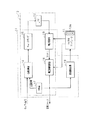
図1に示すように、このクロック生成装置は、大きくはクロック生成回路11と、ローパスフィルタ(LPF)12と、上記クロック生成回路11に接続された外部の制御装置としてのマイクロコンピュータ13とを備えて構成されている。また、上記クロック生成回路11の一部及びローパスフィルタ12によってPLL回路10が構成されている。
As shown in FIG. 1, the clock generation device generally includes a
ここで、上記クロック生成回路11は、位相比較器14、チャージポンプ15、電圧制御発振器16、分周器17、電圧制御器18及び周波数検出器19を1つのチップ上に備えて構成されている。
Here, the
このうち、位相比較器14は、光ディスク装置によって光ディスクから読み出される周期信号としてのウォブル信号を入力し、そのウォブル信号と電圧制御発振器16から出力される記録クロックが分周された分周信号との位相を比較してその位相差に応じた電圧をチャージポンプ15に出力する部分である。
Among these, the
また、チャージポンプ15は、位相比較器14からの位相差に応じた電圧をローパスフィルタ12に出力し、その位相差に比例した電圧をもってローパスフィルタ12の充・放電を制御する部分である。これにより、ローパスフィルタ12からは、チャージポンプ15の出力電圧に応じた制御電圧が電圧制御器18を介して電圧制御発振器16に出力されるようになる。
The charge pump 15 is a part that outputs a voltage corresponding to the phase difference from the
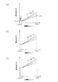
また、電圧制御発振器16は、入力される制御電圧に応じた周波数をもつクロックを発振する部分である。特に、この電圧制御発振器16は、入力される制御電圧と出力されるクロックの周波数(出力周波数)との関係である発振特性を複数有し、各発振特性毎に異なるオフセット周波数、及び電圧/周波数変換にかかるゲインが設定されている。詳しくは図2(a)〜(c)に示すように、この例では9種類(オフセット周波数3種類、ゲイン3種類)の発振特性C1〜C9がこの電圧制御発振器16に対して予め設定されている。このうち、図2(a)に示す発振特性C1〜C3は、オフセット周波数が同じでゲイン(傾き)が異なるよう設定されており、発振特性C3が最も高いゲインを有している。また、図2(b)及び(c)に示す発振特性C4〜C6及びC7〜C9は、図2(a)に例示した発振特性C1〜C3とそれぞれゲインが同じで、オフセット周波数のみが異なる関係になっている。
The voltage controlled
電圧制御発振器16に設定されているこれら発振特性C1〜C9は、上記マイクロコンピュータ13の制御によってそのいずれかが選択されるようになっている。詳しくは、上記複数のオフセット周波数及びゲインの中からその特定の組み合わせが選択的に設定されるようになっている。そして、電圧制御発振器16は、ローパスフィルタ12から電圧制御器18を介して制御電圧Vcntが与えられると、その制御電圧Vcntに応じた周波数のクロック(記録クロック)をマイクロコンピュータ13により設定された発振特性、すなわち上記発振特性C1〜C9のいずれかの発振特性にしたがって出力する。また、こ
の電圧制御発振器16から出力される記録クロックは、PLL回路10内において分周器17により所定に分周され、その分周された信号が位相比較器14の他方の入力として帰還される。すなわち、PLL回路10は、このようなフィードバック動作を繰り返し行うことにより、電圧制御発振器16から出力される記録クロック、正確にはその分周信号をウォブル信号に同期させる。
Any one of the oscillation characteristics C1 to C9 set in the voltage controlled
ところで、本実施の形態では、上記のごとく複数の発振特性C1〜C9をもってクロック発振の可能な電圧制御発振器16を用いているが、前述したように、この電圧制御発振器16に製造ばらつきがあるような場合には、設計上での特性と実際の特性とで異なる特性を示すことがある。そこで、本実施の形態では、クロック生成回路11内に上記電圧制御器18及び周波数検出器19を併せて備えることとし、これらを用いてマイクロコンピュータ13が電圧制御発振器16の上記各発振特性C1〜C9を同定(測定)したうえで、それら各発振特性C1〜C9のいずれかを選択的に設定するようにしている。以下、上記電圧制御器18及び周波数検出器19の構成、並びにこの同定手法について詳述する。
In the present embodiment, as described above, the voltage controlled
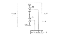
まず、電圧制御器18は、上記マイクロコンピュータ13による指令のもと、電圧制御発振器16に対して試験電圧を印加する回路である。詳しくは、この電圧制御器18は、図3に示すようなスイッチング回路からなり、マイクロコンピュータ13による制御によりスイッチS1がオンに、且つスイッチS2がオフとされることによって、電圧制御発振器16に印加する制御電圧Vcntをその最小の電圧(電位)である接地電圧Vgndとする。また、マイクロコンピュータ13によりスイッチS1がオフに、且つスイッチS2がオンとされることによって電圧制御発振器16に印加する制御電圧Vcntをその最大の電圧(電位)である電源電圧Vddとする。これらの場合、ローパスフィルタ12の出力はマイクロコンピュータ13によりハイインピーダンス出力とされ、制御電圧Vcntが確実に接地電圧Vgnd又は電源電圧Vddとなるようにしている。なお、通常は、上記スイッチS1及びS2がともにオフの状態に維持され、ローパスフィルタ12から出力される制御電圧Vcntがそのまま電圧制御発振器16に印加される。すなわち、ウォブル信号に同期した記録クロックを生成する際には、この電圧制御器18に設けられているスイッチS1及びS2がともにオフの状態に維持されるようにマイクロコンピュータ13によって制御される。
First, the
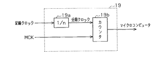
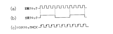
一方、周波数検出器19は、電圧制御発振器16から出力される記録クロックを入力し、その記録クロックの周波数を検出する回路である。詳しくは、この周波数検出器19は、図4に示すように所定の分周比を有する分周器19a及びカウンタ19bを備えて構成されている。そして、図5に示すように、電圧制御発振器16から発振される記録クロック(図5(a))を分周器19aにより分周した分周クロック(図5(b))と、外部の図示しない発振回路により生成されるマスタクロックMCK(図5(c))とをカウンタ19bにて比較することによって上記記録クロックの周波数を検出する。すなわち、カウンタ19bは、上記マスタクロックMCKの立ち上がりをカウントしており、上記分周クロックが例えば立ち上がる毎にその時々のマスタクロックMCKのカウント値をマイクロコンピュータ13に対して出力するとともに、カウント値をクリアして新たにカウントを開始する。
On the other hand, the
マイクロコンピュータ13には、上記分周器19aの分周比、及び上記マスタクロックMCKの周波数(周期)が予め与えられている。そして、同マイクロコンピュータ13では、この周波数検出器19のカウンタ19bから出力されるカウント値とこれら分周比、及びマスタクロックの周波数(周期)に基づいて、上記電圧制御発振器16から出力されている記録クロックの周波数を演算する。そして、この演算した周波数を、自身が備える記憶手段としてのメモリ13a(例えば、EEPROM等)に記憶する。
The
次に、電圧制御発振器16に設定されている発振特性C1〜C9の各オフセット周波数及びゲインを同定(測定)する具体的な処理について、図6に示すフローチャートに基づいて説明する。なお本実施の形態において、マイクロコンピュータ13は、以下に示す処理を光ディスク装置の起動毎に実行するものとする。
Next, specific processing for identifying (measuring) each offset frequency and gain of the oscillation characteristics C1 to C9 set in the voltage controlled
この同定処理に際し、マイクロコンピュータ13はまず、ステップS100の処理として、電圧制御発振器16の発振特性C1〜C9の中からいずれか1つを選択して同電圧制御発振器16に設定する。なお、ここでの例では、マイクロコンピュータ13が上記発振特性C1(図2(a)参照)に相当するオフセット周波数及びゲインを選択したとして以下説明する。
In this identification process, the
次に、マイクロコンピュータ13は、ステップS101の処理として、電圧制御器18のスイッチS2をオフにするとともに、スイッチS1(図3参照)をオンとするように制御し、電圧制御発振器16に試験電圧として、制御電圧Vcntがとりうる最小の電圧である上記接地電圧Vgndを印加する。これにより、先の図2(a)に示すように、電圧制御発振器16から周波数Foffのクロックが発振されるようになる。
Next, the
その後、マイクロコンピュータ13は、ステップS102の処理として、その周波数Foffを周波数検出器19のカウンタ19bから得られるカウント値に基づき検出し、さらにステップS103の処理として、この得られた周波数Foffをメモリ13aに記憶する。
After that, the
次に、マイクロコンピュータ13は、ステップS104の処理として、電圧制御器18のスイッチS1をオフにするとともに、スイッチS2をオンにする。これにより、電圧制御発振器16には試験電圧として、制御電圧Vcntがとりうる最大の電圧である上記電源電圧Vddが印加されることとなり、同じく先の図2(a)に示すように、電圧制御発振器16からは、当該発振特性C1において最大の周波数Fvddとなるクロックが発振されるようになる。そしてここでも、マイクロコンピュータ13は、ステップS105の処理として、この周波数Fvddを周波数検出器19のカウンタ19bから出力されるカウント値に基づき検出(演算)し、さらに、ステップS106の処理として、この得られた周波数Fvddをメモリ13aに記憶する。
Next, the
次に、マイクロコンピュータ13は、ステップS107の処理として、現在、電圧制御発振器16に設定されている発振特性C1についての同定を行う。すなわち、上記ステップS102及びS103において得られた周波数Foffをそのオフセット周波数として同定し、このオフセット周波数と上記ステップS105及びS106において得られた最大の周波数Fvddとの関係に基づきそのゲインを同定する。ちなみに、このゲインは、図2(a)に例示した発振特性C1の傾きとして求められる。なお、同図2(a)に示すように、発振特性には通常、接地電圧Vgndから約0.7V程度の不感帯が存在するため、マイクロコンピュータ13は、この不感帯を考慮してゲインを求めることとなる。そして、この求めたゲインについてもこれをメモリ13aに記憶して本処理を終了する。
Next, the
マイクロコンピュータ13はその後、他の発振特性C2〜C9についても同様に順次オフセット周波数及びゲインを設定して上述したステップS100〜S107の処理を繰り返し実行し、その結果同定された各発振特性C1〜C9のオフセット周波数及びゲインの全てをメモリ13aに一旦記憶する。
Thereafter, the
一方、実際に光ディスク装置によってDVD−RやDVD−RWへのデータ記録処理が行われる際には、光ディスク装置側からマイクロコンピュータ13に対して、例えば「4倍速での書き込み」等の指令が付与される。これにより、マイクロコンピュータ13は、
その指令に基づいて上記同定した発振特性C1〜C9の中から「4倍速での書き込み指令」に適した発振特性を選択してこれを電圧制御発振器16に設定する。詳しくは、光ディスクの回転速度(4倍速)から想定されるウォブル信号の周波数が発振可能な周波数範囲内にあって且つ、その周波数範囲の略中心になるとともに、よりゲインの小さい発振特性を上記同定した発振特性C1〜C9の中から選択して電圧制御発振器16に設定する。上記クロック生成回路11では、こうして電圧制御発振器16に設定された発振特性にしたがって、ウォブル信号に同期した記録クロックを自動生成することとなる。
On the other hand, when data recording processing to a DVD-R or DVD-RW is actually performed by the optical disc apparatus, a command such as “write at 4 × speed” is given to the
Based on the command, an oscillation characteristic suitable for the “write command at 4 × speed” is selected from the identified oscillation characteristics C1 to C9, and this is set in the voltage controlled
以上説明した実施の形態によれば、以下に列記する効果が得られるようになる。 According to the embodiment described above, the effects listed below can be obtained.
(1)複数の異なる発振特性をもってクロック発振の可能な電圧制御発振器16を用い、この電圧制御発振器16に対して試験電圧を与えてその製造ばらつきを含む実際の発振特性を同定することとした。そして、その同定した複数の発振特性の中からウォブル信号の想定される周波数がそれら発振特性において発振可能な周波数範囲内にあって且つ、その周波数範囲の略中心になるとともに、ゲインのより小さい発振特性を電圧制御発振器16に対して選択的に設定してクロックの生成を行うこととした。すなわち、電圧制御発振器16に製造ばらつきがあるような場合であれ、その複数の発振特性C1〜C9について上記試験電圧に基づき同定したうえで上記条件が満たされる発振特性を設定することとしたため、ジッターを含む各種周期信号に的確に同期するクロックを生成することができる。しかも、上記周期信号の想定される周波数がその発振可能な周波数範囲の略中心にあるものを選択するようにしたことで、周期信号の周波数のずれに対しても広い範囲で対応することができ、より安定した条件のもとで精度の高いクロックを生成することができるようになる。
(1) A voltage controlled
(2)マイクロコンピュータ13による制御のもと、上記試験電圧として、制御電圧Vcntのとりうる最小の電圧である接地電圧Vgnd及び最大の電圧である電源電圧Vddを電圧制御発振器16にそれぞれ印加して、そのときに発振されるクロックの周波数Foff及びFvddを周波数検出器19により検出するようにした。すなわち、電圧制御発振器16の発振特性としてその最小及び最大発振周波数の双方を検出するようにしたことで、各発振特性に対するオフセット周波数及びゲインを効率よく、しかも的確に同定することができる。
(2) Under the control of the
(3)電圧制御発振器16及び電圧制御器18がマイクロコンピュータ13により制御され、電圧制御発振器16が有する発振特性C1〜C9の同定に係る処理からこの同定に基づく電圧制御発振器16に対する発振特性の選択的な設定に至る一連の処理がマイクロコンピュータ13によってなされる構成とした。すなわち、発振特性の設定に至る処理がマイクロコンピュータ13のみで実行されるため、自由度の高い処理が可能になるとともに、それら処理の実行頻度も十分に確保することができる。
(3) The voltage controlled
(4)上記同定された各発振特性C1〜C9のオフセット周波数及びゲインがメモリ13aに記憶される構成とした。このため、それら同定された発振特性が記憶された後は、そのメモリ13aに記憶された各発振特性に基づき発振特性を選択設定することが可能となるため、発振特性の設定にかかる処理を迅速に行うことができるようになる。
(4) The configuration is such that the offset frequency and gain of each of the identified oscillation characteristics C1 to C9 are stored in the
(5)光ディスク装置の起動毎に各発振特性C1〜C9を同定することとした。このため、光ディスク装置を使用する環境が大きく変化する場合、あるいは電圧制御発振器16のばらつきの環境に対する依存性が高いような場合であれ、光ディスク装置の起動毎に使用環境に即したかたちで上記同定がなされるため、使用環境に順応することができる。
(5) The oscillation characteristics C1 to C9 are identified each time the optical disk device is started. For this reason, even if the environment in which the optical disk device is used changes greatly, or when the variation of the voltage-controlled
なお、上記実施の形態は以下のように変更して実施することもできる。 In addition, the said embodiment can also be changed and implemented as follows.
・上記実施の形態では、分周器17と周波数検出器19に設けられる分周器19aとを
各別に備える構成としたが、1つの分周器を共用する構成としてもよい。例えば、分周器17を共用する場合、その分周器17により分周された後の分周信号をカウンタ19bの一方の入力とすることができる。
In the above embodiment, the frequency divider 17 and the
・周波数検出器19の出力に基づく周波数演算は、例えばROMテーブル等に基づくマップ演算によって行うようにしてもよい。
The frequency calculation based on the output of the
・上記実施の形態では、光ディスク装置の起動毎にマイクロコンピュータ13により各発振特性について同定する処理を実行することとしたが、光ディスク装置を使用する環境が大きく変化しない場合、あるいは電圧制御発振器16のばらつきの環境に対する依存性が低いような場合には、例えば製品出荷時等に一度だけ上記同定を行う構成としてもよい。要は、同定に係る処理のタイミングや回数については特に限定されない。
In the above embodiment, each time the optical disk device is started, the
・上記実施の形態では、各発振特性C1〜C9の同定に際し、上記試験電圧として接地電圧Vgnd及び電源電圧Vddをそれぞれ電圧制御発振器16に印加することとしたが、これら最大電圧と最小電圧との中間電圧を同電圧制御発振器16に印加して各発振特性を同定するようにしてもよい。すなわち、各発振特性がオフセット周波数及びゲインの組み合わせからなるため、そのいずれか一方を正確なものとした場合には、こうした中間電圧を与えることでも電圧制御発振器16から出力されるクロックの周波数により他方のオフセット周波数またはゲインについて推定することができる。詳しくは、オフセット周波数が正確であるとした場合には、上記中間電圧を与えることにより得られる周波数及びオフセット周波数と、そのオフセット周波数に対応する最小電圧及び中間電圧とからその傾きとしてゲインが求まる。一方、ゲインが正確であるとした場合には、上記中間電圧を与えることにより得られる周波数をもとにそのゲイン、すなわち傾きからオフセット周波数が求まる。したがって、試験電圧として中間電圧を与えるのみでも各発振特性のオフセット周波数及びゲインを推定することができ、各発振特性の同定を簡易化することができるようになる。
In the above embodiment, when identifying the oscillation characteristics C1 to C9, the ground voltage Vgnd and the power supply voltage Vdd are applied to the voltage controlled
・上記実施の形態では、マイクロコンピュータ13のメモリ13aに上記同定された各発振特性C1〜C9のオフセット周波数及びゲインを記憶することとしたが、クロック生成回路11内やクロック生成回路11の外部に設けたメモリ(記憶手段)に上記同定された各発振特性C1〜C9を記憶する構成としてもよい。こうすることで、例えばクロック生成回路11にマイクロコンピュータ13を組み付けた時点で既にそのメモリ(記憶手段)に記憶されている同定情報に基づいて発振特性C1〜C9の選択を行うことができるようになる。
In the above embodiment, the offset frequency and gain of each of the identified oscillation characteristics C1 to C9 are stored in the
・上記実施の形態では、発振可能な周波数範囲の略中心にウォブル信号の想定される周波数が位置する発振特性を発振特性C1〜C9の中から選択的に設定することとしたが、必ずしもウォブル信号の周波数が周波数範囲の略中心となる発振特性である必要はなく、ウォブル信号の周波数が周波数範囲内に収まる発振特性であればよい。 In the above embodiment, the oscillation characteristic in which the assumed frequency of the wobble signal is located at the approximate center of the oscillating frequency range is selectively set from the oscillation characteristics C1 to C9. The oscillation characteristics need not be the center of the frequency range, and may be any oscillation characteristic that allows the frequency of the wobble signal to fall within the frequency range.
・上記実施の形態では、光ディスクへのデータ記録処理の際に基準となる記録クロックを生成する装置に本発明を適用する場合について示したが、光ディスクからデータを再生する再生処理の際に基準となる再生クロックを生成する装置にも本発明を同様に適用することができる。 In the above-described embodiment, the case where the present invention is applied to an apparatus that generates a recording clock serving as a reference in data recording processing on an optical disc has been described. The present invention can be similarly applied to an apparatus for generating a regenerated clock.
・上記実施の形態では、DVD−R/RWにデータを記録する際の記録クロックを生成する装置に本発明を適用する場合について示したが、DVD系ディスク、CD−R/RW、Blu−rayディスク等の他の光ディスクにデータを記録する際の記録クロックを生成する装置についても本発明を同様に適用することができる。要は、周期信号に同期したクロックの生成が望まれる全ての光ディスク装置について本発明は適用可能である。 In the above embodiment, the case where the present invention is applied to an apparatus that generates a recording clock when recording data on a DVD-R / RW has been described. However, a DVD-based disc, a CD-R / RW, a Blu-ray The present invention can be similarly applied to an apparatus that generates a recording clock when recording data on another optical disk such as a disk. In short, the present invention can be applied to all optical disc apparatuses in which generation of a clock synchronized with a periodic signal is desired.
・上記実施の形態では、クロック生成装置として、電圧制御発振器16、電圧制御器18等を備えるクロック生成回路11やマイクロコンピュータ13等を備えて構成されるものについて示したが、同クロック生成装置としては、少なくともクロック生成回路11を1つのチップ上に備えるものであればよい。また特に、電圧制御発振器16の発振特性についてその同定を行うことのできる構成ということであれば、クロック生成装置として、少なくともこの電圧制御発振器16をはじめ、電圧制御器18及び周波数検出器19を備えることで足りる。すなわち、電圧制御器18を備えることで電圧制御発振器16に対して任意に試験電圧を与えることができ、周波数検出器19を備えることで、その与えられた試験電圧に基づく電圧制御発振器16の発振特性を適宜にモニタすることはできる。
In the above-described embodiment, the clock generation device is described as including the
10…PLL回路、11…クロック生成回路、12…ローパスフィルタ(LPF)、13…マイクロコンピュータ、13a…メモリ、14…位相比較器、15…チャージポンプ、16…電圧制御発振器、17…分周器、18…電圧制御器、19…周波数検出器。19a…分周器、19b…カウンタ、S1,S2…スイッチ。
DESCRIPTION OF
Claims (8)
前記電圧制御発振器に設定されている発振特性を順次選択しつつ、同電圧制御発振器に試験電圧を与えて、それら発振特性の各々を同定し、該同定した各発振特性のうち、前記同期の対象とする周期信号の想定される周波数がそれら発振特性において発振可能な周波数範囲内にあって且つ、ゲインのより小さい発振特性を前記電圧制御発振器に設定して前記クロックの生成を行う
ことを特徴とするクロック生成方法。 A clock generation method for generating a clock synchronized with a periodic signal using a voltage controlled oscillator capable of clock oscillation with a plurality of different oscillation characteristics with respect to an applied control voltage,
While sequentially selecting the oscillation characteristics set in the voltage controlled oscillator, a test voltage is applied to the voltage controlled oscillator to identify each of the oscillation characteristics, and among the identified oscillation characteristics, the synchronization target The clock signal is generated by setting an oscillation characteristic having a smaller gain within the frequency range in which the periodic signal can be oscillated in the oscillation characteristic and having a smaller gain in the voltage-controlled oscillator. Clock generation method.
請求項1に記載のクロック生成方法。 The sequentially selected oscillation characteristics comprise a combination of a plurality of offset frequencies and a plurality of gains for voltage / frequency conversion, and the identification for each oscillation characteristic is the maximum voltage that the control voltage can take as the test voltage. And a frequency of a clock output from the voltage controlled oscillator when the minimum voltage is applied to the voltage controlled oscillator, respectively, and the detected two frequency values and the applied two voltage values are detected. The clock generation method according to claim 1, wherein each is performed by specifying the offset frequency and the gain.
請求項1に記載のクロック生成方法。 The sequentially selected oscillation characteristics comprise a combination of a plurality of offset frequencies and a plurality of gains for voltage / frequency conversion, and the identification for each oscillation characteristic is the maximum voltage that the control voltage can take as the test voltage. And a frequency of a clock output from the voltage-controlled oscillator when an intermediate voltage of the minimum voltage is applied to the voltage-controlled oscillator, and the offset is determined from the detected frequency value and the applied voltage value, respectively. The clock generation method according to claim 1, wherein the clock generation method is performed by estimating a frequency and the gain.
印加される制御電圧に対し複数の異なる発振特性をもってクロック発振の可能な電圧制御発振器と、この電圧制御発振器に設定されている発振特性の順次の選択に伴って同電圧制御発振器に試験電圧を与える電圧制御器と、前記試験電圧の付与によって前記電圧制御発振器から出力されるクロックの周波数を検出する周波数検出器とを備える
ことを特徴とするクロック生成装置。 A clock generator for inputting a periodic signal and generating a clock synchronized with the periodic signal,
A voltage-controlled oscillator capable of clock oscillation with a plurality of different oscillation characteristics with respect to the applied control voltage, and a test voltage is applied to the voltage-controlled oscillator as the oscillation characteristics set in the voltage-controlled oscillator are sequentially selected. A clock generation apparatus comprising: a voltage controller; and a frequency detector that detects a frequency of a clock output from the voltage controlled oscillator when the test voltage is applied.
前記電圧制御発振器に設定されている発振特性の順次選択に伴い前記電圧制御器から前記電圧制御発振器に付与される試験電圧の値とこの試験電圧に対応して前記周波数検出器によって検出される周波数の値とに基づいて前記電圧制御発振器に設定されている発振特性の各々が同定されるとともに、該同定された各発振特性のうち、前記同期の対象とする周期信号の想定される周波数がそれら発振特性において発振可能な周波数範囲内にあって且つ、ゲインのより小さい発振特性が、前記周期信号に同期したクロックを生成するための発振特性として前記電圧制御発振器に選択的に設定される
ことを特徴とするクロック生成装置。 The clock generator according to claim 4, wherein
A value of a test voltage applied from the voltage controller to the voltage controlled oscillator with the sequential selection of oscillation characteristics set in the voltage controlled oscillator and a frequency detected by the frequency detector corresponding to the test voltage Each of the oscillation characteristics set in the voltage-controlled oscillator is identified based on the value of the oscillation frequency, and among the identified oscillation characteristics, the assumed frequency of the periodic signal to be synchronized is An oscillation characteristic within a frequency range where oscillation can be oscillated and whose gain is smaller is selectively set in the voltage controlled oscillator as an oscillation characteristic for generating a clock synchronized with the periodic signal. A clock generation device.
請求項5に記載のクロック生成装置。 The sequentially selected oscillation characteristics comprise a combination of a plurality of offset frequencies and a plurality of gains for voltage / frequency conversion, and the identification for each oscillation characteristic is the maximum voltage that the control voltage can take as the test voltage. And the minimum voltage is applied to the voltage controlled oscillator and the frequency of the clock output from the voltage controlled oscillator is detected by the frequency detector, respectively, and the value of the two detected frequencies and the given The clock generation device according to claim 5, wherein the clock generation device is performed by specifying the offset frequency and the gain from the values of two voltages that are generated.
同定は、前記試験電圧として前記制御電圧がとりうる最大電圧及び最小電圧の中間電圧が電圧制御発振器に与えられて且つ、同電圧制御発振器から出力されるクロックの周波数が前記周波数検出器によって検出されたときの、該検出される周波数の値と前記与えられる電圧の値とから各々前記オフセット周波数及び前記ゲインが推定されることによって行われる
請求項5に記載のクロック生成装置。 The sequentially selected oscillation characteristics comprise a combination of a plurality of offset frequencies and a plurality of gains for voltage / frequency conversion, and the identification for each oscillation characteristic is the maximum voltage that the control voltage can take as the test voltage. And an intermediate voltage of the minimum voltage is applied to the voltage controlled oscillator, and a value of the detected frequency when the frequency of the clock output from the voltage controlled oscillator is detected by the frequency detector is given. The clock generation device according to claim 5, which is performed by estimating the offset frequency and the gain from a voltage value.
請求項4〜7のいずれか一項に記載のクロック生成装置。 The periodic signal to be synchronized is one of periodic signals extracted from the optical disc, and the identification of the oscillation characteristic and the selective setting of the oscillation characteristic for the voltage controlled oscillator based on the identification are performed on the optical disc. The clock generation device according to any one of claims 4 to 7, wherein the clock generation device is executed each time the optical disk device that performs data recording / reproduction with respect to the optical disk device is started.
Priority Applications (5)
| Application Number | Priority Date | Filing Date | Title |
|---|---|---|---|
| JP2004022818A JP4260034B2 (en) | 2004-01-30 | 2004-01-30 | Clock generation method and clock generation apparatus |
| CN2005100043737A CN1652466B (en) | 2004-01-30 | 2005-01-17 | Method and device for generating clock signal |
| US11/044,736 US7141961B2 (en) | 2004-01-30 | 2005-01-27 | Method and device for generating clock signal |
| TW094102416A TWI267722B (en) | 2004-01-30 | 2005-01-27 | Clock generating method and clock generating apparatus |
| KR1020050007866A KR100767167B1 (en) | 2004-01-30 | 2005-01-28 | Clock generating method and clock generating device |
Applications Claiming Priority (1)
| Application Number | Priority Date | Filing Date | Title |
|---|---|---|---|
| JP2004022818A JP4260034B2 (en) | 2004-01-30 | 2004-01-30 | Clock generation method and clock generation apparatus |
Publications (2)
| Publication Number | Publication Date |
|---|---|
| JP2005217841A true JP2005217841A (en) | 2005-08-11 |
| JP4260034B2 JP4260034B2 (en) | 2009-04-30 |
Family
ID=34805680
Family Applications (1)
| Application Number | Title | Priority Date | Filing Date |
|---|---|---|---|
| JP2004022818A Expired - Fee Related JP4260034B2 (en) | 2004-01-30 | 2004-01-30 | Clock generation method and clock generation apparatus |
Country Status (5)
| Country | Link |
|---|---|
| US (1) | US7141961B2 (en) |
| JP (1) | JP4260034B2 (en) |
| KR (1) | KR100767167B1 (en) |
| CN (1) | CN1652466B (en) |
| TW (1) | TWI267722B (en) |
Families Citing this family (22)
| Publication number | Priority date | Publication date | Assignee | Title |
|---|---|---|---|---|
| JP4925630B2 (en) * | 2005-09-06 | 2012-05-09 | 株式会社アドバンテスト | Test apparatus and test method |
| US20070266263A1 (en) * | 2006-05-11 | 2007-11-15 | Silicon Integrated Systems Corp. | Speed adjustment system and method for performing the same |
| KR101354836B1 (en) * | 2006-08-25 | 2014-01-22 | 엘지전자 주식회사 | Frequency phasing apparatus and method of controlling the same |
| JP4538476B2 (en) * | 2007-08-27 | 2010-09-08 | 独立行政法人理化学研究所 | Method for forming a semiconductor structure |
| JP2009054782A (en) * | 2007-08-27 | 2009-03-12 | Institute Of Physical & Chemical Research | Optical semiconductor device and manufacturing method thereof |
| JP2011130604A (en) | 2009-12-18 | 2011-06-30 | Sanyo Electric Co Ltd | Charging circuit and amplifying circuit |
| US9083356B1 (en) | 2013-03-14 | 2015-07-14 | Gsi Technology, Inc. | Systems and methods of phase-locked loop involving closed-loop, continuous frequency range, auto calibration and/or other features |
| US10854284B1 (en) | 2016-12-06 | 2020-12-01 | Gsi Technology, Inc. | Computational memory cell and processing array device with ratioless write port |
| US10860320B1 (en) | 2016-12-06 | 2020-12-08 | Gsi Technology, Inc. | Orthogonal data transposition system and method during data transfers to/from a processing array |
| US10777262B1 (en) | 2016-12-06 | 2020-09-15 | Gsi Technology, Inc. | Read data processing circuits and methods associated memory cells |
| US10847213B1 (en) | 2016-12-06 | 2020-11-24 | Gsi Technology, Inc. | Write data processing circuits and methods associated with computational memory cells |
| US10725777B2 (en) | 2016-12-06 | 2020-07-28 | Gsi Technology, Inc. | Computational memory cell and processing array device using memory cells |
| US10770133B1 (en) | 2016-12-06 | 2020-09-08 | Gsi Technology, Inc. | Read and write data processing circuits and methods associated with computational memory cells that provides write inhibits and read bit line pre-charge inhibits |
| US10847212B1 (en) | 2016-12-06 | 2020-11-24 | Gsi Technology, Inc. | Read and write data processing circuits and methods associated with computational memory cells using two read multiplexers |
| US10891076B1 (en) | 2016-12-06 | 2021-01-12 | Gsi Technology, Inc. | Results processing circuits and methods associated with computational memory cells |
| US10998040B2 (en) | 2016-12-06 | 2021-05-04 | Gsi Technology, Inc. | Computational memory cell and processing array device using the memory cells for XOR and XNOR computations |
| US10943648B1 (en) | 2016-12-06 | 2021-03-09 | Gsi Technology, Inc. | Ultra low VDD memory cell with ratioless write port |
| US11227653B1 (en) | 2016-12-06 | 2022-01-18 | Gsi Technology, Inc. | Storage array circuits and methods for computational memory cells |
| JP6828484B2 (en) * | 2017-02-08 | 2021-02-10 | 株式会社デンソー | PLL circuit for radar |
| US10930341B1 (en) | 2019-06-18 | 2021-02-23 | Gsi Technology, Inc. | Processing array device that performs one cycle full adder operation and bit line read/write logic features |
| US10958272B2 (en) | 2019-06-18 | 2021-03-23 | Gsi Technology, Inc. | Computational memory cell and processing array device using complementary exclusive or memory cells |
| US10877731B1 (en) | 2019-06-18 | 2020-12-29 | Gsi Technology, Inc. | Processing array device that performs one cycle full adder operation and bit line read/write logic features |
Family Cites Families (6)
| Publication number | Priority date | Publication date | Assignee | Title |
|---|---|---|---|---|
| JP3208736B2 (en) * | 1991-11-08 | 2001-09-17 | ソニー株式会社 | PLL circuit |
| JPH1131966A (en) * | 1997-06-03 | 1999-02-02 | Motorola Inc | Device and tuning method regarding voltage-controlled oscillator |
| JP2944607B2 (en) * | 1998-02-12 | 1999-09-06 | 日本電気アイシーマイコンシステム株式会社 | Digital PLL circuit and clock generation method |
| JP2000278124A (en) * | 1999-03-26 | 2000-10-06 | Sanyo Electric Co Ltd | Pll circuit |
| US6292507B1 (en) * | 1999-09-01 | 2001-09-18 | Lexmark International, Inc. | Method and apparatus for compensating a spread spectrum clock generator |
| JP2001076437A (en) * | 1999-09-06 | 2001-03-23 | Victor Co Of Japan Ltd | Clock signal generator |
-
2004
- 2004-01-30 JP JP2004022818A patent/JP4260034B2/en not_active Expired - Fee Related
-
2005
- 2005-01-17 CN CN2005100043737A patent/CN1652466B/en not_active Expired - Fee Related
- 2005-01-27 TW TW094102416A patent/TWI267722B/en not_active IP Right Cessation
- 2005-01-27 US US11/044,736 patent/US7141961B2/en not_active Expired - Lifetime
- 2005-01-28 KR KR1020050007866A patent/KR100767167B1/en not_active Expired - Fee Related
Also Published As
| Publication number | Publication date |
|---|---|
| KR100767167B1 (en) | 2007-10-15 |
| JP4260034B2 (en) | 2009-04-30 |
| TWI267722B (en) | 2006-12-01 |
| CN1652466A (en) | 2005-08-10 |
| US7141961B2 (en) | 2006-11-28 |
| TW200528958A (en) | 2005-09-01 |
| US20050168253A1 (en) | 2005-08-04 |
| KR20050078223A (en) | 2005-08-04 |
| CN1652466B (en) | 2010-04-28 |
Similar Documents
| Publication | Publication Date | Title |
|---|---|---|
| JP4260034B2 (en) | Clock generation method and clock generation apparatus | |
| JP3910986B2 (en) | Optical disk device | |
| JPH1173645A (en) | Optical disk drive | |
| US7065017B2 (en) | Optical disk apparatus, method for generating clock signal of optical disk apparatus, and method for setting amount of light of optical disk apparatus | |
| US7304523B2 (en) | Clock generating apparatus and method in optical storage system | |
| JP2004159161A (en) | Delay signal generation device and write pulse generation device | |
| JP3820856B2 (en) | Optical disk recording device | |
| CN100452181C (en) | PLL clock generator, its control method and optical disc device | |
| CN101547006B (en) | Phase synchronization circuit | |
| KR100585899B1 (en) | Pll circuit | |
| US6914465B2 (en) | Voltage-controlled osillator | |
| US6992958B2 (en) | Phase-locked loop circuit for reproducing a channel clock | |
| JP2002230752A (en) | Wobble defect detection apparatus and method | |
| JP3649955B2 (en) | Clock signal generator for data recording | |
| US7038987B2 (en) | Optical disk device | |
| KR100213261B1 (en) | Frequency detector of PLL | |
| JP2004253057A (en) | Clock producing device | |
| JP2001357620A (en) | Optical disk recording device and its semiconductor integrated circuit | |
| JP2005510001A (en) | An apparatus for recording or reproducing information, comprising means for generating a signal from a wobble signal | |
| JP4494941B2 (en) | Clock signal generator for data recording | |
| JP2004178655A (en) | Clock generating circuit and recording / reproducing apparatus using the same | |
| US20070205737A1 (en) | Control circuit and method of controlling rotation frequency of spindle in optical disc drive for reducing frequency difference of output signals respectively corresponding to different disc rotation modes | |
| JP2004343724A (en) | PLL clock generator, optical disk apparatus, and control method for PLL clock generator | |
| JP2005071606A (en) | Clock signal generator for data recording | |
| JP2002230757A (en) | Clock generating circuit and recording / reproducing apparatus using the same |
Legal Events
| Date | Code | Title | Description |
|---|---|---|---|
| RD01 | Notification of change of attorney |
Free format text: JAPANESE INTERMEDIATE CODE: A7421 Effective date: 20051227 |
|
| A621 | Written request for application examination |
Free format text: JAPANESE INTERMEDIATE CODE: A621 Effective date: 20070112 |
|
| A977 | Report on retrieval |
Free format text: JAPANESE INTERMEDIATE CODE: A971007 Effective date: 20081003 |
|
| A131 | Notification of reasons for refusal |
Free format text: JAPANESE INTERMEDIATE CODE: A131 Effective date: 20081014 |
|
| A521 | Request for written amendment filed |
Free format text: JAPANESE INTERMEDIATE CODE: A523 Effective date: 20081204 |
|
| TRDD | Decision of grant or rejection written | ||
| A01 | Written decision to grant a patent or to grant a registration (utility model) |
Free format text: JAPANESE INTERMEDIATE CODE: A01 Effective date: 20090106 |
|
| A01 | Written decision to grant a patent or to grant a registration (utility model) |
Free format text: JAPANESE INTERMEDIATE CODE: A01 |
|
| A61 | First payment of annual fees (during grant procedure) |
Free format text: JAPANESE INTERMEDIATE CODE: A61 Effective date: 20090203 |
|
| FPAY | Renewal fee payment (event date is renewal date of database) |
Free format text: PAYMENT UNTIL: 20120220 Year of fee payment: 3 |
|
| R151 | Written notification of patent or utility model registration |
Ref document number: 4260034 Country of ref document: JP Free format text: JAPANESE INTERMEDIATE CODE: R151 |
|
| FPAY | Renewal fee payment (event date is renewal date of database) |
Free format text: PAYMENT UNTIL: 20120220 Year of fee payment: 3 |
|
| FPAY | Renewal fee payment (event date is renewal date of database) |
Free format text: PAYMENT UNTIL: 20130220 Year of fee payment: 4 |
|
| R250 | Receipt of annual fees |
Free format text: JAPANESE INTERMEDIATE CODE: R250 |
|
| FPAY | Renewal fee payment (event date is renewal date of database) |
Free format text: PAYMENT UNTIL: 20140220 Year of fee payment: 5 |
|
| R250 | Receipt of annual fees |
Free format text: JAPANESE INTERMEDIATE CODE: R250 |
|
| R250 | Receipt of annual fees |
Free format text: JAPANESE INTERMEDIATE CODE: R250 |
|
| R250 | Receipt of annual fees |
Free format text: JAPANESE INTERMEDIATE CODE: R250 |
|
| R250 | Receipt of annual fees |
Free format text: JAPANESE INTERMEDIATE CODE: R250 |
|
| R250 | Receipt of annual fees |
Free format text: JAPANESE INTERMEDIATE CODE: R250 |
|
| R250 | Receipt of annual fees |
Free format text: JAPANESE INTERMEDIATE CODE: R250 |
|
| R250 | Receipt of annual fees |
Free format text: JAPANESE INTERMEDIATE CODE: R250 |
|
| R250 | Receipt of annual fees |
Free format text: JAPANESE INTERMEDIATE CODE: R250 |
|
| R250 | Receipt of annual fees |
Free format text: JAPANESE INTERMEDIATE CODE: R250 |
|
| LAPS | Cancellation because of no payment of annual fees |