JP2004128498A - コンデンサ構造及びこれをジュアルダマスカス過程にて製造する方法 - Google Patents
コンデンサ構造及びこれをジュアルダマスカス過程にて製造する方法 Download PDFInfo
- Publication number
- JP2004128498A JP2004128498A JP2003334485A JP2003334485A JP2004128498A JP 2004128498 A JP2004128498 A JP 2004128498A JP 2003334485 A JP2003334485 A JP 2003334485A JP 2003334485 A JP2003334485 A JP 2003334485A JP 2004128498 A JP2004128498 A JP 2004128498A
- Authority
- JP
- Japan
- Prior art keywords
- capacitor
- conductive
- forming
- bottom plate
- dielectric layer
- Prior art date
- Legal status (The legal status is an assumption and is not a legal conclusion. Google has not performed a legal analysis and makes no representation as to the accuracy of the status listed.)
- Granted
Links
- 239000003990 capacitor Substances 0.000 title claims abstract description 88
- 238000000034 method Methods 0.000 title claims abstract description 33
- 230000009977 dual effect Effects 0.000 title claims abstract description 32
- 238000004519 manufacturing process Methods 0.000 title abstract description 16
- 239000000758 substrate Substances 0.000 claims description 28
- 239000004065 semiconductor Substances 0.000 claims description 21
- RYGMFSIKBFXOCR-UHFFFAOYSA-N Copper Chemical compound [Cu] RYGMFSIKBFXOCR-UHFFFAOYSA-N 0.000 claims description 17
- 229910052802 copper Inorganic materials 0.000 claims description 17
- 239000010949 copper Substances 0.000 claims description 17
- 239000000463 material Substances 0.000 claims description 13
- 239000004020 conductor Substances 0.000 claims description 11
- VYPSYNLAJGMNEJ-UHFFFAOYSA-N Silicium dioxide Chemical compound O=[Si]=O VYPSYNLAJGMNEJ-UHFFFAOYSA-N 0.000 claims description 8
- RTAQQCXQSZGOHL-UHFFFAOYSA-N Titanium Chemical group [Ti] RTAQQCXQSZGOHL-UHFFFAOYSA-N 0.000 claims description 7
- 239000010936 titanium Substances 0.000 claims description 7
- 229910052719 titanium Inorganic materials 0.000 claims description 7
- NRTOMJZYCJJWKI-UHFFFAOYSA-N Titanium nitride Chemical compound [Ti]#N NRTOMJZYCJJWKI-UHFFFAOYSA-N 0.000 claims description 6
- 229910052782 aluminium Inorganic materials 0.000 claims description 6
- XAGFODPZIPBFFR-UHFFFAOYSA-N aluminium Chemical compound [Al] XAGFODPZIPBFFR-UHFFFAOYSA-N 0.000 claims description 6
- 229910052454 barium strontium titanate Inorganic materials 0.000 claims description 4
- 229910002113 barium titanate Inorganic materials 0.000 claims description 4
- JRPBQTZRNDNNOP-UHFFFAOYSA-N barium titanate Chemical compound [Ba+2].[Ba+2].[O-][Ti]([O-])([O-])[O-] JRPBQTZRNDNNOP-UHFFFAOYSA-N 0.000 claims description 4
- BPUBBGLMJRNUCC-UHFFFAOYSA-N oxygen(2-);tantalum(5+) Chemical compound [O-2].[O-2].[O-2].[O-2].[O-2].[Ta+5].[Ta+5] BPUBBGLMJRNUCC-UHFFFAOYSA-N 0.000 claims description 4
- 235000012239 silicon dioxide Nutrition 0.000 claims description 4
- 239000000377 silicon dioxide Substances 0.000 claims description 4
- VEALVRVVWBQVSL-UHFFFAOYSA-N strontium titanate Chemical compound [Sr+2].[O-][Ti]([O-])=O VEALVRVVWBQVSL-UHFFFAOYSA-N 0.000 claims description 4
- MZLGASXMSKOWSE-UHFFFAOYSA-N tantalum nitride Chemical compound [Ta]#N MZLGASXMSKOWSE-UHFFFAOYSA-N 0.000 claims description 4
- PBCFLUZVCVVTBY-UHFFFAOYSA-N tantalum pentoxide Inorganic materials O=[Ta](=O)O[Ta](=O)=O PBCFLUZVCVVTBY-UHFFFAOYSA-N 0.000 claims description 4
- BLRPTPMANUNPDV-UHFFFAOYSA-N Silane Chemical compound [SiH4] BLRPTPMANUNPDV-UHFFFAOYSA-N 0.000 claims description 3
- 229910000449 hafnium oxide Inorganic materials 0.000 claims description 3
- WIHZLLGSGQNAGK-UHFFFAOYSA-N hafnium(4+);oxygen(2-) Chemical compound [O-2].[O-2].[Hf+4] WIHZLLGSGQNAGK-UHFFFAOYSA-N 0.000 claims description 3
- 229910000077 silane Inorganic materials 0.000 claims description 3
- 239000003989 dielectric material Substances 0.000 abstract description 2
- 230000004888 barrier function Effects 0.000 description 17
- 229910052751 metal Inorganic materials 0.000 description 12
- 239000002184 metal Substances 0.000 description 12
- 230000000873 masking effect Effects 0.000 description 7
- 239000010409 thin film Substances 0.000 description 6
- 238000005530 etching Methods 0.000 description 5
- 238000001465 metallisation Methods 0.000 description 5
- 238000009792 diffusion process Methods 0.000 description 4
- 230000015572 biosynthetic process Effects 0.000 description 3
- 238000005229 chemical vapour deposition Methods 0.000 description 3
- 230000000694 effects Effects 0.000 description 3
- 238000000059 patterning Methods 0.000 description 3
- 229910021420 polycrystalline silicon Inorganic materials 0.000 description 3
- WFKWXMTUELFFGS-UHFFFAOYSA-N tungsten Chemical compound [W] WFKWXMTUELFFGS-UHFFFAOYSA-N 0.000 description 3
- 229910052721 tungsten Inorganic materials 0.000 description 3
- 239000010937 tungsten Substances 0.000 description 3
- 229910052581 Si3N4 Inorganic materials 0.000 description 2
- XUIMIQQOPSSXEZ-UHFFFAOYSA-N Silicon Chemical compound [Si] XUIMIQQOPSSXEZ-UHFFFAOYSA-N 0.000 description 2
- 238000000151 deposition Methods 0.000 description 2
- 230000008021 deposition Effects 0.000 description 2
- 230000001788 irregular Effects 0.000 description 2
- BASFCYQUMIYNBI-UHFFFAOYSA-N platinum Chemical compound [Pt] BASFCYQUMIYNBI-UHFFFAOYSA-N 0.000 description 2
- 229920005591 polysilicon Polymers 0.000 description 2
- 229910052710 silicon Inorganic materials 0.000 description 2
- 239000010703 silicon Substances 0.000 description 2
- HQVNEWCFYHHQES-UHFFFAOYSA-N silicon nitride Chemical compound N12[Si]34N5[Si]62N3[Si]51N64 HQVNEWCFYHHQES-UHFFFAOYSA-N 0.000 description 2
- 229910000881 Cu alloy Inorganic materials 0.000 description 1
- 239000000969 carrier Substances 0.000 description 1
- -1 e.g. Substances 0.000 description 1
- 238000009713 electroplating Methods 0.000 description 1
- 230000001747 exhibiting effect Effects 0.000 description 1
- 230000002349 favourable effect Effects 0.000 description 1
- 239000012535 impurity Substances 0.000 description 1
- 150000002739 metals Chemical class 0.000 description 1
- 230000003071 parasitic effect Effects 0.000 description 1
- 238000005240 physical vapour deposition Methods 0.000 description 1
- 229910052697 platinum Inorganic materials 0.000 description 1
- 238000005498 polishing Methods 0.000 description 1
- HBMJWWWQQXIZIP-UHFFFAOYSA-N silicon carbide Chemical compound [Si+]#[C-] HBMJWWWQQXIZIP-UHFFFAOYSA-N 0.000 description 1
- 229910010271 silicon carbide Inorganic materials 0.000 description 1
- 238000004544 sputter deposition Methods 0.000 description 1
- 239000000126 substance Substances 0.000 description 1
- 229910052715 tantalum Inorganic materials 0.000 description 1
- GUVRBAGPIYLISA-UHFFFAOYSA-N tantalum atom Chemical compound [Ta] GUVRBAGPIYLISA-UHFFFAOYSA-N 0.000 description 1
Images


Classifications
-
- H—ELECTRICITY
- H01—ELECTRIC ELEMENTS
- H01L—SEMICONDUCTOR DEVICES NOT COVERED BY CLASS H10
- H01L28/00—Passive two-terminal components without a potential-jump or surface barrier for integrated circuits; Details thereof; Multistep manufacturing processes therefor
- H01L28/40—Capacitors
- H01L28/60—Electrodes
-
- H—ELECTRICITY
- H01—ELECTRIC ELEMENTS
- H01L—SEMICONDUCTOR DEVICES NOT COVERED BY CLASS H10
- H01L27/00—Devices consisting of a plurality of semiconductor or other solid-state components formed in or on a common substrate
- H01L27/02—Devices consisting of a plurality of semiconductor or other solid-state components formed in or on a common substrate including semiconductor components specially adapted for rectifying, oscillating, amplifying or switching and having potential barriers; including integrated passive circuit elements having potential barriers
- H01L27/04—Devices consisting of a plurality of semiconductor or other solid-state components formed in or on a common substrate including semiconductor components specially adapted for rectifying, oscillating, amplifying or switching and having potential barriers; including integrated passive circuit elements having potential barriers the substrate being a semiconductor body
-
- H—ELECTRICITY
- H01—ELECTRIC ELEMENTS
- H01L—SEMICONDUCTOR DEVICES NOT COVERED BY CLASS H10
- H01L23/00—Details of semiconductor or other solid state devices
- H01L23/52—Arrangements for conducting electric current within the device in operation from one component to another, i.e. interconnections, e.g. wires, lead frames
- H01L23/522—Arrangements for conducting electric current within the device in operation from one component to another, i.e. interconnections, e.g. wires, lead frames including external interconnections consisting of a multilayer structure of conductive and insulating layers inseparably formed on the semiconductor body
- H01L23/5222—Capacitive arrangements or effects of, or between wiring layers
- H01L23/5223—Capacitor integral with wiring layers
-
- H—ELECTRICITY
- H01—ELECTRIC ELEMENTS
- H01L—SEMICONDUCTOR DEVICES NOT COVERED BY CLASS H10
- H01L21/00—Processes or apparatus adapted for the manufacture or treatment of semiconductor or solid state devices or of parts thereof
- H01L21/70—Manufacture or treatment of devices consisting of a plurality of solid state components formed in or on a common substrate or of parts thereof; Manufacture of integrated circuit devices or of parts thereof
- H01L21/71—Manufacture of specific parts of devices defined in group H01L21/70
- H01L21/768—Applying interconnections to be used for carrying current between separate components within a device comprising conductors and dielectrics
- H01L21/76801—Applying interconnections to be used for carrying current between separate components within a device comprising conductors and dielectrics characterised by the formation and the after-treatment of the dielectrics, e.g. smoothing
- H01L21/76802—Applying interconnections to be used for carrying current between separate components within a device comprising conductors and dielectrics characterised by the formation and the after-treatment of the dielectrics, e.g. smoothing by forming openings in dielectrics
- H01L21/76805—Applying interconnections to be used for carrying current between separate components within a device comprising conductors and dielectrics characterised by the formation and the after-treatment of the dielectrics, e.g. smoothing by forming openings in dielectrics the opening being a via or contact hole penetrating the underlying conductor
-
- H—ELECTRICITY
- H01—ELECTRIC ELEMENTS
- H01L—SEMICONDUCTOR DEVICES NOT COVERED BY CLASS H10
- H01L21/00—Processes or apparatus adapted for the manufacture or treatment of semiconductor or solid state devices or of parts thereof
- H01L21/70—Manufacture or treatment of devices consisting of a plurality of solid state components formed in or on a common substrate or of parts thereof; Manufacture of integrated circuit devices or of parts thereof
- H01L21/71—Manufacture of specific parts of devices defined in group H01L21/70
- H01L21/768—Applying interconnections to be used for carrying current between separate components within a device comprising conductors and dielectrics
- H01L21/76801—Applying interconnections to be used for carrying current between separate components within a device comprising conductors and dielectrics characterised by the formation and the after-treatment of the dielectrics, e.g. smoothing
- H01L21/76802—Applying interconnections to be used for carrying current between separate components within a device comprising conductors and dielectrics characterised by the formation and the after-treatment of the dielectrics, e.g. smoothing by forming openings in dielectrics
- H01L21/76807—Applying interconnections to be used for carrying current between separate components within a device comprising conductors and dielectrics characterised by the formation and the after-treatment of the dielectrics, e.g. smoothing by forming openings in dielectrics for dual damascene structures
-
- H—ELECTRICITY
- H01—ELECTRIC ELEMENTS
- H01L—SEMICONDUCTOR DEVICES NOT COVERED BY CLASS H10
- H01L21/00—Processes or apparatus adapted for the manufacture or treatment of semiconductor or solid state devices or of parts thereof
- H01L21/70—Manufacture or treatment of devices consisting of a plurality of solid state components formed in or on a common substrate or of parts thereof; Manufacture of integrated circuit devices or of parts thereof
- H01L21/71—Manufacture of specific parts of devices defined in group H01L21/70
- H01L21/768—Applying interconnections to be used for carrying current between separate components within a device comprising conductors and dielectrics
- H01L21/76838—Applying interconnections to be used for carrying current between separate components within a device comprising conductors and dielectrics characterised by the formation and the after-treatment of the conductors
- H01L21/76895—Local interconnects; Local pads, as exemplified by patent document EP0896365
-
- H—ELECTRICITY
- H01—ELECTRIC ELEMENTS
- H01L—SEMICONDUCTOR DEVICES NOT COVERED BY CLASS H10
- H01L2924/00—Indexing scheme for arrangements or methods for connecting or disconnecting semiconductor or solid-state bodies as covered by H01L24/00
- H01L2924/0001—Technical content checked by a classifier
- H01L2924/0002—Not covered by any one of groups H01L24/00, H01L24/00 and H01L2224/00
Landscapes
- Engineering & Computer Science (AREA)
- Power Engineering (AREA)
- Computer Hardware Design (AREA)
- Microelectronics & Electronic Packaging (AREA)
- Physics & Mathematics (AREA)
- Condensed Matter Physics & Semiconductors (AREA)
- General Physics & Mathematics (AREA)
- Internal Circuitry In Semiconductor Integrated Circuit Devices (AREA)
- Semiconductor Integrated Circuits (AREA)
Abstract
【解決手段】 本発明は、ジュアルダマスカス過程を用いてコンデンサを形成するための装置及び製造過程に係る。コンデンサのボタムプレートはジュアルダマスカス過程に従って形成される上側の第一の導電バイアに電気的に接続される。コンデンサのトッププレートは上側の第二の導電バイアに接続される。これらトップとボタムプレートの間には誘電材が配置される。
【選択図】図1
Description
図面及びテキストを通じて同一の参照符号は類似の要素を示す。
本発明は、ただし、多くの異なる形式にて実現することができ、従ってここに示される実施例に限定されるものではないことに注意する。
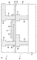
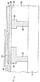
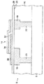
20、22 下側導電バイア
24 誘電スタック
28 銅拡散バリア層
30 ボタムプレート
32 コンデンサの誘電層
34 トッププレート
Claims (14)
- 集積回路デバイスであって、
誘電基板と、
該誘電基板内の第一と第二の導電バイアと、
それぞれ、該第一と第二の導電バイアの上に配置され、これと電気的に接触する第一と第二の導電ラナーと、
積層関係に配置されるコンデンサと、
該第一の導電バイアに電気的に接続されたボタムプレートと、
誘電層と、
該第ニの導電バイアに電気的に接続されたトッププレートと、を備えることを特徴とする集積回路デバイス。 - 集積回路デバイスであって、
誘電基板と、
該誘電基板内の第一と第二の導電バイアと、
それぞれ、該第一と第二の導電バイアの上に配置され、これと電気的に接触する第一と第二の導電ラナーと、
それぞれ、該第一と第二の導電ラナーの上に配置され、これと電気的に接続する該誘電基板内の第三と第四の導電バイアと、
積層関係に配置されるコンデンサと、
該第三の導電バイアに電気的に接続されたボタムプレートと、
誘電層と、
該第四の導電バイアと電気的に接続されたトッププレートと、を備えることを特徴とする集積回路デバイス。 - 該ボタムプレートとトッププレートの材料が、チタン、窒化チタン及び窒化タンタルの間から選択される請求項2記載の集積回路デバイス。
- 該誘電層の材料が、酸化シラン、五酸化タンタル、チタン酸ストロンチウム、チタン酸バリウム、チタン酸バリウムストロンチウム、酸化ハフニウム及び二酸化ケイ素の間から選択される請求項2記載の集積回路デバイス。
- 該第一と第二の導電バイアの導電材及び該第一と第二の導電ラナーの導電材が、銅とアルミニウムの間から選択される請求項2記載の集積回路デバイス。
- 該第一と第二の導電バイア及び該第一と第二の導電ラナーが、ジュアルダマスカス過程に従って形成される請求項2記載の集積回路デバイス。
- 該第一と第二の導電バイア及び該第一と第二の導電ラナーが、単一ダマスカス過程に従って形成される請求項2記載の集積回路デバイス。
- 集積回路デバイスであって、
半導体基板と、
積層重関係に配置されるコンデンサと、
ボタムプレートと、
誘電層と、
トッププレートであって、このプレートのエッジが該誘電層の対応するエッジと整合され、該ボタムプレートのエッジがこのプレートと該誘電層の整合されたエッジを超えて延びるトッププレートと、
該ボタムプレートの上に配置され、これと電気的に接続する第一の導電バイアと、
該トッププレートの上に配置され、これと電気的に接続する第二の導電バイアと、を備えることを特徴とする集積回路デバイス。 - 該ボタムプレートとトッププレートの材料が、チタン、窒化チタン及び窒化タンタルの間から選択される請求項8記載の集積回路デバイス。
- 該誘電層の材料が、酸化シラン、五酸化タンタル、チタン酸ストロンチウム、チタン酸バリウム、チタン酸バリウムストロンチウム、酸化ハフニウム及び二酸化ケイ素の間から選択される請求項8記載の集積回路デバイス。
- 集積回路デバイスを形成する方法であって、
半導体基板層を設けるステップと、
該半導体基板層のトップ面上にコンデンサのボタムプレートを形成するステップと、
該コンデンサのボタムプレート上にコンデンサの誘電層を形成するステップと、
該コンデンサの誘電層上にコンデンサのトッププレートを形成するステップと、
該半導体基板層上に第一の誘電基板層を形成するステップと、
該第一の誘電基板層内に第一と第二の導電バイアを形成するステップと、
それぞれ、該第一と第二の導電バイアの上に配置され、これと電気的に接触するように、該第一と第二の誘電基板層の上側領域内に第一と第二の導電ラナーを形成するステップと、
該第一の誘電基板層上に第二の誘電基板層を形成するステップと、
該第二の誘電基板層内に第三と第四の導電バイアを形成するステップと、を含み、
該第三の導電バイアが該第一の導電ラナー及び該コンデンサのボタムプレート上に配置され、これと電気的に接続し、該第四の導電バイアが該第二の導電ラナー及び該コンデンサのトッププレート上に配置され、これと電気的に接続する、ことを特徴とする方法。 - 集積回路デバイスを形成する方法であって、
半導体基板層を設けるステップと、
該半導体基板層内に第一と第二の導電バイアを形成するステップと、
該半導体基板層の上側領域内に、それぞれ、該第一と第二の導電バイアの上に配置され、これと電気的に接触する第一と第二の導電ラナーを形成するステップと、
該半導体基板層のトップ面上にコンデンサのボタムプレートを形成するステップと、
該コンデンサのボタムプレート上にコンデンサの誘電層を形成するステップと、
該コンデンサの誘電層上にコンデンサのトッププレートを形成するステップと、
基板誘電層を形成するステップと、
該基板誘電層内に第三と第四の導電バイアを形成するステップと、を含み、この第三と第四の導電バイアが、それぞれ、該第一と第二の導電ラナー及び該コンデンサのボタムプレートとトッププレート上に配置され、これと電気的に接続する、ことを特徴とする方法。 - 該コンデンサのボタムプレートを形成するステップが、更に、該半導体基板層のトップ面上の導電材層を形成するステップと、該導電材層の所定の領域を除去するステップを含む請求項12記載の方法。
- 該誘電層と該コンデンサのトッププレートを形成するステップが、更に、
該コンデンサのボタムプレートの上にコンデンサの誘電層を形成するステップと、
該コンデンサの誘電層の上にコンデンサのトッププレートを形成するステップと、
該コンデンサのトッププレートの所定の領域を除去するステップと、
該コンデンサの誘電層の所定の領域を該コンデンサのトッププレートを該除去されるべき領域を定義するマスクとして用いることで除去するステップと、を含む請求項12記載の方法。
Applications Claiming Priority (2)
| Application Number | Priority Date | Filing Date | Title |
|---|---|---|---|
| US10/260,693 US6784478B2 (en) | 2002-09-30 | 2002-09-30 | Junction capacitor structure and fabrication method therefor in a dual damascene process |
| US10/260693 | 2002-09-30 |
Publications (3)
| Publication Number | Publication Date |
|---|---|
| JP2004128498A true JP2004128498A (ja) | 2004-04-22 |
| JP2004128498A5 JP2004128498A5 (ja) | 2006-09-21 |
| JP5039267B2 JP5039267B2 (ja) | 2012-10-03 |
Family
ID=28454428
Family Applications (1)
| Application Number | Title | Priority Date | Filing Date |
|---|---|---|---|
| JP2003334485A Expired - Lifetime JP5039267B2 (ja) | 2002-09-30 | 2003-09-26 | コンデンサ構造及びこれをジュアルダマスカス過程にて製造する方法 |
Country Status (5)
| Country | Link |
|---|---|
| US (1) | US6784478B2 (ja) |
| JP (1) | JP5039267B2 (ja) |
| KR (1) | KR100988446B1 (ja) |
| GB (1) | GB2394358B (ja) |
| TW (1) | TWI273702B (ja) |
Cited By (4)
| Publication number | Priority date | Publication date | Assignee | Title |
|---|---|---|---|---|
| JP2006108490A (ja) * | 2004-10-07 | 2006-04-20 | Sony Corp | Mim型キャパシタを有する半導体デバイスおよびその製造方法 |
| JP2009049078A (ja) * | 2007-08-15 | 2009-03-05 | Elpida Memory Inc | 半導体装置の製造方法 |
| US8357991B2 (en) | 2008-11-12 | 2013-01-22 | Renesas Electronics Corporation | Semiconductor device having interconnect structure for MIM capacitor and fuse elements |
| JP2019195100A (ja) * | 2014-05-30 | 2019-11-07 | 株式会社半導体エネルギー研究所 | 半導体装置 |
Families Citing this family (24)
| Publication number | Priority date | Publication date | Assignee | Title |
|---|---|---|---|---|
| US7229875B2 (en) * | 2002-10-17 | 2007-06-12 | Samsung Electronics Co., Ltd. | Integrated circuit capacitor structure |
| KR100480641B1 (ko) * | 2002-10-17 | 2005-03-31 | 삼성전자주식회사 | 고 커패시턴스를 지니는 금속-절연체-금속 커패시터, 이를구비하는 집적회로 칩 및 이의 제조 방법 |
| US7153776B2 (en) * | 2002-11-27 | 2006-12-26 | International Business Machines Corporation | Method for reducing amine based contaminants |
| US7374993B2 (en) * | 2003-10-27 | 2008-05-20 | Micron Technology, Inc. | Methods of forming capacitors |
| US7223684B2 (en) * | 2004-07-14 | 2007-05-29 | International Business Machines Corporation | Dual damascene wiring and method |
| US7645675B2 (en) * | 2006-01-13 | 2010-01-12 | International Business Machines Corporation | Integrated parallel plate capacitors |
| US20070259519A1 (en) * | 2006-05-02 | 2007-11-08 | International Business Machines Corporation | Interconnect metallization process with 100% or greater step coverage |
| WO2008010028A1 (en) * | 2006-06-15 | 2008-01-24 | Freescale Semiconductor, Inc. | Mim capacitor integration |
| US7511939B2 (en) * | 2006-08-24 | 2009-03-31 | Analog Devices, Inc. | Layered capacitor architecture and fabrication method |
| JP2008085175A (ja) * | 2006-09-28 | 2008-04-10 | Tokyo Electron Ltd | 半導体装置の製造方法、半導体装置、基板処理システム、プログラム及び記憶媒体。 |
| US7608538B2 (en) * | 2007-01-05 | 2009-10-27 | International Business Machines Corporation | Formation of vertical devices by electroplating |
| US20100224960A1 (en) * | 2009-03-04 | 2010-09-09 | Kevin John Fischer | Embedded capacitor device and methods of fabrication |
| US9331137B1 (en) * | 2012-03-27 | 2016-05-03 | Altera Corporation | Metal-insulator-metal capacitors between metal interconnect layers |
| KR101934426B1 (ko) * | 2012-11-26 | 2019-01-03 | 삼성전자 주식회사 | 반도체 장치 및 그 제조 방법 |
| CN104103495A (zh) * | 2013-04-02 | 2014-10-15 | 中芯国际集成电路制造(上海)有限公司 | 具有mim电容的半导体器件及其形成方法 |
| US9219110B2 (en) | 2014-04-10 | 2015-12-22 | Taiwan Semiconductor Manufacturing Co., Ltd. | MIM capacitor structure |
| US9391016B2 (en) * | 2014-04-10 | 2016-07-12 | Taiwan Semiconductor Manufacturing Co., Ltd. | MIM capacitor structure |
| US9368392B2 (en) | 2014-04-10 | 2016-06-14 | Taiwan Semiconductor Manufacturing Co., Ltd. | MIM capacitor structure |
| US9425061B2 (en) | 2014-05-29 | 2016-08-23 | Taiwan Semiconductor Manufacturing Co., Ltd. | Buffer cap layer to improve MIM structure performance |
| US9478602B2 (en) * | 2014-10-07 | 2016-10-25 | Globalfoundries Inc. | Method of forming an embedded metal-insulator-metal (MIM) capacitor |
| US20170047276A1 (en) * | 2015-08-13 | 2017-02-16 | Advanced Semiconductor Engineering, Inc. | Semiconductor device package and method of manufacturing the same |
| US11121073B2 (en) * | 2018-04-02 | 2021-09-14 | Intel Corporation | Through plate interconnect for a vertical MIM capacitor |
| US11901283B2 (en) * | 2021-03-18 | 2024-02-13 | Taiwan Semiconductor Manufacturing Company, Ltd. | Capacitor and method for forming the same |
| CN115483197A (zh) * | 2021-05-31 | 2022-12-16 | 联华电子股份有限公司 | 电容器结构以及其制作方法 |
Citations (6)
| Publication number | Priority date | Publication date | Assignee | Title |
|---|---|---|---|---|
| JPH01120858A (ja) * | 1987-11-04 | 1989-05-12 | Mitsubishi Electric Corp | 集積回路装置 |
| JP2001102529A (ja) * | 1999-09-28 | 2001-04-13 | Hitachi Ltd | Mim構造の容量素子及びそれを有する半導体集積回路装置 |
| JP2001274340A (ja) * | 2000-03-28 | 2001-10-05 | Toshiba Corp | 半導体装置及びその製造方法 |
| JP2002033453A (ja) * | 2000-07-14 | 2002-01-31 | Nec Corp | 半導体装置およびその製造方法ならびに薄膜コンデンサ |
| JP2002373945A (ja) * | 2001-06-13 | 2002-12-26 | Nec Corp | 半導体装置およびその製造方法 |
| JP2003282728A (ja) * | 2002-03-21 | 2003-10-03 | Samsung Electronics Co Ltd | 半導体素子及びその製造方法 |
Family Cites Families (13)
| Publication number | Priority date | Publication date | Assignee | Title |
|---|---|---|---|---|
| JP3979711B2 (ja) * | 1997-10-17 | 2007-09-19 | 沖電気工業株式会社 | 半導体装置の製造方法 |
| US6255688B1 (en) | 1997-11-21 | 2001-07-03 | Agere Systems Guardian Corp. | Capacitor having aluminum alloy bottom plate |
| US6320244B1 (en) | 1999-01-12 | 2001-11-20 | Agere Systems Guardian Corp. | Integrated circuit device having dual damascene capacitor |
| US6271596B1 (en) | 1999-01-12 | 2001-08-07 | Agere Systems Guardian Corp. | Damascene capacitors for integrated circuits |
| US6358790B1 (en) | 1999-01-13 | 2002-03-19 | Agere Systems Guardian Corp. | Method of making a capacitor |
| TW425701B (en) | 1999-04-27 | 2001-03-11 | Taiwan Semiconductor Mfg | Manufacturing method of stack-type capacitor |
| EP1130654A1 (de) * | 2000-03-01 | 2001-09-05 | Infineon Technologies AG | Integriertes Bauelement mit Metall-Isolator-Metall-Kondensator |
| US6426249B1 (en) * | 2000-03-16 | 2002-07-30 | International Business Machines Corporation | Buried metal dual damascene plate capacitor |
| TW479310B (en) | 2000-03-31 | 2002-03-11 | Ibm | Capacitor structure and method of making same |
| US6452251B1 (en) | 2000-03-31 | 2002-09-17 | International Business Machines Corporation | Damascene metal capacitor |
| US6838717B1 (en) | 2000-08-31 | 2005-01-04 | Agere Systems Inc. | Stacked structure for parallel capacitors and method of fabrication |
| JP3746979B2 (ja) * | 2001-10-03 | 2006-02-22 | 富士通株式会社 | 半導体装置及びその製造方法 |
| US20030113974A1 (en) | 2001-12-14 | 2003-06-19 | Ning Xian J. | Stacked metal-insulator-metal capacitor structures in between interconnection layers |
-
2002
- 2002-09-30 US US10/260,693 patent/US6784478B2/en not_active Expired - Lifetime
-
2003
- 2003-08-14 GB GB0319129A patent/GB2394358B/en not_active Expired - Fee Related
- 2003-09-17 TW TW092125649A patent/TWI273702B/zh not_active IP Right Cessation
- 2003-09-26 JP JP2003334485A patent/JP5039267B2/ja not_active Expired - Lifetime
- 2003-09-30 KR KR1020030067833A patent/KR100988446B1/ko active IP Right Grant
Patent Citations (6)
| Publication number | Priority date | Publication date | Assignee | Title |
|---|---|---|---|---|
| JPH01120858A (ja) * | 1987-11-04 | 1989-05-12 | Mitsubishi Electric Corp | 集積回路装置 |
| JP2001102529A (ja) * | 1999-09-28 | 2001-04-13 | Hitachi Ltd | Mim構造の容量素子及びそれを有する半導体集積回路装置 |
| JP2001274340A (ja) * | 2000-03-28 | 2001-10-05 | Toshiba Corp | 半導体装置及びその製造方法 |
| JP2002033453A (ja) * | 2000-07-14 | 2002-01-31 | Nec Corp | 半導体装置およびその製造方法ならびに薄膜コンデンサ |
| JP2002373945A (ja) * | 2001-06-13 | 2002-12-26 | Nec Corp | 半導体装置およびその製造方法 |
| JP2003282728A (ja) * | 2002-03-21 | 2003-10-03 | Samsung Electronics Co Ltd | 半導体素子及びその製造方法 |
Cited By (4)
| Publication number | Priority date | Publication date | Assignee | Title |
|---|---|---|---|---|
| JP2006108490A (ja) * | 2004-10-07 | 2006-04-20 | Sony Corp | Mim型キャパシタを有する半導体デバイスおよびその製造方法 |
| JP2009049078A (ja) * | 2007-08-15 | 2009-03-05 | Elpida Memory Inc | 半導体装置の製造方法 |
| US8357991B2 (en) | 2008-11-12 | 2013-01-22 | Renesas Electronics Corporation | Semiconductor device having interconnect structure for MIM capacitor and fuse elements |
| JP2019195100A (ja) * | 2014-05-30 | 2019-11-07 | 株式会社半導体エネルギー研究所 | 半導体装置 |
Also Published As
| Publication number | Publication date |
|---|---|
| GB2394358A (en) | 2004-04-21 |
| TWI273702B (en) | 2007-02-11 |
| KR100988446B1 (ko) | 2010-10-18 |
| TW200405566A (en) | 2004-04-01 |
| KR20040029269A (ko) | 2004-04-06 |
| US20040061177A1 (en) | 2004-04-01 |
| GB2394358B (en) | 2006-07-19 |
| GB0319129D0 (en) | 2003-09-17 |
| JP5039267B2 (ja) | 2012-10-03 |
| US6784478B2 (en) | 2004-08-31 |
Similar Documents
| Publication | Publication Date | Title |
|---|---|---|
| JP5039267B2 (ja) | コンデンサ構造及びこれをジュアルダマスカス過程にて製造する方法 | |
| US6897505B2 (en) | On-chip capacitor | |
| US6259128B1 (en) | Metal-insulator-metal capacitor for copper damascene process and method of forming the same | |
| US6633074B2 (en) | Integrated circuit wiring with low RC time delay | |
| US6737728B1 (en) | On-chip decoupling capacitor and method of making same | |
| JP3895126B2 (ja) | 半導体装置の製造方法 | |
| US20040232552A1 (en) | Air gap dual damascene process and structure | |
| US7250334B2 (en) | Metal insulator metal (MIM) capacitor fabrication with sidewall spacers and aluminum cap (ALCAP) top electrode | |
| US8390038B2 (en) | MIM capacitor and method of making same | |
| KR20040019268A (ko) | Mim 캐패시터 및 이의 제조 방법 | |
| US9818689B1 (en) | Metal-insulator-metal capacitor and methods of fabrication | |
| US7560795B2 (en) | Semiconductor device with a capacitor | |
| JP2007221161A (ja) | 半導体デバイスで用いられるキャパシタとその製造方法 | |
| CN104576518A (zh) | 用于后段制程金属化的混合型锰和氮化锰阻障物及其制法 | |
| EP1743366B1 (en) | Wiring structure for integrated circuit with reduced intralevel capacitance | |
| KR100806034B1 (ko) | Mim 캐패시터를 가지는 반도체 소자 및 그 제조방법 | |
| KR100564626B1 (ko) | 대용량 mim 캐패시터 및 그 제조방법 | |
| US6559499B1 (en) | Process for fabricating an integrated circuit device having capacitors with a multilevel metallization | |
| JP7471305B2 (ja) | 積層された導体ライン及び空隙を有する半導体チップ | |
| CN111211092A (zh) | 半导体结构及其形成方法 | |
| US6974770B2 (en) | Self-aligned mask to reduce cell layout area | |
| KR100641983B1 (ko) | 이중 다마신 구조를 갖는 금속-절연체-금속 커패시터 및그 제조 방법 | |
| US20040018754A1 (en) | Conductive contact structure and process | |
| JP2005129816A (ja) | Mim容量素子を備えた半導体装置とその製造方法 | |
| KR20040104149A (ko) | 반도체 장치의 커패시터 구조체 및 그 제조 방법 |
Legal Events
| Date | Code | Title | Description |
|---|---|---|---|
| A521 | Request for written amendment filed |
Free format text: JAPANESE INTERMEDIATE CODE: A523 Effective date: 20060808 |
|
| A621 | Written request for application examination |
Free format text: JAPANESE INTERMEDIATE CODE: A621 Effective date: 20060808 |
|
| A977 | Report on retrieval |
Free format text: JAPANESE INTERMEDIATE CODE: A971007 Effective date: 20080926 |
|
| A131 | Notification of reasons for refusal |
Free format text: JAPANESE INTERMEDIATE CODE: A131 Effective date: 20100519 |
|
| A521 | Request for written amendment filed |
Free format text: JAPANESE INTERMEDIATE CODE: A523 Effective date: 20100819 |
|
| RD02 | Notification of acceptance of power of attorney |
Free format text: JAPANESE INTERMEDIATE CODE: A7422 Effective date: 20100819 |
|
| A131 | Notification of reasons for refusal |
Free format text: JAPANESE INTERMEDIATE CODE: A131 Effective date: 20110322 |
|
| A601 | Written request for extension of time |
Free format text: JAPANESE INTERMEDIATE CODE: A601 Effective date: 20110622 |
|
| A602 | Written permission of extension of time |
Free format text: JAPANESE INTERMEDIATE CODE: A602 Effective date: 20110627 |
|
| A521 | Request for written amendment filed |
Free format text: JAPANESE INTERMEDIATE CODE: A523 Effective date: 20110922 |
|
| A131 | Notification of reasons for refusal |
Free format text: JAPANESE INTERMEDIATE CODE: A131 Effective date: 20120319 |
|
| A521 | Request for written amendment filed |
Free format text: JAPANESE INTERMEDIATE CODE: A523 Effective date: 20120406 |
|
| A131 | Notification of reasons for refusal |
Free format text: JAPANESE INTERMEDIATE CODE: A131 Effective date: 20120509 |
|
| A521 | Request for written amendment filed |
Free format text: JAPANESE INTERMEDIATE CODE: A523 Effective date: 20120522 |
|
| TRDD | Decision of grant or rejection written | ||
| A01 | Written decision to grant a patent or to grant a registration (utility model) |
Free format text: JAPANESE INTERMEDIATE CODE: A01 Effective date: 20120611 |
|
| A01 | Written decision to grant a patent or to grant a registration (utility model) |
Free format text: JAPANESE INTERMEDIATE CODE: A01 |
|
| A61 | First payment of annual fees (during grant procedure) |
Free format text: JAPANESE INTERMEDIATE CODE: A61 Effective date: 20120709 |
|
| FPAY | Renewal fee payment (event date is renewal date of database) |
Free format text: PAYMENT UNTIL: 20150713 Year of fee payment: 3 |
|
| R150 | Certificate of patent or registration of utility model |
Free format text: JAPANESE INTERMEDIATE CODE: R150 Ref document number: 5039267 Country of ref document: JP Free format text: JAPANESE INTERMEDIATE CODE: R150 |
|
| R250 | Receipt of annual fees |
Free format text: JAPANESE INTERMEDIATE CODE: R250 |
|
| S111 | Request for change of ownership or part of ownership |
Free format text: JAPANESE INTERMEDIATE CODE: R313113 |
|
| S533 | Written request for registration of change of name |
Free format text: JAPANESE INTERMEDIATE CODE: R313533 |
|
| R350 | Written notification of registration of transfer |
Free format text: JAPANESE INTERMEDIATE CODE: R350 |
|
| R371 | Transfer withdrawn |
Free format text: JAPANESE INTERMEDIATE CODE: R371 |
|
| S111 | Request for change of ownership or part of ownership |
Free format text: JAPANESE INTERMEDIATE CODE: R313113 |
|
| R371 | Transfer withdrawn |
Free format text: JAPANESE INTERMEDIATE CODE: R371 |
|
| S111 | Request for change of ownership or part of ownership |
Free format text: JAPANESE INTERMEDIATE CODE: R313113 |
|
| R350 | Written notification of registration of transfer |
Free format text: JAPANESE INTERMEDIATE CODE: R350 |
|
| R250 | Receipt of annual fees |
Free format text: JAPANESE INTERMEDIATE CODE: R250 |
|
| R250 | Receipt of annual fees |
Free format text: JAPANESE INTERMEDIATE CODE: R250 |
|
| R250 | Receipt of annual fees |
Free format text: JAPANESE INTERMEDIATE CODE: R250 |
|
| R250 | Receipt of annual fees |
Free format text: JAPANESE INTERMEDIATE CODE: R250 |
|
| R250 | Receipt of annual fees |
Free format text: JAPANESE INTERMEDIATE CODE: R250 |
|
| R250 | Receipt of annual fees |
Free format text: JAPANESE INTERMEDIATE CODE: R250 |
|
| R250 | Receipt of annual fees |
Free format text: JAPANESE INTERMEDIATE CODE: R250 |
|
| R250 | Receipt of annual fees |
Free format text: JAPANESE INTERMEDIATE CODE: R250 |
|
| EXPY | Cancellation because of completion of term |