JP2004072120A - 現像方法及び現像装置及び液処理方法及び液処理装置 - Google Patents
現像方法及び現像装置及び液処理方法及び液処理装置 Download PDFInfo
- Publication number
- JP2004072120A JP2004072120A JP2003302071A JP2003302071A JP2004072120A JP 2004072120 A JP2004072120 A JP 2004072120A JP 2003302071 A JP2003302071 A JP 2003302071A JP 2003302071 A JP2003302071 A JP 2003302071A JP 2004072120 A JP2004072120 A JP 2004072120A
- Authority
- JP
- Japan
- Prior art keywords
- substrate
- developing
- cup
- semiconductor wafer
- processing
- Prior art date
- Legal status (The legal status is an assumption and is not a legal conclusion. Google has not performed a legal analysis and makes no representation as to the accuracy of the status listed.)
- Pending
Links
Images


Landscapes
- Photosensitive Polymer And Photoresist Processing (AREA)
- Coating Apparatus (AREA)
- Exposure Of Semiconductors, Excluding Electron Or Ion Beam Exposure (AREA)
Priority Applications (1)
| Application Number | Priority Date | Filing Date | Title |
|---|---|---|---|
| JP2003302071A JP2004072120A (ja) | 2002-07-22 | 2003-07-19 | 現像方法及び現像装置及び液処理方法及び液処理装置 |
Applications Claiming Priority (2)
| Application Number | Priority Date | Filing Date | Title |
|---|---|---|---|
| JP2002244352 | 2002-07-22 | ||
| JP2003302071A JP2004072120A (ja) | 2002-07-22 | 2003-07-19 | 現像方法及び現像装置及び液処理方法及び液処理装置 |
Related Child Applications (4)
| Application Number | Title | Priority Date | Filing Date |
|---|---|---|---|
| JP2004301203A Division JP2005109513A (ja) | 2002-07-22 | 2004-10-15 | 現像方法及び現像装置及び液処理方法及び液処理装置 |
| JP2005047256A Division JP3847767B2 (ja) | 2002-07-22 | 2005-02-23 | 基板処理方法及び基板処理装置 |
| JP2005177098A Division JP2005340845A (ja) | 2002-07-22 | 2005-06-17 | 基板処理装置及び基板処理方法並びに基板の製造方法 |
| JP2006239374A Division JP2007036268A (ja) | 2002-07-22 | 2006-09-04 | 基板処理方法及び基板処理装置 |
Publications (2)
| Publication Number | Publication Date |
|---|---|
| JP2004072120A true JP2004072120A (ja) | 2004-03-04 |
| JP2004072120A5 JP2004072120A5 (https=) | 2006-08-03 |
Family
ID=32032838
Family Applications (1)
| Application Number | Title | Priority Date | Filing Date |
|---|---|---|---|
| JP2003302071A Pending JP2004072120A (ja) | 2002-07-22 | 2003-07-19 | 現像方法及び現像装置及び液処理方法及び液処理装置 |
Country Status (1)
| Country | Link |
|---|---|
| JP (1) | JP2004072120A (https=) |
Cited By (4)
| Publication number | Priority date | Publication date | Assignee | Title |
|---|---|---|---|---|
| JP2008177436A (ja) * | 2007-01-19 | 2008-07-31 | Tokyo Electron Ltd | 現像処理装置 |
| DE102009007260B3 (de) * | 2009-02-03 | 2010-06-10 | Suss Microtec Lithography Gmbh | Vorrichtung zum Beschichten eines Substrats |
| JP2013129193A (ja) * | 2011-12-20 | 2013-07-04 | Oce Printing Systems Gmbh | 構成要素から堆積物をクリーニングする装置 |
| JP2022020735A (ja) * | 2017-08-10 | 2022-02-01 | 東京エレクトロン株式会社 | 液処理方法 |
Citations (14)
| Publication number | Priority date | Publication date | Assignee | Title |
|---|---|---|---|---|
| JPS63111960U (https=) * | 1987-01-13 | 1988-07-19 | ||
| JPH04174848A (ja) * | 1990-11-08 | 1992-06-23 | Fujitsu Ltd | レジスト塗布装置 |
| JPH0997757A (ja) * | 1995-09-28 | 1997-04-08 | Dainippon Screen Mfg Co Ltd | 基板回転式現像装置 |
| JPH09326361A (ja) * | 1996-03-05 | 1997-12-16 | Internatl Business Mach Corp <Ibm> | レジスト現像処理方法 |
| JPH10214768A (ja) * | 1997-01-29 | 1998-08-11 | Dainippon Screen Mfg Co Ltd | 基板処理装置 |
| JPH1187225A (ja) * | 1997-09-12 | 1999-03-30 | Dainippon Screen Mfg Co Ltd | 基板処理装置 |
| JP2001102298A (ja) * | 1999-07-28 | 2001-04-13 | Tokyo Electron Ltd | 現像装置、液処理装置及び現像方法 |
| JP2001104861A (ja) * | 1999-10-05 | 2001-04-17 | Tokyo Electron Ltd | 液処理装置及びその方法 |
| JP2001126982A (ja) * | 1999-08-17 | 2001-05-11 | Tokyo Electron Ltd | 液処理装置及びその方法 |
| JP3257038B2 (ja) * | 1991-06-04 | 2002-02-18 | ソニー株式会社 | 現像方法及び現像装置 |
| JP2002064044A (ja) * | 2000-08-17 | 2002-02-28 | Dainippon Screen Mfg Co Ltd | 基板処理装置および基板処理システム |
| JP2002118051A (ja) * | 2000-10-10 | 2002-04-19 | Tokyo Electron Ltd | 塗布装置及び塗布方法 |
| JP2002151376A (ja) * | 2000-11-07 | 2002-05-24 | Tokyo Electron Ltd | 現像処理方法及び現像処理装置 |
| JP2002164410A (ja) * | 2000-09-13 | 2002-06-07 | Tokyo Electron Ltd | 基板処理装置及び基板処理方法 |
-
2003
- 2003-07-19 JP JP2003302071A patent/JP2004072120A/ja active Pending
Patent Citations (14)
| Publication number | Priority date | Publication date | Assignee | Title |
|---|---|---|---|---|
| JPS63111960U (https=) * | 1987-01-13 | 1988-07-19 | ||
| JPH04174848A (ja) * | 1990-11-08 | 1992-06-23 | Fujitsu Ltd | レジスト塗布装置 |
| JP3257038B2 (ja) * | 1991-06-04 | 2002-02-18 | ソニー株式会社 | 現像方法及び現像装置 |
| JPH0997757A (ja) * | 1995-09-28 | 1997-04-08 | Dainippon Screen Mfg Co Ltd | 基板回転式現像装置 |
| JPH09326361A (ja) * | 1996-03-05 | 1997-12-16 | Internatl Business Mach Corp <Ibm> | レジスト現像処理方法 |
| JPH10214768A (ja) * | 1997-01-29 | 1998-08-11 | Dainippon Screen Mfg Co Ltd | 基板処理装置 |
| JPH1187225A (ja) * | 1997-09-12 | 1999-03-30 | Dainippon Screen Mfg Co Ltd | 基板処理装置 |
| JP2001102298A (ja) * | 1999-07-28 | 2001-04-13 | Tokyo Electron Ltd | 現像装置、液処理装置及び現像方法 |
| JP2001126982A (ja) * | 1999-08-17 | 2001-05-11 | Tokyo Electron Ltd | 液処理装置及びその方法 |
| JP2001104861A (ja) * | 1999-10-05 | 2001-04-17 | Tokyo Electron Ltd | 液処理装置及びその方法 |
| JP2002064044A (ja) * | 2000-08-17 | 2002-02-28 | Dainippon Screen Mfg Co Ltd | 基板処理装置および基板処理システム |
| JP2002164410A (ja) * | 2000-09-13 | 2002-06-07 | Tokyo Electron Ltd | 基板処理装置及び基板処理方法 |
| JP2002118051A (ja) * | 2000-10-10 | 2002-04-19 | Tokyo Electron Ltd | 塗布装置及び塗布方法 |
| JP2002151376A (ja) * | 2000-11-07 | 2002-05-24 | Tokyo Electron Ltd | 現像処理方法及び現像処理装置 |
Cited By (4)
| Publication number | Priority date | Publication date | Assignee | Title |
|---|---|---|---|---|
| JP2008177436A (ja) * | 2007-01-19 | 2008-07-31 | Tokyo Electron Ltd | 現像処理装置 |
| DE102009007260B3 (de) * | 2009-02-03 | 2010-06-10 | Suss Microtec Lithography Gmbh | Vorrichtung zum Beschichten eines Substrats |
| JP2013129193A (ja) * | 2011-12-20 | 2013-07-04 | Oce Printing Systems Gmbh | 構成要素から堆積物をクリーニングする装置 |
| JP2022020735A (ja) * | 2017-08-10 | 2022-02-01 | 東京エレクトロン株式会社 | 液処理方法 |
Similar Documents
| Publication | Publication Date | Title |
|---|---|---|
| US7338223B2 (en) | Developing method and apparatus for performing development processing properly and a solution processing method enabling enhanced uniformity in the processing | |
| TWI656570B (zh) | Substrate liquid processing device, substrate liquid processing method, and memory medium | |
| CN101114577B (zh) | 基板处理装置 | |
| JP3563605B2 (ja) | 処理装置 | |
| CN1773674B (zh) | 基板处理装置以及基板处理方法 | |
| US7722267B2 (en) | Substrate processing apparatus | |
| JP7197376B2 (ja) | 基板処理方法及び基板処理装置 | |
| US20080212049A1 (en) | Substrate processing apparatus with high throughput development units | |
| JP2012119370A (ja) | 基板処理システム、基板処理方法、プログラム及びコンピュータ記憶媒体 | |
| KR102658643B1 (ko) | 기판 처리 장치 및 그 반송 제어 방법 | |
| CN101840151A (zh) | 涂布显影装置、涂布显影方法和存储介质 | |
| JP6728358B2 (ja) | 基板処理装置、基板処理方法および記憶媒体 | |
| JP5154102B2 (ja) | 基板処理装置および基板処理方法 | |
| JP7698389B2 (ja) | 基板処理装置 | |
| JP2011205004A (ja) | 基板処理装置および基板処理方法 | |
| JP6603487B2 (ja) | 基板処理装置および基板処理方法 | |
| US7766565B2 (en) | Substrate drying apparatus, substrate cleaning apparatus and substrate processing system | |
| US20080198341A1 (en) | Substrate processing apparatus with integrated cleaning unit | |
| US20080196658A1 (en) | Substrate processing apparatus including a substrate reversing region | |
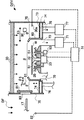
| JP2004072120A (ja) | 現像方法及び現像装置及び液処理方法及び液処理装置 | |
| JP6831889B2 (ja) | 基板処理装置および基板処理方法 | |
| JP2007036268A (ja) | 基板処理方法及び基板処理装置 | |
| JP2005109513A (ja) | 現像方法及び現像装置及び液処理方法及び液処理装置 | |
| JP2002166217A (ja) | 基板処理装置 | |
| JP2005340845A (ja) | 基板処理装置及び基板処理方法並びに基板の製造方法 |
Legal Events
| Date | Code | Title | Description |
|---|---|---|---|
| A521 | Request for written amendment filed |
Free format text: JAPANESE INTERMEDIATE CODE: A523 Effective date: 20031111 |
|
| RD02 | Notification of acceptance of power of attorney |
Free format text: JAPANESE INTERMEDIATE CODE: A7422 Effective date: 20031006 |
|
| RD02 | Notification of acceptance of power of attorney |
Free format text: JAPANESE INTERMEDIATE CODE: A7422 Effective date: 20041019 |
|
| A521 | Request for written amendment filed |
Free format text: JAPANESE INTERMEDIATE CODE: A523 Effective date: 20060620 |
|
| A621 | Written request for application examination |
Free format text: JAPANESE INTERMEDIATE CODE: A621 Effective date: 20060620 |
|
| A977 | Report on retrieval |
Free format text: JAPANESE INTERMEDIATE CODE: A971007 Effective date: 20071220 |
|
| RD04 | Notification of resignation of power of attorney |
Free format text: JAPANESE INTERMEDIATE CODE: A7424 Effective date: 20090205 |
|
| RD04 | Notification of resignation of power of attorney |
Free format text: JAPANESE INTERMEDIATE CODE: A7424 Effective date: 20090206 |
|
| A131 | Notification of reasons for refusal |
Free format text: JAPANESE INTERMEDIATE CODE: A131 Effective date: 20090303 |
|
| A521 | Request for written amendment filed |
Free format text: JAPANESE INTERMEDIATE CODE: A523 Effective date: 20090402 |
|
| RD02 | Notification of acceptance of power of attorney |
Free format text: JAPANESE INTERMEDIATE CODE: A7422 Effective date: 20090611 |
|
| RD04 | Notification of resignation of power of attorney |
Free format text: JAPANESE INTERMEDIATE CODE: A7424 Effective date: 20090824 |
|
| A131 | Notification of reasons for refusal |
Free format text: JAPANESE INTERMEDIATE CODE: A131 Effective date: 20100326 |
|
| A711 | Notification of change in applicant |
Free format text: JAPANESE INTERMEDIATE CODE: A712 Effective date: 20100510 |
|
| A02 | Decision of refusal |
Free format text: JAPANESE INTERMEDIATE CODE: A02 Effective date: 20101109 |
|
| RD04 | Notification of resignation of power of attorney |
Free format text: JAPANESE INTERMEDIATE CODE: A7424 Effective date: 20101217 |