JP2004072120A - Method and device for development, and method and device for treating liquid - Google Patents

Method and device for development, and method and device for treating liquid Download PDF

Info

Publication number
JP2004072120A
JP2004072120A JP2003302071A JP2003302071A JP2004072120A JP 2004072120 A JP2004072120 A JP 2004072120A JP 2003302071 A JP2003302071 A JP 2003302071A JP 2003302071 A JP2003302071 A JP 2003302071A JP 2004072120 A JP2004072120 A JP 2004072120A
Authority
JP
Japan
Prior art keywords
substrate
developing
cup
semiconductor wafer
processing
Prior art date
Legal status (The legal status is an assumption and is not a legal conclusion. Google has not performed a legal analysis and makes no representation as to the accuracy of the status listed.)
Pending
Application number
JP2003302071A
Other languages
Japanese (ja)
Other versions
JP2004072120A5 (en
Inventor
Yoshitake Ito
伊藤 美岳
Current Assignee (The listed assignees may be inaccurate. Google has not performed a legal analysis and makes no representation or warranty as to the accuracy of the list.)
Individual
Original Assignee
Individual
Priority date (The priority date is an assumption and is not a legal conclusion. Google has not performed a legal analysis and makes no representation as to the accuracy of the date listed.)
Filing date
Publication date
Application filed by Individual filed Critical Individual
Priority to JP2003302071A priority Critical patent/JP2004072120A/en
Publication of JP2004072120A publication Critical patent/JP2004072120A/en
Publication of JP2004072120A5 publication Critical patent/JP2004072120A5/ja
Pending legal-status Critical Current

Links

Images

Abstract

<P>PROBLEM TO BE SOLVED: To provide a method and a device for development for properly carrying out a developing treatment, and to provide a method and a device for treating the liquid for improving the uniformity of the processes by the liquid processing device. <P>SOLUTION: The device is composed so that gas discharge from a first peripheral region α of a substrate before being treated, and gas charge from a second peripheral region β between the first peripheral region and the substrate are freely possible. Therefore, it is possible to weaken the influence of airflow on the developer on the substrate, and to make the developer to be used for the developing treating act properly on an exposed resist on the substrate. <P>COPYRIGHT: (C)2004,JPO

Description

 本発明は、現像方法及び現像装置及び液処理方法及び液処理装置に関する。The present invention relates to a developing method, a developing apparatus, a liquid processing method, and a liquid processing apparatus.

 基板、例えば半導体ウエハ等の電子材料を形成する際、フォトレジストを使用したフォトリソグラフィー技術を用いることは一般的に知られている。このような技術の一例として例えば、日本の公開公報の特開平2−296316号公報がある。It is generally known to use a photolithography technique using a photoresist when forming an electronic material such as a substrate, for example, a semiconductor wafer. An example of such a technique is disclosed in Japanese Unexamined Patent Publication No. 2-296316.

     特開平2−296316号公報JP-A-2-296316

 この技術は、現像処理としてパドル現像方式を開示しており、基板の現像処理進行中は上下動自在に構成した回転ステージ上に基板を保持せずに、回転ステージと受渡し自在に構成された基板裏面に接触するゴムリングを備えたリング支持枠にて基板を支持しカバー内にて現像処理を施すものであった。This technology discloses a paddle developing method as a developing process, and does not hold the substrate on a rotatable stage configured to be movable up and down while the developing process of the substrate is in progress. The substrate was supported by a ring support frame provided with a rubber ring in contact with the back surface, and development processing was performed in the cover.

 また、他の技術の一例として例えば、日本特許の特許第3257038号がある。Also, as an example of another technique, there is Japanese Patent No. 3257038, for example.

     特許第3257038号Patent No. 3257038

 この技術は、基板の現像処理進行中は回転ステージ上に基板を保持せずに、回転ステージと受渡し自在に構成され上下動自在に構成した基板裏面と点接触するピンを備えた隔離手段にて基板を支持しカップ内にて温・湿度コントロールされたダウンフロー下で現像処理を施すものであった。This technology does not hold the substrate on the rotating stage during the development process of the substrate. The developing treatment was performed under a down flow in which the temperature and humidity were controlled in a cup while supporting the substrate.

 しかしながら、基板に現像液を供給した後に温・湿度コントロールされたダウンフローの噴出し口に基板を近接させるため、基板上の現像液がダウンフローの作用が大きくなるためにこぼれてしまう恐れがある。これにより、現像処理の歩留まりが低下してしまう要因となっていた。また、カップ内にて基板に現像液を供給し現像処理を進行し、カップ内から温・湿度コントロールされたダウンフローを排気し続けていたので、基板上の現像液に対するダウンフローの影響が多大にあり基板上の現像液がダウンフローの作用が大きくなるためにこぼれてしまう恐れがあり、現像処理の歩留まりが低下してしまう要因となっていた。However, after supplying the developing solution to the substrate, the substrate is brought close to the temperature and humidity controlled downflow outlet, and the developing solution on the substrate may be spilled due to an increased downflow effect. . As a result, the yield of the developing process is reduced. In addition, since the developing solution was supplied to the substrate in the cup to advance the developing process, and the temperature and humidity controlled downflow was continuously exhausted from the cup, the effect of the downflow on the developing solution on the substrate was great. Therefore, the developing solution on the substrate may be spilled due to an increased downflow effect, which is a factor of lowering the yield of the developing process.

 また、回転ステージ上から基板を隔離手段或いはゴムリングを備えたリング支持枠にて離間させた後、或いは回転ステージ上に基板を載置している際に基板上の現像液或いはリンス液或いは現像液・リンス液のミストが基板裏面に回りこみ隔離手段或いはゴムリングを備えたリング支持枠或いは回転ステージに付着し、それらが乾燥した際に処理室にミストとして発生したり、基板裏面にそれらが付着していたために次の処理室或いは基板搬送途中においてミストとなり処理装置全体を汚染させることとなり、これにより、現像処理の歩留まりのみならず基板処理全体としての歩留まりが低下してしまう要因となっていた。Also, after separating the substrate from the rotary stage by a separating means or a ring support frame provided with a rubber ring, or when the substrate is placed on the rotary stage, the developing solution, the rinsing solution or The mist of the liquid / rinse liquid wraps around the back surface of the substrate and adheres to a ring support frame or a rotating stage provided with an isolation means or a rubber ring, and when they dry, they are generated as mist in the processing chamber, or they are formed on the back surface of the substrate. The adhesion causes mist during the next processing chamber or during the transfer of the substrate, thereby contaminating the entire processing apparatus. This causes a reduction in not only the yield of the development processing but also the yield of the entire substrate processing. Was.

 本発明の主たる観点によれば、基板上の露光済みレジストを現像する方法であって、処理を施される前記基板の周辺の第一の周辺域から排気する工程と、前記第一の周辺域と前記基板との間の第二の周辺域から排気する工程と、を具備したことを特徴とする現像方法、が提供される。According to a main aspect of the present invention, there is provided a method of developing an exposed resist on a substrate, comprising: evacuating a first peripheral area around the substrate to be processed; and And evacuation from a second peripheral area between the substrate and the substrate.

 また、本発明の他の主たる観点によれば、基板上の露光済みレジストを現像する方法であって、前記基板の現像進行中は前記基板の周辺の第一の周辺域から排気する工程と、前記第一の周辺域と前記基板との間の第二の周辺域から排気及び第一の周辺域から排気する工程と、を具備したことを特徴とする現像方法、が提供される。According to another main aspect of the present invention, there is provided a method of developing an exposed resist on a substrate, wherein the step of evacuating a first peripheral area around the substrate during development of the substrate includes: Exhausting from a second peripheral area and exhausting from the first peripheral area between the first peripheral area and the substrate.

 また、本発明の他の主たる観点によれば、基板上の露光済みレジストを現像する方法であって、前記基板を支持した状態で現像処理工程を行う際は前記基板の周辺の第一の周辺域から排気する工程と、前記基板を真空吸着にて保持した状態でリンス工程を行う際は前記第一の周辺域と前記基板との間の第二の周辺域から排気する工程と、を具備したことを特徴とする現像方法、が提供される。According to another main aspect of the present invention, there is provided a method of developing an exposed resist on a substrate, wherein a developing process is performed in a state in which the substrate is supported, and a first peripheral portion around the substrate is used. Exhausting from a region, and exhausting from a second peripheral region between the first peripheral region and the substrate when performing a rinsing process while holding the substrate by vacuum suction. And a developing method characterized by the following.

 また、本発明の他の主たる観点によれば、処理室内で基板上の露光済みレジストを現像する方法であって、前記基板の裏面側を真空吸着により保持し前記基板に対して現像液を供給する第一の工程と、前記基板の裏面側を支持し現像処理を進行させる第二の工程と、を具備し、前記第一と第二の工程において前記処理室内の気流の流れを変化せしめることを特徴とする現像方法、が提供される。According to another main aspect of the present invention, there is provided a method of developing an exposed resist on a substrate in a processing chamber, the method including supplying a developing solution to the substrate while holding the back surface of the substrate by vacuum suction. A first step of performing, and a second step of supporting the back surface side of the substrate and performing a development process, wherein the flow of the airflow in the processing chamber is changed in the first and second steps. The development method characterized by the above.

 また、本発明の他の主たる観点によれば、処理室内で基板上の露光済みレジストを現像する方法であって、前記基板の裏面側を支持し前記基板に対して現像液を供給する第一の工程と、前記基板裏面側を支持し現像処理を進行させる第二の工程と、前記基板の裏面側を真空吸着により保持し前記基板に対してリンス液を供給する第三の工程と、を具備し、前記第一の工程又は/及び第三の工程と第二の工程とにおいて前記処理室内の気流の流れを変化せしめることを特徴とする現像方法、が提供される。According to another main aspect of the present invention, there is provided a method of developing an exposed resist on a substrate in a processing chamber, the method comprising: supporting a back side of the substrate and supplying a developing solution to the substrate. And a second step of supporting the substrate back side and proceeding with the development process, and a third step of holding the back side of the substrate by vacuum suction and supplying a rinsing liquid to the substrate, A developing method, wherein a flow of an airflow in the processing chamber is changed in the first step and / or the third step and the second step.

 また、本発明の他の主たる観点によれば、処理室内で基板上の露光済みレジストを現像する方法であって、前記基板の裏面側を真空吸着により保持し前記基板に対して現像液を供給した後、基板上の現像液濃度を変化せしめる第一の工程と、前記基板裏面側を支持し現像処理を進行させる第二の工程と、を具備し、前記第一と第二の工程において前記処理室内の気流の流れを変化せしめることを特徴とする現像方法、が提供される。According to another main aspect of the present invention, there is provided a method of developing an exposed resist on a substrate in a processing chamber, the method including supplying a developing solution to the substrate while holding the back surface of the substrate by vacuum suction. After that, a first step of changing the concentration of the developer on the substrate, and a second step of supporting the substrate back side and proceeding with the development process, comprising, in the first and second steps, There is provided a developing method characterized by changing a flow of an airflow in a processing chamber.

 上記のような構成によれば、主に、基板上の現像液に対する気流の影響を低減することができるので、現像処理に施す現像液を適切に基板上の露光済みレジストに作用させることができ、歩留まりを向上することができる。According to the above configuration, mainly, the influence of the airflow on the developing solution on the substrate can be reduced, so that the developing solution applied to the developing process can appropriately act on the exposed resist on the substrate. , The yield can be improved.

 また、本発明の他の主たる観点によれば、カップ内で基板上の露光済みレジストを現像する方法であって、前記基板の裏面側を支持或いは保持し前記基板及びカップに対して同時に現像液を供給する工程を具備したことを特徴とする現像方法、が提供される。According to another main aspect of the present invention, there is provided a method for developing an exposed resist on a substrate in a cup, comprising: A developing method, comprising the step of:

 また、本発明の他の主たる観点によれば、カップ内で基板上の露光済みレジストを現像する方法であって、前記基板の裏面側を支持或いは保持し前記基板及びカップに対して同時に現像液を供給する工程と、前記基板上の現像液の濃度を変化させる工程を具備したことを特徴とする現像方法、が提供される。According to another main aspect of the present invention, there is provided a method for developing an exposed resist on a substrate in a cup, comprising: And a step of changing the concentration of the developer on the substrate.

 上記のような構成によれば、主に、基板及びカップに対して同時に現像液を供給しているので、適量の現像液を基板上に盛ることができるとともに不要な現像液をカップを介して除去できるので基板の処理における現像液の作用のバラツキを抑制できるので基板の歩留まりを向上することができる。According to the above configuration, mainly, the developing solution is supplied to the substrate and the cup at the same time, so that an appropriate amount of the developing solution can be poured on the substrate and unnecessary developing solution is supplied through the cup. Since the removal can be suppressed, the variation in the action of the developing solution in the processing of the substrate can be suppressed, and the yield of the substrate can be improved.

 また、本発明の他の主たる観点によれば、カップ内で基板上の露光済みレジストを現像する方法であって、前記カップ内の第一の領域で基板を囲い現像液を供給する工程と、前記カップ内の前記第一の領域より狭い第二の領域で基板を囲いリンス液を供給する工程と、を具備したことを特徴とする現像方法が提供される。According to another main aspect of the present invention, there is provided a method of developing an exposed resist on a substrate in a cup, wherein a step of supplying a developer around the substrate in a first region in the cup, Supplying a rinsing liquid surrounding the substrate in a second area smaller than the first area in the cup.

 また、本発明の他の主たる観点によれば、カップ内で基板上の露光済みレジストを現像する方法であって、前記カップ外の領域を排気しつつ前記基板の裏面側を支持し前記基板及びカップに対して現像液を供給する工程と、前記カップ内の領域と前記カップ外の領域を同時に排気しつつ前記基板の裏面側を保持し前記基板にリンス液を供給する工程と、を具備したことを特徴とする現像方法、が提供される。According to another main aspect of the present invention, there is provided a method of developing an exposed resist on a substrate in a cup, wherein the substrate is supported while supporting a rear surface side of the substrate while exhausting an area outside the cup. Supplying a developing solution to the cup; and supplying a rinsing liquid to the substrate while holding the back side of the substrate while simultaneously evacuating an area inside the cup and an area outside the cup. A developing method is provided.

 上記のような構成によれば、主に、基板上の現像液に対する気流の影響を低減することができるので、現像処理に施す現像液を適切に基板上の露光済みレジストに作用させることができ、歩留まりを向上することができる。According to the above configuration, mainly, the influence of the airflow on the developing solution on the substrate can be reduced, so that the developing solution applied to the developing process can appropriately act on the exposed resist on the substrate. , The yield can be improved.

 また、本発明の他の主たる観点によれば、カップ内で基板上の露光済みレジストを現像する方法であって、前記基板の裏面側を支持する工程と、前記基板の裏面側を真空吸着により保持した後で再度前記基板の裏面側を支持し前記基板に対して現像液を供給する工程と、を具備したことを特徴とする現像方法、が提供される。According to another main aspect of the present invention, there is provided a method of developing an exposed resist on a substrate in a cup, wherein the step of supporting the back side of the substrate and the back side of the substrate by vacuum suction. And holding the back surface side of the substrate again and supplying a developing solution to the substrate after the holding, thereby providing a developing method.

 このような構成によれば、主に、基板の受渡しを確実に行うことができ、現像処理に施す現像液を適切に基板上の露光済みレジストに作用させることができ、歩留まりを向上することができる。According to such a configuration, mainly, the transfer of the substrate can be reliably performed, and the developing solution to be applied to the developing process can be appropriately applied to the exposed resist on the substrate, and the yield can be improved. it can.

 また、本発明の他の主たる観点によれば、基板上の露光済みレジストを現像する装置であって、前記基板の周囲に配置される第一の囲い体と、この第一の囲い体の周囲に配置される第二の囲い体と、この第二の囲い体と前記第一の囲い体との間の領域及び前記第一の囲い体内の領域を各々独立して及び/又は同時に排気自在に構成された排気機構と、を具備したことを特徴とする現像装置、が提供される。According to another main aspect of the present invention, there is provided an apparatus for developing an exposed resist on a substrate, comprising: a first enclosure disposed around the substrate; and a periphery of the first enclosure. And a region between the second enclosure and the first enclosure and a region in the first enclosure can be independently and / or simultaneously evacuated. And a configured exhaust mechanism.

 上記のような構成によれば、主に、基板上の現像液に対する気流の影響を低減することができるので、現像処理に施す現像液を適切に基板上の露光済みレジストに作用させることができ、歩留まりを向上することができる。According to the above configuration, mainly, the influence of the airflow on the developing solution on the substrate can be reduced, so that the developing solution applied to the developing process can appropriately act on the exposed resist on the substrate. , The yield can be improved.

 また、本発明の他の主たる観点によれば、基板上の露光済みレジストを現像する装置であって、前記基板の周囲に配置される第一の囲い体と、この第一の囲い体の周囲に配置される第二の囲い体と、前記第一の囲い体内に配置され前記基板を支持する支持機構と、前記第一の囲い体内に配置され前記基板を真空吸着により保持する保持機構と、前記支持機構で前記基板が支持されている際は前記第一の囲い体と前記第二の囲い体との間の領域から排気する排気機構と、を具備したことを特徴とする現像装置、が提供される。According to another main aspect of the present invention, there is provided an apparatus for developing an exposed resist on a substrate, comprising: a first enclosure disposed around the substrate; and a periphery of the first enclosure. A second enclosure disposed on the, a support mechanism disposed in the first enclosure and supporting the substrate, a holding mechanism disposed in the first enclosure and holding the substrate by vacuum suction, A developing device, comprising: an exhaust mechanism that exhausts air from an area between the first enclosure and the second enclosure when the substrate is supported by the support mechanism. Provided.

 上記のような構成によれば、主に、基板の受渡しを確実に行うことができ、さらに基板上の現像液に対する気流の影響を低減することができるので、現像処理に施す現像液を適切に基板上の露光済みレジストに作用させることができ、歩留まりを向上することができる。According to the above configuration, mainly, the transfer of the substrate can be reliably performed, and the influence of the airflow on the developer on the substrate can be reduced. It can act on the exposed resist on the substrate, and the yield can be improved.

 また、本発明の他の主たる観点によれば、カップ内で基板上の露光済みレジストを現像する装置であって、前記基板の裏面側を支持或いは保持し前記基板及びカップに対して現像液を供給する現像液供給機構を具備したことを特徴とする現像装置、が提供される。According to another main aspect of the present invention, there is provided an apparatus for developing an exposed resist on a substrate in a cup, wherein a developing solution is supported or held on a back side of the substrate and a developing solution is applied to the substrate and the cup. A developing device comprising a developing solution supply mechanism for supplying the developing solution.

 このような構成によれば、主に、基板及びカップに対して現像液を供給しているので、適量の現像液を基板上に盛ることができるとともに不要な現像液をカップを介して除去できるので基板の処理における現像液の作用のバラツキを抑制できるので基板の歩留まりを向上することができる。According to such a configuration, since the developing solution is mainly supplied to the substrate and the cup, an appropriate amount of the developing solution can be poured on the substrate and unnecessary developing solution can be removed through the cup. Therefore, the variation in the action of the developing solution in the processing of the substrate can be suppressed, and the yield of the substrate can be improved.

 また、本発明の他の主たる観点によれば、基板上の露光済みレジストを現像する装置であって、前記基板の裏面側に配置され現像液が前記基板裏面の中心部に進入するのを防止する液進入防止機構と、この液進入防止機構に設けられ前記基板を支持する支持機構と、を具備したことを特徴とする現像装置、が提供される。According to another main aspect of the present invention, there is provided an apparatus for developing an exposed resist on a substrate, wherein the apparatus is disposed on a back surface side of the substrate and prevents a developing solution from entering a central portion of the back surface of the substrate. And a support mechanism provided on the liquid intrusion prevention mechanism for supporting the substrate.

 また、本発明の他の主たる観点によれば、基板上の露光済みレジストを現像する装置であって、前記基板の裏面側に配置され現像液が前記基板裏面の中心部に進入するのを防止する防止部を備えた液進入防止機構と、この液進入防止機構の前記防止部より前記基板の中心部方向に設けられ前記基板を支持する複数の支持機構と、を具備したことを特徴とする現像装置、が提供される。According to another main aspect of the present invention, there is provided an apparatus for developing an exposed resist on a substrate, wherein the apparatus is disposed on a back surface side of the substrate and prevents a developing solution from entering a central portion of the back surface of the substrate. And a plurality of support mechanisms provided in the direction of the center of the substrate from the prevention portion of the liquid intrusion prevention mechanism to support the substrate. A developing device is provided.

 また、本発明の他の主たる観点によれば、カップ内にて基板上の露光済みレジストを現像する装置であって、前記基板の裏面側に配置され現像液が前記基板裏面の中心部に進入するのを防止する防止部を備えた液進入防止機構と、この液進入防止機構の前記防止部より前記基板の中心部方向に設けられ前記基板を支持する複数の支持機構と、この支持機構により前記基板が支持され現像処理進行中は前記カップ内からの排気を停止する制御機構と、を具備したことを特徴とする現像装置、が提供される。According to another main aspect of the present invention, there is provided an apparatus for developing an exposed resist on a substrate in a cup, wherein the developing solution is disposed on a back side of the substrate and enters a central portion of the back side of the substrate. A liquid intrusion prevention mechanism having a prevention part for preventing the liquid penetration prevention mechanism, a plurality of support mechanisms provided in the direction of the center of the substrate from the prevention part of the liquid intrusion prevention mechanism to support the substrate, and the support mechanism A control mechanism for supporting the substrate and stopping exhaust from the inside of the cup while the developing process is in progress.

 また、本発明の他の主たる観点によれば、基板上の露光済みレジストを現像する装置であって、前記基板の周囲に配置される第一の囲い体と、この第一の囲い体の周囲に配置される第二の囲い体と、前記第一の囲い体内に配置され前記基板を真空吸着により保持する保持機構と、前記第一の囲い体内に配置され且つ前記基板の裏面側に配置され現像液が前記基板裏面の中心部に進入するのを防止する液進入防止機構と、この液進入防止機構に設けられ前記基板を支持する複数の支持機構と、前記第二の囲い体と前記第一の囲い体との間の領域及び前記第一の囲い体内の領域を同時或いは選択的に排気自在に構成された排気機構と、を具備したことを特徴とする現像装置、が提供される。According to another main aspect of the present invention, there is provided an apparatus for developing an exposed resist on a substrate, comprising: a first enclosure disposed around the substrate; and a periphery of the first enclosure. A second enclosure disposed in the first enclosure, a holding mechanism disposed in the first enclosure for holding the substrate by vacuum suction, and disposed in the first enclosure and disposed on the back side of the substrate. A liquid intrusion prevention mechanism for preventing the developer from entering the center of the back surface of the substrate, a plurality of support mechanisms provided in the liquid intrusion prevention mechanism to support the substrate, the second enclosure and the second A developing device, comprising: an exhaust mechanism configured to simultaneously or selectively exhaust an area between the first enclosure and an area in the first enclosure.

 上記のような構成によれば、保持機構及び支持機構に現像液或いはリンス液等の付着を抑制することができ、それらが乾燥した際にミストとして発生するのを抑制することができる。もって、基板の歩留まりを向上することができる。According to the above configuration, it is possible to suppress the adhesion of the developing solution or the rinsing liquid to the holding mechanism and the supporting mechanism, and to suppress the generation of mist when they are dried. Thus, the yield of the substrate can be improved.

 また、本発明の他の主たる観点によれば、基板に処理液を供給して処理を施す方法であって、前記基板の周辺の第一の周辺域から排気する工程と、前記第一の周辺域と前記基板との間の第二の周辺域から排気及び第一の周辺域から排気する工程と、を具備したことを特徴とする液処理方法、が提供される。According to another main aspect of the present invention, there is provided a method of supplying a processing liquid to a substrate to perform processing, wherein the step of evacuating the substrate from a first peripheral area around the substrate includes: Exhausting from a second peripheral area and exhausting from the first peripheral area between the area and the substrate.

 また、本発明の他の主たる観点によれば、温・湿度コントロールされた気体が供給される処理室内に配置されたカップ内で基板に処理液を供給して処理を施す方法であって、前記温・湿度コントロールされた気体の供給を停止せずに前記基板の処理中は前記カップ内からの排気を低下又は停止し、前記カップ外から前記気体を排気することを特徴とする液処理方法、が提供される。According to another main aspect of the present invention, there is provided a method of performing processing by supplying a processing liquid to a substrate in a cup disposed in a processing chamber to which a temperature- and humidity-controlled gas is supplied, A liquid processing method, characterized in that, during the processing of the substrate, the exhaust from the inside of the cup is reduced or stopped during the processing of the substrate without stopping the supply of the temperature and humidity controlled gas, and the gas is exhausted from outside the cup. Is provided.

 また、本発明の他の主たる観点によれば、処理室内に配置されたカップ内で基板に処理液を供給して処理を施す装置であって、前記カップの上下動の動作と連動し前記処理室内の気流の流れを変化せしめる気流変動機構を具備したことを特徴とする液処理装置、が提供される。According to another main aspect of the present invention, there is provided an apparatus for performing processing by supplying a processing liquid to a substrate in a cup disposed in a processing chamber, wherein the processing is performed in conjunction with a vertical movement of the cup. There is provided a liquid processing apparatus including an airflow fluctuation mechanism for changing a flow of an airflow in a room.

 上記のような構成によれば、主に、基板上の処理液に対する気流の影響を低減することができるので、歩留まりを向上することができる。According to the configuration described above, mainly, the influence of the air flow on the processing liquid on the substrate can be reduced, so that the yield can be improved.

 本発明は、主に処理を施される前記基板の周辺の第一の周辺域から排気、さらに、第一の周辺域と基板との間の第二の周辺域から排気自在に構成されているので、基板上の現像液に対する気流の影響を低減することができ、現像処理に施す現像液を適切に基板上の露光済みレジストに作用させることができるので、基板の処理の均一性を向上し、もって基板の処理に係る歩留まりを向上することができるという効果を奏する。The present invention is configured such that exhaust can be performed from a first peripheral area around the substrate to be mainly processed, and further, can be freely exhausted from a second peripheral area between the first peripheral area and the substrate. Therefore, it is possible to reduce the influence of the air flow on the developing solution on the substrate, and to allow the developing solution to be applied to the developing process to properly act on the exposed resist on the substrate, thereby improving the uniformity of the processing of the substrate. Accordingly, the effect of improving the yield related to the processing of the substrate can be obtained.

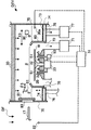
 以下、本発明の実施の形態について図面を参照しながら詳細に説明をおこなう。 図1は、液処理装置、例えばレジスト処理装置としての塗布・現像装置の実施の形態における全体構造を示す概略平面図である。Hereinafter, embodiments of the present invention will be described in detail with reference to the drawings. FIG. 1 is a schematic plan view showing the overall structure of a liquid processing apparatus, for example, a coating and developing apparatus as a resist processing apparatus according to an embodiment.

 このレジスト処理装置1は、基板、例えば半導体ウエハWを複数枚収納自在のカセットCを複数載置自在に構成されたカセット載置部U1とこのカセット載置部U1のカセットCに対して半導体ウエハWを一枚毎搬入出自在に構成された基板搬出入機構2を配置する基板搬入出機構部U2で構成されたカセットユニット部CUと、他の装置、例えば半導体ウエハWに対して露光処理を施す露光装置3に対して半導体ウエハWを一枚毎渡す渡し部4と露光装置3から半導体ウエハWを一枚毎受け取る受取部5と半導体ウエハWを一枚毎搬入出自在に構成された基板搬出入機構6とで構成されたインターフェイスユニット部IFUと、半導体ウエハWに対して所定の処理を施す処理部、例えば液処理部としてレジスト液を塗布する塗布処理部COTと半導体ウエハW上の露光済みレジストを現像する現像処理部DEVと半導体ウエハWに対して所定のタイミングで半導体ウエハW上のレジスト膜の状態を検査する検査処理部7と前記基板搬出入機構2,6との間で半導体ウエハWを一枚毎搬入出自在に構成された基板受渡部8,9とこれら基板受渡部8,9と塗布処理部COT・現像処理部DEV・検査処理部7に対して半導体ウエハWを一枚毎搬送自在に構成された基板搬送機構10とで構成されたプロセスユニット部PUと、で主要部が構成されている。The resist processing apparatus 1 includes a cassette mounting unit U1 configured to mount a plurality of cassettes C capable of accommodating a plurality of substrates, for example, semiconductor wafers W, and a semiconductor wafer with respect to the cassette C of the cassette mounting unit U1. Exposure processing is performed on a cassette unit CU including a substrate loading / unloading mechanism unit U2 in which a substrate loading / unloading mechanism 2 configured to freely load / unload W wafers and another apparatus, for example, a semiconductor wafer W. A transfer unit 4 for transferring the semiconductor wafers W one by one to the exposure apparatus 3 to be applied, a receiving unit 5 for receiving the semiconductor wafers W one by one from the exposure apparatus 3, and a substrate configured to be able to carry in and out the semiconductor wafers W one by one An interface unit IFU constituted by the carry-in / carry-out mechanism 6, and a processing unit for performing predetermined processing on the semiconductor wafer W, for example, a coating processing unit C for applying a resist liquid as a liquid processing unit T, a development processing unit DEV for developing the exposed resist on the semiconductor wafer W, an inspection processing unit 7 for inspecting the state of the resist film on the semiconductor wafer W at a predetermined timing, and the substrate loading / unloading mechanism. Substrate transfer units 8 and 9 configured so that semiconductor wafers W can be carried in and out one by one between the substrates 2 and 6, these substrate transfer units 8 and 9, a coating processing unit COT, a development processing unit DEV, and an inspection processing unit 7. The main part is composed of a process unit PU composed of a substrate transport mechanism 10 configured to be capable of transporting semiconductor wafers W one by one.

 なお、前述の基板搬出入機構2,6の半導体ウエハWを真空吸着にて保持或いは半導体ウエハWの周縁部を点接触或いは線接触にて支持するアーム11,12は、図中の垂直方向Z1,2と進退方向Y1,2方向と回転方向θ1,2に移動自在に構成され、アーム11,12の基台13,14はアーム11,12ごと図中水平方向X1,2に移動自在に構成されている。また、プロセスユニット部PUの基板搬送機構10のアーム17は、半導体ウエハWの周縁部を点接触或いは線接触にて支持するように構成され、図中の垂直方向Z0と進退方向Y0方向と回転方向θ0に移動自在に構成されている。なお、便宜上、基板搬出入機構2,6及び基板搬送機構10を上述のように構成したが、多関節ロボットを使用しても良いことは言うまでもなく、基板搬入出機構部U2及びインターフェイスユニット部IFUには、上記機能が達成できる搬送機構が配置されるよう構成されていれば良い。The arms 11 and 12 for holding the semiconductor wafer W of the above-described substrate loading / unloading mechanisms 2 and 6 by vacuum suction or supporting the peripheral portion of the semiconductor wafer W by point contact or line contact are provided in the vertical direction Z1 in the drawing. , 2 and the reciprocating directions Y1, 2 and the rotating directions θ1, 2. The bases 13, 14 of the arms 11, 12 are configured to be movable in the horizontal directions X1, X2 in the figure together with the arms 11, 12. Have been. Further, the arm 17 of the substrate transfer mechanism 10 of the process unit PU is configured to support the periphery of the semiconductor wafer W by point contact or line contact, and rotates in the vertical direction Z0 and the reciprocating direction Y0 in the drawing. It is configured to be movable in the direction θ0. For convenience, the substrate loading / unloading mechanisms 2 and 6 and the substrate transporting mechanism 10 are configured as described above, but it goes without saying that an articulated robot may be used, and the substrate loading / unloading mechanism U2 and the interface unit IFU. , A transport mechanism capable of achieving the above function may be provided.

 また、基板受渡部8,9の各々下方位置には半導体ウエハWに対して、処理室内と略同温の温度に温調する図示しない温調処理部が複数積層して配置されており、さらに、これら複数の温調処理部の下方位置には半導体ウエハWに対して、処理ガス、例えばHMDSガスを用いた処理を施す図示しないガス処理部が複数積層して配置されており、さらに、基板受渡部8,9の各々上方位置には半導体ウエハWに対して、所定の室温以上の温度にて加熱して処理を施す図示しない加熱処理部が複数積層して配置され、熱処理部が構成されている。Further, a plurality of temperature control processing units (not shown) for controlling the temperature of the semiconductor wafer W to substantially the same temperature as the inside of the processing chamber with respect to the semiconductor wafer W are disposed below the substrate transfer units 8 and 9, respectively. A plurality of gas processing units (not shown) for performing processing using a processing gas, for example, HMDS gas, on the semiconductor wafer W are disposed below the plurality of temperature control processing units. Above each of the transfer units 8 and 9, a plurality of heat treatment units (not shown) for heating and processing the semiconductor wafer W at a temperature equal to or higher than a predetermined room temperature are stacked and arranged to form a heat treatment unit. ing.

 また、プロセスユニット部PUの検査処理部7に対して、プロセスユニット部PUの基板搬送機構10とカセットユニット部CUの基板搬出入機構2は、半導体ウエハWを各々搬入出自在に構成されており、処理前の半導体ウエハW、上述した各処理部及び/または露光装置で処理した処理後の半導体ウエハWに対して検査、例えば半導体ウエハW上のレジスト膜の膜厚等を検査自在に構成されている。Further, the substrate transfer mechanism 10 of the process unit PU and the substrate loading / unloading mechanism 2 of the cassette unit CU are configured to be capable of loading / unloading the semiconductor wafer W with respect to the inspection processing unit 7 of the process unit PU. The semiconductor wafer W before processing, the semiconductor wafer W after processing in each of the above-described processing units and / or the exposure apparatus can be inspected, for example, the thickness of a resist film on the semiconductor wafer W can be inspected. ing.

 また、カセットユニット部CUの基板搬入出機構部U2とプロセスユニット部PUとインターフェイスユニット部IFUの上部には各々図示しないフィルタ部が設けられており、それらのフィルタ部からはそれぞれのユニット内に温度・湿度が所定の値に設定された温度・湿度エアーを供給するよう構成され、さらにそれぞれのユニットの下部に設けられた排気口より前記温度・湿度エアーを所定量に各々排気設定機構により設定し回収自在に構成されて各ユニットに温度・湿度エアーのダウンフローが形成されるよう構成されている。Further, filter units (not shown) are provided above the substrate loading / unloading mechanism unit U2, the process unit unit PU, and the interface unit unit IFU of the cassette unit unit CU, respectively.・ Humidity is configured to supply temperature / humidity air set to a predetermined value, and the temperature / humidity air is set to a predetermined amount by an exhaust setting mechanism from an exhaust port provided at the lower part of each unit. It is configured so that it can be collected freely, and a downflow of temperature / humidity air is formed in each unit.

 さらに、カセットユニット部CUの基板搬入出機構部U2とプロセスユニット部PUとインターフェイスユニット部IFUの各々の排気設定機構によりそれぞれのユニット部の圧力は、カセットユニット部CUの基板搬入出機構部U2よりプロセスユニット部PUのほうが圧力が高く設定されており、さらにインターフェイスユニット部IFUよりプロセスユニット部PUのほうが圧力が高く設定されており、さらに、インターフェイスユニット部IFUより露光装置3内の方が圧力が高く設定されるよう構成されており、プロセスユニット部PU内或いは露光装置3内に不要なミストが入り込み半導体ウエハWの処理に悪影響が起こる要因となるのを抑制するようにされている。また、カセットユニット部CUの雰囲気中に含まれる酸素及び/または酸性ガス(NOX,SOX,HS,COなど)及び/または塩基性ガス(アンモニア、アミンなど)及び/または湿度の量に比べ、プロセスユニット部PU及び/またはインターフェイスユニット部IFUの雰囲気中に含有する量は実質的に少なく設定されている。これは、特に露光前或いは露光後の処理において、それらの影響を軽減することにより半導体ウエハWの処理の歩留まりを向上するためである。Further, the pressure of each unit is set by the substrate loading / unloading mechanism U2 of the cassette unit CU by the exhaust setting mechanism of the substrate loading / unloading mechanism U2, the process unit PU, and the interface unit IFU of the cassette unit CU. The process unit PU is set to have a higher pressure, the process unit PU is set to have a higher pressure than the interface unit IFU, and the pressure inside the exposure apparatus 3 is set higher than the interface unit IFU. It is configured to be set to a high value, so as to prevent unnecessary mist from entering the process unit unit PU or the exposure apparatus 3 and causing a bad influence on the processing of the semiconductor wafer W. Further, the amount of oxygen and / or acid gas (NOX, SOX, H 2 S, CO 2 and the like) and / or basic gas (ammonia, amine and the like) and / or humidity contained in the atmosphere of the cassette unit CU may be reduced. In comparison, the amount contained in the atmosphere of the process unit PU and / or the interface unit IFU is set substantially smaller. This is to improve the yield of the processing of the semiconductor wafer W by reducing the influence thereof particularly in the processing before or after the exposure.

 なお、上述のようにカセットユニット部CUの基板搬入出機構部U2とプロセスユニット部PU間或いはプロセスユニット部PUとインターフェイスユニット部IFU間の雰囲気を遮断するようにそれぞれの間には壁20が設けられ、基板受渡部8,9と検査処理部7の基板搬入出口19は半導体ウエハWの搬入出の工程以外はその基板搬入出口19を図示しない開閉機構、例えば蓋にて開閉自在に構成されて、カセットユニット部CUの基板搬入出機構部U2とプロセスユニット部PUとインターフェイスユニット部IFUの各々の雰囲気を遮断するよう構成されている。As described above, the wall 20 is provided between the substrate carrying-in / out mechanism U2 of the cassette unit CU and the process unit PU or between the process unit PU and the interface unit IFU so as to shut off the atmosphere. The substrate transfer ports 8, 9 and the substrate loading / unloading port 19 of the inspection processing section 7 are configured such that the substrate loading / unloading port 19 can be opened and closed by a not-shown opening / closing mechanism, for example, a lid except for the step of loading / unloading the semiconductor wafer W. The atmosphere of each of the substrate loading / unloading mechanism U2, the process unit PU, and the interface unit IFU of the cassette unit CU is configured to be shut off.

 また、プロセスユニット部PUの塗布処理部COTは複数積層して配置されており、さらに現像処理部DEVも同様に複数積層して配置されている。これらの処理部に対しても基板搬送機構10により半導体ウエハWは搬入出自在に構成されている。なお、塗布処理部COT及び/または現像処理部DEVは、後述するように各々、温度・湿度が所定の値に設定されており、それらの処理部内の圧力は、それらの処理部内の排気状態が変化したとしても、プロセスユニット部PU内より高く設定されている。これは、液処理部である塗布処理部COT内及び現像処理部DEV内に不要なミストが入り込み半導体ウエハWの処理に悪影響が起こる要因となるのを抑制するためである。また、塗布処理部COT及び/または現像処理部DEV内の雰囲気は、プロセスユニット部PU内の雰囲気に比べ、その雰囲気内に含まれる酸素及び/または酸性ガス(NOX,SOX,HS,COなど)及び/または塩基性ガス(アンモニア、アミンなど)及び/または湿度の量が低くなるよう設定されている。これにより、それらの影響を軽減することにより半導体ウエハWの処理の歩留まりを向上するためである。Further, a plurality of coating processing sections COT of the process unit section PU are arranged in a stacked manner, and a plurality of development processing sections DEV are similarly arranged in a stacked manner. The semiconductor wafer W is also configured to be able to carry in and out of these processing units by the substrate carrying mechanism 10. Note that the temperature and humidity of the coating processing unit COT and / or the development processing unit DEV are set to predetermined values, respectively, as described later. The pressure in these processing units depends on the exhaust state in those processing units. Even if it changes, it is set higher than in the process unit PU. This is to prevent unnecessary mist from entering the coating processing unit COT and the developing processing unit DEV, which are liquid processing units, to cause a factor that adversely affects the processing of the semiconductor wafer W. Further, the atmosphere in the coating section COT and / or the development section DEV is compared with the atmosphere in the process unit PU, and the oxygen and / or acid gas (NOX, SOX, H 2 S, CO 2 ) and / or basic gas (ammonia, amine, etc.) and / or humidity. This is to reduce the influence thereof and improve the yield of processing the semiconductor wafer W.

 つぎに、現像処理部DEVの構成について、図2,図3,図4に基づいて説明する。
 この現像処理部DEVは、上部に処理室内に所定の値に設定された温度・湿度がコントロールされたエアーを供給するエアー供給機構30が設けられており、処理室内に設けられたセンサー30aの検出データに基づき制御機構31により、所定の温度及び湿度に維持されるよう構成されている。
Next, the configuration of the developing unit DEV will be described with reference to FIGS.
The development processing unit DEV is provided with an air supply mechanism 30 for supplying air of which temperature and humidity are set to predetermined values in a processing chamber at an upper portion thereof, and a detection unit 30a provided in the processing chamber detects the air. The control mechanism 31 is configured to maintain predetermined temperature and humidity based on the data.

 また、処理室の下方位置には、半導体ウエハWの裏面を真空吸着して保持する保持機構としてのチャック32が配置され、このチャック32は回転駆動機構、例えばモーター33により回転自在に構成されている。なお、このチャック32は本実施においては上下動に移動しない構成とされている。チャック32を上下動するにはモーター33も上下動しなくてはいけなくなるため、モーター33の熱影響が装置に及ぼす範囲が広くなるため半導体ウエハWへの熱の影響を及ぼし歩留まりが低下してしまう恐れが出てくる。また、その熱影響を抑制するためには処理室下部の熱抑制機構がシステム的に大きくなる。例えば、このような処理室を複数積層して配置するには処理室の垂直方向の大きさを極力薄くする必要がある。ただし、このような配慮をしないでよいシステムであればモーター33ごと移動するよう構成しても良いことは言うまでもない。Further, a chuck 32 as a holding mechanism for vacuum-sucking and holding the back surface of the semiconductor wafer W is arranged at a position below the processing chamber, and the chuck 32 is rotatable by a rotation driving mechanism, for example, a motor 33. I have. In this embodiment, the chuck 32 does not move up and down. In order to move the chuck 32 up and down, the motor 33 also has to move up and down, so that the range of influence of the heat of the motor 33 on the apparatus is widened, so that the semiconductor wafer W is affected by heat and the yield is reduced. There is a fear that it will. Further, in order to suppress the heat influence, the heat suppression mechanism at the lower part of the processing chamber is systematically large. For example, in order to stack and arrange a plurality of such processing chambers, it is necessary to reduce the vertical size of the processing chamber as much as possible. However, it goes without saying that any system that does not require such consideration may be configured to move with the motor 33.

 また、チャック32の下方位置には半導体ウエハWの裏面を支持する支持機構35が設けられている。この支持機構35は図3(a),(b)にも示すように、半導体ウエハWの裏面を点接触にて支持する複数の支持ピン36とこの支持ピン36の外方に設けられ半導体ウエハWの裏面の中心部に現像液又はリンス液等の処理液が進入するのを防止するための液侵入防止機構としてのリング部材37とこのリング部材37と支持ピン36とを一体として支持する複数の支持柱38が設けられている。支持 A support mechanism 35 for supporting the back surface of the semiconductor wafer W is provided below the chuck 32. As shown in FIGS. 3A and 3B, the support mechanism 35 includes a plurality of support pins 36 for supporting the back surface of the semiconductor wafer W by point contact and a semiconductor wafer provided outside the support pins 36. A ring member 37 as a liquid intrusion prevention mechanism for preventing a processing liquid such as a developing solution or a rinsing liquid from entering a central portion of the back surface of W, and a plurality of members that integrally support the ring member 37 and the support pins 36 Are provided.

 さらに、図3(b)にも示すように、支持ピン36とリング部材37との高さや位置は、支持ピン36の方が所定の距離、例えば、現像液及び/またはリンス液等の処理液の表面張力により半導体ウエハWの裏面とリング部材37との間に処理液を保持する距離、例えば半導体ウエハWと接触しない0.5mm以上の距離、例えば1.5mm〜5mmの間の距離(図中L)に高くなるよう設定されている。これはリング部材37が直接半導体ウエハWの裏面に接触しないようにしているためである。また、支持ピン36の半導体ウエハWの裏面と接触する接触部38aは、支持ピン36を形成する部材39に比べて摩擦係数が大きくてさらに熱伝導率が低い部材であって半導体ウエハWの裏面を支持した際に横ズレを防止及び半導体ウエハWの裏面を支持した後半導体ウエハWに処理液が供給されたときに横ズレ等を防止するためのズレ防止部材として、例えば弾性部材により形成されている。熱伝導率が低いというのは半導体ウエハWの処理中半導体ウエハWから支持ピン36との接触部から熱が逃げたり等の影響により面内均一性が疎外される恐れが生じるためである。上述した接触部38aの材質としては、例えばPEEK・PBI等の硬質樹脂またはアルミナ・ジルコニア等のセラミックス或いはパーフロ等のゴム材が考えられる。Further, as shown in FIG. 3B, the height and the position of the support pin 36 and the ring member 37 are such that the support pin 36 is at a predetermined distance, for example, a processing solution such as a developing solution and / or a rinsing solution. The distance for holding the processing liquid between the back surface of the semiconductor wafer W and the ring member 37 due to the surface tension of the semiconductor wafer W, for example, a distance of 0.5 mm or more that does not make contact with the semiconductor wafer W, for example, a distance between 1.5 mm to 5 mm (FIG. It is set to be higher in middle L). This is because the ring member 37 does not directly contact the back surface of the semiconductor wafer W. The contact portion 38a of the support pin 36 that contacts the back surface of the semiconductor wafer W is a member having a higher coefficient of friction and a lower thermal conductivity than the member 39 forming the support pin 36, and Is formed of, for example, an elastic member as a displacement preventing member for preventing lateral displacement when the processing liquid is supplied to the semiconductor wafer W after supporting the rear surface of the semiconductor wafer W after supporting the back surface of the semiconductor wafer W. ing. The reason why the thermal conductivity is low is that during processing of the semiconductor wafer W, heat may escape from a contact portion between the semiconductor wafer W and the support pins 36, and the in-plane uniformity may be alienated. Examples of the material of the contact portion 38a include a hard resin such as PEEK and PBI, a ceramic such as alumina and zirconia, and a rubber material such as perfluoro.

 さらに、リング部材37は、その頭部に半導体ウエハWに供給された現像液及び/またはリンス液を半導体ウエハWの裏面との間にて表面張力で保持する液保持部としての凹凸部40(液侵入防止部)を備えている。さらに、凹凸部40の内側の壁は液切れをスムーズにするよう傾斜部41が備えられている。なお、表面張力で保持する液保持部としての凹凸部40を便宜上本実施例にて紹介したが表面張力で保持できる機構であればこれに限定するものではない。
 さらに、支持機構35は、図2に示すように支持機構の移動機構、例えばエアーシリンダー50により上下動自在に構成されている。
Further, the ring member 37 has an uneven portion 40 (as a liquid holding portion) for holding the developing solution and / or the rinsing liquid supplied to the semiconductor wafer W at the head thereof and the back surface of the semiconductor wafer W with surface tension. Liquid intrusion prevention section). Further, the inner wall of the concave / convex portion 40 is provided with an inclined portion 41 so as to smoothly drain the liquid. In addition, although the uneven | corrugated part 40 as a liquid holding part hold | maintained by surface tension was introduce | transduced in this Example for convenience, if it is a mechanism which can hold | maintain by surface tension, it is not limited to this.
Further, as shown in FIG. 2, the support mechanism 35 is configured to be vertically movable by a moving mechanism of the support mechanism, for example, an air cylinder 50.

 また、支持機構35の内側には図2に示すように、半導体ウエハWの裏面に半導体ウエハW周縁部方向に向かって、或いは前記リング部材37の凹凸部40に対してリンス液、例えば純水を供給するリンス液裏面供給機構としての裏面ノズル51が複数設けられている。As shown in FIG. 2, a rinsing liquid, such as pure water, is provided inside the support mechanism 35 on the back surface of the semiconductor wafer W toward the peripheral edge of the semiconductor wafer W or on the uneven portion 40 of the ring member 37. A plurality of back surface nozzles 51 are provided as a rinse liquid back surface supply mechanism for supplying the liquid.

 また、チャック32の周囲にはチャック32に保持された半導体ウエハWを囲む如く設けられた第一の囲い体としてのカップ60が設けられ、このカップ60内の下方位置には前述のエアー供給機構30からのエアーの少なくとも一部を回収及び現像液或いはリンス液を回収する気液回収口70が設けられ排気機構としての気液回収機構71により回収処理される。なお、気液回収機構71はエアーの回収量を所定の量に設定自在に構成されている。つまり、カップ60内からの排気する領域(第二の周辺域β)を所定の量に設定自在に構成されている。なお、カップ60は図示しないカップ移動機構により上下動自在に構成されている。Further, a cup 60 is provided around the chuck 32 as a first enclosure provided so as to surround the semiconductor wafer W held by the chuck 32. A gas-liquid recovery port 70 is provided for recovering at least a part of the air from 30 and for recovering the developing solution or the rinsing liquid, and a recovery process is performed by a gas-liquid recovery mechanism 71 as an exhaust mechanism. In addition, the gas-liquid recovery mechanism 71 is configured so that the amount of recovered air can be set to a predetermined amount. That is, the region (the second peripheral region β) where the air is exhausted from the inside of the cup 60 can be set to a predetermined amount. The cup 60 is configured to be vertically movable by a cup moving mechanism (not shown).

 また、カップ60の周囲にはこのカップ60を囲む如く設けられた第二の囲い体としての処理室の壁を形成する壁部75が配置され、カップ60と壁部75との間の下方位置には、気流の流れを整流する複数の回収口73を備えた整流機構74を介して、前述のエアー供給機構30からのエアーの少なくとも一部を回収及び現像液或いはリンス液を回収する気液回収口76が設けられ排気機構としての気液回収機構77により回収処理される。なお、気液回収機構77はエアーの回収量を所定の量に設定自在に構成されている。つまり、カップ60と壁部75との間から排気する領域(第一の周辺域α)を所定の量に設定自在に構成されている。A wall 75 is formed around the cup 60 and forms a wall of a processing chamber as a second enclosure provided so as to surround the cup 60, and a lower position between the cup 60 and the wall 75 is provided. The gas-liquid for collecting at least a part of the air from the above-mentioned air supply mechanism 30 and for collecting the developing solution or the rinsing liquid via a rectifying mechanism 74 having a plurality of collecting ports 73 for rectifying the air flow A recovery port 76 is provided, and a recovery process is performed by a gas-liquid recovery mechanism 77 as an exhaust mechanism. In addition, the gas-liquid recovery mechanism 77 is configured so that the amount of recovered air can be set to a predetermined amount. That is, the region (first peripheral region α) to be exhausted from between the cup 60 and the wall portion 75 can be set to a predetermined amount.

 また、壁部75には、図2に示すように、半導体ウエハWを搬送する基板搬送機構10のアーム17が処理室内に進入・退避する搬入出口80が設けられており、更にこの搬入出口80を開閉し処理室内とダウンフローDFが形成された基板搬送機構10の配置空間と雰囲気を遮断するための開閉機構としての蓋81が設けられている。なお、処理室内の圧力と基板搬送機構10の配置空間の圧力との関係は、処理室内の圧力の方が高く設定されている。これは基板搬送機構10の配置空間から処理室内にパーティクル等の進入を防止するためである。したがって、基板搬送機構10の配置空間内に設けられたセンサー82の検出データに基づき制御機構31により、エアー供給機構30からのエアー供給量又は/及び気液回収機構77のエアーの回収量又は/及び気液回収機構71のエアーの回収量を制御するものである。なお、基板搬送機構10のアーム17が処理室内に進入する際、蓋81が開放し、処理室内の圧力が低下する。この圧力の変化はセンサー82により検出されるが、処理室内の圧力が一時的に低下したとしても、その低下した圧力がプロセスユニット部PU内の圧力よりも高い場合は、制御機構31は処理室内の圧力変動要因、例えば、エアー供給機構30からのエアーの供給量・気液回収機構77からのエアーの回収量・気液回収機構71からのエアーの回収量の内の要因の少なくとも一つの要因は実質的に半導体ウエハWの処理中の設定値と比べ変化させる必要が無い。また、蓋81が開放し、処理室内の圧力がプロセスユニット部PU内の圧力と略同等となる場合或いは所定圧だけ差を保持したい場合は、蓋81の開放前にエアー供給機構30からのエアーの供給量は変化させずに、気液回収機構77からのエアーの回収量・気液回収機構71からのエアーの回収量の内の要因の少なくとも一つの要因を変化させておく、つまり回収量を低下或いは停止させて対応する方が好ましい。この理由としては、前記圧力変動要因を変化させると半導体ウエハWの処理中に設定される値に達するまでに時間を要し、処理のスループットを低下せしめるためである。As shown in FIG. 2, the wall portion 75 is provided with a carry-in / out port 80 through which the arm 17 of the substrate carrying mechanism 10 carrying the semiconductor wafer W enters / retreats into the processing chamber. A lid 81 is provided as an opening / closing mechanism for opening / closing the processing chamber and shutting off the atmosphere and atmosphere in which the substrate transfer mechanism 10 having the processing chamber and the downflow DF is formed. Note that the relationship between the pressure in the processing chamber and the pressure in the space in which the substrate transfer mechanism 10 is disposed is set higher in the processing chamber. This is to prevent particles and the like from entering the processing chamber from the space where the substrate transfer mechanism 10 is disposed. Therefore, the control mechanism 31 controls the air supply amount from the air supply mechanism 30 and / or the air recovery amount or / and the gas-liquid recovery mechanism 77 based on the detection data of the sensor 82 provided in the arrangement space of the substrate transfer mechanism 10. And the amount of air collected by the gas-liquid recovery mechanism 71 is controlled. When the arm 17 of the substrate transfer mechanism 10 enters the processing chamber, the lid 81 opens, and the pressure in the processing chamber decreases. This change in pressure is detected by the sensor 82. However, even if the pressure in the processing chamber temporarily decreases, if the reduced pressure is higher than the pressure in the process unit PU, the control mechanism 31 operates in the processing chamber. Pressure fluctuation factors, for example, at least one of the following factors: the amount of air supplied from the air supply mechanism 30, the amount of air recovered from the gas-liquid recovery mechanism 77, and the amount of air recovered from the gas-liquid recovery mechanism 71 Does not need to be substantially changed compared to the set value during processing of the semiconductor wafer W. When the lid 81 is opened and the pressure in the processing chamber is substantially equal to the pressure in the process unit PU or when it is desired to maintain a difference by a predetermined pressure, the air from the air supply mechanism 30 is opened before the lid 81 is opened. Without changing the supply amount of air, at least one of the factors of the amount of air recovered from the gas-liquid recovery mechanism 77 and the amount of air recovered from the gas-liquid recovery mechanism 71 is changed. It is more preferable to reduce or stop. The reason for this is that if the pressure fluctuation factors are changed, it takes time to reach a value set during processing of the semiconductor wafer W, and the processing throughput is reduced.

 また、処理室内には、図2及び図4(a)(b)に示すように、半導体ウエハWに、処理液として現像液を供給する現像液供給機構としての現像ノズル90と半導体ウエハWに、処理液としてリンス液、例えば純水又は/及び純水に界面活性剤が添加された水溶液を供給するリンス液供給機構としてのリンスノズル91が設けられている。Further, as shown in FIGS. 2 and 4A and 4B, a developing nozzle 90 as a developing solution supply mechanism for supplying a developing solution as a processing solution to the semiconductor wafer W and the semiconductor wafer W are provided in the processing chamber. A rinsing nozzle 91 is provided as a rinsing liquid supply mechanism for supplying a rinsing liquid as a processing liquid, for example, pure water or / and an aqueous solution obtained by adding a surfactant to pure water.

 さらに、現像ノズル90は、カップ60と半導体ウエハWとに現像液を同時に供給できるようにカップ60内径の大きさ92より所定の距離大きい93領域に現像液を吐出する吐出口94を備えている。さらに、この現像ノズル90は、図示しない移動機構により図中X5方向に移動自在に構成され、現像吐出開始は少なくともカップ60上X51から吐出開始し、吐出終点位置は少なくとも半導体ウエハWの終点サイドX53まで移動(好ましくはカップ60上X54位置)し、半導体ウエハW上に現像液を液盛り自在に構成されている。Further, the developing nozzle 90 is provided with a discharge port 94 for discharging the developing solution to a region 93 larger than the inner diameter 92 of the cup 60 by a predetermined distance so that the developing solution can be simultaneously supplied to the cup 60 and the semiconductor wafer W. . Further, the developing nozzle 90 is configured to be movable in the X5 direction in the figure by a moving mechanism (not shown). The developing discharge starts from at least the cup X51 on the cup 60, and the discharge end point position is at least the end side X53 of the semiconductor wafer W. (Preferably at the position X54 above the cup 60) so that the developer can be freely filled on the semiconductor wafer W.

 この液盛りにおけるカップ60とチャック32との位置関係については、図4(b),(c)に示すように、カップ60上から現像ノズル90により吐出される現像液95はX5方向水平移動にて進行するが、カップ60の高さとチャック32に保持又は支持機構35により支持された半導体ウエハWの処理面との高さ位置との関係は、半導体ウエハWの処理面がカップ60の高さ位置とほぼ同じ高さかそれ以上の高さV10位置に設定され、カップ60とチャック32に保持又は支持機構35により支持された半導体ウエハWとの間の距離X10にカップ60又は/及びチャック32或いは支持機構35の相対的移動により設定自在に構成されている。これらの距離、つまり半導体ウエハWとカップ60との距離V10,X10は、現像ノズル90から吐出される現像液の表面張力で半導体ウエハWとカップ60との間にて現像液が保持され残存しないように設定されることが好ましい。また、半導体ウエハWとカップ60との距離V10,X10が大きすぎると半導体ウエハWのみに直接現像液を供給したものと同様になるのでこれも好ましくない。つまり、現像ノズル90がX5方向に移動中、半導体ウエハWとカップ60との間で一旦現像ノズル90から吐出される現像液を表面張力で一時的に保持するが現像ノズル90の移動に伴って半導体ウエハWとカップ60との間で現像液を表面張力で保持できない距離(つまり、現像ノズル90からの現像液が供給されているときは一時的に半導体ウエハWとカップ60との間で現像液を表面張力で保持しているが、現像ノズル90の移動に伴って現像液が供給されなくなる部位においては半導体ウエハWとカップ60との各々の表面張力で互いに現像液を引き合い半導体ウエハWとカップ60の間で現像液を保持できなくなる程度の距離)に設定することが好ましい。(現像液の種類によってこれらの距離は適宜設定される)これにより、現像処理に不要な量の現像液はカップ60の傾斜部60aを滑り落ち又はカップ60内に落ちて回収され、半導体ウエハW上に現像液が適量盛られることとなる。また、他の実施例として、図4(d)に示すように、半導体ウエハWの処理面の高さよりカップ60の高さが、略同一以上の距離V100、例えば半導体ウエハWに盛られた現像液600の高さ以上に高く設定されている。このように設定し上述する効果を発生させることもできる。なお、チャック32において使用しても良いことは言うまでもない。また、このように、半導体ウエハWの処理面の高さよりカップ60の高さが、略同一以上の距離V100に高く設定されているので、カップ60外からの排気における気流の影響が半導体ウエハWの処理面に盛られた現像液へ作用するのをより抑制できるため処理の歩留まりを改善することもできる。As shown in FIGS. 4B and 4C, the developer 95 discharged from the cup 60 by the developing nozzle 90 moves horizontally in the X5 direction as shown in FIGS. The relationship between the height of the cup 60 and the height position of the processing surface of the semiconductor wafer W held by the chuck 32 or supported by the support mechanism 35 is as follows. The height is set to a position V10 that is substantially the same as or higher than the position, and the distance between the cup 60 and the semiconductor wafer W held by the chuck 32 or supported by the support mechanism 35 is X10, and the cup 60 and / or the chuck 32 or It can be set freely by the relative movement of the support mechanism 35. These distances, that is, the distances V10 and X10 between the semiconductor wafer W and the cup 60 are determined by the surface tension of the developer discharged from the developing nozzle 90 and the developer is retained between the semiconductor wafer W and the cup 60 and does not remain. It is preferable to set as follows. Further, if the distances V10 and X10 between the semiconductor wafer W and the cup 60 are too large, it is the same as the case where the developer is directly supplied only to the semiconductor wafer W, which is not preferable. That is, while the developing nozzle 90 is moving in the X5 direction, the developing solution temporarily discharged from the developing nozzle 90 is temporarily held between the semiconductor wafer W and the cup 60 by the surface tension. Distance between the semiconductor wafer W and the cup 60 where the developing solution cannot be held by surface tension (that is, when the developing solution is supplied from the developing nozzle 90, the developing is temporarily performed between the semiconductor wafer W and the cup 60). Although the solution is held at the surface tension, the developer is attracted to each other by the surface tension of each of the semiconductor wafer W and the cup 60 at a portion where the developer is not supplied with the movement of the developing nozzle 90, and the semiconductor wafer W It is preferable to set the distance between the cups 60 such that the developer cannot be held. (These distances are appropriately set according to the type of the developing solution.) As a result, an unnecessary amount of developing solution for the developing process slides down the inclined portion 60 a of the cup 60 or falls into the cup 60 and is collected. An appropriate amount of the developer is applied on the top. Further, as another embodiment, as shown in FIG. 4D, the height of the cup 60 is substantially equal to or more than the height V100 of the processing surface of the semiconductor wafer W, for example, the development on the semiconductor wafer W. It is set higher than the height of the liquid 600. By setting in this way, the above-described effects can be generated. Needless to say, the chuck 32 may be used. Further, as described above, since the height of the cup 60 is set to be higher than the height of the processing surface of the semiconductor wafer W by the distance V100 which is substantially the same or more, the influence of the air flow in the exhaust from the outside of the cup 60 is reduced. Therefore, it is possible to further suppress the action on the developing solution provided on the processing surface, thereby improving the processing yield.

 また、処理室内には、図2及び図4(a)に示すように、アーム移動機構としてのアーム98が軸部97を支点として回転方向θ5方向に移動自在に構成され、さらにアーム98の先端部には半導体ウエハWに処理液としてリンス液、例えば純水或いは界面活性剤を所定量含んだ純水を供給するリンスノズル91が備えられ、アーム98の移動にてリンスノズル91からリンス液等が半導体ウエハWの処理面の中心部近傍に供給自在に構成されている。In the processing chamber, as shown in FIGS. 2 and 4A, an arm 98 as an arm moving mechanism is configured to be movable in the rotational direction θ5 with the shaft 97 as a fulcrum. The unit is provided with a rinse nozzle 91 for supplying a rinse liquid as a processing liquid to the semiconductor wafer W, for example, pure water or pure water containing a predetermined amount of a surfactant. Are provided so as to be freely supplied to the vicinity of the center of the processing surface of the semiconductor wafer W.

 つぎに、塗布処理部COTの構成について、図5に基づいて説明する。
 この塗布処理部COTは、上部に処理室内に所定の値に設定された温度・湿度がコントロールされたエアーを供給するエアー供給機構100が設けられており、処理室内に設けられたセンサー101の検出データに基づき制御機構31により、所定の温度及び湿度に維持されるよう構成されている。
Next, the configuration of the coating unit COT will be described with reference to FIG.
The coating processing unit COT is provided with an air supply mechanism 100 for supplying air whose temperature and humidity are set to predetermined values in a processing chamber at an upper portion thereof. The control mechanism 31 is configured to maintain predetermined temperature and humidity based on the data.

 また、処理室の下方位置には、半導体ウエハWの裏面を真空吸着して保持する保持機構としてのチャック102が配置され、このチャック102は回転駆動機構、例えばモーター103により回転自在に構成されている。なお、このチャック102は本実施においては上下動に移動しない構成とされている。チャック102を上下動するにはモーター103も上下動しなくてはいけなくなるため、モーター103の熱影響が装置に及ぼす範囲が広くなるため半導体ウエハWへの熱の影響を及ぼし歩留まりが低下してしまう恐れが出てくる。また、その熱影響を抑制するためには処理室下部の熱抑制機構がシステム的に大きくなる。例えば、このような処理室を複数積層して配置するには処理室の垂直方向の大きさを極力薄くする必要がある。ただし、このような配慮をしないでよいシステムであればモーター103ごと移動するよう構成しても良いことは言うまでもない。Further, a chuck 102 as a holding mechanism for holding the back surface of the semiconductor wafer W by vacuum suction is provided at a position below the processing chamber, and the chuck 102 is rotatably configured by a rotation driving mechanism, for example, a motor 103. I have. In this embodiment, the chuck 102 does not move up and down. In order to move the chuck 102 up and down, the motor 103 must also move up and down, so that the range of influence of the heat of the motor 103 on the device is widened, so that the semiconductor wafer W is affected by heat and the yield is reduced. There is a fear that it will. Further, in order to suppress the heat influence, the heat suppression mechanism at the lower part of the processing chamber is systematically large. For example, in order to stack and arrange a plurality of such processing chambers, it is necessary to reduce the vertical size of the processing chamber as much as possible. However, it goes without saying that any system that does not require such consideration may be configured to move along with the motor 103.

 また、チャック102の下方位置には半導体ウエハWの裏面を支持する支持機構104が設けられている。この支持機構104は、半導体ウエハWの裏面を点接触にて支持する複数の支持ピン105を有しこれらを一体として上下方向に移動する移動機構、例えばエアーシリンダー106にて移動自在に構成されている。支持 A support mechanism 104 for supporting the back surface of the semiconductor wafer W is provided below the chuck 102. The support mechanism 104 has a plurality of support pins 105 for supporting the back surface of the semiconductor wafer W by point contact, and is configured to be movable by a moving mechanism, such as an air cylinder 106, which integrally moves these pins, for example, an air cylinder 106. I have.

 また、支持機構104の内側には、半導体ウエハWの裏面に半導体ウエハW周縁部方向に向かって、溶剤液、例えばシンナーを供給する溶剤液裏面供給機構としての裏面ノズル107が複数設けられている。Inside the support mechanism 104, a plurality of back surface nozzles 107 are provided on the back surface of the semiconductor wafer W toward the periphery of the semiconductor wafer W as a solvent liquid back surface supply mechanism for supplying a solvent solution, for example, a thinner. .

 また、チャック102の周囲にはチャック102に保持された半導体ウエハWを囲む如く設けられた第一の囲い体としてのカップ110が設けられ、このカップ内の下方位置には前述のエアー供給機構100からのエアーの少なくとも一部を回収及び塗布液或いはリンス液を回収する気液回収口111が設けられ排気機構としての気液回収機構112により回収処理される。なお、気液回収機構112はエアーの回収量を所定の量に設定自在に構成されている。つまり、カップ110内からの排気する領域(第二の周辺域β)を所定の量に設定自在に構成されている。なお、カップ110は図示しないカップ移動機構により上下動自在に構成されている。A cup 110 is provided around the chuck 102 so as to surround the semiconductor wafer W held by the chuck 102 as a first enclosure. A gas-liquid recovery port 111 is provided for recovering at least a part of the air and recovering the coating liquid or the rinsing liquid, and is recovered by a gas-liquid recovery mechanism 112 as an exhaust mechanism. In addition, the gas-liquid recovery mechanism 112 is configured so that the amount of recovered air can be set to a predetermined amount. That is, the region (the second peripheral region β) where the air is exhausted from the inside of the cup 110 can be set to a predetermined amount. The cup 110 is configured to be vertically movable by a cup moving mechanism (not shown).

 また、カップ110の周囲にはこのカップ110を囲む如く設けられた第二の囲い体としての処理室の壁を形成する壁部113が配置され、カップ110と壁部113との間の下方位置には、気流の流れを整流する複数の回収口114を備えた整流機構115を介して、前述のエアー供給機構100からのエアーの少なくとも一部を回収する気体回収口116が設けられ排気機構としての気体回収機構117により回収処理される。なお、気体回収機構117はエアーの回収量を所定の量に設定自在に構成されている。つまり、カップ100と壁部113との間から排気する領域(第一の周辺域α)を所定の量に設定自在に構成されている。A wall 113 is formed around the cup 110 and forms a wall of the processing chamber as a second enclosure provided so as to surround the cup 110, and a lower position between the cup 110 and the wall 113 is provided. Is provided with a gas recovery port 116 for recovering at least a part of the air from the air supply mechanism 100 through a rectification mechanism 115 having a plurality of recovery ports 114 for rectifying the flow of the airflow. Is recovered by the gas recovery mechanism 117. Note that the gas recovery mechanism 117 is configured so that the amount of recovered air can be set to a predetermined amount. That is, the region (first peripheral region α) to be exhausted from between the cup 100 and the wall portion 113 is configured to be freely set to a predetermined amount.

 また、壁部113には、半導体ウエハWを搬送する基板搬送機構10のアーム17が処理室内に進入・退避する搬入出口120が設けられており、更にこの搬入出口120を開閉し処理室内とダウンフローDFが形成された基板搬送機構10の配置空間と雰囲気を遮断するための開閉機構としての蓋121が設けられている。なお、処理室内の圧力と基板搬送機構10の配置空間の圧力との関係は、処理室内の圧力の方が高く設定されている。これは基板搬送機構10の配置空間から処理室内にパーティクル等の進入を防止するためである。したがって、基板搬送機構10の配置空間内に設けられたセンサー82の検出データに基づき制御機構31により、エアー供給機構100からのエアー供給量又は/及び気体回収機構117のエアーの回収量又は/及び気液回収機構112のエアーの回収量を制御するものである。なお、基板搬送機構10のアーム17が処理室内に進入する際、蓋121が開放し、処理室内の圧力が低下する。この圧力の変化はセンサー101により検出されるが、処理室内の圧力が一時的に低下したとしても、その低下した圧力がプロセスユニット部PU内の圧力よりも高い場合は、制御機構31は処理室内の圧力変動要因、例えば、エアー供給機構100からのエアーの供給量・気体回収機構117からのエアーの回収量・気液回収機構112からのエアーの回収量の内の要因の少なくとも一つの要因は実質的に半導体ウエハWの処理中の設定値と比べ変化させる必要が無い。また、蓋121が開放し、処理室内の圧力がプロセスユニット部PU内の圧力と略同等となる場合或いは所定圧だけ差を保持したい場合は、蓋121の開放前にエアー供給機構100からのエアーの供給量は変化させずに、気体回収機構117からのエアーの回収量・気液回収機構112からのエアーの回収量の内の要因の少なくとも一つの要因を変化させておく、つまり回収量を低下或いは停止させて対応する方が好ましい。この理由としては、前記圧力変動要因を変化させると半導体ウエハWの処理中に設定される値に達するまでに時間を要し、処理のスループットを低下せしめるためである。The wall portion 113 is provided with a loading / unloading port 120 through which the arm 17 of the substrate transport mechanism 10 for transporting the semiconductor wafer W enters / retreats into the processing chamber. A lid 121 is provided as an opening / closing mechanism for shutting off the space between the substrate transfer mechanism 10 where the flow DF is formed and the atmosphere. Note that the relationship between the pressure in the processing chamber and the pressure in the space in which the substrate transfer mechanism 10 is disposed is set higher in the processing chamber. This is to prevent particles and the like from entering the processing chamber from the space where the substrate transfer mechanism 10 is disposed. Therefore, the control mechanism 31 controls the air supply amount from the air supply mechanism 100 and / or the air recovery amount or / and / or the gas recovery mechanism 117 based on the detection data of the sensor 82 provided in the arrangement space of the substrate transfer mechanism 10. The amount of air collected by the gas-liquid collecting mechanism 112 is controlled. Note that when the arm 17 of the substrate transfer mechanism 10 enters the processing chamber, the lid 121 opens and the pressure in the processing chamber decreases. This change in pressure is detected by the sensor 101. Even if the pressure in the processing chamber temporarily decreases, if the reduced pressure is higher than the pressure in the process unit PU, the control mechanism 31 operates in the processing chamber. For example, at least one of the factors of the pressure fluctuation factors described above, such as the amount of air supplied from the air supply mechanism 100, the amount of air recovered from the gas recovery mechanism 117, and the amount of air recovered from the gas-liquid recovery mechanism 112, is There is substantially no need to change the set value during processing of the semiconductor wafer W. When the lid 121 is opened and the pressure in the processing chamber is substantially equal to the pressure in the process unit PU or when it is desired to maintain a difference by a predetermined pressure, the air from the air supply mechanism 100 is opened before the lid 121 is opened. Without changing the supply amount of air, at least one of the factors of the amount of air recovered from the gas recovery mechanism 117 and the amount of air recovered from the gas-liquid recovery mechanism 112 is changed. It is preferable to respond by lowering or stopping. The reason for this is that if the pressure fluctuation factors are changed, it takes time to reach a value set during processing of the semiconductor wafer W, and the processing throughput is reduced.

 また、処理室内には、図5及び図6に示すように、アーム移動機構としてのアーム130が軸部131を支点として回転方向θ10方向に移動自在に構成され、さらにアーム130の先端部には半導体ウエハWに処理液として複数種の塗布液、例えばレジスト液を供給するレジストノズル群132が備えられ、アーム130の移動にてレジストノズル群132の選択された特定のレジストノズル134からレジスト液が半導体ウエハWの処理面の中心部近傍に供給自在に構成されている。また、アーム130は、レジストノズル群132の内の選択された特定のレジストノズル134の半導体ウエハWの処理面の中心部近傍への供給を一定位置に保つために伸縮(図中133方向)自在に構成されている。In the processing chamber, as shown in FIGS. 5 and 6, an arm 130 as an arm moving mechanism is configured to be movable in the rotation direction θ10 with the shaft 131 as a fulcrum. A resist nozzle group 132 that supplies a plurality of types of coating liquids, for example, a resist liquid, as a processing liquid to the semiconductor wafer W is provided. The resist liquid is supplied from a specific resist nozzle 134 selected from the resist nozzle group 132 by movement of the arm 130. The semiconductor wafer W is configured so as to be freely supplied near the center of the processing surface. Further, the arm 130 can be freely extended and contracted (in the direction 133 in the figure) to keep the supply of the selected specific resist nozzle 134 of the resist nozzle group 132 to the vicinity of the center of the processing surface of the semiconductor wafer W at a constant position. Is configured.

 また、処理室内には、図5及び図6に示すように、アーム移動機構としてのアーム140が軸部141を支点として回転方向θ11方向に移動自在に構成され、さらにアーム140の先端部には半導体ウエハWに処理液として溶剤液、例えばシンナー液を供給する溶剤ノズル142が備えられ、アーム140の移動にて溶剤ノズル142から溶剤液が半導体ウエハWの処理面の周縁部に供給自在に構成されている。この溶剤液により半導体ウエハWの処理面に塗布されたレジスト膜の内、半導体ウエハWの周縁部のレジスト膜を剥離するよう構成されている。In the processing chamber, as shown in FIGS. 5 and 6, an arm 140 as an arm moving mechanism is configured to be movable in the rotation direction θ11 with the shaft 141 as a fulcrum. A solvent nozzle 142 for supplying a solvent liquid, for example, a thinner liquid, as a processing liquid to the semiconductor wafer W is provided, and the solvent liquid is supplied from the solvent nozzle 142 to the peripheral portion of the processing surface of the semiconductor wafer W by movement of the arm 140. Have been. The resist liquid on the peripheral portion of the semiconductor wafer W is removed from the resist film applied to the processing surface of the semiconductor wafer W by the solvent liquid.

 次に、以上の如く構成されたレジスト処理装置1の処理動作について説明する。
まず、未処理の半導体ウエハWを複数枚収納したカセットCはカセットユニット部CUのカセット載置部U1に作業員又はカセット搬送ロボットにより配置される。この後、基板搬入出機構部U2の基板搬出入機構2によりカセットCから一枚毎半導体ウエハWは搬出され、基板搬出入機構2にて一旦半導体ウエハWは位置合わせされた後、半導体ウエハWはプロセスユニット部PUの基板受渡部8に引き渡される。
Next, the processing operation of the resist processing apparatus 1 configured as described above will be described.
First, the cassette C containing a plurality of unprocessed semiconductor wafers W is placed on the cassette mounting section U1 of the cassette unit CU by an operator or a cassette transport robot. Thereafter, the semiconductor wafers W are unloaded one by one from the cassette C by the substrate loading / unloading mechanism 2 of the substrate loading / unloading mechanism U2, and once the semiconductor wafers W are aligned by the substrate loading / unloading mechanism 2, the semiconductor wafers W Is transferred to the substrate transfer section 8 of the process unit PU.

 この後、プロセスユニット部PUの基板搬送機構10のアーム17にて半導体ウエハWはガス処理部に搬送され、その処理部にて疎水化処理され、その後、温調処理部にて所定の温度、例えば塗布処理部COTにおける処理温度に設定された後、基板搬送機構10のアーム17にて塗布処理部COTに搬送される。Thereafter, the semiconductor wafer W is transferred to the gas processing unit by the arm 17 of the substrate transfer mechanism 10 of the process unit PU, and is subjected to a hydrophobic treatment in the processing unit. For example, after being set to the processing temperature of the coating processing unit COT, the substrate is transported by the arm 17 of the substrate transport mechanism 10 to the coating processing unit COT.

 塗布処理部COTにおける基板搬送機構10のアーム17の半導体ウエハWの受渡し工程としては、まず、半導体ウエハWを支持した基板搬送機構10のアーム17が塗布処理部COT内の半導体ウエハWの受渡し位置に侵入した後、エアーシリンダー106により支持ピン105がUPし、半導体ウエハWを支持するとともに基板搬送機構10のアーム17から半導体ウエハWを離間させ受渡しされる。この後、基板搬送機構10のアーム17は塗布処理部COT外に退避され、蓋121により搬入出口120が閉じられ、処理室内は気密状態とされる。半導体ウエハWを支持する支持ピン105はエアーシリンダー106によりDOWNし、支持ピン105から半導体ウエハWは、チャック102上に引き渡され、チャック102上に真空吸着により保持される。この際、図示しない真空吸着のバキュームセンサーにより、所定の圧力を維持しているか否かで塗布処理部COT内に半導体ウエハWが引き渡されたことを実質的に確認するものである。この確認の後、実質的な塗布処理工程を進行させるものである。In the delivery process of the semiconductor wafer W of the arm 17 of the substrate transfer mechanism 10 in the coating section COT, first, the arm 17 of the substrate transfer mechanism 10 supporting the semiconductor wafer W is transferred to the transfer position of the semiconductor wafer W in the coating section COT. After that, the support pins 105 are raised by the air cylinder 106 to support the semiconductor wafer W, and the semiconductor wafer W is separated from the arm 17 of the substrate transfer mechanism 10 and delivered. After that, the arm 17 of the substrate transfer mechanism 10 is retracted outside the coating processing unit COT, the loading / unloading port 120 is closed by the lid 121, and the processing chamber is airtight. The support pins 105 that support the semiconductor wafer W are DOWN by the air cylinder 106, and the semiconductor wafer W is delivered from the support pins 105 to the chuck 102 and is held on the chuck 102 by vacuum suction. At this time, whether or not the semiconductor wafer W has been delivered to the coating processing unit COT is substantially confirmed based on whether or not a predetermined pressure is maintained by a vacuum suction vacuum sensor (not shown). After this confirmation, the substantial coating process is advanced.

 なお、この間の搬送工程中、エアー供給機構100からのエアーの回収は気体回収機構117からのみ回収され気液回収機構112からは回収されない又は気体回収機構117からの回収量の方が気液回収機構112からの回収量より大きく設定されているものとする。これにより、エアー供給機構100からのエアーはカップ110内に引き込まれずにカップ110外(第一の周辺域α)から回収されることとなるのでカップ110内の半導体ウエハWに対するパーティクルの付着を低減することが可能となり、半導体ウエハWに対する処理の歩留まりを向上させることができる。During the transportation process during this time, the air is recovered from the air supply mechanism 100 only from the gas recovery mechanism 117 and is not recovered from the gas-liquid recovery mechanism 112, or the recovery amount from the gas recovery mechanism 117 is higher than that of the gas-liquid recovery. It is assumed that the amount is set to be larger than the collection amount from the mechanism 112. As a result, the air from the air supply mechanism 100 is collected from the outside of the cup 110 (the first peripheral area α) without being drawn into the cup 110, thereby reducing adhesion of particles to the semiconductor wafer W in the cup 110. It is possible to improve the yield of processing on the semiconductor wafer W.

 つぎに、塗布処理工程は、カップ110がUPした後、カップ110内のカップ110内のチャック102上に保持された半導体ウエハWは、チャック102により回転され、アーム130の移動によりレジストノズル群132の内の選択された特定のレジストノズル134によって半導体ウエハWの処理面の中心部近傍へレジスト液を供給する。なお、便宜上ここでは、半導体ウエハWを回転した後、半導体ウエハWに対してレジスト液を供給したが、半導体ウエハWに対してレジスト液を供給した後にカップ110をUPさせ半導体ウエハWを回転或いはカップ110をUPさせ半導体ウエハWに対してレジスト液を供給した後に半導体ウエハWを回転させても良い。このようにして、レジスト液の膜が半導体ウエハW上に形成される。Next, in the coating process, after the cup 110 is UP, the semiconductor wafer W held on the chuck 102 in the cup 110 in the cup 110 is rotated by the chuck 102, and the resist nozzle group 132 is moved by the movement of the arm 130. The resist liquid is supplied to the vicinity of the center of the processing surface of the semiconductor wafer W by the specific resist nozzle 134 selected. For convenience, here, after the semiconductor wafer W is rotated, the resist liquid is supplied to the semiconductor wafer W. However, after the resist liquid is supplied to the semiconductor wafer W, the cup 110 is raised to rotate or rotate the semiconductor wafer W. The semiconductor wafer W may be rotated after the cup 110 is moved up and the resist liquid is supplied to the semiconductor wafer W. Thus, a film of the resist solution is formed on the semiconductor wafer W.

 この塗布処理工程中においては、エアー供給機構100からのエアーの回収は気体回収機構117と気液回収機構112から回収される。この時の気液回収機構112からの排気量は前述の搬送工程中に比べて大きくなる。つまり、半導体ウエハW上のレジスト液を回転によりカップ110方向に飛散するのでこの飛散するレジスト液を下方向(カップ110内からの排気する領域(第二の周辺域β))に引き込むべき排気する必要があるためである。しかしながら、処理室内は一定の圧力に維持しておく必要があるため(このように、処理室内を一定の圧力に維持しておかないと、圧力の変動はレジスト膜厚の均一性に重大な影響を及ぼすこととなる)にカップ110内からの排気する排気量の増量分だけカップ110外(第一の周辺域α)から排気する排気量を低減させる必要がある。このように気体回収機構117の排気量は制御機構31によりコントロールされる。回収 During the coating process, the air is recovered from the air supply mechanism 100 by the gas recovery mechanism 117 and the gas-liquid recovery mechanism 112. At this time, the amount of exhaust from the gas-liquid recovery mechanism 112 is larger than in the above-described transport process. That is, since the resist liquid on the semiconductor wafer W is scattered toward the cup 110 by rotation, the scattered resist liquid is evacuated to be drawn downward (a region to be evacuated from the inside of the cup 110 (a second peripheral region β)). This is because it is necessary. However, since it is necessary to maintain a constant pressure in the processing chamber (as described above, if the processing chamber is not maintained at a constant pressure, fluctuations in pressure have a significant effect on the uniformity of the resist film thickness). It is necessary to reduce the amount of exhaust gas exhausted from the outside of the cup 110 (the first peripheral area α) by the increased amount of exhaust gas exhausted from the inside of the cup 110. As described above, the displacement of the gas recovery mechanism 117 is controlled by the control mechanism 31.

 なお、塗布処理工程中カップ110をUPするのは、エアー供給機構100のエアー噴出し口により近接させカップ110内にエアー供給機構100のエアーを限定して取り込みカップ110外のエアーがカップ110内に巻き込んで進入するのを抑制しているのである。つまり、このようにして処理室内の気流の流れを変化せしめて処理前と処理中での必要な気流を設定しているのである。このように設定することで、カップ外から不要なパーティクル等がカップ110内からの排気等の変化に伴ってカップ110内に侵入するのを防止して、半導体ウエハWの処理の歩留まりを向上することができることになる。The reason why the cup 110 is UP during the coating process is that the air of the air supply mechanism 100 is limited to the inside of the cup 110 by bringing the air into the cup 110 closer to the air ejection port of the air supply mechanism 100, and the air outside the cup 110 is taken into the cup 110. It is restrained from getting involved in the road. That is, the airflow in the processing chamber is changed in this way to set the necessary airflow before and during the processing. This setting prevents unnecessary particles and the like from outside the cup from entering the cup 110 due to a change in exhaust from the inside of the cup 110, thereby improving the yield of processing the semiconductor wafer W. You can do it.

 つぎに、半導体ウエハWの処理面に塗布されたレジスト膜の内、半導体ウエハWの周縁部のレジスト膜を剥離する工程(エッジリムーバー工程)は、アーム140が回転方向θ11方向に移動し、回転する半導体ウエハWの周縁部のレジスト膜に対し溶剤ノズル142から溶剤が供給され、不要なレジスト膜が除去される。この工程において、裏面ノズル107からもシンナーが吐出され、半導体ウエハWの裏面に付着する不要なレジストを除去する。なお、カップの状態とエアー供給機構100からのエアーの供給量・気体回収機構117からの排気量・気液回収機構112からの排気量の動作は前述の塗布処理工程と同様の値に引き続き設定されているものとする。Next, in the step of removing the resist film on the peripheral portion of the semiconductor wafer W from the resist film applied to the processing surface of the semiconductor wafer W (edge remover step), the arm 140 moves in the rotation direction θ11, and the rotation is performed. The solvent is supplied from the solvent nozzle 142 to the resist film on the peripheral portion of the semiconductor wafer W to remove an unnecessary resist film. In this step, thinner is also discharged from the back surface nozzle 107 to remove unnecessary resist adhered to the back surface of the semiconductor wafer W. The operation of the state of the cup, the amount of air supplied from the air supply mechanism 100, the amount of exhaust from the gas recovery mechanism 117, and the amount of exhaust from the gas-liquid recovery mechanism 112 are set to the same values as in the above-described coating process. It is assumed that

 この後、カップの状態とエアー供給機構100からのエアー・気体回収機構117・気液回収機構112の動作は前述の搬送工程と同様の状態に設定され、搬送工程と逆の順序により支持ピン105から基板搬送機構10のアーム17に半導体ウエハWは受け渡されて塗布処理部COTでの処理が終了する。Thereafter, the state of the cup and the operations of the air / gas recovery mechanism 117 and the gas-liquid recovery mechanism 112 from the air supply mechanism 100 are set to the same state as in the above-described transfer step, and the support pins 105 are reversed in the order of the transfer step. Then, the semiconductor wafer W is transferred to the arm 17 of the substrate transfer mechanism 10, and the processing in the coating processing unit COT ends.

 この後、半導体ウエハWは基板受渡部8,9の上方位置に配置された選択された所定の熱処理部で熱処理された後、基板搬送機構10のアーム17により基板受渡部8,9の下方位置に配置された選択された所定の温調処理部で所定の温度に設定された後、基板受渡部9を介してインターフェイスユニット部IFUに受け渡され、さらにインターフェイスユニット部IFUから露光装置3に渡され半導体ウエハWは露光処理が施される。Thereafter, the semiconductor wafer W is subjected to a heat treatment in a selected predetermined heat treatment unit disposed above the substrate transfer units 8 and 9, and then the arm 17 of the substrate transfer mechanism 10 positions the semiconductor wafer W below the substrate transfer units 8 and 9. After being set to a predetermined temperature by the selected predetermined temperature control processing unit disposed in the interface unit IFU via the substrate transfer unit 9 and further transferred to the exposure apparatus 3 from the interface unit IFU. The semiconductor wafer W is exposed.

 露光処理が施された半導体ウエハWは、インターフェイスユニット部IFUに受け渡され、その後、基板受渡部9を介してプロセスユニット部PUに戻されることとなる。さらに、この後、半導体ウエハWは基板受渡部8,9の上方位置に配置された選択された所定の熱処理部で熱処理(波長157nmの露光を使用するレジスト膜の場合は特に熱処理部の処理室内に湿度が45%以下、好ましくは10%以下、さらに好ましくは5%以下であって0%ではないクリーンエアー若しくは窒素を供給しつつ、それらの湿度に維持するとともに所定の圧力に設定して熱処理を施す。)された後、基板搬送機構10のアーム17により基板受渡部8,9の下方位置に配置された選択された所定の温調処理部で所定の温度に設定された後、現像処理部DEVに搬送される。The semiconductor wafer W that has been subjected to the exposure processing is transferred to the interface unit IFU, and then returned to the process unit PU via the substrate transfer unit 9. Further, thereafter, the semiconductor wafer W is subjected to a heat treatment in a selected predetermined heat treatment unit disposed above the substrate transfer units 8 and 9 (especially in the case of a resist film using exposure at a wavelength of 157 nm, particularly in the treatment chamber of the heat treatment unit). While supplying clean air or nitrogen having a humidity of 45% or less, preferably 10% or less, more preferably 5% or less and not 0%, while maintaining the humidity and setting a predetermined pressure, the heat treatment is performed. After that, the temperature is set to a predetermined temperature by a selected predetermined temperature control processing unit disposed below the substrate transfer units 8 and 9 by the arm 17 of the substrate transfer mechanism 10 and then the developing process is performed. It is transported to the unit DEV.

 現像処理部DEVにおける基板搬送機構10のアーム17による半導体ウエハWの受渡し工程としては、まず、半導体ウエハWを支持した基板搬送機構10のアーム17が現像処理部DEV内の半導体ウエハWの受渡し位置に侵入した後、エアーシリンダー50により支持機構35の支持ピン36がUPし、半導体ウエハWを支持するとともに基板搬送機構10のアーム17から半導体ウエハWを離間させ受渡しされる。この後、基板搬送機構10のアーム17は現像処理部DEV外に退避され、蓋81により搬入出口80が閉じられ、処理室内は気密状態とされる。半導体ウエハWを支持する支持ピン36はエアーシリンダー50によりDOWNし、支持ピン36から半導体ウエハWは、チャック32上に引き渡され、チャック32上に真空吸着により保持される。この際、図示しない真空吸着のバキュームセンサーにより、所定の圧力を維持しているか否かで現像処理部DEV内に半導体ウエハWが引き渡されたことを実質的に確認するものである。この確認の後、実質的な現像処理工程を進行させるものである。このように前述のバキュームセンサーにより、実質的に現像処理部DEV内に半導体ウエハWが引き渡されたことを確認しないと、万が一にも半導体ウエハWが引き渡されていないで、次工程の動作をした場合、半導体ウエハWが破損したり、処理が適切におこなわれない恐れが生じることとなる。In the transfer process of the semiconductor wafer W by the arm 17 of the substrate transfer mechanism 10 in the development processing unit DEV, first, the arm 17 of the substrate transfer mechanism 10 supporting the semiconductor wafer W is moved to the transfer position of the semiconductor wafer W in the development processing unit DEV. Then, the support pins 36 of the support mechanism 35 are raised by the air cylinder 50 to support the semiconductor wafer W, and the semiconductor wafer W is separated from the arm 17 of the substrate transfer mechanism 10 and delivered. Thereafter, the arm 17 of the substrate transfer mechanism 10 is retracted outside the developing unit DEV, the loading / unloading port 80 is closed by the lid 81, and the processing chamber is airtight. The support pins 36 supporting the semiconductor wafer W are DOWN by the air cylinder 50, and the semiconductor wafer W is delivered from the support pins 36 to the chuck 32 and held on the chuck 32 by vacuum suction. At this time, whether or not the semiconductor wafer W has been delivered to the development processing unit DEV is substantially confirmed based on whether or not a predetermined pressure is maintained by a vacuum suction vacuum sensor (not shown). After this confirmation, the substantial development process is advanced. Unless it is confirmed by the above-mentioned vacuum sensor that the semiconductor wafer W has been substantially delivered to the developing section DEV, the semiconductor wafer W is not delivered and the operation in the next step is performed. In this case, the semiconductor wafer W may be damaged, or the processing may not be performed properly.

 なお、この間の搬送工程中、エアー供給機構30からのエアーの回収は気液回収機構77からのみ回収され気液回収機構71からは回収されない又は気液回収機構77からの回収量の方が気液回収機構71からの回収量より大きく設定されているものとする。これにより、エアー供給機構30からのエアーはカップ60内に引き込まれずにカップ60外(第一の周辺域α)から回収されることとなるのでカップ60内の半導体ウエハWに対するパーティクルの付着を低減することが可能となり、半導体ウエハWに対する処理の歩留まりを向上させることができる。(以上搬送工程)During the transfer process during this time, the air is recovered from the air supply mechanism 30 only from the gas-liquid recovery mechanism 77 and is not recovered from the gas-liquid recovery mechanism 71, or the recovery amount from the gas-liquid recovery mechanism 77 is higher. It is assumed that the amount is set to be larger than the amount recovered from the liquid recovery mechanism 71. As a result, the air from the air supply mechanism 30 is recovered from the outside of the cup 60 (the first peripheral area α) without being drawn into the cup 60, so that the adhesion of particles to the semiconductor wafer W in the cup 60 is reduced. It is possible to improve the yield of processing on the semiconductor wafer W. (Conveying process above)

 この搬送工程の後、半導体ウエハWを支持ピン36上に支持して現像液を液盛りする工程の場合は、半導体ウエハWを保持するチャック32からエアーシリンダー50により支持ピン36はUPされ、チャック32から半導体ウエハWは、再度、支持ピン36上に引き渡され、図4(c)のように、カップ60と支持ピン36上の半導体ウエハWとの位置関係を設定するように支持ピン36とカップ60とを相対的に移動させ、実質的な現像処理工程に移行する。After the transfer step, in the case of a step of supporting the semiconductor wafer W on the support pins 36 and filling the developing solution, the support pins 36 are moved up by the air cylinder 50 from the chuck 32 holding the semiconductor wafer W, and the chuck 32, the semiconductor wafer W is again transferred onto the support pins 36, and as shown in FIG. 4C, the support pins 36 and the support pins 36 are set so as to set the positional relationship between the cup 60 and the semiconductor wafer W on the support pins 36. The cup and the cup 60 are relatively moved, and the process proceeds to a substantial developing process.

 つぎに、現像処理工程は、カップ60上から現像液95を現像ノズル90により吐出させながら現像ノズル90をX5方向水平移動させ、カップ60と半導体ウエハWとに現像液を同時に供給して、半導体ウエハW上に現像液を所定量に液盛りし、現像処理を進行させる。この液盛りをした後、エアー供給機構30からのエアーの影響を低減させるためにカップ60をUPさせる。(つまり、カップ60の頭部は半導体ウエハWの処理面より高く、好ましくは半導体ウエハW上に液盛りされた現像液の液面より高く、または/及び半導体ウエハWに現像液を盛る位置よりも高く設定される。つまり半導体ウエハWはカップ60内に収納される)これにより、処理室内の気流を変化せしめたことによりエアー供給機構30からのエアーはカップ60内に引き込まれずに、半導体ウエハWのより上方域にカップ60外への気流の流れが生じ、カップ60外(第一の周辺域α)から回収されることとなるのでカップ60内の半導体ウエハW上に液盛りされた現像液に対する気流の影響、さらに気流中に含まれるパーティクルの付着を低減することが可能となり、半導体ウエハWに対する処理の歩留まりを向上させることができる。なお、この工程中、エアー供給機構30からのエアーの回収における気液回収機構77と気液回収機構71の動作は搬送工程と同様の動作を維持しておくものとする。(以上現像1工程)Next, in the developing process, the developing nozzle 90 is horizontally moved in the X5 direction while the developing solution 95 is discharged from the cup 60 by the developing nozzle 90, and the developing solution is simultaneously supplied to the cup 60 and the semiconductor wafer W, and A developing solution is filled on the wafer W to a predetermined amount, and the developing process proceeds. After the liquid is filled, the cup 60 is raised to reduce the influence of air from the air supply mechanism 30. (That is, the head of the cup 60 is higher than the processing surface of the semiconductor wafer W, preferably higher than the liquid level of the developing solution laid on the semiconductor wafer W, and / or from the position where the developing solution is laid on the semiconductor wafer W. In other words, the semiconductor wafer W is stored in the cup 60. Accordingly, the air from the air supply mechanism 30 is not drawn into the cup 60 due to the change in the airflow in the processing chamber, and the semiconductor wafer W The flow of the airflow to the outside of the cup 60 is generated in the region above the W, and is collected from the outside of the cup 60 (the first peripheral region α). It is possible to reduce the influence of the airflow on the liquid and the adhesion of particles contained in the airflow, thereby improving the yield of processing on the semiconductor wafer W.During this process, the operations of the gas-liquid recovery mechanism 77 and the gas-liquid recovery mechanism 71 in the recovery of air from the air supply mechanism 30 maintain the same operations as in the transport process. (One step of development)

 また、前記搬送工程の後、半導体ウエハWをチャック32に支持して現像液を液盛りする工程の場合は、図4(b)のように、カップ60と支持ピン36上の半導体ウエハWとの位置関係を設定するように支持ピン36とカップ60とを相対的に移動させ、実質的な現像処理工程に移行する。In addition, after the transfer step, in a case where the semiconductor wafer W is supported on the chuck 32 and the developer is filled, as shown in FIG. Then, the support pin 36 and the cup 60 are relatively moved so as to set the positional relationship described above, and the process proceeds to a substantial developing process.

 この現像処理工程は、カップ60上から現像液95を現像ノズル90により吐出させながら現像ノズル90をX5方向水平移動させ、カップ60と半導体ウエハWとに現像液を同時に供給して、半導体ウエハW上に現像液を所定量に液盛りする。この後、半導体ウエハWを保持するチャック32からエアーシリンダー50により支持ピン36はUPし、チャック32から半導体ウエハWは、再度、支持ピン36上に引き渡され、半導体ウエハWの現像処理を引き続き進行させる。In this development processing step, the developing nozzle 90 is horizontally moved in the X5 direction while the developing solution 95 is discharged from the cup 60 by the developing nozzle 90, and the developing solution is simultaneously supplied to the cup 60 and the semiconductor wafer W. A developing solution is put on the top to a predetermined amount. Thereafter, the support pins 36 are raised by the air cylinder 50 from the chuck 32 holding the semiconductor wafer W, and the semiconductor wafer W is transferred from the chuck 32 to the support pins 36 again, and the development processing of the semiconductor wafer W continues. Let it.

 なお、上記工程において、エアー供給機構30からのエアーの影響を低減させるためにカップ60をUPさせる。(つまり、カップ60の頭部は半導体ウエハWの処理面より高く、好ましくは半導体ウエハW上に液盛りされた現像液の液面より高く、または/及び半導体ウエハWに現像液を盛る位置よりも高く設定される。つまり半導体ウエハWはカップ60内に収納される)これにより、処理室内の気流を変化せしめたことによりエアー供給機構30からのエアーはカップ60内に引き込まれずに、半導体ウエハWのより上方域にカップ60外への気流の流れが生じ、カップ60外(第一の周辺域α)から回収されることとなるのでカップ60内の半導体ウエハW上に液盛りされた現像液に対する気流の影響、さらに気流中に含まれるパーティクルの付着を低減することが可能となり、半導体ウエハWに対する処理の歩留まりを向上させることができる。なお、この工程中、エアー供給機構30からのエアーの回収における気液回収機構77と気液回収機構71の動作は前記搬送工程と同様の動作を維持しておくものとする。(以上現像2工程)(4) In the above process, the cup 60 is raised to reduce the influence of air from the air supply mechanism 30. (That is, the head of the cup 60 is higher than the processing surface of the semiconductor wafer W, preferably higher than the liquid level of the developing solution laid on the semiconductor wafer W, and / or from the position where the developing solution is laid on the semiconductor wafer W. In other words, the semiconductor wafer W is stored in the cup 60. Accordingly, the air from the air supply mechanism 30 is not drawn into the cup 60 due to the change in the airflow in the processing chamber, and the semiconductor wafer W The flow of the airflow to the outside of the cup 60 is generated in the region above the W, and is collected from the outside of the cup 60 (the first peripheral region α). It is possible to reduce the influence of the airflow on the liquid and the adhesion of particles contained in the airflow, thereby improving the yield of processing on the semiconductor wafer W.During this process, the operations of the gas-liquid recovery mechanism 77 and the gas-liquid recovery mechanism 71 in the recovery of air from the air supply mechanism 30 maintain the same operation as in the above-described transport process. (Two development steps)

 前記現像1工程の場合も現像2工程の場合も同様に、この後、半導体ウエハWを支持する支持ピン3をエアーシリンダー50によりDOWNさせ、支持ピン36から半導体ウエハWは、チャック32上に引き渡しし、チャック32上に真空吸着により保持する。
 なお、前記現像1工程の場合を選択するのは、特に現像2工程に比べ、半導体ウエハWを点接触にて支持しているために面的な接触より半導体ウエハWに対する接触域と非接触域の温度のバラツキをより抑制できるので半導体ウエハWの歩留まりが向上できる。また、半導体ウエハWに処理液を供給する際、処理液の半導体ウエハWの裏面への回り込み半導体ウエハWの裏面中心部への進入を阻止するので、よりクリーンな状態に処理室内或いは半導体ウエハWを保つことができる。また、前記現像2工程の場合を選択するのは、特に現像1工程に比べ、処理液の供給時において半導体ウエハWを面接触しているので半導体ウエハWへの処理液の流量・処理液ノズルと半導体ウエハWとの間の現像液による表面張力による引き合い等による半導体ウエハWの横ズレ防止をより抑制することができる。また、半導体ウエハWを回転させて処理液を供給したい場合等、例えば処理液ノズルの処理液供給域が半導体ウエハWの直径の距離以下である場合は有効に半導体ウエハWに対して液盛りできる。
Similarly, in the case of the first development step and the second development step, similarly, the support pins 3 supporting the semiconductor wafer W are DOWN by the air cylinder 50, and the semiconductor wafer W is transferred from the support pins 36 onto the chuck 32. Then, it is held on the chuck 32 by vacuum suction.
It should be noted that the case of the development 1 step is selected particularly because the semiconductor wafer W is supported by point contact compared with the development 2 step, so that the contact area and the non-contact area with respect to the semiconductor wafer W are more than the area contact. Therefore, the yield of the semiconductor wafer W can be improved. In addition, when the processing liquid is supplied to the semiconductor wafer W, the processing liquid is prevented from sneaking into the back surface of the semiconductor wafer W and entering the center of the back surface of the semiconductor wafer W. Can be kept. Also, the case of the development 2 step is selected because the semiconductor wafer W is in surface contact when the processing liquid is supplied, especially when compared with the development 1 step, so that the flow rate of the processing liquid to the semiconductor wafer W and the processing liquid nozzle Prevention of lateral displacement of the semiconductor wafer W due to inquiries due to surface tension caused by a developing solution between the semiconductor wafer W and the semiconductor wafer W. Further, when the processing liquid is to be supplied by rotating the semiconductor wafer W, for example, when the processing liquid supply area of the processing liquid nozzle is equal to or smaller than the diameter of the semiconductor wafer W, the liquid can be effectively filled on the semiconductor wafer W. .

 この後、半導体ウエハW上の現像液がこぼれないような回転数でチャック32を回転させ、半導体ウエハW上の現像液がこぼれない量にリンスノズル91から純水又は/及び純水に界面活性剤が添加された水溶液を供給し、半導体ウエハW上の現像液の濃度を所定の値に希釈させる。(現像液希釈工程)このように現像液を希釈する理由としては、現像処理の工程の後期において、現像液中に溶け込んだ溶解生成物の影響で部分的な半導体ウエハ上の現像液中の溶解生成物のムラを低減させ、部分的なCritical dimensionの変動の発生を抑制することが可能となる。Thereafter, the chuck 32 is rotated at a rotation speed such that the developing solution on the semiconductor wafer W does not spill, and the surface activity of the rinsing nozzle 91 to pure water and / or pure water is adjusted to such an amount that the developing solution on the semiconductor wafer W does not spill. An aqueous solution containing the agent is supplied to dilute the concentration of the developer on the semiconductor wafer W to a predetermined value. (Developer diluting step) The reason for diluting the developing solution in this way is that in the later stage of the developing process, the dissolution in the developing solution on the semiconductor wafer is partially affected by dissolved products dissolved in the developing solution. It is possible to reduce the unevenness of the product and suppress the occurrence of a partial variation of the critical dimension.

 この後、リンスノズル91から純水を供給し、チャック32にて半導体ウエハWを高速回転させ半導体ウエハW上から現像液を置換するとともに振り切り乾燥させる。(リンス乾燥工程)この工程中においては、エアー供給機構30からのエアーの回収は気液回収機構77と気液回収機構71から回収される。この時の気液回収機構71からの排気量は前述の搬送工程中に比べて大きくなる。つまり、半導体ウエハW上の現像液は回転によりカップ60方向に飛散するのでこの飛散する現像液を下方向(カップ60内からの排気する領域(第二の周辺域β))に引き込むべき排気する必要があるためである。しかしながら、処理室内は−定の圧力に維持しておく必要があるため(このように、処理室内を−定の圧力に維持しておかないと、圧力の変動は現像処理の均一性に重大な影響を及ぼすこととなる)にカップ60内からの排気する排気量の増量分だけカップ60外(第一の周辺域α)から排気する排気量を低減させる必要がある。このように気液回収機構77の排気量は制御機構31によりコントロールされる。Thereafter, pure water is supplied from the rinse nozzle 91, and the semiconductor wafer W is rotated at a high speed by the chuck 32 to replace the developing solution on the semiconductor wafer W and to shake off and dry. (Rinse drying step) During this step, air is recovered from the air supply mechanism 30 by the gas-liquid recovery mechanism 77 and the gas-liquid recovery mechanism 71. The amount of exhaust from the gas-liquid recovery mechanism 71 at this time is larger than that during the above-described transport process. That is, since the developing solution on the semiconductor wafer W scatters in the direction of the cup 60 due to the rotation, the scattered developing solution is exhausted to be drawn downward (the area to be exhausted from inside the cup 60 (the second peripheral area β)). This is because it is necessary. However, since the processing chamber needs to be maintained at a constant pressure (as described above, if the processing chamber is not maintained at a constant pressure, fluctuations in the pressure are critical to the uniformity of the developing process). It is necessary to reduce the amount of exhaust from the outside of the cup 60 (the first peripheral area α) by an increased amount of the amount of exhaust from the inside of the cup 60. Thus, the exhaust amount of the gas-liquid recovery mechanism 77 is controlled by the control mechanism 31.

 この後、カップの状態とエアー供給機構30からのエアーの供給量・気液回収機構77からの排気量・気液回収機構71からの排気量の動作は前述の搬送工程と同様の状態に設定され、搬送工程と逆の順序により支持ピン36から基板搬送機構10のアーム17に半導体ウエハWは受け渡されて現像処理部DEVでの処理が終了する。Thereafter, the operations of the state of the cup, the amount of air supplied from the air supply mechanism 30, the amount of exhaust from the gas-liquid recovery mechanism 77, and the amount of exhaust from the gas-liquid recovery mechanism 71 are set to the same states as in the above-described transport process. Then, the semiconductor wafer W is transferred from the support pins 36 to the arm 17 of the substrate transfer mechanism 10 in the reverse order of the transfer process, and the processing in the developing unit DEV is completed.

 この後、半導体ウエハWは基板受渡部8,9の上方位置に配置された選択された所定の熱処理部で熱処理された後、基板搬送機構10のアーム17により基板受渡部8,9の下方位置に配置された選択された所定の温調処理部で所定の温度に設定された後、基板受渡部8を介してカセットユニット部CUの基板搬入出機構部U2の基板搬出入機構2によりカセットCに半導体ウエハWは搬入されて一連の処理が終了する。Thereafter, the semiconductor wafer W is subjected to a heat treatment in a selected predetermined heat treatment unit disposed above the substrate transfer units 8 and 9, and then the arm 17 of the substrate transfer mechanism 10 positions the semiconductor wafer W below the substrate transfer units 8 and 9. After being set to a predetermined temperature by the selected predetermined temperature control processing unit disposed in the cassette transfer unit 8, the cassette C is transferred by the substrate transfer mechanism 2 of the substrate transfer mechanism U2 of the cassette unit CU via the substrate transfer unit 8. Is carried in, and a series of processes is completed.

 次に、本実施例の現像処理方法の他の実施の形態について説明する。なお、上述した実施例と同じ構成については同符号をつけることで詳細な説明については省略するものとする。Next, another embodiment of the developing method of the present embodiment will be described. The same components as those in the above-described embodiment are denoted by the same reference numerals, and a detailed description thereof will be omitted.

 前述の現像処理方法においては、現像液を半導体ウエハW上に液盛りした後に処理室内の気流を変化させるためにカップを上下動させ、その後、現像処理工程の後段にて現像液の濃度を変化せしめていたが、現像濃度は一般的に2.38%等の一種類の現像液を半導体工場においては使用している。しかしながら、デバイスによってはレジストパターンの微細化に伴って、その濃度では現像速度が速すぎるという不測の事態が生じている。したがって、現像処理の前段において、半導体ウエハW上に液盛りした現像濃度を希釈する方法を下記に説明する。In the above-described development processing method, after the developer is loaded on the semiconductor wafer W, the cup is moved up and down to change the air flow in the processing chamber, and then the concentration of the developer is changed at a later stage of the development process. As described above, one type of developing solution having a developing density of generally 2.38% is used in semiconductor factories. However, as the resist pattern becomes finer depending on the device, an unexpected situation occurs in which the developing speed is too high at the concentration. Therefore, a method of diluting the development density on the semiconductor wafer W before the development process will be described below.

 このような必要性が生じる場合、前述の現像1工程の場合は、半導体ウエハW上に現像液を所定量に液盛りした後、その状態を維持し半導体ウエハW上の半導体ウエハW上の現像液がこぼれない量にリンスノズル91から純水又は/及び純水に界面活性剤が添加された水溶液を供給し、半導体ウエハW上の現像液の濃度を所定の値に希釈させる。
 また、現像2工程においてはカップ60と半導体ウエハWとに現像液を同時に供給して、半導体ウエハW上に現像液を所定量に液盛りした後に、その状態を維持し半導体ウエハW上の現像液がこぼれないような回転数でチャック32を回転させ、半導体ウエハW上の現像液がこぼれない量にリンスノズル91から純水又は/及び純水に界面活性剤が添加された水溶液を供給し、半導体ウエハW上の現像液の濃度を所定の値に希釈させる。
 この後、半導体ウエハWを保持するチャック32からエアーシリンダー50により支持ピン36はUPし、チャック32から半導体ウエハWは、再度、支持ピン36上に引き渡され、半導体ウエハWの現像処理を引き続き進行させる。したがって、現像液を希釈した後にカップ60を移動させ処理室内の気流を変化せしめる。
 このような現像1工程・現像2工程にした場合においても、前述の(現像液希釈工程)をさらに追加しても良い。また、上述のような現像液希釈工程を行わない他の処理として、例えば、支持ピン36から半導体ウエハWはチャック32上に引き渡され、チャック32上に真空吸着により保持された後、チャック32を第一の回転数で回転させ半導体ウエハW上の現像液を一旦振り切り、或いは所定量の現像液が残存する状態つまり、現像液が乾ききらないうちに、リンス液を前記第一の回転数より低い第二の回転数で回転する半導体ウエハWの処理面に供給し、その後、第一の回転数より高い或いは略同一の第三の回転数にて半導体ウエハWを回転させ乾燥させるリンス乾燥工程を施しても良く、適宜、半導体ウエハWに形成されたレジスト膜に応じて処理することができることは言うまでもない。
In the case where such a need arises, in the case of the above-described development 1 step, a predetermined amount of the developer is poured on the semiconductor wafer W, and then the state is maintained, and the development on the semiconductor wafer W on the semiconductor wafer W is performed. Pure water or / and an aqueous solution in which a surfactant is added to pure water is supplied from the rinse nozzle 91 to such an amount that the liquid does not spill, and the concentration of the developing solution on the semiconductor wafer W is diluted to a predetermined value.
In the developing 2 step, the developing solution is supplied to the cup 60 and the semiconductor wafer W at the same time, the developing solution is filled on the semiconductor wafer W to a predetermined amount, and the state is maintained. The chuck 32 is rotated at such a speed that the liquid does not spill, and pure water or / and an aqueous solution in which a surfactant is added to pure water is supplied from the rinse nozzle 91 to an amount that does not spill the developing solution on the semiconductor wafer W. Then, the concentration of the developing solution on the semiconductor wafer W is diluted to a predetermined value.
Thereafter, the support pins 36 are raised by the air cylinder 50 from the chuck 32 holding the semiconductor wafer W, and the semiconductor wafer W is transferred from the chuck 32 to the support pins 36 again, and the development processing of the semiconductor wafer W continues. Let it. Therefore, after diluting the developer, the cup 60 is moved to change the airflow in the processing chamber.
Even in the case of the development 1 step and the development 2 step, the above-mentioned (developer dilution step) may be further added. Further, as another process that does not perform the developer dilution step as described above, for example, the semiconductor wafer W is delivered from the support pins 36 onto the chuck 32 and held on the chuck 32 by vacuum suction. The developer is rotated at the first rotation speed to once shake off the developer on the semiconductor wafer W, or a state in which a predetermined amount of the developer remains, that is, the rinse solution is removed from the first rotation speed before the developer is completely dried. A rinse drying step in which the semiconductor wafer W is supplied to the processing surface of the semiconductor wafer W rotating at a low second rotation number, and then the semiconductor wafer W is rotated and dried at a third rotation number higher or substantially the same as the first rotation number. It is needless to say that the processing can be appropriately performed according to the resist film formed on the semiconductor wafer W.

 次に、図7に基づいて本実施例の支持機構35の他の実施の形態について説明する。なお、上述した実施例と同じ構成については同符号をつけることで詳細な説明については省略するものとする。Next, another embodiment of the support mechanism 35 of the present embodiment will be described with reference to FIG. The same components as those in the above-described embodiment are denoted by the same reference numerals, and a detailed description thereof will be omitted.

 この支持機構35は図7(a),(b)にも示すように、半導体ウエハWの裏面を部分的な線接触にて支持する、例えば、半導体ウエハWの同心円周上に等間隔に配置された複数の支持部材200とこの支持部材200の外方に設けられ半導体ウエハWの裏面の中心部に現像液又はリンス液等の処理液が進入するのを防止するための液侵入防止機構としてのリング部材37とを一体として支持する複数の支持柱38が設けられている。また、支持機構35のリング部材37と支持部材200とは、半導体ウエハWの中心方向に向かって(リング部材37から支持部材200方向に向かって)高さ位置が低くなるように傾斜部41が設けられている。このように構成されることで、凹凸部40に付着するリンス液または現像液或いは裏面ノズル51から吐出しリング部材37等を洗浄するリンス液が支持機構35の少なくとも半導体ウエハWと接触する接触部201にリンス液または現像液が付着するのを抑制するよう構成されている。このように構成したことにより、処理中の半導体ウエハWまたは次の半導体ウエハWにリンス液または現像液が付着するのを抑制することができ、それによる半導体ウエハWの部分的な温度変化、或いは半導体ウエハWに付着したリンス液または現像液が乾燥しシステム内にパーティクルを発生するのを抑制し、もって半導体ウエハWの歩留まりを向上することができる。As shown in FIGS. 7A and 7B, the support mechanism 35 supports the back surface of the semiconductor wafer W by partial line contact. For example, the support mechanism 35 is arranged at equal intervals on the concentric circumference of the semiconductor wafer W. A plurality of support members 200 and a liquid intrusion prevention mechanism provided outside of the support members 200 for preventing a processing liquid such as a developing solution or a rinsing liquid from entering a central portion of the back surface of the semiconductor wafer W. A plurality of support columns 38 that integrally support the ring member 37 are provided. Also, the inclined portion 41 of the ring member 37 and the support member 200 of the support mechanism 35 is formed such that the height position decreases toward the center of the semiconductor wafer W (from the ring member 37 toward the support member 200). Is provided. With such a configuration, the rinsing liquid or the developing liquid that adheres to the uneven portion 40 or the rinsing liquid that is discharged from the back surface nozzle 51 and cleans the ring member 37 and the like contacts at least the semiconductor wafer W of the support mechanism 35. The rinsing liquid or the developing liquid is prevented from adhering to 201. With this configuration, it is possible to suppress the rinsing liquid or the developing solution from adhering to the semiconductor wafer W being processed or the next semiconductor wafer W, thereby causing a partial temperature change of the semiconductor wafer W, or It is possible to suppress the rinsing liquid or the developing liquid attached to the semiconductor wafer W from drying and generating particles in the system, thereby improving the yield of the semiconductor wafer W.

 さらに、図7(b)にも示すように、支持部材200とリング部材37との高さや位置は、支持部材200の方が所定の距離、例えば0.5mm〜5mmの間の距離(図中L)に高くなるよう設定されている。これはリング部材37が直接半導体ウエハWの裏面に接触しないようにしているためである。また、支持部材200の半導体ウエハWの裏面と接触する接触部201は、支持部材200を形成する部材39に比べて摩擦係数が大きくてさらに熱伝導率が低い部材であって半導体ウエハWの裏面を支持した際に横ズレを防止及び半導体ウエハWの裏面を支持した後半導体ウエハWに処理液が供給されたときに横ズレ等を防止するためのズレ防止部材として、例えば弾性部材により形成されている。熱伝導率が低いというのは半導体ウエハWの処理中半導体ウエハWから支持部材200との接触部から熱が逃げたり等の影響により面内均一性が疎外される恐れが生じるためである。上述した接触部201の材質としては、例えばPEEK・PBI等の硬質樹脂またはアルミナ・ジルコニア等のセラミックス或いはパーフロ等のゴム材が考えられる。Further, as shown in FIG. 7B, the height and the position of the support member 200 and the ring member 37 are determined such that the support member 200 has a predetermined distance, for example, a distance between 0.5 mm and 5 mm (in the figure, L). This is because the ring member 37 does not directly contact the back surface of the semiconductor wafer W. The contact portion 201 of the support member 200 that contacts the back surface of the semiconductor wafer W is a member having a higher coefficient of friction and a lower thermal conductivity than the member 39 forming the support member 200, and Is formed of, for example, an elastic member as a displacement preventing member for preventing lateral displacement when the processing liquid is supplied to the semiconductor wafer W after supporting the back surface of the semiconductor wafer W after supporting the back surface of the semiconductor wafer W. ing. The reason why the thermal conductivity is low is that during processing of the semiconductor wafer W, heat may escape from a contact portion between the semiconductor wafer W and the support member 200, and the in-plane uniformity may be alienated. As a material of the contact portion 201 described above, for example, a hard resin such as PEEK / PBI, a ceramic such as alumina / zirconia, or a rubber material such as perfluoro is considered.

 本実施の形態では、支持部材200を半導体ウエハWの裏面を複数の部分的な線接触にて支持するよう構成しているので、点接触に比べより半導体ウエハWの水平状態を支持できるのでリング部材37と半導体ウエハWの裏面との距離をより近接させることができるので半導体ウエハWの裏面の中心部に処理液が進入するのを抑制することが可能となる。
 また、点接触に比べより半導体ウエハWの裏面を支持する摩擦が増えることとなるので、半導体ウエハWの横ズレ防止ができる。ただし、支持部材200の線接触を大きすぎる、例えばリング状にすると半導体ウエハWの処理において半導体ウエハWの処理面にリング状のムラが発生する恐れがある。したがって、半導体ウエハWの処理面に処理ムラが発生しない程度の線接触に設定しておく必要がある。しかしながら、上記の例として支持部材200をリング状は好ましくないと記載したがリング状でも良い程度のスペックでも良い場合には、当然リング状を否定するものではない。
In the present embodiment, since the supporting member 200 is configured to support the back surface of the semiconductor wafer W by a plurality of partial line contacts, the horizontal state of the semiconductor wafer W can be supported more than the point contact. Since the distance between the member 37 and the back surface of the semiconductor wafer W can be made closer, it is possible to suppress the processing liquid from entering the central portion of the back surface of the semiconductor wafer W.
Further, since the friction for supporting the back surface of the semiconductor wafer W is increased as compared with the point contact, the lateral displacement of the semiconductor wafer W can be prevented. However, if the line contact of the support member 200 is too large, for example, if it is formed in a ring shape, ring-shaped unevenness may occur on the processing surface of the semiconductor wafer W in processing the semiconductor wafer W. Therefore, it is necessary to set the line contact so that the processing unevenness does not occur on the processing surface of the semiconductor wafer W. However, as described above, the ring shape of the support member 200 is not preferable, but the ring shape is not denied when the ring shape may be sufficient.

 次に、本実施例の支持機構35と裏面ノズル51との実施の形態について説明する。なお、上述した実施例と同じ構成については同符号をつけることで詳細な説明については省略するものとする。Next, an embodiment of the support mechanism 35 and the back surface nozzle 51 of the present embodiment will be described. The same components as those in the above-described embodiment are denoted by the same reference numerals, and a detailed description thereof will be omitted.

 裏面ノズル51から純水を吐出する工程としては、現像処理工程の後、リング部材37の凹凸部40に表面張力を利用して保持された現像液或いは現像液希釈工程の後、リング部材37の凹凸部40に表面張力を利用して保持された現像液又は/及び純水等を洗浄除去する又は半導体ウエハWの裏面に付着した現像液等を洗い流すために用いられるが、処理液を半導体ウエハWに供給する前、つまり現像処理工程の前に裏面ノズル51からリング部材37の凹凸部40に純水を吐出し、リング部材37と半導体ウエハWの裏面との間に表面張力を利用して一旦純水膜を形成しておく、このようにすると現像処理工程後にリング部材37と半導体ウエハWの裏面との間の現像液の濃度を低下させることになるので洗浄が容易になることとなり、洗浄時間の短縮化・ミスト等の低減化等を向上することができる。The step of discharging pure water from the back surface nozzle 51 includes, after the development processing step, a developing solution or a developing solution diluted by using the surface tension in the concave and convex portions 40 of the ring member 37, It is used for cleaning and removing a developing solution or / and pure water retained on the concave / convex portion 40 using surface tension or for washing away a developing solution or the like attached to the back surface of the semiconductor wafer W. Before supplying to the W, that is, before the developing process, pure water is discharged from the back surface nozzle 51 to the concave / convex portion 40 of the ring member 37 and surface tension is applied between the ring member 37 and the back surface of the semiconductor wafer W. Once a pure water film is formed, the concentration of the developing solution between the ring member 37 and the back surface of the semiconductor wafer W is reduced after the developing process, so that the cleaning is facilitated. Reduction such as shortening mist washing time can be improved.

 次に、図8(a),(b)に基づいて本実施例の気液回収機構71,77,112と気体回収機構117とカップ60,110の関係について他の実施の形態について説明する。なお、上述した実施例と同じ構成については同符号をつけることで詳細な説明については省略するものとする。なお、便宜上現像処理部DEVを参考に説明するものとする。Next, another embodiment of the relationship between the gas-liquid recovery mechanisms 71, 77, 112, the gas recovery mechanism 117, and the cups 60, 110 according to the present embodiment will be described with reference to FIGS. The same components as those in the above-described embodiment are denoted by the same reference numerals, and a detailed description thereof will be omitted. The description will be made with reference to the development processing unit DEV for convenience.

 図8(a)に示すようにカップ60はこのカップ60を上下動するカップ移動機構、例えばエアーシリンダー209に接続され上下動自在に構成されており、カップ60とカップ60外の領域を排気/排液する気液回収機構77(COTにおいては気体回収機構117)との間には壁210が配置されており、この壁210には図8(b)に示すようにエアーシリンダー209によりカップ60を上に移動した際に連動してカップ60内の雰囲気を気液回収機構77(COTにおいては気体回収機構117)に通流させる気体の流れ212を形成するための通流口211が設けられ、気体変動機構が構成されている。As shown in FIG. 8A, the cup 60 is connected to a cup moving mechanism for moving the cup 60 up and down, for example, an air cylinder 209, and is configured to be vertically movable. A wall 210 is arranged between the gas-liquid recovery mechanism 77 (gas recovery mechanism 117 in the case of COT) to discharge the liquid, and the wall 210 is mounted on the wall 210 by an air cylinder 209 as shown in FIG. A flow port 211 for forming a gas flow 212 that allows the atmosphere in the cup 60 to flow through the gas-liquid recovery mechanism 77 (in the COT, the gas recovery mechanism 117) in conjunction with the upward movement of the , And a gas fluctuation mechanism.

 このように構成することで、気液回収機構71の機構を削除することができる。またCOTにおいては気体回収機構117に液回収機能を追加し、気液回収機構112を削除することが可能となり、システムを小型化できるという利点が生じる。さらに、一つの排気機構で処理室内をコントロールできるので、エアー供給機構30,100からのエアーとの関係における処理室内の圧力維持の制御が容易になり、処理室内での半導体ウエハWの処理への影響を低減でき、処理の歩留まりを向上することができる。
 なお、前記気体変動機構は、カップの移動に連動して気流の変動を起こすものであれば上記実施例にとらわれず、例えばカップの移動に連動或いは基づいてカップ内からの排気がなされるものであれば物理的でも良いし或いは電気的になされるものであれば実施例に制限されないことは言うまでもない。また、このように構成したことにより、第一の周辺域からの排気量と第一の周辺域からの排気と第二の周辺域からの排気との排気量を略同一としたい場合、機械的にカップ60の上下動したとしても、常に排気の全体量は一定なので制御が容易となり、システムの小型化を図ることができる。さらに、第一の周辺域の排気面積と第二の周辺域の排気面積が異なる、例えば、第一の周辺域の排気面積>第二の周辺域の排気面積、このような異なる関係にあるとき、排気系が一つとし、機械的にカップ60の上下動に連動しているので制御がさらに容易となり、処理室内の圧力の安定性を向上することができる。もって基板の処理の歩留まりを向上することができる。また、第一の周辺域からの排気時間と第二の周辺域からの排気時間が異なる、例えば、第一の周辺域からの排気時間>第二の周辺域からの排気時間、このような異なる関係にあるとき、排気系が一つとし、機械的にカップ60の上下動に連動しているので制御がさらに容易となり、処理室内の圧力の安定性を向上することができる。もって基板の処理の歩留まりを向上することができる。
With this configuration, the mechanism of the gas-liquid recovery mechanism 71 can be omitted. Further, in the COT, a liquid recovery function is added to the gas recovery mechanism 117, and the gas-liquid recovery mechanism 112 can be eliminated, thereby providing an advantage that the system can be downsized. Further, since the processing chamber can be controlled by one exhaust mechanism, it is easy to control the maintenance of the pressure in the processing chamber in relation to the air from the air supply mechanisms 30 and 100, and the processing for processing the semiconductor wafer W in the processing chamber is facilitated. The influence can be reduced, and the processing yield can be improved.
The gas fluctuation mechanism is not limited to the above embodiment as long as the air flow fluctuates in conjunction with the movement of the cup. For example, exhaust from the inside of the cup is performed in conjunction with or based on the movement of the cup. It goes without saying that the present invention is not limited to the embodiment as long as it can be made physically or electrically. Further, with this configuration, when it is desired that the exhaust amount from the first peripheral region, the exhaust amount from the first peripheral region, and the exhaust amount from the second peripheral region be substantially the same, Even if the cup 60 moves up and down, the entire amount of exhaust is always constant, so that control becomes easy and the size of the system can be reduced. Further, when the exhaust area of the first peripheral area is different from the exhaust area of the second peripheral area, for example, when the exhaust area of the first peripheral area> the exhaust area of the second peripheral area has such a different relationship. Since only one exhaust system is used and mechanically linked to the vertical movement of the cup 60, the control is further facilitated, and the stability of the pressure in the processing chamber can be improved. As a result, the yield of substrate processing can be improved. Further, the exhaust time from the first peripheral area and the exhaust time from the second peripheral area are different, for example, the exhaust time from the first peripheral area> the exhaust time from the second peripheral area, such a difference. When there is a relationship, the number of exhaust systems is one, and the control is further facilitated because it is mechanically linked to the vertical movement of the cup 60, so that the stability of the pressure in the processing chamber can be improved. As a result, the yield of substrate processing can be improved.

 次に、図9に基づいて本実施例の現像処理部DEVのカップ60について他の実施の形態について説明する。なお、上述した実施例と同じ構成については同符号をつけることで詳細な説明については省略するものとする。Next, another embodiment of the cup 60 of the developing unit DEV of this embodiment will be described with reference to FIG. The same components as those in the above-described embodiment are denoted by the same reference numerals, and a detailed description thereof will be omitted.

 このカップ220は、角状に形成された角状部221と、その角状部221の内側に設けられ頭部225を突出させた円筒状の筒体部223にて構成されている。(カップ60に角状部221を附属させた形状)角状部221には、現像ノズル90から吐出された現像液、或いはリンスノズル91から吐出された純水等の処理液を回収する回収口222を備えており、この回収口222から回収された処理液は液回収機構226により回収されるよう構成されている。なお、角状部221にて囲まれる領域(第1の領域)は筒体部223にて囲まれる領域(第2の領域)に比べ、その面積が大きく設定されている。カ ッ プ The cup 220 is composed of a horn 221 formed in a horn shape and a cylindrical body 223 provided inside the horn 221 and having a head 225 protruding. (Shape where cup-shaped portion 221 is attached to cup 60) A collection port for collecting a developing solution discharged from the developing nozzle 90 or a processing liquid such as pure water discharged from the rinsing nozzle 91 is provided in the square portion 221. The processing liquid recovered from the recovery port 222 is recovered by a liquid recovery mechanism 226. The area (first area) surrounded by the horn 221 is set to be larger than the area (second area) surrounded by the cylindrical body 223.

 このように、カップ220を構成したので、角状部221にて現像ノズル90から吐出された現像液、或いはリンスノズル91から吐出された純水を回収できるので気液回収機構77を気体のみ回収する機構とし、その分機構が減ることによりシステムを小型化することができる。また、(第一の周辺域α)を形成する壁部75に対して現像液或いは純水等の付着を抑制できるので処理室内をよりクリーンにできるので、ミスト・パーティクルの発生を抑制できることとなる。また、角状部221に付着した現像液はリンスノズル91から吐出された純水により洗浄すればよい。Since the cup 220 is configured in this manner, the developer discharged from the developing nozzle 90 or the pure water discharged from the rinse nozzle 91 can be recovered at the angular portion 221, and the gas-liquid recovery mechanism 77 recovers only gas. The size of the system can be reduced by reducing the number of mechanisms. Further, since the adhesion of the developing solution or pure water or the like to the wall portion 75 forming the (first peripheral area α) can be suppressed, the processing chamber can be made more clean, and the generation of mist particles can be suppressed. . Further, the developer adhering to the corner portions 221 may be washed with pure water discharged from the rinse nozzle 91.

 このようなカップ220での処理は、前述のような処理手順と同様に処理することができる。つまり、半導体ウエハWの処理面は頭部225と同様の高さかそれ以上に設定され(この時、角状部221にて囲まれる領域として第1の領域にて)、現像ノズル90を水平移動し半導体ウエハWの処理面とカップ220の頭部225に同時に現像液を供給し、半導体ウエハWの処理面に現像液を液盛りする。なお、頭部225と半導体ウエハWの位置関係は、カップ60の位置関係と同様に設定され、頭部225の形状もカップ60の頭部形状と同様に規定しておけば、前述のような効果と同様の効果が発生する。また、半導体ウエハWの処理面の高さより頭部225の高さが、高く設定しても上述する効果を発生させることもでき、このように、設定すれば、頭部225外からの排気における気流の影響が半導体ウエハWの処理面に盛られた現像液へ作用するのをより抑制できるため処理の歩留まりを改善することもできる。処理 The processing in the cup 220 can be performed in the same manner as the processing procedure described above. That is, the processing surface of the semiconductor wafer W is set to the same height as or higher than the head 225 (at this time, in the first region as a region surrounded by the horn 221), and the developing nozzle 90 is moved horizontally. Then, the developing solution is supplied to the processing surface of the semiconductor wafer W and the head 225 of the cup 220 at the same time, and the developing solution is deposited on the processing surface of the semiconductor wafer W. The positional relationship between the head 225 and the semiconductor wafer W is set in the same manner as the positional relationship of the cup 60. If the shape of the head 225 is also defined in the same manner as the head shape of the cup 60, the above-described relationship is obtained. An effect similar to the effect occurs. Further, even if the height of the head 225 is set higher than the height of the processing surface of the semiconductor wafer W, the above-described effect can be generated. Since the influence of the airflow on the developing solution deposited on the processing surface of the semiconductor wafer W can be further suppressed, the processing yield can be improved.

 この後、前述の説明したように、カップ220を上昇させ筒体部223にて囲まれる領域(第2の領域)に半導体ウエハWを配置し現像処理を進行させればよい。このように、カップ220には、筒体部223に角状部221がさらに設けられた構造とされているので、(第一の周辺域α)からの排気が筒体部223より遠方方向から排気されることとなるので、筒体部223内の半導体ウエハWは処理室内の気流の影響をより受けないですむこととなる。これにより、半導体ウエハWの歩留まりが向上することとなる。なお、本実施例においてカップ220の第1の領域を角状体としたが円筒状としても良いし、この形状には限定されず、筒体部223に囲まれる面積(第2の領域)が角状部221にて囲まれる領域の面積(第1の領域)より小さく設定されるよう構成されていれば良いことは言うまでもない。After that, as described above, the cup 220 may be raised, and the semiconductor wafer W may be arranged in the area (second area) surrounded by the cylindrical body part 223, and the developing process may proceed. As described above, since the cup 220 has a structure in which the angular portion 221 is further provided on the cylindrical portion 223, the exhaust from the (first peripheral area α) is performed from a direction farther than the cylindrical portion 223. Since the gas is exhausted, the semiconductor wafer W in the cylindrical portion 223 does not need to be affected by the airflow in the processing chamber. Thereby, the yield of the semiconductor wafer W is improved. In the present embodiment, the first region of the cup 220 is a square body, but may be a cylindrical shape, but is not limited to this shape, and the area (the second region) surrounded by the cylindrical body portion 223 may be reduced. Needless to say, it is sufficient if the configuration is made so as to be set to be smaller than the area (first region) of the region surrounded by the corner portions 221.

 次に、図10,11に基づいて本実施例の現像処理部DEVの他の実施の形態について説明する。なお、上述した実施例と同じ構成については同符号をつけることで詳細な説明については省略するものとする。Next, another embodiment of the developing unit DEV of this embodiment will be described with reference to FIGS. The same components as those in the above-described embodiment are denoted by the same reference numerals, and a detailed description thereof will be omitted.

 本実施の形態においては、整流機構74の上部に囲い体としての壁250が備えられており、前述のカップ60と壁部75との間から排気する領域(第一の周辺域α)を分割するよう構成されている。つまり、カップ60内からの排気する領域(第二の周辺域β)に対し、カップ60と壁250との間の領域(第一の周辺域α1)、壁250と壁部75との間の領域(第一の周辺域α2)に設定されるよう構成されている。この壁250は、カップ60の頭部より所定の間隔(図中W2)に高く設定されている。これにより、現像ノズル90からの現像液或いはリンスノズル91からの純水等が処理室壁75に直接付着するのを防止している。したがって、壁250は、液飛散防止機構として第二のカップとしての機能を有している。In the present embodiment, a wall 250 is provided as an enclosure above the rectifying mechanism 74, and a region (first peripheral region α) that exhausts air from between the cup 60 and the wall 75 is divided. It is configured to be. That is, the region between the cup 60 and the wall 250 (the first peripheral region α1) and the region between the wall 250 and the wall portion 75 are compared with the region (the second peripheral region β) where the air is exhausted from the inside of the cup 60. It is configured to be set in an area (first peripheral area α2). The wall 250 is set higher than the head of the cup 60 at a predetermined interval (W2 in the drawing). This prevents the developing solution from the developing nozzle 90 or pure water from the rinsing nozzle 91 from directly adhering to the processing chamber wall 75. Therefore, the wall 250 has a function as a second cup as a liquid scattering prevention mechanism.

 このように、現像ノズル90からの現像液或いはリンスノズル91からの純水等が処理室壁75に直接付着するのが防止できるので、処理室内の洗浄等のメンテナンスなどにおいては壁250を取外し自在にこうしておけば、この壁250のみの洗浄或いは交換できるのでメンテナンス時間が短縮できる。さらに、蓋81にも現像ノズル90からの現像液或いはリンスノズル91からの純水等が付着するのを防止できるので、蓋81に付着した現像液等が乾燥して蓋81の開閉において飛散し、処理室内にパーティクルとして半導体ウエハWに付着するのを未然に防止できる。なお、壁250は、カップ60の頭部より所定の間隔(図中W2)に高く設定したが、ある程度、カップ60から離れていれば、つまり、現像ノズル90からの現像液或いはリンスノズル91からの純水等が処理室壁75に直接付着するのを抑制できればこれに限定するものではない。As described above, since the developer from the developing nozzle 90 or the pure water from the rinse nozzle 91 can be prevented from directly adhering to the processing chamber wall 75, the wall 250 can be easily removed for maintenance such as cleaning of the processing chamber. By doing so, only the wall 250 can be washed or replaced, so that the maintenance time can be reduced. Further, since the developing solution from the developing nozzle 90 or the pure water from the rinsing nozzle 91 can be prevented from adhering to the lid 81, the developing solution and the like adhering to the lid 81 dries and scatters when the lid 81 is opened and closed. Further, it is possible to prevent the particles from adhering to the semiconductor wafer W as particles in the processing chamber. The wall 250 is set higher than the head of the cup 60 at a predetermined interval (W2 in the figure). However, if the wall 250 is apart from the cup 60 to some extent, that is, the developer from the developing nozzle 90 or the rinsing nozzle 91 The present invention is not limited to this as long as the pure water or the like can be prevented from directly adhering to the processing chamber wall 75.

 なお、上述の支持機構35は支持部材200とリング部材37とを一体として説明したが、これに限定せず、例えば支持部材200とリング部材37との位置関係は上述のとおりとし、各々別体として設け、支持部材200とリング部材37とを各々独立して上下動させる上下動機構にて、適宜動作して所定の処理を施しても良いことは言うまでもなく、良いし、上述した支持部材200とリング部材37の効果が達成できるものであれば他の方法でも良いことは言うまでもない。In the above-described support mechanism 35, the support member 200 and the ring member 37 have been described as being integrated. However, the present invention is not limited to this. For example, the positional relationship between the support member 200 and the ring member 37 is as described above. Needless to say, a predetermined process may be performed by appropriately operating the vertical movement mechanism that vertically moves the support member 200 and the ring member 37 independently. Needless to say, other methods may be used as long as the effects of the ring member 37 can be achieved.

 次に、図12に基づいて本実施例の支持機構35の他の実施の形態について説明する。なお、上述した実施例と同じ構成については同符号をつけることで詳細な説明については省略するものとする。Next, another embodiment of the support mechanism 35 of this embodiment will be described with reference to FIG. The same components as those in the above-described embodiment are denoted by the same reference numerals, and a detailed description thereof will be omitted.

 この支持機構35は図12(a),(b)に示すように、半導体ウエハWの裏面を部分的な線接触にて支持する複数の支持部材200とこの支持部材200の外方に設けられ半導体ウエハWの裏面の中心部に現像液又はリンス液等の処理液が進入するのを防止するための液侵入防止機構としてのリング部材37とこのリング部材37とを一体として支持する複数の支持柱38が設けられている。As shown in FIGS. 12A and 12B, the support mechanism 35 is provided outside the support member 200 and a plurality of support members 200 that support the back surface of the semiconductor wafer W by partial line contact. A ring member 37 as a liquid intrusion prevention mechanism for preventing a processing liquid such as a developer or a rinsing liquid from entering a central portion of the back surface of the semiconductor wafer W, and a plurality of supports for integrally supporting the ring member 37. A column 38 is provided.

 リング部材37の凹凸部40には、リンス液を供給する液供給口420が備えられ、この液供給口420には配管413を介してリンス液供給源415からリンス液が供給自在に構成されている。また、リング部材37には少なくともリング部材37と傾斜部41に対してリンス液供給源415からリンス液、例えば洗浄液を供給、例えばスプレィ供給する洗浄ノズル411を複数備えている。また、傾斜部41はその中央部410が山状に形成され、その表面には、リング部材37の側壁と同様、液切りを促進させるための溝412が設けられている。The concave / convex portion 40 of the ring member 37 is provided with a liquid supply port 420 for supplying a rinse liquid, and the liquid supply port 420 is configured so that a rinse liquid can be supplied from a rinse liquid supply source 415 via a pipe 413. I have. Further, the ring member 37 is provided with a plurality of cleaning nozzles 411 for supplying a rinsing liquid, for example, a cleaning liquid from the rinsing liquid supply source 415 to at least the ring member 37 and the inclined portion 41, for example, for supplying a spray. The inclined portion 41 has a central portion 410 formed in a mountain shape, and a groove 412 for facilitating drainage is provided on the surface of the inclined portion 41, like the side wall of the ring member 37.

 このように支持機構35を構成したことで、リンス液を供給する液供給口420の効果としては、裏面ノズル51からの供給による半導体ウエハWの裏面との間に形成する水膜に比べより確実に行えることとなる。この場合、裏面ノズル51と併用しても良いし、液供給口420からのリンス液のみで液膜を形成するようにしても良い。さらに、現像処理後における凹凸部40・リング部材37の洗浄がより確実に行えることとなる。さらに、液供給口420・洗浄ノズル411からリンス液を噴出し、さらにその液を溝412により効率的に水切りすることにより、より確実に、より早くリング部材37の洗浄が行うことができ、リング部材37に付着するミストがリング部材37が乾燥したときにパーティクルとして発生するのを抑制することができ、半導体ウエハWの歩留まりを向上することができる。なお、洗浄ノズル411または/及び裏面ノズル51からのリンス液が半導体ウエハWの裏面と接触する接触部201に付着しないようにすることが好ましい。なぜなら、処理中の半導体ウエハWまたは次の半導体ウエハWにリンス液または現像液が付着するのを抑制でき、それによる半導体ウエハWの部分的な温度変化、或いは半導体ウエハWに付着したリンス液または現像液が乾燥しシステム内にパーティクルを発生するのを抑制でき、もって半導体ウエハWの歩留まりを向上することができるからである。With the support mechanism 35 configured in this manner, the effect of the liquid supply port 420 for supplying the rinsing liquid is more reliable than a water film formed between the semiconductor wafer W and the back surface by the supply from the back surface nozzle 51. It can be done in. In this case, the liquid film may be formed using only the rinsing liquid from the liquid supply port 420 together with the back surface nozzle 51. Further, the cleaning of the uneven portion 40 and the ring member 37 after the development processing can be performed more reliably. Further, by rinsing the rinsing liquid from the liquid supply port 420 and the cleaning nozzle 411 and draining the liquid efficiently by the groove 412, the ring member 37 can be more reliably and quickly cleaned. Mist attached to the member 37 can be suppressed from being generated as particles when the ring member 37 dries, and the yield of the semiconductor wafer W can be improved. It is preferable that the rinsing liquid from the cleaning nozzle 411 and / or the back surface nozzle 51 does not adhere to the contact portion 201 that contacts the back surface of the semiconductor wafer W. This is because the rinsing liquid or the developing solution can be prevented from adhering to the semiconductor wafer W being processed or the next semiconductor wafer W, thereby causing a partial temperature change of the semiconductor wafer W or the rinsing liquid or the developing liquid adhering to the semiconductor wafer W. This is because the generation of particles in the system due to the drying of the developer can be suppressed, and the yield of the semiconductor wafer W can be improved.

 次に、図13に基づいて本実施例の支持機構35の他の実施の形態について説明する。なお、上述した実施例と同じ構成については同符号をつけることで詳細な説明については省略するものとする。Next, another embodiment of the support mechanism 35 of this embodiment will be described with reference to FIG. The same components as those in the above-described embodiment are denoted by the same reference numerals, and a detailed description thereof will be omitted.

 この支持機構35は図13に示すように、リング部材37に複数設けられた洗浄ノズル411からは、前述するリンス液供給源415によりリンス液が供給される。また、支持機構35には、気体供給機構416から気体、例えばクリーンエアーまたは窒素等を気体を噴出する気体ノズル417が複数(図中便宜上一箇所)設けられている。As shown in FIG. 13, the rinse liquid is supplied from a plurality of cleaning nozzles 411 provided on the ring member 37 to the support mechanism 35 by the rinse liquid supply source 415 described above. Further, the support mechanism 35 is provided with a plurality of gas nozzles 417 (one location for convenience in the drawing) for ejecting a gas such as clean air or nitrogen from the gas supply mechanism 416.

 このように支持機構35を構成したことで、現像処理後における洗浄ノズル411からの洗浄後の乾燥工程を、より確実に、より早く行うことができ、処理のスループットを向上することができる。By configuring the support mechanism 35 in this manner, the drying process after washing from the washing nozzle 411 after the development process can be performed more reliably and faster, and the throughput of the process can be improved.

 次に、図14に基づいて本実施例の支持機構35の他の実施の形態について説明する。なお、上述した実施例と同じ構成については同符号をつけることで詳細な説明については省略するものとする。Next, another embodiment of the support mechanism 35 of this embodiment will be described with reference to FIG. The same components as those in the above-described embodiment are denoted by the same reference numerals, and a detailed description thereof will be omitted.

 この支持機構35は図14に示すように、リング部材37に複数設けられた洗浄ノズル411からは、前述するリンス液供給源415によりバルブVA1を介してリンス液が供給され、また、洗浄ノズル411には、バルブVA2を介して気体供給機構416から気体、例えばクリーンエアーまたは窒素等の気体を噴出自在に構成されている。As shown in FIG. 14, a plurality of cleaning nozzles 411 provided on the ring member 37 supply a rinsing liquid from the rinsing liquid supply source 415 to the supporting mechanism 35 via the valve VA1. , A gas such as clean air or a gas such as nitrogen is spouted freely from a gas supply mechanism 416 via a valve VA2.

 このように、洗浄ノズル411からはバルブVA1,2の切り替えにて適宜、洗浄液と気体とが選択的に吐出自在に構成されていので、洗浄ノズル411から洗浄液を吐出した後、気体を吐出すれば、洗浄ノズル411自体に付着した洗浄液も吹き飛ばすことができ、洗浄後の乾燥工程を、より確実に、より早く行うことができ、処理のスループットを向上することができる。また、洗浄ノズルと気体ノズルとを別体で設ける必要が無いのでリング部材37のシステムを簡素化でき小型化を図ることができる。As described above, since the cleaning liquid and the gas can be selectively selectively discharged from the cleaning nozzle 411 by switching the valves VA1 and VA2, if the cleaning liquid is discharged from the cleaning nozzle 411 and then the gas is discharged. In addition, the cleaning liquid attached to the cleaning nozzle 411 itself can also be blown off, and the drying step after cleaning can be performed more reliably and faster, and the processing throughput can be improved. Further, since it is not necessary to separately provide the cleaning nozzle and the gas nozzle, the system of the ring member 37 can be simplified and the size can be reduced.

 次に、図15に基づいて本実施例のレジスト処理装置1における液処理装置としての塗布処理部COT及び/又は現像処理部DEVにて使用する処理液、例えばレジスト液或いは現像液を収納する収納容器の配置場所についての実施の形態について説明する。なお、上述した実施例と同じ構成については同符号をつけることで詳細な説明については省略するものとする。Next, based on FIG. 15, storage for storing a processing liquid used in the coating processing unit COT and / or the development processing unit DEV as a liquid processing apparatus in the resist processing apparatus 1 of the present embodiment, for example, a resist liquid or a developing liquid. An embodiment of the location of the container will be described. The same components as those in the above-described embodiment are denoted by the same reference numerals, and a detailed description thereof will be omitted.

 収納容器499は図15に示すように、インターフェイスユニット部IFUの下方位置に配置されている。この配置位置としては、基板受渡部8,9の基板搬入出口19の下部より垂直方向の距離V100下方に配置された露光装置3と基板を受渡しする渡し部4或いは受取部5より垂直方向の距離V101下方に設定されている。この配置位置に設定されるのは、処理液、例えばレジスト液或いは現像液が熱影響にて劣化等の影響を極力抑制するためである。すなわち、基板搬入出口19の下方位置に置く理由としてはプロセスユニット部PU内の熱処理部等からの熱が万が一にも基板搬入出口19を介して伝達されるのを抑制し、露光装置3と基板を受渡しする渡し部4或いは受取部5より下方に配置するのは露光装置3からの熱が万が一にも渡し部4或いは受取部5を介して伝達されるのを抑制するためであり、また、基板搬入出口19或いは渡し部4或いは受取部5からの熱伝達はそれらを設けてある壁の下方よりは上方に影響を与えるため、壁からの熱をも抑制することができるためである。さらに、インターフェイスユニット部IFU内は少なくとも基板搬入出口19或いは渡し部4或いは受取部5に対して温度調節されたダウンフローDFが直接作用するように構成され、基板搬入出口19或いは渡し部4或いは受取部5からの熱伝達を緩和するように構成されている。(5) The storage container 499 is disposed below the interface unit IFU as shown in FIG. The disposition position is a distance in the vertical direction from the exposing device 3 disposed below the lower part of the substrate loading / unloading port 19 of the substrate transfer parts 8 and 9 in the vertical direction V100 and the transfer part 4 or the receiving part 5 for transferring the substrate. It is set below V101. The reason for setting this arrangement position is to minimize the influence of a processing liquid, for example, a resist liquid or a developing liquid, such as deterioration due to heat. That is, the reason for placing the substrate under the substrate loading / unloading port 19 is that heat from a heat treatment unit or the like in the process unit PU is prevented from being transmitted through the substrate loading / unloading port 19 by any means, and the exposure apparatus 3 and the substrate Is arranged below the transfer unit 4 or the receiving unit 5 for transferring the heat from the exposure unit 3 in order to suppress the heat from being transmitted through the transfer unit 4 or the receiving unit 5 by any chance. This is because the heat transfer from the substrate loading / unloading port 19 or the transfer section 4 or the receiving section 5 affects the heat transfer from the wall where the heat transfer is provided, rather than below the wall where the heat transfer is provided. Furthermore, the interface unit IFU is configured such that the temperature-controlled downflow DF directly acts on at least the substrate loading / unloading port 19, the transfer section 4, or the receiving section 5, and the substrate loading / unloading port 19, the transfer section 4, or the receiving section 5. It is configured to reduce heat transfer from the part 5.

 このように、インターフェイスユニット部IFUとプロセスユニット部PUとを仕切る壁からの熱をさらに抑制するために、プロセスユニット部PU内の処理部、例えば複数の現像処理部DEV(複数の塗布処理部COT)の排気は一括してカセットユニット部CU側にそれぞれのブロックで纏められブロック毎の排気径路501,502が形成されている。当然の如く、図示していないがプロセスユニット部PU内の熱処理部においてもカセットユニット部CU側にそれぞれのブロック或いは処理温度の関係で同種の熱処理部毎に纏められ排気径路が形成されるよう構成されている。As described above, in order to further suppress the heat from the wall separating the interface unit IFU and the process unit PU, a processing unit in the process unit PU, for example, a plurality of developing units DEV (a plurality of coating units COT) The exhaust gas of (1) is collectively collected in each block on the cassette unit CU side, and exhaust paths 501 and 502 are formed for each block. As a matter of course, although not shown, the heat treatment section in the process unit section PU is also configured such that the exhaust path is formed on the cassette unit section CU side for each heat treatment section of the same type in relation to each block or processing temperature. Have been.

 また、塗布処理部COT及び/又は現像処理部DEVにて実働的に使用する処理液、例えばレジスト液或いは現像液を収納する収納容器の配置場所としてはプロセスユニット部PU内の処理部、例えば複数の現像処理部DEV(複数の塗布処理部COT)の下方位置504,505に配置することが考えられる。この場合、ブロック毎の排気径路501,502の直下領域及びこれらの排気径路501,502が設けられる壁と接して収納容器を配置するのは好ましくない。ブロック毎の排気径路501,502の直下から水平方向の距離H100,H101分(熱影響が問題とならない距離)だけ距離をおいて配置する方が好ましい。The location of the storage container that stores the processing liquid that is actually used in the coating processing unit COT and / or the development processing unit DEV, for example, a resist solution or a developing solution, may be a processing unit in the process unit PU, such as a plurality of processing units. May be arranged at lower positions 504 and 505 below the development processing unit DEV (a plurality of coating processing units COT). In this case, it is not preferable to dispose the storage container in contact with the area immediately below the exhaust paths 501 and 502 for each block and the wall where the exhaust paths 501 and 502 are provided. It is more preferable to dispose a distance from immediately below the exhaust paths 501 and 502 for each block by distances H100 and H101 in the horizontal direction (a distance at which thermal influence does not matter).

 さらに、本液処理装置1の熱源としての装置全体を制御する制御装置の配置位置としては、インターフェイスユニット部IFUとプロセスユニット部PUに配置するのは好ましくなく、カセットユニット部CUに配置するのが好ましい。さらに、この配置位置としてはプロセスユニット部PUの各処理部に熱の伝達或いはプロセスユニット部PUを介してインターフェイスユニット部IFUに熱の伝達を抑制するために基板受渡部8,9の基板搬入出口19の上部より垂直方向の距離V102上方に設定されている。
  上述したように、装置内の熱の影響をも考慮することで、処理液の劣化等を抑制するとともに、基板の熱影響を抑制し基板の歩留まりを向上することができる。
Further, as the arrangement position of the control device that controls the entire apparatus as a heat source of the present liquid processing apparatus 1, it is not preferable to arrange it in the interface unit IFU and the process unit PU, but to arrange it in the cassette unit CU. preferable. Further, the arrangement position may be such that the transfer of heat to each processing unit of the process unit PU or the transfer of heat to the interface unit IFU via the process unit PU is controlled by the substrate loading / unloading ports of the substrate transfer units 8 and 9. 19 is set above the vertical distance V102 from the upper part of the reference numeral 19.
As described above, by considering the influence of heat in the apparatus, it is possible to suppress deterioration of the processing liquid and the like, and to suppress the heat influence of the substrate, thereby improving the yield of the substrate.

 また、上述の基板として半導体ウエハを用いて説明したが、これに限定せず、例えばLCD基板等のガラス基板でも良いし、CD等のディスク等の基板でも良いことは言うまでもなく、また、液処理としては、現像・塗布に限定せず洗浄装置等にも使用しても良く、処理液を使用する方法或いは装置であればこれに限定するものではないことは言うまでもない。In addition, although a semiconductor wafer has been described as the above-described substrate, the present invention is not limited to this. For example, a glass substrate such as an LCD substrate or a substrate such as a disk such as a CD may be used. However, the present invention is not limited to developing and coating, and may be used in a cleaning device or the like, and it is needless to say that the present invention is not limited to a method or an apparatus using a processing liquid.

 本発明は、半導体製造装置における現像装置及び液処理装置に適用可能である。The present invention is applicable to a developing device and a liquid processing device in a semiconductor manufacturing apparatus.

本発明に係る塗布・現像装置の実施の形態における全体構造を示す平面図である。FIG. 1 is a plan view showing the overall structure of a coating and developing apparatus according to an embodiment of the present invention. 現像処理部(DEV)の一実施形態を示す概略断面図である。FIG. 3 is a schematic cross-sectional view illustrating an embodiment of a development processing unit (DEV). (a)図2の現像処理部(DEV)の要部の支持機構を説明する概略斜視図である。(b)図2の現像処理部(DEV)の要部の支持機構を説明する概略断面図である。FIG. 3A is a schematic perspective view illustrating a support mechanism of a main part of a development processing unit (DEV) in FIG. 2. FIG. 3B is a schematic cross-sectional view illustrating a support mechanism of a main part of the development processing unit (DEV) in FIG. 2. (a)図2の現像処理部(DEV)の説明を示す概略平面図である。(b)現像処理部(DEV)の要部を説明する概略断面図である。(c)現像処理部(DEV)の要部を説明する概略断面図である。(d)現像処理部(DEV)の要部を説明する概略断面図である。FIG. 3A is a schematic plan view illustrating the development processing unit (DEV) in FIG. 2. (B) It is a schematic sectional view explaining an important section of a development processing part (DEV). FIG. 3C is a schematic cross-sectional view illustrating a main part of a development processing unit (DEV). FIG. 4D is a schematic cross-sectional view illustrating a main part of a development processing unit (DEV). 塗布処理部(COT)の一実施形態を示す概略断面図である。FIG. 2 is a schematic cross-sectional view illustrating an embodiment of a coating processing unit (COT). 図5の塗布処理部(COT)を説明する概略平面図である。FIG. 6 is a schematic plan view illustrating a coating processing unit (COT) in FIG. 5. (a)現像処理部(DEV)の他の実施形態の支持機構を説明する概略斜視図である。(b)現像処理部(DEV)の他の実施形態の支持機構を説明する概略断面図である。FIG. 9A is a schematic perspective view illustrating a support mechanism of another embodiment of the developing unit (DEV). (B) It is a schematic sectional view explaining a support mechanism of other embodiments of a development processing part (DEV). (a)現像処理部(DEV)の他の実施形態の要部を示す概略断面図である。(b)現像処理部(DEV)の他の実施形態の要部を示す概略断面図である。FIG. 7A is a schematic cross-sectional view illustrating a main part of another embodiment of a development processing unit (DEV). (B) It is a schematic sectional view showing an important section of other embodiments of a development processing part (DEV). 現像処理部(DEV)の他のカップの実施形態を示す概略斜視図である。It is a schematic perspective view which shows embodiment of another cup of a development processing part (DEV). 現像処理部(DEV)の他の実施形態を示す概略断面図である。FIG. 11 is a schematic cross-sectional view illustrating another embodiment of the development processing unit (DEV). 図10の現像処理部(DEV)を説明する概略平面図である。FIG. 11 is a schematic plan view illustrating a development processing unit (DEV) in FIG. 10. (a)現像処理部(DEV)の他の実施形態の支持機構を説明する概略斜視図である。(b)現像処理部(DEV)の他の実施形態の支持機構を説明する概略断面図である。FIG. 9A is a schematic perspective view illustrating a support mechanism of another embodiment of the developing unit (DEV). (B) It is a schematic sectional view explaining a support mechanism of other embodiments of a development processing part (DEV). 現像処理部(DEV)の他の実施形態の支持機構を説明する概略断面図である。FIG. 14 is a schematic cross-sectional view illustrating a support mechanism of another embodiment of the development processing unit (DEV). 現像処理部(DEV)の他の実施形態の支持機構を説明する概略断面図である。FIG. 14 is a schematic cross-sectional view illustrating a support mechanism of another embodiment of the development processing unit (DEV). 液処理装置における処理液を収納する収納容器の配置場所について説明する斜視図である。It is a perspective view explaining the arrangement place of the storage container which stores the processing liquid in the liquid processing apparatus.

符号の説明Explanation of reference numerals

1;レジスト処理装置
W;半導体ウエハ(基板)
CU;カセットユニット部
IFU;インターフェイスユニット部
COT;塗布処理部
DEV;現像処理部
PU;プロセスユニット部
30,100;エアー供給機構
31;制御機構
35,104;支持機構
37;リング部材(液侵入防止機構)
32,102;チャック(保持機構)
α;第一の周辺域
β;第二の周辺域
60,110;カップ(第一の囲い体)
75,113;壁部(第二の囲い体)
1: resist processing apparatus W: semiconductor wafer (substrate)
CU; cassette unit IFU; interface unit COT; coating processor DEV; developing processor PU; process units 30, 100; air supply mechanism 31; control mechanisms 35, 104; support mechanism 37; mechanism)
32, 102; chuck (holding mechanism)
α; first peripheral area β; second peripheral area 60, 110; cup (first enclosure)
75, 113; wall (second enclosure)

Claims (23)

 基板上の露光済みレジストを現像する方法であって、処理を施される前記基板の周辺の第一の周辺域から排気する工程と、前記第一の周辺域と前記基板との間の第二の周辺域から排気する工程と、を具備したことを特徴とする現像方法。A method of developing an exposed resist on a substrate, the method comprising: evacuating a first peripheral area around the substrate to be processed; and a second step between the first peripheral area and the substrate. Exhausting from a peripheral area of the developing method.  基板上の露光済みレジストを現像する方法であって、前記基板の現像進行中は前記基板の周辺の第一の周辺域から排気する工程と、前記第一の周辺域と前記基板との間の第二の周辺域から排気及び第一の周辺域から排気する工程と、を具備したことを特徴とする現像方法。A method of developing an exposed resist on a substrate, wherein the step of evacuating from a first peripheral area around the substrate during development of the substrate, and a step between the first peripheral area and the substrate Exhausting from the second peripheral area and exhausting from the first peripheral area.  基板上の露光済みレジストを現像する方法であって、前記基板を支持した状態で現像処理工程を行う際は前記基板の周辺の第一の周辺域から排気する工程と、前記基板を真空吸着にて保持した状態でリンス工程を行う際は前記第一の周辺域と前記基板との間の第二の周辺域から排気する工程と、を具備したことを特徴とする現像方法。A method of developing an exposed resist on a substrate, wherein when performing a development processing step while supporting the substrate, a step of evacuating from a first peripheral area around the substrate; and And evacuation from a second peripheral area between the first peripheral area and the substrate when performing the rinsing step while holding the substrate.  処理室内で基板上の露光済みレジストを現像する方法であって、前記基板の裏面側を真空吸着により保持し前記基板に対して現像液を供給する第一の工程と、前記基板の裏面側を支持し現像処理を進行させる第二の工程と、を具備し、前記第一と第二の工程において前記処理室内の気流の流れを変化せしめることを特徴とする現像方法。A method of developing an exposed resist on a substrate in a processing chamber, wherein a first step of supplying a developing solution to the substrate while holding the rear surface of the substrate by vacuum suction, And a second step of supporting and performing a developing process, wherein the flow of the airflow in the processing chamber is changed in the first and second steps.  処理室内で基板上の露光済みレジストを現像する方法であって、前記基板の裏面側を支持し前記基板に対して現像液を供給する第一の工程と、前記基板裏面側を支持し現像処理を進行させる第二の工程と、前記基板の裏面側を真空吸着により保持し前記基板に対してリンス液を供給する第三の工程と、を具備し、前記第一の工程又は/及び第三の工程と第二の工程とにおいて前記処理室内の気流の流れを変化せしめることを特徴とする現像方法。A method of developing an exposed resist on a substrate in a processing chamber, comprising: a first step of supporting a back surface of the substrate and supplying a developing solution to the substrate; and a developing process of supporting the back surface of the substrate. And a third step of holding the back side of the substrate by vacuum suction and supplying a rinsing liquid to the substrate, wherein the first step and / or the third step And a second step in which the flow of the air stream in the processing chamber is changed.  処理室内で基板上の露光済みレジストを現像する方法であって、前記基板の裏面側を真空吸着により保持し前記基板に対して現像液を供給した後、基板上の現像液濃度を変化せしめる第一の工程と、前記基板裏面側を支持し現像処理を進行させる第二の工程と、を具備し、前記第一と第二の工程において前記処理室内の気流の流れを変化せしめることを特徴とする現像方法。A method for developing an exposed resist on a substrate in a processing chamber, comprising: supplying a developing solution to the substrate while holding the back surface side of the substrate by vacuum suction; and changing a developing solution concentration on the substrate. One step, and a second step of supporting the substrate back side and proceeding the development process, comprising changing the flow of airflow in the processing chamber in the first and second steps. Development method.  カップ内で基板上の露光済みレジストを現像する方法であって、前記基板の裏面側を支持或いは保持し前記基板及びカップに対して同時に現像液を供給する工程を具備したことを特徴とする現像方法。A method for developing an exposed resist on a substrate in a cup, comprising a step of supporting or holding a back side of the substrate and supplying a developing solution to the substrate and the cup at the same time. Method.  カップ内で基板上の露光済みレジストを現像する方法であって、前記基板の裏面側を支持或いは保持し前記基板及びカップに対して同時に現像液を供給する工程と、前記基板上の現像液の濃度を変化させる工程を具備したことを特徴とする現像方法。A method of developing an exposed resist on a substrate in a cup, wherein a step of supporting or holding the back side of the substrate and simultaneously supplying a developing solution to the substrate and the cup, A developing method comprising a step of changing a density.  カップ内で基板上の露光済みレジストを現像する方法であって、前記カップ内の第一の領域で基板を囲い現像液を供給する工程と、前記カップ内の前記第一の領域より狭い第二の領域で基板を囲いリンス液を供給する工程と、を具備したことを特徴とする現像方法。A method of developing an exposed resist on a substrate in a cup, comprising supplying a developer surrounding the substrate in a first area in the cup, and a second area smaller than the first area in the cup. Supplying a rinsing liquid by surrounding the substrate in the region of (1).  カップ内で基板上の露光済みレジストを現像する方法であって、前記カップ外の領域を排気しつつ前記基板の裏面側を支持し前記基板及びカップに対して現像液を供給する工程と、前記カップ内の領域と前記カップ外の領域を同時に排気しつつ前記基板の裏面側を保持し前記基板にリンス液を供給する工程と、を具備したことを特徴とする現像方法。A method of developing an exposed resist on a substrate in a cup, wherein a step of supplying a developing solution to the substrate and the cup while supporting the back side of the substrate while exhausting an area outside the cup, A step of supplying a rinsing liquid to the substrate while holding the back side of the substrate while simultaneously evacuating an area inside the cup and an area outside the cup.  カップ内で基板上の露光済みレジストを現像する方法であって、前記基板の裏面側を支持する工程と、前記基板の裏面側を真空吸着により保持した後で再度前記基板の裏面側を支持し前記基板に対して現像液を供給する工程と、を具備したことを特徴とする現像方法。A method of developing an exposed resist on a substrate in a cup, wherein the step of supporting the back side of the substrate and the step of supporting the back side of the substrate again after holding the back side of the substrate by vacuum suction. Supplying a developing solution to the substrate.  基板上の露光済みレジストを現像する装置であって、前記基板の周囲に配置される第一の囲い体と、この第一の囲い体の周囲に配置される第二の囲い体と、この第二の囲い体と前記第一の囲い体との間の領域及び前記第一の囲い体内の領域を各々独立して及び/又は同時に排気自在に構成された排気機構と、を具備したことを特徴とする現像装置。An apparatus for developing an exposed resist on a substrate, comprising: a first enclosure disposed around the substrate; a second enclosure disposed around the first enclosure; An exhaust mechanism configured to independently and / or simultaneously exhaust an area between the second enclosure and the first enclosure and an area in the first enclosure. Developing device.  基板上の露光済みレジストを現像する装置であって、前記基板の周囲に配置される第一の囲い体と、この第一の囲い体の周囲に配置される第二の囲い体と、前記第一の囲い体内に配置され前記基板を支持する支持機構と、前記第一の囲い体内に配置され前記基板を真空吸着により保持する保持機構と、前記支持機構で前記基板が支持されている際は前記第一の囲い体と前記第二の囲い体との間の領域から排気する排気機構と、を具備したことを特徴とする現像装置。An apparatus for developing an exposed resist on a substrate, comprising: a first enclosure disposed around the substrate; a second enclosure disposed around the first enclosure; and When the support mechanism is disposed in one enclosure and supports the substrate, the holding mechanism is disposed in the first enclosure and holds the substrate by vacuum suction, and when the substrate is supported by the support mechanism, An exhaust mechanism for exhausting air from a region between the first enclosure and the second enclosure.  前記第一の囲い体は上下動自在に構成されていることを特徴とする請求項12又は13記載の現像装置。14. The developing device according to claim 12, wherein the first enclosure is configured to be vertically movable.  カップ内で基板上の露光済みレジストを現像する装置であって、前記基板の裏面側を支持或いは保持し前記基板及びカップに対して現像液を供給する現像液供給機構を具備したことを特徴とする現像装置。An apparatus for developing an exposed resist on a substrate in a cup, comprising: a developing solution supply mechanism for supporting or holding a back side of the substrate and supplying a developing solution to the substrate and the cup. Developing device.  基板上の露光済みレジストを現像する装置であって、前記基板の裏面側に配置され現像液が前記基板裏面の中心部に進入するのを防止する液進入防止機構と、この液進入防止機構に設けられ前記基板を支持する支持機構と、を具備したことを特徴とする現像装置。An apparatus for developing an exposed resist on a substrate, comprising: a liquid intrusion prevention mechanism disposed on the back side of the substrate to prevent a developer from entering a central portion of the substrate back side; and a liquid intrusion prevention mechanism. And a support mechanism provided to support the substrate.  基板上の露光済みレジストを現像する装置であって、前記基板の裏面側に配置され現像液が前記基板裏面の中心部に進入するのを防止する防止部を備えた液進入防止機構と、この液進入防止機構の前記防止部より前記基板の中心部方向に設けられ前記基板を支持する複数の支持機構と、を具備したことを特徴とする現像装置。An apparatus for developing an exposed resist on a substrate, comprising a liquid entry prevention mechanism disposed on a back side of the substrate and having a prevention unit for preventing a developer from entering a center portion of the back side of the substrate, A developing device, comprising: a plurality of support mechanisms provided in a direction toward the center of the substrate from the prevention part of the liquid intrusion prevention mechanism to support the substrate.  カップ内にて基板上の露光済みレジストを現像する装置であって、前記基板の裏面側に配置され現像液が前記基板裏面の中心部に進入するのを防止する防止部を備えた液進入防止機構と、この液進入防止機構の前記防止部より前記基板の中心部方向に設けられ前記基板を支持する複数の支持機構と、この支持機構により前記基板が支持され現像処理進行中は前記カップ内からの排気を停止する制御機構と、を具備したことを特徴とする現像装置。Apparatus for developing an exposed resist on a substrate in a cup, comprising a liquid entry prevention device disposed on the back surface side of the substrate and having a prevention unit for preventing a developer from entering a central portion of the back surface of the substrate. A mechanism, a plurality of support mechanisms provided in the direction of the center of the substrate from the prevention portion of the liquid intrusion prevention mechanism to support the substrate, and the substrate is supported by the support mechanism and the cup is held during development processing. And a control mechanism for stopping exhaust from the developing device.  基板上の露光済みレジストを現像する装置であって、前記基板の周囲に配置される第一の囲い体と、この第一の囲い体の周囲に配置される第二の囲い体と、前記第一の囲い体内に配置され前記基板を真空吸着により保持する保持機構と、前記第一の囲い体内に配置され且つ前記基板の裏面側に配置され現像液が前記基板裏面の中心部に進入するのを防止する液進入防止機構と、この液進入防止機構に設けられ前記基板を支持する複数の支持機構と、前記第二の囲い体と前記第一の囲い体との間の領域及び前記第一の囲い体内の領域を同時或いは選択的に排気自在に構成された排気機構と、を具備したことを特徴とする現像装置。An apparatus for developing an exposed resist on a substrate, comprising: a first enclosure disposed around the substrate; a second enclosure disposed around the first enclosure; and A holding mechanism arranged in one enclosure and holding the substrate by vacuum suction; and a developer arranged in the first enclosure and arranged on the back surface side of the substrate so that the developer enters a center portion of the back surface of the substrate. Liquid entry prevention mechanism, a plurality of support mechanisms provided in the liquid entry prevention mechanism for supporting the substrate, an area between the second enclosure and the first enclosure, and the first An exhaust mechanism configured to freely or selectively exhaust an area inside the enclosure.  前記液進入防止機構は上下動自在に構成されていることを特徴とする請求項16,17,18又は19記載の現像装置。20. The developing device according to claim 16, wherein the liquid inflow prevention mechanism is configured to be vertically movable.  基板に処理液を供給して処理を施す方法であって、前記基板の周辺の第一の周辺域から排気する工程と、前記第一の周辺域と前記基板との間の第二の周辺域から排気及び第一の周辺域から排気する工程と、を具備したことを特徴とする液処理方法。A method of performing processing by supplying a processing liquid to a substrate, the method comprising: evacuating a substrate from a first peripheral region around the substrate; and a second peripheral region between the first peripheral region and the substrate. And evacuation from the first peripheral region.  温・湿度コントロールされた気体が供給される処理室内に配置されたカップ内で基板に処理液を供給して処理を施す方法であって、前記温・湿度コントロールされた気体の供給を停止せずに前記基板の処理中は前記カップ内からの排気を低下又は停止し、前記カップ外から前記気体を排気することを特徴とする液処理方法。A method for performing processing by supplying a processing liquid to a substrate in a cup arranged in a processing chamber to which a temperature- and humidity-controlled gas is supplied, without stopping the supply of the temperature- and humidity-controlled gas. And a step of reducing or stopping the exhaust from inside the cup during the processing of the substrate and exhausting the gas from outside the cup.  処理室内に配置されたカップ内で基板に処理液を供給して処理を施す装置であって、前記カップの上下動の動作と連動し前記処理室内の気流の流れを変化せしめる気流変動機構を具備したことを特徴とする液処理装置。An apparatus for performing processing by supplying a processing liquid to a substrate in a cup disposed in a processing chamber, the apparatus including an airflow fluctuation mechanism that changes an airflow in the processing chamber in conjunction with an up and down movement of the cup. A liquid processing apparatus characterized in that:
JP2003302071A 2002-07-22 2003-07-19 Method and device for development, and method and device for treating liquid Pending JP2004072120A (en)

Priority Applications (1)

Application Number Priority Date Filing Date Title
JP2003302071A JP2004072120A (en) 2002-07-22 2003-07-19 Method and device for development, and method and device for treating liquid

Applications Claiming Priority (2)

Application Number Priority Date Filing Date Title
JP2002244352 2002-07-22
JP2003302071A JP2004072120A (en) 2002-07-22 2003-07-19 Method and device for development, and method and device for treating liquid

Related Child Applications (4)

Application Number Title Priority Date Filing Date
JP2004301203A Division JP2005109513A (en) 2002-07-22 2004-10-15 Development method and device, and liquid processing method and device
JP2005047256A Division JP3847767B2 (en) 2002-07-22 2005-02-23 Substrate processing method and substrate processing apparatus
JP2005177098A Division JP2005340845A (en) 2002-07-22 2005-06-17 Substrate treatment apparatus, substrate treatment method, and method for manufacturing substrate
JP2006239374A Division JP2007036268A (en) 2002-07-22 2006-09-04 Substrate processing method and substrate processor

Publications (2)

Publication Number Publication Date
JP2004072120A true JP2004072120A (en) 2004-03-04
JP2004072120A5 JP2004072120A5 (en) 2006-08-03

Family

ID=32032838

Family Applications (1)

Application Number Title Priority Date Filing Date
JP2003302071A Pending JP2004072120A (en) 2002-07-22 2003-07-19 Method and device for development, and method and device for treating liquid

Country Status (1)

Country Link
JP (1) JP2004072120A (en)

Cited By (4)

* Cited by examiner, † Cited by third party
Publication number Priority date Publication date Assignee Title
JP2008177436A (en) * 2007-01-19 2008-07-31 Tokyo Electron Ltd Development processor
DE102009007260B3 (en) * 2009-02-03 2010-06-10 Suss Microtec Lithography Gmbh Device for coating a substrate
JP2013129193A (en) * 2011-12-20 2013-07-04 Oce Printing Systems Gmbh Device of cleaning deposit from component
JP2022020735A (en) * 2017-08-10 2022-02-01 東京エレクトロン株式会社 Liquid processing method

Citations (14)

* Cited by examiner, † Cited by third party
Publication number Priority date Publication date Assignee Title
JPS63111960U (en) * 1987-01-13 1988-07-19
JPH04174848A (en) * 1990-11-08 1992-06-23 Fujitsu Ltd Regist coating device
JPH0997757A (en) * 1995-09-28 1997-04-08 Dainippon Screen Mfg Co Ltd Substrate rotary-type developing device
JPH09326361A (en) * 1996-03-05 1997-12-16 Internatl Business Mach Corp <Ibm> Method for developing resist
JPH10214768A (en) * 1997-01-29 1998-08-11 Dainippon Screen Mfg Co Ltd Substrate processing system
JPH1187225A (en) * 1997-09-12 1999-03-30 Dainippon Screen Mfg Co Ltd Substrate-processing device
JP2001102298A (en) * 1999-07-28 2001-04-13 Tokyo Electron Ltd Development apparatus, liquid processing apparatus, and development method
JP2001104861A (en) * 1999-10-05 2001-04-17 Tokyo Electron Ltd Liquid treating device and method thereof
JP2001126982A (en) * 1999-08-17 2001-05-11 Tokyo Electron Ltd Liquid treatment apparatus and method therefor
JP3257038B2 (en) * 1991-06-04 2002-02-18 ソニー株式会社 Developing method and developing device
JP2002064044A (en) * 2000-08-17 2002-02-28 Dainippon Screen Mfg Co Ltd Device and system for treating substrate
JP2002118051A (en) * 2000-10-10 2002-04-19 Tokyo Electron Ltd Application device and method
JP2002151376A (en) * 2000-11-07 2002-05-24 Tokyo Electron Ltd Development method and development apparatus
JP2002164410A (en) * 2000-09-13 2002-06-07 Tokyo Electron Ltd Apparatus for processing substrate and method for processing substrate

Patent Citations (14)

* Cited by examiner, † Cited by third party
Publication number Priority date Publication date Assignee Title
JPS63111960U (en) * 1987-01-13 1988-07-19
JPH04174848A (en) * 1990-11-08 1992-06-23 Fujitsu Ltd Regist coating device
JP3257038B2 (en) * 1991-06-04 2002-02-18 ソニー株式会社 Developing method and developing device
JPH0997757A (en) * 1995-09-28 1997-04-08 Dainippon Screen Mfg Co Ltd Substrate rotary-type developing device
JPH09326361A (en) * 1996-03-05 1997-12-16 Internatl Business Mach Corp <Ibm> Method for developing resist
JPH10214768A (en) * 1997-01-29 1998-08-11 Dainippon Screen Mfg Co Ltd Substrate processing system
JPH1187225A (en) * 1997-09-12 1999-03-30 Dainippon Screen Mfg Co Ltd Substrate-processing device
JP2001102298A (en) * 1999-07-28 2001-04-13 Tokyo Electron Ltd Development apparatus, liquid processing apparatus, and development method
JP2001126982A (en) * 1999-08-17 2001-05-11 Tokyo Electron Ltd Liquid treatment apparatus and method therefor
JP2001104861A (en) * 1999-10-05 2001-04-17 Tokyo Electron Ltd Liquid treating device and method thereof
JP2002064044A (en) * 2000-08-17 2002-02-28 Dainippon Screen Mfg Co Ltd Device and system for treating substrate
JP2002164410A (en) * 2000-09-13 2002-06-07 Tokyo Electron Ltd Apparatus for processing substrate and method for processing substrate
JP2002118051A (en) * 2000-10-10 2002-04-19 Tokyo Electron Ltd Application device and method
JP2002151376A (en) * 2000-11-07 2002-05-24 Tokyo Electron Ltd Development method and development apparatus

Cited By (4)

* Cited by examiner, † Cited by third party
Publication number Priority date Publication date Assignee Title
JP2008177436A (en) * 2007-01-19 2008-07-31 Tokyo Electron Ltd Development processor
DE102009007260B3 (en) * 2009-02-03 2010-06-10 Suss Microtec Lithography Gmbh Device for coating a substrate
JP2013129193A (en) * 2011-12-20 2013-07-04 Oce Printing Systems Gmbh Device of cleaning deposit from component
JP2022020735A (en) * 2017-08-10 2022-02-01 東京エレクトロン株式会社 Liquid processing method

Similar Documents

Publication Publication Date Title
US7338223B2 (en) Developing method and apparatus for performing development processing properly and a solution processing method enabling enhanced uniformity in the processing
JP3563605B2 (en) Processing equipment
US8286293B2 (en) Substrate cleaning device and substrate processing apparatus including the same
TWI656570B (en) Substrate liquid processing device, substrate liquid processing method, and memory medium
JP5616205B2 (en) Substrate processing system, substrate processing method, program, and computer storage medium
US7722267B2 (en) Substrate processing apparatus
US7766565B2 (en) Substrate drying apparatus, substrate cleaning apparatus and substrate processing system
JP7197376B2 (en) Substrate processing method and substrate processing apparatus
WO2018030516A1 (en) Substrate processing device, substrate processing method, and storage medium
US7690853B2 (en) Substrate processing apparatus
JP5154102B2 (en) Substrate processing apparatus and substrate processing method
JP2011205004A (en) Substrate processing apparatus and substrate processing method
JP6603487B2 (en) Substrate processing apparatus and substrate processing method
US20080198341A1 (en) Substrate processing apparatus with integrated cleaning unit
JP2007036268A (en) Substrate processing method and substrate processor
US20080196658A1 (en) Substrate processing apparatus including a substrate reversing region
KR20240027875A (en) Substrate processing device and transfer control method therefor
JP2003197718A (en) Unit and method for treatment substrate
JP2004072120A (en) Method and device for development, and method and device for treating liquid
JP2002329661A (en) Substrate processing device and method therefor, and method for manufacturing substrate
JP2005340845A (en) Substrate treatment apparatus, substrate treatment method, and method for manufacturing substrate
JP6831889B2 (en) Substrate processing equipment and substrate processing method
JP2005109513A (en) Development method and device, and liquid processing method and device
JP3847767B2 (en) Substrate processing method and substrate processing apparatus
JP2002166217A (en) Substrate treatment apparatus

Legal Events

Date Code Title Description
A521 Written amendment

Free format text: JAPANESE INTERMEDIATE CODE: A523

Effective date: 20031111

RD02 Notification of acceptance of power of attorney

Free format text: JAPANESE INTERMEDIATE CODE: A7422

Effective date: 20031006

RD02 Notification of acceptance of power of attorney

Free format text: JAPANESE INTERMEDIATE CODE: A7422

Effective date: 20041019

A521 Written amendment

Free format text: JAPANESE INTERMEDIATE CODE: A523

Effective date: 20060620

A621 Written request for application examination

Free format text: JAPANESE INTERMEDIATE CODE: A621

Effective date: 20060620

A977 Report on retrieval

Free format text: JAPANESE INTERMEDIATE CODE: A971007

Effective date: 20071220

RD04 Notification of resignation of power of attorney

Free format text: JAPANESE INTERMEDIATE CODE: A7424

Effective date: 20090205

RD04 Notification of resignation of power of attorney

Free format text: JAPANESE INTERMEDIATE CODE: A7424

Effective date: 20090206

A131 Notification of reasons for refusal

Free format text: JAPANESE INTERMEDIATE CODE: A131

Effective date: 20090303

A521 Written amendment

Free format text: JAPANESE INTERMEDIATE CODE: A523

Effective date: 20090402

RD02 Notification of acceptance of power of attorney

Free format text: JAPANESE INTERMEDIATE CODE: A7422

Effective date: 20090611

RD04 Notification of resignation of power of attorney

Free format text: JAPANESE INTERMEDIATE CODE: A7424

Effective date: 20090824

A131 Notification of reasons for refusal

Free format text: JAPANESE INTERMEDIATE CODE: A131

Effective date: 20100326

A711 Notification of change in applicant

Free format text: JAPANESE INTERMEDIATE CODE: A712

Effective date: 20100510

A02 Decision of refusal

Free format text: JAPANESE INTERMEDIATE CODE: A02

Effective date: 20101109

RD04 Notification of resignation of power of attorney

Free format text: JAPANESE INTERMEDIATE CODE: A7424

Effective date: 20101217