EP4550332A2 - Vorrichtungen und verfahren zur bereitstellung zusätzlicher ansteuerung für mehrstufige signale, die daten darstellen - Google Patents
Vorrichtungen und verfahren zur bereitstellung zusätzlicher ansteuerung für mehrstufige signale, die daten darstellen Download PDFInfo
- Publication number
- EP4550332A2 EP4550332A2 EP25163028.1A EP25163028A EP4550332A2 EP 4550332 A2 EP4550332 A2 EP 4550332A2 EP 25163028 A EP25163028 A EP 25163028A EP 4550332 A2 EP4550332 A2 EP 4550332A2
- Authority
- EP
- European Patent Office
- Prior art keywords
- signal
- circuit
- voltage
- pull
- driver
- Prior art date
- Legal status (The legal status is an assumption and is not a legal conclusion. Google has not performed a legal analysis and makes no representation as to the accuracy of the status listed.)
- Pending
Links
Images


Classifications
-
- G—PHYSICS
- G11—INFORMATION STORAGE
- G11C—STATIC STORES
- G11C11/00—Digital stores characterised by the use of particular electric or magnetic storage elements; Storage elements therefor
- G11C11/56—Digital stores characterised by the use of particular electric or magnetic storage elements; Storage elements therefor using storage elements with more than two stable states represented by steps, e.g. of voltage, current, phase, frequency
- G11C11/565—Digital stores characterised by the use of particular electric or magnetic storage elements; Storage elements therefor using storage elements with more than two stable states represented by steps, e.g. of voltage, current, phase, frequency using capacitive charge storage elements
-
- G—PHYSICS
- G11—INFORMATION STORAGE
- G11C—STATIC STORES
- G11C11/00—Digital stores characterised by the use of particular electric or magnetic storage elements; Storage elements therefor
- G11C11/21—Digital stores characterised by the use of particular electric or magnetic storage elements; Storage elements therefor using electric elements
- G11C11/34—Digital stores characterised by the use of particular electric or magnetic storage elements; Storage elements therefor using electric elements using semiconductor devices
- G11C11/40—Digital stores characterised by the use of particular electric or magnetic storage elements; Storage elements therefor using electric elements using semiconductor devices using transistors
- G11C11/401—Digital stores characterised by the use of particular electric or magnetic storage elements; Storage elements therefor using electric elements using semiconductor devices using transistors forming cells needing refreshing or charge regeneration, i.e. dynamic cells
- G11C11/4063—Auxiliary circuits, e.g. for addressing, decoding, driving, writing, sensing or timing
- G11C11/407—Auxiliary circuits, e.g. for addressing, decoding, driving, writing, sensing or timing for memory cells of the field-effect type
- G11C11/4074—Power supply or voltage generation circuits, e.g. bias voltage generators, substrate voltage generators, back-up power, power control circuits
-
- G—PHYSICS
- G11—INFORMATION STORAGE
- G11C—STATIC STORES
- G11C11/00—Digital stores characterised by the use of particular electric or magnetic storage elements; Storage elements therefor
- G11C11/21—Digital stores characterised by the use of particular electric or magnetic storage elements; Storage elements therefor using electric elements
- G11C11/34—Digital stores characterised by the use of particular electric or magnetic storage elements; Storage elements therefor using electric elements using semiconductor devices
- G11C11/40—Digital stores characterised by the use of particular electric or magnetic storage elements; Storage elements therefor using electric elements using semiconductor devices using transistors
- G11C11/401—Digital stores characterised by the use of particular electric or magnetic storage elements; Storage elements therefor using electric elements using semiconductor devices using transistors forming cells needing refreshing or charge regeneration, i.e. dynamic cells
- G11C11/4063—Auxiliary circuits, e.g. for addressing, decoding, driving, writing, sensing or timing
- G11C11/407—Auxiliary circuits, e.g. for addressing, decoding, driving, writing, sensing or timing for memory cells of the field-effect type
- G11C11/409—Read-write [R-W] circuits
- G11C11/4093—Input/output [I/O] data interface arrangements, e.g. data buffers
-
- G—PHYSICS
- G11—INFORMATION STORAGE
- G11C—STATIC STORES
- G11C11/00—Digital stores characterised by the use of particular electric or magnetic storage elements; Storage elements therefor
- G11C11/21—Digital stores characterised by the use of particular electric or magnetic storage elements; Storage elements therefor using electric elements
- G11C11/34—Digital stores characterised by the use of particular electric or magnetic storage elements; Storage elements therefor using electric elements using semiconductor devices
- G11C11/40—Digital stores characterised by the use of particular electric or magnetic storage elements; Storage elements therefor using electric elements using semiconductor devices using transistors
- G11C11/401—Digital stores characterised by the use of particular electric or magnetic storage elements; Storage elements therefor using electric elements using semiconductor devices using transistors forming cells needing refreshing or charge regeneration, i.e. dynamic cells
- G11C11/4063—Auxiliary circuits, e.g. for addressing, decoding, driving, writing, sensing or timing
- G11C11/407—Auxiliary circuits, e.g. for addressing, decoding, driving, writing, sensing or timing for memory cells of the field-effect type
- G11C11/409—Read-write [R-W] circuits
- G11C11/4096—Input/output [I/O] data management or control circuits, e.g. reading or writing circuits, I/O drivers or bit-line switches
-
- G—PHYSICS
- G11—INFORMATION STORAGE
- G11C—STATIC STORES
- G11C7/00—Arrangements for writing information into, or reading information out from, a digital store
- G11C7/10—Input/output [I/O] data interface arrangements, e.g. I/O data control circuits, I/O data buffers
- G11C7/1051—Data output circuits, e.g. read-out amplifiers, data output buffers, data output registers, data output level conversion circuits
- G11C7/1057—Data output buffers, e.g. comprising level conversion circuits, circuits for adapting load
-
- G—PHYSICS
- G11—INFORMATION STORAGE
- G11C—STATIC STORES
- G11C7/00—Arrangements for writing information into, or reading information out from, a digital store
- G11C7/10—Input/output [I/O] data interface arrangements, e.g. I/O data control circuits, I/O data buffers
- G11C7/1078—Data input circuits, e.g. write amplifiers, data input buffers, data input registers, data input level conversion circuits
- G11C7/1084—Data input buffers, e.g. comprising level conversion circuits, circuits for adapting load
-
- G—PHYSICS
- G11—INFORMATION STORAGE
- G11C—STATIC STORES
- G11C7/00—Arrangements for writing information into, or reading information out from, a digital store
- G11C7/10—Input/output [I/O] data interface arrangements, e.g. I/O data control circuits, I/O data buffers
- G11C7/1078—Data input circuits, e.g. write amplifiers, data input buffers, data input registers, data input level conversion circuits
- G11C7/1096—Write circuits, e.g. I/O line write drivers
-
- G—PHYSICS
- G11—INFORMATION STORAGE
- G11C—STATIC STORES
- G11C7/00—Arrangements for writing information into, or reading information out from, a digital store
- G11C7/22—Read-write [R-W] timing or clocking circuits; Read-write [R-W] control signal generators or management
-
- G—PHYSICS
- G11—INFORMATION STORAGE
- G11C—STATIC STORES
- G11C8/00—Arrangements for selecting an address in a digital store
- G11C8/06—Address interface arrangements, e.g. address buffers
-
- G—PHYSICS
- G11—INFORMATION STORAGE
- G11C—STATIC STORES
- G11C11/00—Digital stores characterised by the use of particular electric or magnetic storage elements; Storage elements therefor
- G11C11/21—Digital stores characterised by the use of particular electric or magnetic storage elements; Storage elements therefor using electric elements
- G11C11/34—Digital stores characterised by the use of particular electric or magnetic storage elements; Storage elements therefor using electric elements using semiconductor devices
- G11C11/40—Digital stores characterised by the use of particular electric or magnetic storage elements; Storage elements therefor using electric elements using semiconductor devices using transistors
- G11C11/401—Digital stores characterised by the use of particular electric or magnetic storage elements; Storage elements therefor using electric elements using semiconductor devices using transistors forming cells needing refreshing or charge regeneration, i.e. dynamic cells
- G11C11/4063—Auxiliary circuits, e.g. for addressing, decoding, driving, writing, sensing or timing
- G11C11/407—Auxiliary circuits, e.g. for addressing, decoding, driving, writing, sensing or timing for memory cells of the field-effect type
- G11C11/4076—Timing circuits
-
- G—PHYSICS
- G11—INFORMATION STORAGE
- G11C—STATIC STORES
- G11C5/00—Details of stores covered by group G11C11/00
- G11C5/06—Arrangements for interconnecting storage elements electrically, e.g. by wiring
- G11C5/066—Means for reducing external access-lines for a semiconductor memory clip, e.g. by multiplexing at least address and data signals
-
- Y—GENERAL TAGGING OF NEW TECHNOLOGICAL DEVELOPMENTS; GENERAL TAGGING OF CROSS-SECTIONAL TECHNOLOGIES SPANNING OVER SEVERAL SECTIONS OF THE IPC; TECHNICAL SUBJECTS COVERED BY FORMER USPC CROSS-REFERENCE ART COLLECTIONS [XRACs] AND DIGESTS
- Y02—TECHNOLOGIES OR APPLICATIONS FOR MITIGATION OR ADAPTATION AGAINST CLIMATE CHANGE
- Y02D—CLIMATE CHANGE MITIGATION TECHNOLOGIES IN INFORMATION AND COMMUNICATION TECHNOLOGIES [ICT], I.E. INFORMATION AND COMMUNICATION TECHNOLOGIES AIMING AT THE REDUCTION OF THEIR OWN ENERGY USE
- Y02D10/00—Energy efficient computing, e.g. low power processors, power management or thermal management
Definitions
- DDR double data rate
- DRAM dynamic random-access memory
- a challenge with multilevel signaling in high speed, high bandwidth, low power memory systems is non-idealities that negatively affect system performance, for example, with regards to signal voltage levels, signal voltage margins.
- An example is the inability for signal drivers to fully drive the voltage levels of the multilevel signals to a high supply voltage or to a low supply voltage within a data period due to non-ideal performance of the circuits (e.g.. pull-up and pull-down transistors) of the signal drivers. Variations in power, temperature, and fabrication process may further degrade system performance. As a result, the voltage range for the multilevel signals is reduced, which decreases the voltage margins for the different voltage levels. More generally, the signal drivers may be unable to adequately drive the multilevel signals to the correct voltage levels, which may result in data errors.
- An example apparatus may include: a first driver section that may drive an output terminal toward a first selected one of a first voltage and a second voltage; a second driver section that may drive the output terminal toward a second selected one of the first voltage and the second voltage; and a third driver section that may drive the output terminal toward the first voltage when each of the first selected one and the second selected one is the first voltage, the third driver circuit further configured to be in a high impedance state when the first selected one and the second selected one are different from each other.
- Another example apparatus may include: a driver circuit that may provide an output signal at a node responsive to a plurality of input signals, a boost circuit including a transistor coupled to the node and a supply voltage, when activated the boost circuit may provide additional drive to change the voltage of the node; and a boost control circuit that may provide a signal to activate the boost circuit based on the logic levels of the plurality of input signals.
- a driver circuit that may provide an output signal at a node responsive to a plurality of input signals
- a boost circuit including a transistor coupled to the node and a supply voltage, when activated the boost circuit may provide additional drive to change the voltage of the node
- a boost control circuit that may provide a signal to activate the boost circuit based on the logic levels of the plurality of input signals.
- Each of the plurality of input signals may have a respective logic level
- the output signal may have a voltage representing the logic levels of the plurality of input signals.
- Another example apparatus may include: a driver circuit that may provide at a node an output signal having a voltage indicative of a value of the data represented by a plurality of input bitstreams; a boost circuit that may be coupled to the node and may couple a supply voltage to the node when activated by an active boost signal; and a boost control circuit that may provide the boost signal to activate the boost circuit responsive to the data represented by the plurality of input bitstreams changing from a first value to a second value different from the first value.
- An example method may include steps of: driving at a node of a driver circuit a multilevel output signal having a voltage indicative of data represented by logic levels of bits of a plurality of bitstreams: and additionally driving the node with a boost circuit responsive to the logic levels of the bits of the plurality of bitstreams.
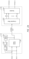
- FIG. 1 is a block diagram of an apparatus 100 according to an embodiment of the present disclosure.
- the apparatus 100 may include a first device 110 that communicates with a second device 120 over an input/output (I/O) bus.
- the first device 110 may include an I/O interface circuit 112 that includes signal driver 114 and receiver and decoder circuit 116 for communication over the I/O bus.
- the second device 120 may include an I/O interface circuit 122 that includes signal driver 124 and receiver and decoder circuit 126 for communication over the I/O bus.
- the I/O bus may support a multilevel communication architecture that includes a plurality of channels. In some embodiments, each channel may be single-ended and may include a single signal line. In other embodiments, each channel may include more than one signal line.
- the first device 110, the second device 120, and the I/O bus may support a channel that includes conversion of M bitstreams to N multilevel signals, where M is greater than N.
- a bitstream includes a plurality of bits provided serially, wherein each bit of the bitstream is provided over a period of time, that may be referred to as a data period. For example, a first bit is provided for a first period, and a second bit is provided for a second period following the first period, and a third bit is provided for a third period following the second period, and so on.
- the successive bits provided in this serial manner represent a stream of bits.
- the corresponding bits of each bitstream for a data period represents data M bits wide.
- the N multilevel signals may be transmitted over the I/O bus.
- Each multilevel signal is provided over a data period having a voltage corresponding to one of multiple voltage levels (e.g., 2 different voltage levels, 4 different voltage levels, 8 different voltage levels, etc.), where each of the multiple voltage levels represents different data.
- 3 bit streams may be converted to 2 tri-level signals.
- pulse-amplitude modulation (PAM) may be used to convert 2, 3, or 4 bitstreams into a single multilevel signal having 4, 8, 16, etc., levels.
- the first device 110 may include a memory controller or processing system and/or the second device 120 may include a memory, including volatile memory and/or non-volatile memory.
- the second device 120 may include a dynamic random access memory (DRAM), such as a double-data-rate (DDR) DRAM or a low power DDR DRAM.
- DRAM dynamic random access memory
- DDR double-data-rate
- a memory is not a necessary component of the disclosure. Rather, the disclosure may be applied to any two or more devices, on or off-chip, that communicate with one another using multilevel signaling.
- the signal driver 114 may include circuitry that applies a bitstream conversion to a set of M bitstreams to generate N multilevel signals and drives the N multilevel signals as channels on the I/O bus.
- the signal driver 124 may include circuitry that applies a bitstream conversion to a set of M bitstreams to generate N multilevel signals and drives the N multilevel signals as channels on the I/O bus.
- the signal driver 114 may include modifications to existing DDR drivers to drive the multilevel signals onto the channels of the I/O bus.
- the receiver and decoder circuit 116 may include decoders configured to recover the set of M bitstreams by decoding the N multilevel signals received via the channels of the I/O bus as provided by the signal driver 124. Further, the receiver and decoder circuit 126 may include decoders configured to recover the set of M bitstreams by decoding the N multilevel signals received via the channels of the I/O bus as provided by the signal driver 114. In some embodiments, the receiver and decoder circuit 116 and the receiver and decoder circuit 126 may include comparators and decoding logic to recover the set of M bitstreams.
- the first device 110 and the second device 120 may communicate over the I/O bus to transfer information, such as data, addresses, commands, etc. While the I/O bus is shown to be bidirectional, the I/O bus may also be a unidirectional bus.
- the I/O interface circuit 112 and I/O interface circuit 122 may implement a multilevel communication architecture. In a multilevel communication architecture, data is sent over a channel during a data period. Data may include a single value on a signal line of a channel, or may be a combination of values provided on a plurality of signal lines of a channel. The data may represent a channel state. A receiver may determine an output signal value based on the value transmitted on the signal line(s) of a channel.
- the signal line value may be compared against one or more reference values to determine the output signal value.
- a receiver has a time period to determine and latch the output signal value from the time the output signal transitions to the current value to the time the output signal transitions to the next value.
- the transition time may be determined based on a clock signal, as well as a setup and hold time based on a transition from one value to another.
- inherent jitter may occur due to differing magnitude shifts (e.g.. from VH to VL vs. from VMID to VH or VL.
- the amount of jitter may be based on the slew rate, the rise/fall times, the multilevel magnitudes values, or combinations thereof.
- the transition times may also be affected by process, voltage, and temperature variations.
- the signal driver 114 may generate data for a channel by converting a bit from each of the M bitstreams during a data period into N multilevel signals.
- the data may be transmitted to the receiver and decoder circuit 126 via N signal lines of the I/O bus.
- the receiver and decoder circuit 126 may detect levels on the N signal lines and decode the levels to retrieve the bit from each of the M streams.
- M is 3 and N is 2, and the signal lines of the I/O bus are capable of being driven to three independent voltage levels. In another example.
- M is 2 and N is 1, and the signal lines of the I/O bus are capable of being driven to four independent voltage levels (e.g., in a PAM implementation).
- Communication protocol between the signal driver 124 and the receiver and decoder circuit 116 may be similar to the communication protocol between the encoder and signal driver 114 and the receiver and decoder circuit 126.
- the signal driver 114 may include a DRAM driver that has been segmented to drive multiple (e.g., more than 2) voltage levels on a signal line.
- FIG 2A is a block diagram of an apparatus for a multilevel communication architecture according to an embodiment of the disclosure.
- the apparatus may include a signal driver 214 coupled to a receiver 226 via an I/O bus.
- the signal driver 214 may be implemented in the signal driver 114 and/or the signal driver 124 of Figure 1 and the receiver 226 may be implemented in the receiver and decoder circuit 116 and/or the receiver and decoder circuit 126 of Figure 1 .
- the signal driver 214 may include a driver circuit 240.
- the driver circuit 240 may receive bitstreams IN ⁇ 1> and IN ⁇ 0> and drive an output signal OUT in response.
- the IN ⁇ 1> and IN ⁇ 0> bitstreams may represent a stream of two-bit data.
- the output signal OUT driven by the driver circuit 240 is based on the IN ⁇ 1> and IN ⁇ 0> bitstreams.
- the signal may be a multilevel signal representing data of the IN ⁇ 0> and IN ⁇ 1> bitstreams.
- the driver circuit 240 may include one or more signal line drivers having a pull-up (e.g., p-type) transistor coupled in series with a pull-down (e.g., n-type) transistor.
- a source of the pull-up transistor is coupled to a high supply voltage and the source of the pull-down transistor is coupled to a low supply voltage.
- the high supply voltage is 1.2 V and the low supply voltage is ground.
- the output signal OUT is provided at a common node to which the pull-up and pull-down transistors are coupled.
- Gates of the pull-up and pull-down transistors of the driver circuit 240 are provided with the IN ⁇ 1> and IN ⁇ 0> bitstreams. In other embodiments of the disclosure, the driver circuit 240 may be implemented using other configurations.
- the signal driver 214 further includes a boost control circuit 244 and a boost circuit 246.
- the boost control circuit 244 provides control signals to control the boost circuit 246 according to the IN ⁇ 0> and IN ⁇ 1> bitstreams.
- the boost circuit 244 may be controlled to provide increased pull-down capability and/or increased pull-down capability for the driver circuit 240 based on current data of the IN ⁇ 0> and IN ⁇ 1> bitstreams.
- the receiver 226 may include comparator block 250 coupled to a decoder 260.
- the comparator 250 may be configured to receive the signal from the I/O bus and provide Z0-Zn signals (n is a whole number) to the decoder 260.
- the comparator block 250 may include circuits (not shown in Figure 2A ) configured to compare the signal from the I/O bus against reference signals to provide the Z0-Zn signals.
- the comparator block 250 may include comparators that compare the OUT signal from the I/O bus against various reference signals to provide the Z0-Zn signals.
- the decoder 260 may include logic to generate the bitstreams RX ⁇ 0> and RX ⁇ 1> based on the Z0-Zn signals from the comparator block 250.
- the RX ⁇ 0> and RX ⁇ 1> bitstreams may be logical equivalents of data transmitted by the IN ⁇ 0> and IN ⁇ 1> bitstreams.
- the RX ⁇ 0> and RX ⁇ 1> bitstreams may represent a stream of two-bit received data.
- the IN ⁇ 0> and IN ⁇ 1> may be bitstreams to be transmitted over the I/O bus.
- the signal driver 214 may provide a signal based on the IN ⁇ 0> and IN ⁇ 1> bitstreams to be transmitted over a signal line using a multilevel signal.
- the signal driver 214 may receive the IN ⁇ 0> and IN ⁇ 1> bitstreams, and during each data period, the driver circuit 240 may drive the signal line of the I/O bus with a voltage that will be used by the receiver 226 to provide the RX ⁇ 0> and RX ⁇ 1> bitstreams.
- the multilevel signal may be used to represent data of the IN ⁇ 0> and IN ⁇ 1> bitstreams using fewer signal lines than one signal line per bitstream.
- data of the IN ⁇ 0> and TN ⁇ 1> bitstreams are provided to the receiver 226 on fewer than two signal lines (e.g., one signal on the I/O bus rather than one signal line for the IN ⁇ 0> bitstream and another signal line for the IN ⁇ 1> bitstream).
- Figure 2A illustrates operation with bitstreams IN ⁇ 0> and IN ⁇ 1> for providing bitstreams RX ⁇ 0> and RX ⁇ 1>, the number of bitstreams may be different in other embodiments of the disclosure.
- a third bitstream IN ⁇ 2> may also be provided to the signal driver 214 in addition to the IN ⁇ 0> and IN ⁇ 1> bitstreams and a multilevel signal may be provided over the I/O bus representing the data from the IN ⁇ 0>, IN ⁇ 1>, and IN ⁇ 2> bitstreams.
- a multilevel signal may be provided over the I/O bus representing the data from the IN ⁇ 0>, IN ⁇ 1>, and IN ⁇ 2> bitstreams.
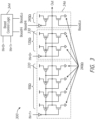
- FIG 3 is a schematic drawing of a signal driver 300 according to an embodiment of the disclosure.
- the signal driver 300 may be used for a multilevel signal architecture implementing pulse-amplitude modulation (PAM).
- PAM pulse-amplitude modulation
- the signal driver 300 may be used as the signal driver 214 in embodiments of the disclosure.
- the signal driver 300 includes a driver circuit including six signal line drivers coupled to a common node that is an output.
- the output may represent an output terminal.
- Each of the signal line drivers are coupled to a high supply voltage (e.g., VDDQ) and to a low supply voltage (e.g., VSSQ).
- the driver circuit may be a driver in a DRAM, such as a double data rate (DDR) DRAM driver.
- DDR double data rate
- each of the signal line drivers has an impedance of 240 ohms.
- the driver circuit may include a first driver section 320 and a second driver section 330 configured to drive an output signal OUT to a common node to which the first and second driver sections 320 and 330 are coupled.
- the first driver section 320 may include four signal line drivers coupled to the common node, each controlled responsive to the IN ⁇ 1> bitstream.
- Each signal line driver may include a pull-up (e.g., p-type) transistor and a pull-down (e.g., n-type) transistor.
- the complement of the IN ⁇ 1> bitstream is provided to the gates of the pull-up and pull-down transistors by an inverter circuit that receives the IN ⁇ 1> bitstream.
- the second driver section 330 may include two signal line drivers coupled to the common node, each controlled responsive to the IN ⁇ 0> bitstream, and each signal line driver may include a pull-up (e.g., p-type) transistor and a pull-down (e.g., n-type) transistor.
- the complement of the IN ⁇ 0> bitstream is provided to the gates of the pull-up and pull-down transistors by an inverter circuit that receives the IN ⁇ 0> bitstream.
- each signal line driver has an impedance of 240 ohms
- the first driver section 320 has an effective impedance of 60 ohms
- the second driver section 330 has an effective impedance of 120 ohms. With each of the signal line drivers having the same impedance, the signal line drivers have the same drive strength.
- the signal driver 300 further includes a boost circuit 346 that receives control signals BoostHi and BoostLo from boost control circuit 344.
- the boost control circuit 344 includes logic circuits and provides control signals BoostHi and BoostLo to the boost circuit 346 based on the IN ⁇ 0> and IN ⁇ 1> bitstreams.
- a BoostHi signal or BoostLo signal having the high logic level is represented by a signal of 1.2 V.
- a BoostHi signal or BoostLo signal having the low logic level is represented by a signal of 0 V.
- other voltage levels may be used to represent the "1" and "0" data in other embodiments of the disclosure.
- the boost circuit 346 is coupled to the common node and includes a pull-up (e.g., p-type) transistor and a pull-down (e.g., n-type) transistor, which are controlled by the BoostHi and BoostLo signals, respectively.
- the boost circuit 346 may also be referred to as another driver section of the driver circuit.
- the complement of the BoostHi signal is provided to the gate of the pull-up transistor by an inverter circuit that receives the BoostHi signal.
- the BoostHi signal provided by the boost control circuit 344 is active when at a high logic level to activate the pull-up transistor and the BoostLo signal is active when at a high logic level to activate the pull-down transistor.
- the pull-up transistor When activated by an active BoostHi signal from the boost control circuit 344, the pull-up transistor provides additional drive to pull up the level of the signal line. Similarly, when activated by an active BoostLo signal from the boost control circuit 344, the pull-down transistor provides additional drive to pull down the level of the signal line.
- the first driver section 320 has an effective impedance of 60 ohms
- the second driver section 330 has an effective impedance of 120 ohms.
- the boost circuit 346 would have an impedance of 240 ohms.
- the first driver section 320, second driver section 330, and boost circuit e.g., third driver section
- the pull-up transistor of the boost circuit 346 may be activated when the IN ⁇ 1> and IN ⁇ 0> bitstreams represent data corresponding to a voltage level of a high supply voltage (e.g., representing data "11"), and the pull-down transistor may be activated when the IN ⁇ 1> and IN ⁇ 0> bitstreams represent data corresponding to a voltage level of a low supply voltage (e.g., representing data "00").
- Figure 3 shows the boost circuit 346 as including one pull-up transistor and one pull-down transistor, in other embodiments of the disclosure, the boost circuit 346 may include a greater number of pull-up and/or pull-down transistors.
- the embodiment of Figure 3 is not intended to limit boost circuits, or more generally, driver circuits, to embodiments having the specific configuration shown in Figure 3 .
- PAM4 is used to convert two bitstreams (e.g., the IN ⁇ 1> and IN ⁇ 0> bitstreams) into an OUT signal having one of four different voltage levels.
- the IN ⁇ 1> bitstream may be provided to the signal line drivers of the first driver section 320 and the IN ⁇ 0> bitstream may be provided to the signal line drivers of the second driver section 330.
- the resulting output signal will have one of four different voltages corresponding to the data of the IN ⁇ 1> and IN ⁇ 0> bitstreams.
- a current data of the IN ⁇ 1> and IN ⁇ 0> bitstreams is a "00"
- the pull-down transistors of both the driver sections 320 and 330 are activated to drive (e.g., pull down) the common node to the low supply voltage to provide an output signal OUT having the voltage of the low supply voltage.
- a current data of "00” also causes the pull-down transistor of the boost circuit 346 to provide additional drive to pull down the common node to the low supply voltage.
- a current data of the IN ⁇ 1> and IN ⁇ 0> bitstream is a "11”
- the pull-up transistors of both the driver sections 320 and 330 are activated to drive (e.g., pull up) the common node to the high supply voltage to provide an output signal OUT having the voltage of the high supply voltage.
- a current data of "11” also causes the pull-up transistor of the boost circuit 346 to provide additional drive to pull up the common node to the high supply voltage.
- the pull-up transistor of the boost circuit 346 is activated to drive the common node to the high supply voltage when the first and second driver sections 320 and 330 drive the common node to the high supply voltage.
- the pull-down transistor of the boost circuit 346 is activated to drive the common node to the low supply voltage when the first and second driver sections 320 and 330 drive the common node to the low supply voltage.
- the pull-down transistors of the driver section 320 are activated and the pull-down transistors of the driver section 330 are activated to provide a voltage to the common node that results in an output signal OUT having an intermediate-low voltage.
- the pull-up transistors of the driver section 320 are activated and the pull-down transistors of the driver section 330 are activated to provide a voltage to the common node that results in an output signal OUT having an intermediate-high voltage.
- neither the pull-up nor pull-down transistors of the boost circuit 346 are activated to provide any additional drive to change the voltage of the common node. With both the pull-up and pull-down transistors of the boost circuit 346 deactivated, the boost circuit 346 is in a high-impedance state.
- first driver section 320, the second driver section 330, and the boost circuit 346 are shown in Figure 3 as including p-type pull-up transistors and n-type pull-down transistors. That is, the pull-up and pull-down transistors have different conductivity types.
- the first driver section 320, the second driver section 330, and the boost circuit 346 may include n-type pull-up transistors, or a combination of p-type and n-type pull-up transistors.
- n-type pull-up transistors which are activated by a high logic level signal (e.g., having the high supply voltage)
- the logic level of the signals provided to gates of the n-type pull-up transistors will have a complementary logic level to signals provided to the gates of p-type pull-up transistors.
- a signal having a complementary logic level may be provided by using an inverter circuit.
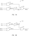
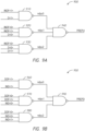
- FIG 4A is a schematic diagram of a boost control circuit 410 according to an embodiment of the disclosure.
- the boost control circuit 410 may be included in the boost control circuit 344 of the signal driver 300 of Figure 3 in some embodiments of the disclosure.
- the boost control circuit 410 may control the boost circuit 346 to provide additional drive capability to the driver sections 320 and 330 drive the common node to provide a voltage level of the high supply voltage (e.g., when the IN ⁇ 1> and IN ⁇ 0> bitstreams represent "11" data).
- the boost control circuit 410 includes an AND logic circuit that receives the IN ⁇ 1> and IN ⁇ 0> bitstreams and provides the BoostHi signal resulting from a logic AND operation of the IN ⁇ 1> and IN ⁇ 0> bitstreams.
- the boost control circuit 410 provides an active BoostHi signal (e.g., active when a high logic level) when the current data represented by the IN ⁇ 1> and IN ⁇ 0> bitstreams is "11", which causes the signal driver 300 to provide the output signal OUT having the voltage of the high supply voltage (e.g., current data of the IN ⁇ 1> and IN ⁇ 0> bitstreams is "11").
- active BoostHi signal e.g., active when a high logic level
- the high logic level of the IN ⁇ 1> bitstream is provided to the line drivers of the first driver section 320 to cause the pull-up transistors to be activated and the high logic level of the IN ⁇ 0> bitstream is provided to the line drivers of the second driver section 330 to cause the pull-up transistors to be activated.
- the common node to which the first and second driver sections 320 and 330 are coupled is pulled up to the voltage of the high supply voltage.
- the high logic levels of the IN ⁇ 1> and IN ⁇ 0> bitstreams are provided to the AND logic circuit of the boost control circuit 410 and a logical AND operation is performed to provide an active (e.g..
- BoostHi BoostHi signal.
- the pull-up transistor of the boost circuit 346 is activated by the active BoostHi signal to provide additional drive to further pull up the common node to the voltage of the high supply voltage.
- the pull-up transistor of the boost circuit 346 is activated to assist in pulling up the common node when the output signal OUT is to be provided having the voltage of the high supply voltage.
- FIG 4B is a schematic diagram of a boost control circuit 420 according to an embodiment of the disclosure.
- the boost control circuit 420 may be included in the boost control circuit 344 of the signal driver 300 of Figure 3 in some embodiments of the disclosure.
- the boost control circuit 420 may control the boost circuit 346 to provide additional drive capability to the driver sections 320 and 330 drive the common node to provide a voltage level of the low supply voltage (e.g., when the IN ⁇ 1> and IN ⁇ 0> bitstreams represent "00" data).
- the boost control circuit 420 includes an exclusive OR (XOR) logic circuit 430 that receives the IN ⁇ 1> and IN ⁇ 0> bitstreams and an inverter circuit 440 that receives the IN ⁇ 0> bitstream.
- XOR exclusive OR
- the signals provided by the XOR logic circuit 430 and the inverter circuit 440 are provided to an AND logic circuit 450 which provides the BoostLo signal resulting from a logic AND operation of the signals provided by the XOR logic circuit 430 and the inverter circuit 440.
- the boost control circuit 420 provides an active BoostLo signal (e.g., active when a high logic level) when the current data represented by the IN ⁇ 1> and IN ⁇ 0> bitstreams is a "00", which causes the signal driver 300 to provide the output signal OUT having the voltage of the low supply voltage (e.g., current data of the IN ⁇ 1> and IN ⁇ 0> bitstreams is "00").
- active BoostLo signal e.g., active when a high logic level
- the low logic level of the IN ⁇ 1> bitstream is provided to the line drivers of the first driver section 320 to cause the pull-down transistors to be activated and the low logic level of the IN ⁇ 0> bitstream is provided to the line drivers of the second driver section 330 to cause the pull-down transistors to be activated.
- the common node to which the first and second driver sections 320 and 330 are coupled is pulled up to the voltage of the low supply voltage.
- the low logic levels of the IN ⁇ 1> and IN ⁇ 0> bitstreams are provided to the XOR logic circuit 430 of the boost control circuit 420 and the IN ⁇ 0> bitstream is provided to the inverter circuit 440.
- the outputs of the XOR logic circuit 430 and the inverter circuit 440 are provided to the AND logic circuit 450, and a logical NAND operation is performed to provide an active (e.g., a high logic level) BoostLo signal.
- the pull-down transistor of the boost circuit 346 is activated by the active BoostLo signal to provide additional drive to further pull down the common node to the voltage of the low supply voltage.
- the pull-down transistor of the boost circuit 346 is activated to assist in pulling down the common node when the output signal OUT is to be provided having the voltage of the low supply voltage.
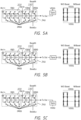
- Figure 5A is a diagram showing operation of the first and second driver sections 320 and 330, and the boost circuit 346, of the signal driver 300 for driving a load that is terminated to a high supply voltage (e.g., VDDQ) according to an embodiment of the disclosure.
- a typical signal driver may not fully drive an output signal OUT to a low supply voltage (e.g., VSSQ, as shown as "w/o Boost").
- the high supply voltage may represent a high logic level (e.g., "11") output signal OUT and the low supply voltage may represent a low logic level (e.g., "00") output signal OUT in some embodiments of the disclosure.
- the inability for the signal driver to fully drive the output signal OUT to the high supply voltage may be due to, for example, variations in circuit performance.
- the variation in circuit performance may be due to variations in the process when fabricating the circuits, variations in the supply voltages powering the circuits, and/or operating temperature of the circuits. As a result, actual circuit performance may deviate from ideal circuit performance. By not fully driving the output signal OUT to the low supply voltage, the voltage margin between the different voltage levels representing the different data is reduced, which may be more susceptible to data errors.
- the boost circuit 346 may be used to assist driving the output signal OUT.
- the pull-down transistor of the boost circuit 346 may be used to provide additional drive to fully drive the output signal OUT to the low supply voltage when the signal driver 300 provides an output signal OUT having a low logic level.
- the pull-down transistor of the boost circuit 346 may be activated by an active BoostLo signal, which may be provided by boost control circuit (e.g., boost control circuit 344).
- the BoostLo signal may be active when the signal driver 300 is driving a low logic level output signal OUT.
- Figure 5B is a diagram showing operation of the first and second driver sections 320 and 330, and the boost circuit 346, of the signal driver 300 for driving a line terminated load according to an embodiment of the disclosure.
- a typical signal driver may not fully drive an output signal OUT to either a high or low supply voltage (e.g., VDDQ or VSSQ, as shown as “w/o Boost").
- the high supply voltage may represent a high logic level (e.g., "11") output signal OUT and the low supply voltage may represent a low logic level (e.g., "00") output signal OUT in some embodiments of the disclosure.
- the inability for the signal driver to fully drive the output signal OUT to the high supply voltage may be due to, for example, variations in circuit performance.
- the variation in circuit performance may be due to variations in the process when fabricating the circuits, variations in the supply voltages powering the circuits, and/or operating temperature of the circuits. As a result, actual circuit performance may deviate from ideal circuit performance.
- by not fully driving the output signal OUT to either of the high or low supply voltages the voltage margin between the different voltage levels representing the different data is reduced, which may be more susceptible to data errors.
- the boost circuit 346 may be used to assist driving the output signal OUT.
- the pull-down transistor of the boost circuit 346 may be used to provide additional drive to fully drive the output signal OUT to the low supply voltage when the signal driver 300 provides an output signal OUT having a low logic level.
- the pull-up transistor of the boost circuit 346 may be used to provide additional drive to fully drive the output signal OUT to the high supply voltage when the signal driver 300 provides an output signal OUT having a high logic level.
- the pull-down transistor of the boost circuit 346 may be activated by an active BoostLo signal and the pull-up transistor of the boost circuit 346 may be activated by an active BoostHi signal.
- the BoostLo and BoostHi signals may be provided by a boost control circuit (e.g., boost control circuit 344).
- the BoostLo signal may be active when the signal driver 300 is driving a low logic level output signal OUT and the BoostHi signal may be active when the signal driver 300 is driving a high logic level output signal OUT.
- Figure 5C is a diagram showing operation of the first and second driver sections 320 and 330, and the boost circuit 346. of the signal driver 300 for driving a load that is terminated to a low supply voltage (e.g., VSSQ) according to an embodiment of the disclosure.
- a typical signal driver may not fully drive an output signal OUT to a high supply voltage (e.g., VDDQ. as shown as "w/o Boost").
- the high supply voltage may represent a high logic level (e.g., "11") output signal OUT and the low supply voltage may represent a low logic level (e.g., "00") output signal OUT in some embodiments of the disclosure.
- the boost circuit 346 may be used to assist driving the output signal OUT.
- the pull-up transistor of the boost circuit 346 may be used to provide additional drive to fully drive the output signal OUT to the high supply voltage when the signal driver 300 provides an output signal OUT having a high logic level.
- the pull-up transistor of the boost circuit 346 may be activated by an active BoostHi signal, which may be provided by boost control circuit (e.g., boost control circuit 344).
- the BoostHi signal may be active when the signal driver 300 is driving a high logic level output signal OUT.
- the boost circuit 346 may provide additional drive for data corresponding to just one of the supply voltages. For example, in some embodiments of the disclosure, data corresponding to the low supply voltage is boosted, but data corresponding to the high supply voltage is not.
- the pull-up transistor of the boost circuit 346 may be disabled, circuits for providing signals to activate a pull-up transistor of the boost circuit 346 may not be included in the boost control circuit, circuits for providing signals to activate a pull-up transistor of the boost circuit 346 may not be enabled, or other approaches may be used to not provide boost for data corresponding to the high supply voltage.
- the pull-down transistor of the boost circuit 346 may be disabled, so that data corresponding to the high supply voltage is boosted, but data corresponding to the low supply voltage is not.
- the pull-down transistor of the boost circuit 346 may be disabled, circuits for providing signals to activate a pull-down transistor of the boost circuit 346 may not be included in the boost control circuit, circuits for providing signals to activate a pull-down transistor of the boost circuit 346 may not be enabled, or other approaches may be used to not provide boost for data corresponding to the low supply voltage.
- the boost circuit 346 is activated to provide additional drive for data corresponding to both the high supply voltage and the low supply voltage. In such embodiments, the boost control circuit 410 and the boost control circuit 420 may be included together.
- Figure 2B is a block diagram of an apparatus for a multilevel communication architecture according to an embodiment of the disclosure.
- the apparatus of Figure 2B is similar to the apparatus of Figure 2A , and consequently, the same reference numbers are used in Figure 2B as in Figure 2A to identify the same components as previously described.
- the apparatus of Figure 2B includes a signal driver 215 coupled to the receiver 226 via an I/O bus.
- the receiver 226 may be as previously described with reference to the apparatus of Figure 2A .
- the signal driver 215 may be implemented in the signal driver 114 and/or the signal driver 124 of Figure 1 and the receiver 226 may be implemented in the receiver and decoder circuit 116 and/or the receiver and decoder circuit 126 of Figure 1 .
- the signal driver 215 may include an input circuit 243 that receives bitstreams IN ⁇ 1> and IN ⁇ 0> and provides output signals to a boost control circuit 245 and a driver circuit 240.
- the driver circuit 240 may be as previously described with reference to the apparatus of Figure 2A .
- the boost control circuit 245 provides control signals to control the boost circuit 247 according to the output signals from the input circuit 243.
- the boost circuit 247 may be controlled to provide increased pull-down capability and/or increased pull-down capability for the driver circuit 240 based on current data of the IN ⁇ 0> and IN ⁇ 1> bitstreams.
- the signal driver 215 may receive the IN ⁇ 0> and IN ⁇ 1> bitstreams, and during each data period, the driver circuit 240 may drive the signal line of the I/O bus with a voltage that will be used by the receiver 226 to provide the RX ⁇ 0> and RX ⁇ 1> bitstreams.
- the multilevel signal may be used to represent data of the IN ⁇ 0> and IN ⁇ 1> bitstreams using fewer signal lines than one signal line per bitstream.
- Figure 2B illustrates operation with bitstreams IN ⁇ 0> and IN ⁇ 1> for providing bitstreams RX ⁇ 0> and RX ⁇ 1>, the number of bitstreams may be different in other embodiments of the disclosure.
- a third bitstream IN ⁇ 2> may also be provided to the signal driver 215 in addition to the IN ⁇ 0> and IN ⁇ 1> bitstreams and a multilevel signal may be provided over the I/O bus representing the data from the IN ⁇ 0>, IN ⁇ 1>, and IN ⁇ 2> bitstreams.
- a multilevel signal may be provided over the I/O bus representing the data from the IN ⁇ 0>, IN ⁇ 1>, and IN ⁇ 2> bitstreams.
- FIG. 6 is a schematic diagram of an input circuit 600 according to an embodiment of the disclosure.
- the input circuit 600 may be included in the input circuit 243 of Figure 2B in some embodiments of the disclosure.
- the input circuit 600 includes D flip-flop circuits 610 and 620, and D flip-flop circuits 640 and 660.
- the D flip-flop circuit 610 receives the IN ⁇ 1> bitstream and the D flip-flop circuit 640 receives the IN ⁇ 0> bitstream.
- the D flip-flop circuit 610 and the D flip-flop circuit 640 are clocked by a clock signal CLK
- the D flip-flop circuit 620 and the D flip-flop circuit 660 are clocked by a clock signal CLKF, which is the complement to the CLK signal.
- the CLK signal may be a system clock signal or a clock signal derived from the system clock signal.
- the system clock signal may be a clock signal provided to different circuits of a larger system in order to synchronize operations, for example, for providing data between the different circuits.
- the D flip-flop circuits 610, 620, 640, and 660 may be reset to provide an output having a known logic level when an active reset signal RST is provided to the D flip-flop circuits.
- the D flip-flop circuits 610, 620, 640, and 660 may be reset, for example, upon reset of the semiconductor device, as part of a power up sequence, etc.
- the D flip-flop circuit 610 latches a current logic level of the IN ⁇ 1> bitstream responsive to a rising edge of the CLK signal and provides an output signal D ⁇ 1> having the same logic level as the latched logic level.
- the D flip-flop circuit 620 latches the logic level of the D ⁇ 1> signal responsive to a rising edge of the CLKF signal and provides an output signal IND ⁇ 1> having the same logic level as the latched logic level.
- the D flip-flop circuit 640 latches a current logic level of the IN ⁇ 0> bitstream responsive to a rising edge of the CLK signal and provides an output signal D ⁇ 0> having the same logic level as the latched logic level.
- the D flip-flop circuit 660 latches the logic level of the D ⁇ 0> signal responsive to a rising edge of the CLKF signal and provides an output signal IND ⁇ 0> having the same logic level as the latched logic level.
- the IN ⁇ 1> and IN ⁇ 0> bitstreams are latched and the D ⁇ 1> and D ⁇ 0> signals provided responsive to a rising edge of the CLK signal
- the D ⁇ 1> and D ⁇ 0> signals are latched and the IND ⁇ 1> and IND ⁇ 0> signals are provided responsive to a falling edge of the CLK signal (i.e., the rising edge of the CLKF signal).
- the IND ⁇ 1> and IND ⁇ 0> signals have the logic levels of the D ⁇ 1> and D ⁇ 0> signals delayed by one-half a clock period of the CLK signal.
- Figure 7A is a schematic diagram of a pull-up logic circuit 700 according to an embodiment of the disclosure.
- the pull-up logic circuit 700 may be included in the boost control circuit 245 of Figure 2B in some embodiments of the disclosure.
- the pull-up logic circuit 700 includes a NAND logic circuit 710 that receives the D ⁇ 1> and D ⁇ 0> signals, for example, from the input circuit 600, and provides an output signal IN_11F that results from a NAND logic operation of the D ⁇ 1> and D ⁇ 0> signals.
- the pull-up logic circuit 700 further includes a NAND logic circuit 720 that receives the IND ⁇ 1> and IND ⁇ 0> signals, for example from the input circuit 600.
- the NAND logic circuit 720 provides an output signal IND_11F resulting from a NAND logic operation on the IND ⁇ 1> and IND ⁇ 0> signals to an inverter circuit 730.
- the inverter circuit 730 provides an output signal IND_11 that is the complement of the IND_11F signal.
- a NOR logic circuit receives the IN_11F signal from the NAND logic circuit 710 and the IND_11 signal from the inverter circuit 730 and provides an output signal PREPU that resulting from a NOR logic operation.
- the logic circuit 700 provides an active PREPU signal (e.g., active high logic level) when the data of the IN ⁇ 1> and IN ⁇ 0> bitstreams changes from a previous value to a current data of "11". That is, where the previous data represented by the IN ⁇ 1> and IN ⁇ 0> bitstreams is "00", “01”, or "10", and the data changes to a current data of "11", the logic circuit 700 provides an active PREPU signal.
- the logic circuit 700 provides and inactive PREPU signal for other changes from a previous data to a current data represented by the IN ⁇ 1> and IN ⁇ 0> bitstreams.
- the logic circuit 700 provides an inactive PREPU signal for the IN ⁇ 1> and IN ⁇ 0> bitstreams changing from a previous data to current data of "00", "01", or "10".
- the active PREPU signal provided by the logic circuit 700 may be used to activate a boost circuit, for example, the boost circuit 346 of the signal driver 300, to provide additional drive to assist driving the common node to the high supply voltage to provide an OUT signal having a voltage of the high supply voltage.
- the PREPU signal is active for a portion of the data period of the OUT signal.
- the PREPU signal is limited to being active to assist the driving of the common node to the high supply voltage.
- the NAND logic circuit 710 provides a low logic level IN_11F signal when D ⁇ 1> and D ⁇ 0> are both a high logic level (i.e., resulting from the IN ⁇ 1> and IN ⁇ 0> bitstreams representing a current data of "11").
- the inverter circuit 730 coupled to the NAND logic circuit 720 to receive the IND_11F signal provides a low logic level IND_11 when IND ⁇ 1> and IND ⁇ 0> are both a high logic level (i.e., resulting from D ⁇ 1> and D ⁇ 0> both a high logic level). Recall that the IND ⁇ 1> and IND ⁇ 0> are delayed relative to D ⁇ 1> and D ⁇ 0>, for example, by one-half a clock period of the CLK signal.
- the NOR logic gate provides an active PREPU signal (e.g. active high logic level) when the IN_11F and IND_11 signals have low logic levels.
- the PREPU signal is active when D ⁇ 1> and D ⁇ 0> are both at a high logic level, and for one-half a clock cycle of the CLK signal following a rising edge of the CLK signal.
- the PREPU signal is active for one-half a clock cycle of the CLK signal because the one-half clock cycle delay of the IND ⁇ 1> and IND ⁇ 0> relative to D ⁇ 1> and D ⁇ 0> will result in the IND_11 signal being at a low logic level while the IN_11F signal is at a low logic level (from D ⁇ 1> and D ⁇ 0> both being a high logic level), but for one-half a clock cycle of the CLK signal before both IND ⁇ 1> and IND ⁇ 0> also become a high logic level (resulting from the D ⁇ 1> and D ⁇ 0> both being at the high logic level).
- the PREPU signal is active for one-half a clock cycle of the CLK signal.
- Figure 7B is a schematic diagram of a pull-down logic circuit 750 according to an embodiment of the disclosure.
- the pull-down logic circuit 750 may be included in the boost control circuit 245 of Figure 2B in some embodiments of the disclosure.
- the pull-down logic circuit 750 includes a NOR logic circuit 760 that receives the D ⁇ 1> and D ⁇ 0> signals, for example, from the input circuit 600, and provides an output signal IN_00 that results from a NOR logic operation of the D ⁇ 1> and D ⁇ 0> signals.
- the IN_00 signal is provided to an inverter circuit 780.
- the inverter circuit 780 provides an output signal IN_00F that is the complement of the IN_00 signal.
- the pull-down logic circuit 750 further includes a NOR logic circuit 770 that receives the IND ⁇ 1> and IND ⁇ 0> signals, for example from the input circuit 600, and provides an output signal IND_00 resulting from a NOR logic operation on the IND ⁇ 1> and IND ⁇ 0> signals.
- a NOR logic circuit receives the IN_00F signal from the inverter circuit 780 and the IND_00 signal from the NOR logic circuit 770 and provides an output signal PREPD that resulting from a NOR logic operation.
- the logic circuit 750 provides an active PREPD signal (e.g., active high logic level) when the data of the IN ⁇ 1> and IN ⁇ 0> bitstreams changes from a previous value to a current data of "00". That is, where the previous data represented by the IN ⁇ 1> and IN ⁇ 0> bitstreams is "01", “10", or "11", and the data changes to a current data of "00", the logic circuit 750 provides an active PREPD signal.
- the logic circuit 750 provides and inactive PREPD signal for other changes from a previous data to a current data represented by the IN ⁇ 1> and IN ⁇ 0> bitstreams.
- the logic circuit 750 provides an inactive PREPD signal for the IN ⁇ 1> and IN ⁇ 0> bitstreams changing from a previous data to current data of "01", "10", or "11".
- the active PREPD signal provided by the logic circuit 750 may be used to activate a boost circuit, for example, the boost circuit 346 of the signal driver 300. to provide additional drive to assist driving the common node to the low supply voltage to provide an OUT signal having a voltage of the low supply voltage.
- the PREPD signal is active for a portion of the data period of the OUT signal.
- the PREPD signal is limited to being active to assist the driving of the common node to the low supply voltage.
- the inverter circuit 780 coupled to the NOR logic circuit 760 provides a low logic level IN_00F signal when D ⁇ 1> and D ⁇ 0> are both a low logic level. (i.e., resulting from the IN ⁇ 1> and IN ⁇ 0> bitstreams representing a current data of "00").
- the NOR logic circuit 770 provides a high logic level IND_00 signal when IND ⁇ 1> and IND ⁇ 0> are both a low logic level (i.e., resulting from D ⁇ 1> and D ⁇ 0> both a low logic level). Recall that the IND ⁇ 1> and IND ⁇ 0> are delayed relative to D ⁇ 1> and D ⁇ 0>, for example, by one-half a clock period of the CLK signal.
- the NOR logic gate 790 provides an active PREPD signal (e.g. active high logic level) when the IN_00F and IND_00 signals have low logic levels.
- the PREPD signal is active when D ⁇ 1> and D ⁇ 0> are both at a low logic level, and for one-half a clock cycle of the CLK signal following a rising edge of the CLK signal.
- the PREPD signal is active for one-half a clock cycle of the CLK signal because the one-half clock cycle delay of the IND ⁇ 1> and IND ⁇ 0> relative to D ⁇ 1> and D ⁇ 0> will result in the IND_00 signal being at a low logic level while the IN_00F signal is at a low logic level (from D ⁇ 1> and D ⁇ 0> both being a low logic level), but for one-half a clock cycle of the CLK signal before both IND ⁇ 1> and IND ⁇ 0> also become a low logic level (resulting from the D ⁇ 1> and D ⁇ 0> both being at the low logic level) and the NOR logic circuit 770 provides a high logic level IND_00.
- the PREPD signal is active for one-half a clock cycle of the CLK signal.
- the boost circuit 346 of the signal driver 300 is activated to provide additional drive for data corresponding to both the high supply voltage and the low supply voltage.
- the boost control circuit 700 and 750 may be used together to control the boost circuit 346.
- Figure 8 is a timing diagram showing various signals during operation of signal driver 300 with the input circuit 600 and pull-up and pull-down logic circuits 700 and 750 according to an embodiment of the disclosure.
- the IND ⁇ 1> signal is provided to the first driver section 320 instead of the IN ⁇ 1> bitstream and the IND ⁇ 0> signal is provided to the second driver section 330 instead of the IN ⁇ 0> bitstream.
- the PREPU and PREPD signals are provided to the boost circuit 346 instead of the BoostHi and BoostLo signals.
- the D flip-flops 610 and 640 of the input circuit 600 are clocked by a rising edge of the CLK signal (shown in Figure 8 as corresponding to a falling edge of the CLKF signal) and the data of the IN ⁇ 1> and IN ⁇ 0> bitstreams is latched to provide the D ⁇ 1> and D ⁇ 0> signals.
- the data at time T0 is "10".
- the D flip-flop 610 provides a high logic level D ⁇ 1> signal and the D flip-flop 640 provides a low logic level D ⁇ 0> signal (not shown in Figure 8 ) shortly after time T0,
- the D flip-flops 620 and 660 of the input circuit 600 are clocked by a rising edge of the CLKF signal (corresponding to a falling edge of the CLK signal).
- the high logic level of the D ⁇ 1> signal is latched by the D flip-flop 620 to provide a high logic level IND ⁇ 1> signal and the low logic level of the D ⁇ 0> signal is latched by the D flip-flop 660 to provide a low logic level IND ⁇ 0> signal (not shown in Figure 8 ) shortly after time T1.
- the IND ⁇ 1> and IND ⁇ 0> signals are provided to the driver circuit 300 to cause the pull-up transistors of the first driver section 320 to be activated and to cause the pull-down transistors of the second driver section 330 to be activated, resulting in providing an OUT signal having an intermediate-high voltage (corresponding to output data of "10") at time TA. Neither the pull-up nor pull-down transistors of the boost circuit 346 are activated by the current data of "10".
- the D flip-flops 610 and 640 of the input circuit 600 are clocked by a rising edge of the CLK signal and the data of the IN ⁇ 1> and IN ⁇ 0> bitstreams is latched to provide the D ⁇ 1> and D ⁇ 0> signals.
- the data at time T2 is "11".
- the D flip-flop 610 maintains a high logic level D ⁇ 1> signal and the D flip-flop 640 provides a high logic level D ⁇ 0> signal (not shown in Figure 8 ) shortly after time T2.
- the NAND logic circuit 710 of the pull-up logic circuit 700 provides a low logic level IN_11F signal due to the high logic levels of the D ⁇ 1> and D ⁇ 0> signals.
- the XOR logic circuit 740 provides an active PREPU signal at time TB.
- the active PREPU signal activates the pull-up transistor of the boost circuit 346 to provide additional drive to pull up the common node in providing the OUT signal.
- the D flip-flops 620 and 660 of the input circuit 600 are clocked by a rising edge of the CLKF signal.
- the high logic level of the D ⁇ 1> signal is latched by the D flip-flop 620 to maintain a high logic level IND ⁇ 1> signal and the high logic level of the D ⁇ 0> signal is latched by the D flip-flop 660 to provide a high logic level IND ⁇ 0> signal (not shown in Figure 8 ) shortly after time T3.
- the IND ⁇ 1> and IND ⁇ 0> signals are provided to the signal driver 300 to cause the pull-up transistors of the first driver section 320 to be activated and to cause the pull-up transistors of the second driver section 330 to be activated, along with the activated pull-up transistor of the boost circuit 346 that provides additional drive to the common node.
- an OUT signal is provided having a voltage of the high supply voltage (corresponding to output data of "11") at time TC.
- the IND_11 signal switches to a high logic level, which causes the XOR logic circuit 740 to provide an inactive PREPU signal.
- the change of the PREPU signal to inactive deactivates the pull-up transistor of the boost circuit 346.
- the boost circuit 346 provides additional drive to pull up the common node to the high supply voltage for a portion of the data period of the OUT signal, for example, during the transition of the OUT signal to the high supply voltage.
- the voltage of the OUT signal changes during the transition from one voltage level to another.
- the D flip-flops 610 and 640 of the input circuit 600 are clocked by a rising edge of the CLK signal and the data of the IN ⁇ 1> and IN ⁇ 0> bitstreams is latched to provide the D ⁇ 1> and D ⁇ 0> signals.
- the data at time T4 is "00".
- the D flip-flop 610 provides a low logic level D ⁇ 1> signal and the D flip-flop 640 provides a low logic level D ⁇ 0> signal (not shown in Figure 8 ) shortly after time T4.
- the inverter circuit 780 of the pull-down logic circuit 750 provides a low logic level IN_00F signal when the NOR logic circuit 760 receives low logic level D ⁇ 1> and D ⁇ 0> signals.
- the IND_00 signal provided by the NAND logic circuit 770 is still at a low logic level from the previous data of "11", which results in the NOR logic circuit 790 providing an active PREPD signal at time TD.
- the active PREPD signal activates the pull-down transistor of the boost circuit 346 to provide additional drive to pull down the common node in providing the OUT signal.
- the D flip-flops 620 and 660 of the input circuit 600 are clocked by a rising edge of the CLKF signal.
- the low logic level of the D ⁇ 1> signal is latched by the D flip-flop 620 to provide a low logic level IND ⁇ 1> signal and the low logic level of the D ⁇ 0> signal is latched by the D flip-flop 660 to provide a low logic level IND ⁇ 0> signal (not shown in Figure 8 ) shortly after time T5.
- the IND ⁇ 1> and IND ⁇ 0> signals are provided to the signal driver 300 to cause the pull-down transistors of the first driver section 320 to be activated and to cause the pull-down transistors of the second driver section 330 to be activated, along with the activated pull-down transistor of the boost circuit 346 that provides additional drive to the common node.
- an OUT signal is provided having a voltage of the low supply voltage (corresponding to output data of "00") at time TE.
- the boost circuit 346 provides additional drive to pull down the common node to the low supply voltage for a portion of the data period of the OUT signal, for example, during the transition of the OUT signal to the low supply voltage. As previously described, the voltage of the OUT signal changes during the transition from one voltage level to another.
- the D flip-flops 610 and 640 of the input circuit 600 are clocked by a rising edge of the CLK signal and the data of the IN ⁇ 1> and IN ⁇ 0> bitstreams is latched to provide the D ⁇ 1> and D ⁇ 0> signals.
- the data at time T6 is "11".
- the D flip-flop 610 provides a high logic level D ⁇ 1> signal and the D flip-flop 640 provides a high logic level D ⁇ 0> signal (not shown in Figure 8 ) shortly after time T6.
- the pull-up logic circuit 700 responds by providing an active PREPU signal at time TF to activate the pull-up transistor of the boost circuit 346 to provide additional drive to pull up the common node in providing the OUT signal.
- the D flip-flops 620 and 660 of the input circuit 600 are clocked by a rising edge of the CLKF signal.
- the high logic level of the D ⁇ 1> signal is latched by the D flip-flop 620 to provide a high logic level IND ⁇ 1> signal and the high logic level of the D ⁇ 0> signal is latched by the D flip-flop 660 to provide a high logic level IND ⁇ 0> signal (not shown in Figure 8 ) shortly after time T7.
- the pull-up transistors of the first and second driver sections 320 and 330 of the signal driver circuit 300 are activated, along with the activated pull-up transistor of the boost circuit 346 to drive the common node to the voltage of the high supply voltage and provide an OUT signal having a voltage of the high supply voltage (corresponding to output data of "11") at time TG.
- the IND ⁇ 1> and IND ⁇ 0> signals propagate through the NAND logic circuit 720 and the inverter circuit 730 of the pull-up logic circuit 700, the IND_11 signal switches to a high logic level and the XOR logic circuit 740 provides an inactive PREPU signal.
- the inactive PREPU signal deactivates the pull-up transistor of the boost circuit 346.
- the D flip-flops 610 and 640 of the input circuit 600 are clocked by a rising edge of the CLK signal and the data of the IN ⁇ 1> and IN ⁇ 0> bitstreams is latched to provide the D ⁇ 1> and D ⁇ 0> signals.
- the data at time T0 is "01".
- the D flip-flop 610 provides a low logic level D ⁇ 1> signal and the D flip-flop 640 provides a high logic level D ⁇ 0> signal (not shown in Figure 8 ) shortly after time T8.
- the D flip-flops 620 and 660 of the input circuit 600 are clocked by a rising edge of the CLKF signal.
- the low logic level of the D ⁇ 1> signal is latched by the D flip-flop 620 to provide a low logic level IND ⁇ 1> signal and the high logic level of the D ⁇ 0> signal is latched by the D flip-flop 660 to provide a high logic level IND ⁇ 0> signal (not shown in Figure 8 ) shortly after time T9.
- the IND ⁇ 1> and IND ⁇ 0> signals are provided to the signal driver 300 to cause the pull-down transistors of the first driver section 320 to be activated and to cause the pull-up transistors of the second driver section 330 to be activated, resulting in providing an OUT signal having an intermediate-low voltage (corresponding to output data of "01") at time TH. Neither the pull-up nor pull-down transistors of the boost circuit 346 are activated by the current data of "01".
- Figure 9A is a schematic diagram of a pull-up logic circuit 900 according to an embodiment of the disclosure.
- the pull-up logic circuit 900 may be included in the boost control circuit 245 of Figure 2B in some embodiments of the disclosure.
- the pull-up logic circuit 900 includes a NAND logic circuit 910 that receives the D ⁇ 1> and INDF ⁇ 1> signals.
- the input circuit 600 may provide the D ⁇ 1> signal, and the input circuit 600 may further provide an IND ⁇ 1> signal.
- the INDF ⁇ 1> signal is the complement of the IND ⁇ 1> signal, and may be provided by an inverter circuit (not shown) that receives the IND ⁇ 1> signal from the input circuit 600 and provides the INDF ⁇ 1> signal.
- the NAND logic circuit 920 provides an output signal ndpu1 that results from a NAND logic operation of the D ⁇ 0>, INDF ⁇ 1>, and INDF ⁇ 0> signals.
- the NAND logic circuit 930 receives the D ⁇ 1>, D ⁇ 0>, and INDF ⁇ 0> signals.
- the NAND logic circuit 930 provides an output signal ndpu2 that results from a NAND logic operation of the D ⁇ 1>, D ⁇ 0>, and INDF ⁇ 0> signals.
- a NAND logic circuit 940 receives the ndpu0, ndpul, and ndpu2 signals from the NAND logic circuits 910. 920, and 930 and provides an output signal PREPU that results from a NAND logic operation.
- the PREPU signal may be used to control the pull-up transistor of the boost circuit 346.
- the pull-up logic circuit 900 provides an active PREPU signal (e.g., active high logic level) when the data of the IN ⁇ 1> and IN ⁇ 0> bitstreams changes from a previous data to a current data that is represented by a higher voltage than the previous data.
- an active PREPU signal e.g., active high logic level
- the pull-up logic circuit 900 provides an active PREPU signal for a current data of "01”, “10”, and “11”, where the previous data represented by the IN ⁇ 1> and IN ⁇ 0> bitstreams is "01”, the pull-up logic circuit 900 provides an active PREPU signal for a current data of "10” and “11”: and where the previous data represented by the IN ⁇ 1> and IN ⁇ 0> bitstreams is "10”, the pull-up logic circuit 900 provides an active PREPU signal for a current data of "11".
- the active PREPU signal provided by the logic circuit 900 may be used to activate a boost circuit, for example, the boost circuit 346 of the signal driver 300.
- the PREPU signal is active for a portion of the data period of the OUT signal.
- the PREPU signal is limited to being active to assist the driving of the common node during a transition to a higher voltage when changing to current data that is represented by a higher voltage than the previous data. That is, the voltage of the OUT signal changes during the transition from one voltage level to another.
- Figure 9B is a schematic diagram of a pull-down logic circuit 950 according to an embodiment of the disclosure.
- the pull-down logic circuit 950 may be included in the boost control circuit 245 of Figure 2B in some embodiments of the disclosure.
- the pull-down logic circuit 950 includes a NAND logic circuit 960 that receives the IND ⁇ 1> and DDF ⁇ 1> signals.
- the input circuit 600 may provide the IND ⁇ 1> signal, and the input circuit 600 may further provide a D ⁇ 1> signal.
- the DDF ⁇ 1> signal is the complement of the D ⁇ 1> signal, and may be provided by an inverter circuit (not shown) that receives the D ⁇ 1> signal from the input circuit 600 and provides the DDF ⁇ 1> signal.
- the NAND logic circuit 960 provides an output signal ndpd0 that results from a NAND logic operation of the DDF ⁇ 1> and IND ⁇ 1> signals.
- the pull-down logic circuit 950 further includes NAND logic circuits 970 and 980.
- the NAND logic circuit 970 receives the IND ⁇ 0>, DDF ⁇ 1>, DDF ⁇ 0> signals.
- the input circuit 600 may provide the IND ⁇ 0> signal, and the input circuit 600 may further provide a D ⁇ 0> signal.
- the DDF ⁇ 0> signal is the complement of the D ⁇ 0> signal, and may be provided by an inverter circuit (not shown) that receives the D ⁇ 0> signal from the input circuit 600 and provides the DDF ⁇ 0> signal.
- the NAND logic circuit 970 provides an output signal ndpd1 that results from a NAND logic operation of the IND ⁇ 0>, DDF ⁇ 1>, and DDF ⁇ 0> signals.
- the NAND logic circuit 980 receives the IND ⁇ 1>, IND ⁇ 0>, and DDF ⁇ 0> signals.
- the NAND logic circuit 980 provides an output signal ndpd2 that results from a NAND logic operation of the IND ⁇ 1>, IND ⁇ 0>, and DDF ⁇ 0> signals.
- a NAND logic circuit 990 receives the ndpd0. ndpd1. and ndpd2 signals from the NAND logic circuits 960, 970, and 980 and provides an output signal PREPD that results from a NAND logic operation.
- the PREPD signal may be used to control the pull-down transistor of the boost circuit 346.
- the pull-down logic circuit 950 provides an active PREPD signal (e.g., active high logic level) when the data of the IN ⁇ 1> and IN ⁇ 0> bitstreams changes from a previous data to a current data that is represented by a lower voltage than the previous data.
- an active PREPD signal e.g., active high logic level
- the pull-down logic circuit 950 provides an active PREPD signal for a current data of "00", “01”, and “10”; where the previous data represented by the IN ⁇ 1> and IN ⁇ 0> bitstreams is “10”, the pull-down logic circuit 950 provides an active PREPD signal for a current data of "01” and "00”: and where the previous data represented by the IN ⁇ 1> and IN ⁇ 0> bitstreams is "01”, the pull-up logic circuit 950 provides an active PREPD signal for a current data of "00".
- the active PREPD signal provided by the logic circuit 950 may be used to activate a boost circuit, for example, the boost circuit 346 of the signal driver 300, to provide additional drive to assist driving the common node to a lower voltage to provide an OUT signal.
- the PREPD signal is active for a portion of the data period of the OUT signal.
- the PREPD signal is limited to being active to assist the driving of the common node during a transition to a lower voltage when changing to current data that is represented by a lower voltage than the previous data. That is, the voltage of the OUT signal changes during the transition from one voltage level to another.
- Figure 10 is a timing diagram showing various signals during operation of signal driver 300 with the input circuit 600 and pull-up and pull-down logic circuits 900 and 950 according to an embodiment of the disclosure.
- the IND ⁇ 1> signal is provided to the first driver section 320 instead of the IN ⁇ 1> bitstream and the IND ⁇ 0> signal is provided to the second driver section 330 instead of the IN ⁇ 0> bitstream.
- the PREPU and PREPD signals are provided to the boost circuit 346 instead of the BoostHi and BoostLo signals.
- the output is terminated to a high supply voltage, resulting in "11" data represented by 1.2 V, "10” data represented by 1.0 V, "01” data represented by 0.8 V, and "00" data represented by 0.6 V.
- Other embodiments of the disclosure may use other voltage levels to represent the data values.
- the D flip-flops 610 and 640 of the input circuit 600 are clocked by a rising edge of the CLK signal (shown in Figure 10 as corresponding to a falling edge of the CLKF signal) and the data of the IN ⁇ 1> and IN ⁇ 0> bitstreams is latched to provide the D ⁇ 1> and D ⁇ 0> signals.
- the previous data prior to time T0 is "01" and the current data at time T0 is "10".
- Latching of the current data "10" results in the D flip-flop 610 providing a high logic level D ⁇ 1> signal and the D flip-flop 640 providing a low logic level D ⁇ 0> signal (not shown in Figure 10 ) shortly after time T0.
- the INDF ⁇ 1> is at a high logic level and the INDF ⁇ 0> signal is at a low logic level based on the previous data due to the D flip-flops 620 and 660 of the input circuit not yet clocked by a rising edge of the CLKF signal.
- the NAND logic circuit 940 provides an active PREPU signal at time TA.
- the active PREPU signal activates the pull-up transistor of the boost circuit 346 to provide additional drive to pull up the common node in providing the OUT signal.
- the boost circuit 346 is activated to assist with driving the common node to a higher voltage when the data of the IN ⁇ 1> and IN ⁇ 0> bitstreams changes from a previous data to a current data that is represented by a higher voltage than the previous data, such as in the present example where the previous data was "01" and the current data is "10".
- the D flip-flops 620 and 660 of the input circuit 600 are clocked by a rising edge of the CLKF signal (corresponding to a falling edge of the CLK signal).
- the high logic level of the D ⁇ 1> signal is latched by the D flip-flop 620 to provide a high logic level IND ⁇ 1> signal (also resulting in a low logic level INDF ⁇ 1> signal) and the low logic level of the D ⁇ 0> signal is latched by the D flip-flop 660 to provide a low logic level IND ⁇ 0> signal (not shown in Figure 10 , also resulting in a high logic level INDF ⁇ 0> signal) shortly after time T1.
- the IND ⁇ 1> and IND ⁇ 0> signals are provided to the signal driver 300 to cause the pull-up transistors of the first driver section 320 to be activated and to cause the pull-down transistors of the second driver section 330 to be activated, along with the activated pull-up transistor of the boost circuit 346 that provides additional drive to the common node.
- an OUT signal is provided having an intermediate-high voltage (corresponding to output data of "10") at time TB.
- the change of the PREPU signal to inactive deactivates the pull-up transistor of the boost circuit 346.
- the boost circuit 346 provides additional drive to pull up the common node for a portion of the data period of the OUT signal, for example, during the transition of the OUT signal to a higher voltage.
- the voltage of the OUT signal changes during the transition from one voltage level to another.
- the D flip-flops 610 and 640 of the input circuit 600 are clocked by a rising edge of the CLK signal and the data of the IN ⁇ 1> and IN ⁇ 0> bitstreams is latched to provide the D ⁇ 1> and D ⁇ 0> signals.
- the previous data prior to time T2 is "10" and the current data at time T2 is "11". Latching of the current data "11" results in the D flip-flop 610 providing a high logic level D ⁇ 1> signal and the D flip-flop 640 providing a high logic level D ⁇ 0> signal (not shown in Figure 10 ) shortly after time T2.
- the INDF ⁇ 1> is at a low logic level and the INDF ⁇ 0> signal is at a high logic level based on the previous data due to the D flip-flops 620 and 660 of the input circuit not yet clocked by a rising edge of the CLKF signal.
- the NAND logic circuit 940 provides an active PREPU signal at time TC to activate the pull-up transistor of the boost circuit 346 and provide additional drive to pull up the common node in providing the OUT signal.
- the activated boost circuit 346 assists with driving the common node to a higher voltage of the current data "11" from the voltage of the previous data "10".
- the D flip-flops 620 and 660 of the input circuit 600 are clocked by a rising edge of the CLKF signal.
- the high logic level of the D ⁇ 1> signal is latched by the D flip-flop 620 to provide a high logic level IND ⁇ 1> signal (also resulting in a low logic level INDF ⁇ 1> signal) and the high logic level of the D ⁇ 0> signal is latched by the D flip-flop 660 to provide a high logic level IND ⁇ 0> signal (not shown in Figure 10 , also resulting in a low logic level INDF ⁇ 0> signal) shortly after time T3.
- the IND ⁇ 1> and IND ⁇ 0> signals are provided to the signal driver 300 to cause the pull-up transistors of the first and second driver sections 320 and 330 to be activated, along with the activated pull-up transistor of the boost circuit 346 that provides additional drive to the common node.
- an OUT signal is provided having the high supply voltage (corresponding to output data of "11") at time TD.
- the PREPU signal changes to inactive to deactivate the pull-up transistor of the boost circuit 346 after providing additional drive to pull up the common node during the transition of the OUT signal to a higher voltage.
- the voltage of the OUT signal changes during the transition from one voltage level to another.
- the D flip-flops 610 and 640 of the input circuit 600 are clocked by a rising edge of the CLK signal and the data of the IN ⁇ 1> and IN ⁇ 0> bitstreams is latched to provide the D ⁇ 1> and D ⁇ 0> signals.
- the previous data prior to time T4 is "11" and the current data at time T4 is "00".
- Latching of the current data "00" results in the D flip-flop 610 providing a low logic level D ⁇ 1> signal and the D flip-flop 640 providing a low logic level D ⁇ 0> signal (not shown in Figure 10 ) shortly after time T4.
- the DDF ⁇ 1> signal is a high logic level and the DDF ⁇ 0> signal is a high logic level.
- the IND ⁇ 1> is at a high logic level and the IND ⁇ 0> signal is at a high logic level based on the previous data due to the D flip-flops 620 and 660 of the input circuit not yet clocked by a rising edge of the CLKF signal.
- the NAND logic circuit 990 provides an active PREPD signal at time TE to activate the pull-down transistor of the boost circuit 346 and provide additional drive to pull down the common node in providing the OUT signal.
- the activated boost circuit 346 assists with driving the common node to a lower voltage of the current data "00" from the voltage of the previous data "11".
- the D flip-flops 620 and 660 of the input circuit 600 are clocked by a rising edge of the CLKF signal.
- the low logic level of the D ⁇ 1> signal is latched by the D flip-flop 620 to provide a low logic level IND ⁇ 1> signal and the low logic level of the D ⁇ 0> signal is latched by the D flip-flop 660 to provide a low logic level IND ⁇ 0> signal (not shown in Figure 10 ) shortly after time T5.
- the IND ⁇ 1> and IND ⁇ 0> signals are provided to the signal driver 300 to cause the pull-down transistors of the first and second driver sections 320 and 330 to be activated, along with the activated pull-down transistor of the boost circuit 346 that provides additional drive to the common node.
- an OUT signal is provided having a voltage of the low supply voltage (corresponding to output data of "00") at time TF.
- the PREPD signal changes to inactive.
- the change of the PREPD signal to inactive deactivates the pull-down transistor of the boost circuit 346.
- the boost circuit 346 provides additional drive to pull down the common node for a portion of the data period of the OUT signal, for example, during the transition of the OUT signal to a lower voltage.
- the voltage of the OUT signal changes during the transition from one voltage level to another.
- the D flip-flops 610 and 640 of the input circuit 600 are clocked by a rising edge of the CLK signal and the data of the IN ⁇ 1> and IN ⁇ 0> bitstreams is latched to provide the D ⁇ 1> and D ⁇ 0> signals.
- the previous data prior to time T6 is "11" and the current data at time T6 is "10".
- Latching of the current data "10” results in the D flip-flop 610 providing a high logic level D ⁇ 1> signal and the D flip-flop 640 providing a low logic level D ⁇ 0> signal (not shown in Figure 10 ) shortly after time T6.
- the DDF ⁇ 1> signal is a low logic level and the DDF ⁇ 0> signal is a high logic level.
- the IND ⁇ 1> is at a high logic level and the IND ⁇ 0> signal is at a high logic level based on the previous data due to the D flip-flops 620 and 660 of the input circuit not yet clocked by a rising edge of the CLKF signal.
- the NAND logic circuit 990 provides an active PREPD signal at time TG to activate the pull-down transistor of the boost circuit 346 and provide additional drive to pull down the common node in providing the OUT signal.
- the activated boost circuit 346 assists with driving the common node to a lower voltage of the current data "10" from the voltage of the previous data "11".
- the D flip-flops 620 and 660 of the input circuit 600 are clocked by a rising edge of the CLKF signal.
- the high logic level of the D ⁇ 1> signal is latched by the D flip-flop 620 to provide a high logic level IND ⁇ 1> signal and the low logic level of the D ⁇ 0> signal is latched by the D flip-flop 660 to provide a low logic level IND ⁇ 0> signal (not shown in Figure 10 ) shortly after time T7.
- the IND ⁇ 1> and IND ⁇ 0> signals are provided to the signal driver 300 to cause the pull-up transistors of the first driver section 320 to be activated and the pull-down transistors of the second driver section 330 to be activated, along with the activated pull-down transistor of the boost circuit 346 that provides additional drive to the common node.
- an OUT signal is provided having an intermediate-high voltage (corresponding to output data of "10") at time TH.
- the change of the PREPD signal to inactive deactivates the pull-down transistor of the boost circuit 346.
- the boost circuit 346 provides additional drive to pull down the common node for a portion of the data period of the OUT signal, for example, during the transition of the OUT signal to a lower voltage.
- the voltage of the OUT signal changes during the transition from one voltage level to another.
- the D flip-flops 610 and 640 of the input circuit 600 are clocked by a rising edge of the CLK signal and the data of the IN ⁇ 1> and IN ⁇ 0> bitstreams is latched to provide the D ⁇ 1> and D ⁇ 0> signals.
- the previous data prior to time T8 is "10" and the current data at time T8 is "00".
- Latching of the current data "00" results in the D flip-flop 610 providing a low logic level D ⁇ 1> signal and the D flip-flop 640 providing a low logic level D ⁇ 0> signal (not shown in Figure 10 ) shortly after time T8.
- the DDF ⁇ 1> signal is a high logic level and the DDF ⁇ 0> signal is a high logic level.
- the IND ⁇ 1> is at a high logic level and the IND ⁇ 0> signal is at a low logic level based on the previous data due to the D flip-flops 620 and 660 of the input circuit not yet clocked by a rising edge of the CLKF signal.
- the NAND logic circuit 990 provides an active PREPD signal at time TI to activate the pull-down transistor of the boost circuit 346 and provide additional drive to pull down the common node in providing the OUT signal.
- the activated boost circuit 346 assists with driving the common node to a lower voltage of the current data "00" from the voltage of the previous data "10".
- the D flip-flops 620 and 660 of the input circuit 600 are clocked by a rising edge of the CLKF signal.
- the low logic level of the D ⁇ 1> signal is latched by the D flip-flop 620 to provide a low logic level IND ⁇ 1> signal and the low level of the D ⁇ 0> signal is latched by the D flip-flop 660 to provide a low logic level IND ⁇ 0> signal (not shown in Figure 10 ) shortly after time T9.
- the IND ⁇ 1> and IND ⁇ 0> signals are provided to the signal driver 300 to cause the pull-down transistors of the first and second driver sections 320 and 330 to be activated, along with the activated pull-down transistor of the boost circuit 346 that provides additional drive to the common node.
- an OUT signal is provided having a voltage of the low supply voltage (corresponding to output data of "00") at time TJ.
- the PREPD signal changes to inactive.
- the change of the PREPD signal to inactive deactivates the pull-down transistor of the boost circuit 346.
- the boost circuit 346 provides additional drive to pull down the common node for a portion of the data period of the OUT signal, for example, during the transition of the OUT signal to a lower voltage.
- the voltage of the OUT signal changes during the transition from one voltage level to another.
- PAM8 is used to convert three bitstreams (e.g., IN ⁇ 2>, IN ⁇ 1>, and IN ⁇ 0> bitstreams) into an OUT output signal having one of eight different voltage levels.
- FIG 11 is a schematic diagram of a signal driver 1100 according to an embodiment of the disclosure.
- the signal driver 1100 may be used for a multilevel signal architecture implementing PAM8 encoding.
- the driver circuit 1100 may be included in the driver circuit 215 of Figure 2B in embodiments of the disclosure.
- the signal driver 1100 includes a driver circuit including seven line drivers coupled to a common node that is an output. Each of the signal line drivers are coupled to a high supply voltage (e.g., VDDQ) and to a low supply voltage (e.g., VSSQ).
- the signal driver 1100 may be a driver in a DRAM, such as a double data rate (DDR) DRAM driver.
- each of the signal line drivers has an impedance of 240 ohms.
- the driver circuit 1100 may include a first driver section 1120, a second driver section 1130, and a third driver section 1140 configured to drive an output signal OUT to a common node to which the first, second, and third driver sections 1120. 1130, and 1140 are coupled.
- a signal line may be coupled to the common node.
- the output signal OUT may be driven by the first, second, and third driver sections 1120, 1130, and 1140 based on IN ⁇ 2>, IN ⁇ 1>, and IN ⁇ 0> bitstreams.
- signals DD ⁇ 2>, DD ⁇ 1>, and DD ⁇ 0> which are based on the IN ⁇ 2>, IN ⁇ 1>, and IN ⁇ 0> bitstreams, respectively, may be provided to the signal line drivers of the driver circuit 1100.
- the output signal OUT may be a multilevel signal representing data of the IN ⁇ 2>, IN ⁇ 1>, and IN ⁇ 0> bitstreams that drives the I/O bus.
- "1" data is represented by the IN ⁇ 2> signal, IN ⁇ 1> signal, or IN ⁇ 0> signal having a voltage of 1.2 V
- "0" data is represented by the IN ⁇ 2>.
- IN ⁇ 1> signal, or IN ⁇ 0> signal having a voltage of 0 V In other voltage levels may be used to represent the "1" and "0” data in other embodiments of the disclosure.
- the first driver section 1120 may include four signal line drivers coupled to the common node, each controlled responsive to the DD ⁇ 2> signal.
- Each signal line driver may include a pull-up (e.g., p-type) transistor and a pull-down (e.g., n-type) transistor.
- the second driver section 1130 may include two signal line drivers coupled to the common node, each controlled responsive to the DD ⁇ 1> signal, and each signal line driver may include a pull-up (e.g., p-type) transistor and a pull-down (e.g., n-type) transistor.
- the third driver section 1130 may include one signal line driver coupled to the common node and controlled responsive to the DD ⁇ 0> signal.
- the signal driver 1100 further includes a boost circuit 346 that receives control signals PREPU and PREPD from boost control circuit 1144.
- the boost control circuit 1144 includes logic circuits and provides control signals PREPU and PREPD to the signal driver 1100 based on the IN ⁇ 2>, IN ⁇ 1>, and IN ⁇ 0> bitstreams.
- the boost circuit 1146 is coupled to the common node and includes a pull-up (e.g., p-type) transistor and a pull-down (e.g., n-type) transistor, which are controlled by the PREPU and PREPD signals, respectively.
- the PREPU signal is active when at a high logic level to activate the pull-up transistor and the PREPD signal is active when at a high logic level to activate the pull-down transistor.
- the pull-up transistor When activated by an active PREPU signal from the boost control circuit 1144, the pull-up transistor provides additional drive to pull up the level of the signal line. Similarly, when activated by an active PREPD signal from the boost control circuit x1144, the pull-down transistor provides additional drive to pull down the level of the signal line.
- a PREPU signal or PREPD signal having the high logic level is represented by a signal of 1.2 V
- a PREPU signal or PREPD signal having the low logic level is represented by a signal of 0 V.
- other voltage levels may be used to represent the "1" and "0" data in other embodiments of the disclosure.
- the pull-up transistor of the boost circuit 346 may be activated when the IN ⁇ 2>, IN ⁇ 1>, and IN ⁇ 0> bitstreams represent data corresponding to a voltage level of a high supply voltage (e.g., representing data "111"), and the pull-down transistor may be activated when the IN ⁇ 2>, IN ⁇ 1>, and IN ⁇ 0> bitstreams represent data corresponding to a voltage level of a low supply voltage (e.g., representing data "000").
- Figure 11 shows the boost circuit 1146 as including one pull-up transistor and one pull-down transistor, in other embodiments of the disclosure, the boost circuit 1146 may include a greater number of pull-up and/or pull-down transistors.
- the embodiment of Figure 11 is not intended to limit boost circuits, or more generally, driver circuits, to embodiments of the disclosure having the specific configuration shown in Figure 11 .
- the signal driver 1100 may drive the OUT signal responsive to the IN ⁇ 2>, IN ⁇ 1>, and IN ⁇ 0> bitstreams.
- DD ⁇ 1>, DD ⁇ 0> signals which are based on the IN ⁇ 2>, IN ⁇ 1>, and IN ⁇ 0> bitstreams, are provided to the signal line drivers of the driver sections 1120, 1130, and 1140 to provide an output signal OUT having appropriate voltage for the multilevel signal, for example, using PAM to convert a plurality of bitstreams into a multilevel signal.
- PAM8 is used to convert three bitstreams (e.g.. the IN ⁇ 2>, IN ⁇ 1>, and IN ⁇ 0> bitstreams) into an OUT signal having one of eight different voltage levels.
- the IN ⁇ 2> bitstream may be provided to the signal line drivers of the first driver section 1120; by way of the DD ⁇ 1> signal, the IN ⁇ 1> bitstream may be provided to the signal line drivers of the second driver section 1130; and by way of the DD ⁇ 2> signal, the IN ⁇ 0> bitstream may be provided to the signal line drivers of the third driver section 1140.
- the resulting output signal will have one of eight different voltages corresponding to the data of the IN ⁇ 2>, IN ⁇ 1>, and IN ⁇ 0> bitstreams.
- the pull-down transistors of the driver sections 1120, 1130, and 1140 are activated to pull down the common node to the low supply voltage to provide an output signal OUT having the voltage of the low supply voltage.
- a current data of the IN ⁇ 2>, IN ⁇ 1>, and IN ⁇ 0> bitstream is a "111”
- the pull-up transistors of the driver sections 1120, 1130, and 1140 are activated to pull up the common node to the high supply voltage to provide an output signal OUT having the voltage of the high supply voltage.
- the six other data represented by the three bits may have intermediate voltages between the high and low supply voltages.
- the first driver section 1120, the second driver section 1130, the third driver section 1140, and the boost circuit 1146 are shown in Figure 11 as including p-type pull-up transistors and n-type pull-down transistors. That is, the pull-up and pull-down transistors have different conductivity types.
- the first driver section 1120, the second driver section 1130, and the boost circuit 1146 may include n-type pull-up transistors, or a combination of p-type and n-type pull-up transistors.
- n-type pull-up transistors which are activated by a high logic level signal (e.g., having the high supply voltage)
- the logic level of the signals provided to gates of the n-type pull-up transistors will have a complementary logic level to signals provided to the gates of p-type pull-up transistors.
- a signal having a complementary logic level may be provided by using an inverter circuit.
- FIG 12 is a schematic diagram of an input circuit 1200 according to an embodiment of the disclosure.
- the input circuit 1200 may be included in the input circuit 243 of Figure 2B for some embodiments of the disclosure.
- the input circuit 1200 includes D flip-flop circuits 1210 and 1220, D flip-flop circuits 1230 and 1240, and D flip-flop circuits 1250 and 1260.
- the D flip-flop circuit 1210 receives the IN ⁇ 2> bitstream
- the D flip-flop circuit 1230 receives the IN ⁇ 1> bitstream
- the D flip-flop circuit 1250 receives the IN ⁇ 0> bitstream.
- the D flip-flop circuits 1210, 1230, and 1250 are clocked by a clock signal CLK.
- the D flip-flop circuits 1220, 1240 are clocked by a clock signal CLK.
- the D flip-flop circuits 1210, 1220, 1230, 1240, 1250, and 1260 are clocked by a clock signal CLKF, which is the complement to the CLK signal.
- the D flip-flop circuits 1210, 1220, 1230, 1240, 1250, and 1260 may be reset to provide an output having a known logic level when an active reset signal RST is provided to the D flip-flop circuits.
- the D flip-flop circuits 1210, 1220. 1230, 1240. 1250, and 1260 may be reset, for example, upon reset of the semiconductor device, as part of a power up sequence, etc.
- the D flip-flop circuit 1210 latches a current logic level of the IN ⁇ 2> bitstream responsive to a rising edge of the CLK signal and provides an output signal D ⁇ 2> having the same logic level as the latched logic level.
- the D flip-flop circuit 1220 latches the logic level of the D ⁇ 2> signal responsive to a rising edge of the CLKF signal and provides an output signal DD ⁇ 2> having the same logic level as the latched logic level.
- the D flip-flop circuit 1230 latches a current logic level of the IN ⁇ 1> bitstream responsive to a rising edge of the CLK signal and provides an output signal D ⁇ 1> having the same logic level as the latched logic level.
- the D flip-flop circuit 1240 latches the logic level of the D ⁇ 1> signal responsive to a rising edge of the CLKF signal and provides an output signal DD ⁇ 1> having the same logic level as the latched logic level.
- the D flip-flop circuit 1250 latches a current logic level of the IN ⁇ 0> bitstream responsive to a rising edge of the CLK signal and provides an output signal D ⁇ 0> having the same logic level as the latched logic level.
- the D flip-flop circuit 1260 latches the logic level of the D ⁇ 0> signal responsive to a rising edge of the CLKF signal and provides an output signal DD ⁇ 0> having the same logic level as the latched logic level.
- the DD ⁇ 2> latches the logic level of the D ⁇ 1> signal responsive to a rising edge of the CLKF signal and provides an output signal DD ⁇ 1> having the same logic level as the latched logic level.
- DD ⁇ 1>, and DD ⁇ 0> signals which are based on the IN ⁇ 2>, IN ⁇ 1>, and IN ⁇ 0> bitstreams, are provided to the driver sections 1120, 1130, and 1140, all respectively, of the signal driver 1100.
- the IN ⁇ 2>, IN ⁇ 1>, and IN ⁇ 0> bitstreams are latched and the D ⁇ 2>, D ⁇ 1>, and D ⁇ 0> signals provided responsive to a rising edge of the CLK signal
- the D ⁇ 2>, D ⁇ 1>, and D ⁇ 0> signals are latched and the DD ⁇ 2>, DD ⁇ 1>, and DD ⁇ 0> signals are provided responsive to a falling edge of the CLK signal (i.e., the rising edge of the CLKF signal).
- the DD ⁇ 2>, DD ⁇ 1>, and DD ⁇ 0> signals have the logic levels of the D ⁇ 2>, D ⁇ 1>, and D ⁇ 0> signals delayed by one-half a clock period of the CLK signal.
- Figure 13A is a schematic diagram of a pull-up logic circuit 1300 according to an embodiment of the disclosure.
- the pull-up logic circuit 1300 may be included in the boost control circuit 245 of Figure 2B in some embodiments of the disclosure.
- the pull-up logic circuit 1300 includes a NAND logic circuit 1310 that receives the D ⁇ 2>, D ⁇ 1>, and D ⁇ 0> signals, for example, from the input circuit 1200, and provides an output signal D_111F that results from a NAND logic operation of the D ⁇ 2>, D ⁇ 1>, and D ⁇ 0> signals.
- the pull-up logic circuit 1300 further includes a NAND logic circuit 1320 that receives the DD ⁇ 2>, DD ⁇ 1>, and DD ⁇ 0> signals, for example from the input circuit 1200.
- the NAND logic circuit 1320 provides an output signal DD_111F resulting from a NAND logic operation on the DD ⁇ 2>, DD ⁇ 1>, and DD ⁇ 0> signals to an inverter circuit 1330.
- the inverter circuit 1330 provides an output signal DD_111 that is the complement of the DD_111F signal.
- a NOR logic circuit receives the D_111F signal from the NAND logic circuit 1310 and the DD_111 signal from the inverter circuit 1330 and provides an output signal PREPU that results from a NOR logic operation.
- the logic circuit 1300 provides an active PREPU signal (e.g., active high logic level) when the data of the IN ⁇ 2>, IN ⁇ 1>, and IN ⁇ 0> bitstreams changes from a previous value to a current data of "111". That is, where the previous data represented by the IN ⁇ 2>, IN ⁇ 1>, and IN ⁇ 0> bitstreams is "000", “001", “010”, “011”, “100”, “101”, or “110", and the data changes to a current data of "111", the logic circuit 1300 provides an active PREPU signal.
- the logic circuit 1300 provides an inactive PREPU signal for other changes from a previous data to a current data represented by the IN ⁇ 2>, IN ⁇ 1>, and IN ⁇ 0> bitstreams.
- the logic circuit 1300 provides an inactive PREPU signal for the IN ⁇ 2>, IN ⁇ 1>, and IN ⁇ 0> bitstreams changing from a previous data to current data of "000", "001", “010”, “011”, “100”, “101", or "110".
- the active PREPU signal provided by the logic circuit 1300 may be used to activate a boost circuit, for example, the boost circuit 1146 of the signal driver 1100. to provide additional drive to assist driving the common node to the high supply voltage to provide an OUT signal having a voltage of the high supply voltage.
- the PREPU signal is active for a portion of the data period of the OUT signal.
- the PREPU signal is limited to being active to assist the driving of the common node to the high supply voltage.
- the NAND logic circuit 1310 provides a low logic level D_111F signal when D ⁇ 2>, D ⁇ 1>, and D ⁇ 0> are all a high logic level (i.e., resulting from the IN ⁇ 2>, IN ⁇ 1>, and IN ⁇ 0> bitstreams representing a current data of "111").
- the inverter circuit 1330 coupled to the NAND logic circuit 1320 provides a low logic level DD_111 when DD ⁇ 2>, DD ⁇ 1>, and DD ⁇ 0> signals are all a high logic level (i.e., resulting from D ⁇ 2>, D ⁇ 1>, and D ⁇ 0> all a high logic level).
- the NOR logic gate 1340 provides an active PREPU signal (e.g. active high logic level) when the D_111F and DD_111 signals have low logic levels.
- the PREPU signal is active when the D ⁇ 2>, D ⁇ 1>, and D ⁇ 0> signals are at a high logic level, and for one-half a clock cycle of the CLK signal following a rising edge of the CLK signal.
- the PREPU signal is active for one-half a clock cycle of the CLK signal because the one-half clock cycle delay of the DD ⁇ 2>, DD ⁇ 1>, and DD ⁇ 0> signals relative to the D ⁇ 2>, D ⁇ 1>, and D ⁇ 0> signals will result in the DD_111 signal being at a low logic level while the D_111F signal is at a low logic level (from D ⁇ 2>, D ⁇ 1>, and D ⁇ 0> being a high logic level), but for one-half a clock cycle of the CLK signal before DD ⁇ 2>, DD ⁇ 1>, and DD ⁇ 0> also become a high logic level (resulting from the D ⁇ 2>, D ⁇ 1>, and D ⁇ 0> signals being at the high logic level).
- the PREPU signal is active for one-half a clock cycle of the CLK signal.
- Figure 13B is a schematic diagram of a pull-down logic circuit 1350 according to an embodiment of the disclosure.
- the pull-down logic circuit 1350 may be included in the boost control circuit 245 of Figure 2B in some embodiments of the disclosure.
- the pull-down logic circuit 1350 includes a NOR logic circuit 1360 that receives the D ⁇ 2>, D ⁇ 1>, and D ⁇ 0> signals, for example, from the input circuit 1200. and provides an output signal D_000 that results from a NOR logic operation of the D ⁇ 2>, D ⁇ 1>, and D ⁇ 0> signals.
- the D_000 signal is provided to an inverter circuit 1380.
- the inverter circuit 1380 provides an output signal D_000F that is the complement of the D_000 signal.
- the pull-down logic circuit 1350 further includes a NOR logic circuit 1370 that receives the DD ⁇ 2>, DD ⁇ 1>, and DD ⁇ 0> signals, for example from the input circuit 1200, and provides an output signal DD_000 resulting from a NOR logic operation on the DD ⁇ 2>, DD ⁇ 1>, and DD ⁇ 0> signals.
- a NOR logic circuit 1390 receives the D_000F signal from the inverter circuit 1380 and the DD_000 signal from the NOR logic circuit 1370 and provides an output signal PREPD that resulting from a NOR logic operation.
- the logic circuit 1350 provides an active PREPD signal (e.g.. active high logic level) when the data of the IN ⁇ 2>, IN ⁇ 1>, and IN ⁇ 0> bitstreams changes from a previous value to a current data of "000". That is, where the previous data represented by the IN ⁇ 2>, IN ⁇ 1>, and IN ⁇ 0> bitstreams is "001", “010”, “011”, “100”, “101”, “110”, or “111", and the data changes to a current data of "000", the logic circuit 1350 provides an active PREPD signal.
- the logic circuit 1350 provides an inactive PREPD signal for other changes from a previous data to a current data represented by the IN ⁇ 2>, IN ⁇ 1>, and IN ⁇ 0> bitstreams.
- the logic circuit 1350 provides an inactive PREPD signal for the IN ⁇ 2>, IN ⁇ 1>, and IN ⁇ 0> bitstreams changing from a previous data to current data of "001", “010”, ''011", “100", “101", “110”, or “111".
- the active PREPD signal provided by the logic circuit 1350 may be used to activate a boost circuit, for example, the boost circuit 1146 of the signal driver 1100, to provide additional drive to assist driving the common node to the low supply voltage to provide an OUT signal having a voltage of the low supply voltage.
- the PREPD signal is active for a portion of the data period of the OUT signal.
- the PREPD signal is limited to being active to assist the driving of the common node to the low supply voltage.
- the inverter circuit 1380 coupled to the NOR logic circuit 1360 provides a low logic level D_000F signal when D ⁇ 2>, D ⁇ 1>, and D ⁇ 0> are all a low logic level (i.e., resulting from the IN ⁇ 2>, IN ⁇ 1>, and IN ⁇ 0> bitstreams representing a current data of "000").
- the NOR logic circuit 1370 provides a high logic level DD_000 signal when DD ⁇ 2>, DD ⁇ 1>, and DD ⁇ 0> are all a low logic level (i.e., resulting from D ⁇ 2>, D ⁇ 1>, and D ⁇ 0> all a low logic level).
- the NOR logic gate 1390 provides an active PREPD signal (e.g. active high logic level) when the D_000F and DD_000 signals have low logic levels.
- the PREPD signal is active when D ⁇ 2>, D ⁇ 1>, and D ⁇ 0> are at a low logic level, and for one-half a clock cycle of the CLK signal following a rising edge of the CLK signal.
- the PREPD signal is active for one-half a clock cycle of the CLK signal because the one-half clock cycle delay of the DD ⁇ 2>, DD ⁇ 1>, and DD ⁇ 0> relative to D ⁇ 2>, D ⁇ 1>, and D ⁇ 0> will result in the DD_000 signal being at a low logic level while the D_000F signal is at a low logic level (from D ⁇ 2>, D ⁇ 1>, and D ⁇ 0> being a low logic level), but for one-half a clock cycle of the CLK signal before the DD ⁇ 2>, DD ⁇ 1>, and DD ⁇ 0> signals also become a low logic level (resulting from the D ⁇ 2>. D ⁇ 1>, and D ⁇ 0> signals being at the low logic level) and the NOR logic circuit 1370 provides a high logic level DD_000.
- the PREPD signal is active for one-half a clock cycle of the CLK signal.
- FIG. 14 illustrates a portion of a memory 1400 according to an embodiment of the present disclosure.
- the memory 1400 includes an array 1402 of memory cells, which may be, for example, volatile memory cells, non-volatile memory cells, DRAM memory cells, SRAM memory cells, flash memory cells, or some other types of memory cells.
- the memory 1400 includes a command decoder 1406 that receives memory commands through a command bus 1408.
- the command decoder 1406 responds to memory commands received through the memory bus 1408 to perform various operations on the array 1402.
- the command decoder 1406 provides control signals to read data from and write data to the array 1402 for read commands and write commands.
- the memory 1400 further includes an address latch 1410 that receives memory addresses through an address bus 1420, for example, row and column addresses.
- the address latch 1410 then outputs separate column addresses and separate row addresses.
- the row and column addresses are provided by the address latch 1410 to a row address decoder 1422 and a column address decoder 1428, respectively.
- the column address decoder 1428 selects bit lines extending through the array 1402 corresponding to respective column addresses.
- the row address decoder 1422 is connected to word line driver 1424 that activates respective rows of memory cells in the array 1402 corresponding to received row addresses.
- the selected data line (e.g., a bit line or bit lines) corresponding to a received column address are coupled to a read/write circuitry 1430 to provide read data to a data output circuit 1434 via an input-output data bus 1440.
- the data output circuit 1434 may include multilevel signal drivers 1435 that are configured to drive multilevel voltages on signal lines of an output data bus.
- the multilevel signal drivers 1435 may include signal drivers according to embodiments of the disclosure, including for example, the signal drivers and circuits previously shown and described, or combinations thereof.
- Write data to be written to the array 1402 are received by the data input circuit 1444 and provided over the input-output data bus 1440 to the read/write circuitry 1430. The data is then written to the array 1402 in the memory cells corresponding to the row and column addresses of the write command.
Landscapes
- Engineering & Computer Science (AREA)
- Microelectronics & Electronic Packaging (AREA)
- Computer Hardware Design (AREA)
- Databases & Information Systems (AREA)
- Logic Circuits (AREA)
- Dram (AREA)
- Dc Digital Transmission (AREA)
- Inverter Devices (AREA)
Applications Claiming Priority (3)
| Application Number | Priority Date | Filing Date | Title |
|---|---|---|---|
| US201762534436P | 2017-07-19 | 2017-07-19 | |
| PCT/US2018/042698 WO2019018530A1 (en) | 2017-07-19 | 2018-07-18 | APPARATUSES AND METHODS FOR PROVIDING ADDITIONAL TRAINING TO MULTI-LEVEL SIGNALS REPRESENTING DATA |
| EP18835212.4A EP3655952B1 (de) | 2017-07-19 | 2018-07-18 | Vorrichtungen und verfahren zur bereitstellung von zusätzlicher ansteuerung für mehrstufige signale, die daten darstellen |
Related Parent Applications (2)
| Application Number | Title | Priority Date | Filing Date |
|---|---|---|---|
| EP18835212.4A Division EP3655952B1 (de) | 2017-07-19 | 2018-07-18 | Vorrichtungen und verfahren zur bereitstellung von zusätzlicher ansteuerung für mehrstufige signale, die daten darstellen |
| EP18835212.4A Division-Into EP3655952B1 (de) | 2017-07-19 | 2018-07-18 | Vorrichtungen und verfahren zur bereitstellung von zusätzlicher ansteuerung für mehrstufige signale, die daten darstellen |
Publications (2)
| Publication Number | Publication Date |
|---|---|
| EP4550332A2 true EP4550332A2 (de) | 2025-05-07 |
| EP4550332A3 EP4550332A3 (de) | 2025-07-16 |
Family
ID=65015747
Family Applications (2)
| Application Number | Title | Priority Date | Filing Date |
|---|---|---|---|
| EP18835212.4A Active EP3655952B1 (de) | 2017-07-19 | 2018-07-18 | Vorrichtungen und verfahren zur bereitstellung von zusätzlicher ansteuerung für mehrstufige signale, die daten darstellen |
| EP25163028.1A Pending EP4550332A3 (de) | 2017-07-19 | 2018-07-18 | Vorrichtungen und verfahren zur bereitstellung zusätzlicher ansteuerung für mehrstufige signale, die daten darstellen |
Family Applications Before (1)
| Application Number | Title | Priority Date | Filing Date |
|---|---|---|---|
| EP18835212.4A Active EP3655952B1 (de) | 2017-07-19 | 2018-07-18 | Vorrichtungen und verfahren zur bereitstellung von zusätzlicher ansteuerung für mehrstufige signale, die daten darstellen |
Country Status (5)
| Country | Link |
|---|---|
| US (2) | US10283187B2 (de) |
| EP (2) | EP3655952B1 (de) |
| KR (2) | KR102430328B1 (de) |
| CN (1) | CN110892481B (de) |
| WO (1) | WO2019018530A1 (de) |
Families Citing this family (9)
| Publication number | Priority date | Publication date | Assignee | Title |
|---|---|---|---|---|
| US10365833B2 (en) | 2016-01-22 | 2019-07-30 | Micron Technology, Inc. | Apparatuses and methods for encoding and decoding of signal lines for multi-level communication architectures |
| US10283187B2 (en) * | 2017-07-19 | 2019-05-07 | Micron Technology, Inc. | Apparatuses and methods for providing additional drive to multilevel signals representing data |
| US11409354B2 (en) | 2019-04-22 | 2022-08-09 | Micron Technology, Inc. | Multi-voltage operation for driving a multi-mode channel |
| KR102906522B1 (ko) * | 2020-08-21 | 2025-12-31 | 삼성전자주식회사 | 선택적 이퀄라이징을 이용한 멀티 레벨 신호 생성 방법, 이를 이용한 데이터 전송 방법, 이를 수행하는 송신기 및 메모리 시스템 |
| KR102860214B1 (ko) * | 2020-08-21 | 2025-09-15 | 삼성전자주식회사 | 선택적 레벨 변경을 이용한 멀티 레벨 신호 생성 방법, 이를 이용한 데이터 전송 방법, 이를 수행하는 송신기 및 메모리 시스템 |
| KR20220029914A (ko) * | 2020-09-02 | 2022-03-10 | 삼성전자주식회사 | 펄스 진폭 변조 기반 데이터 스트로브 신호를 생성하는 메모리 장치, 메모리 컨트롤러 및 이들을 포함하는 메모리 시스템 |
| US11587598B2 (en) | 2020-09-09 | 2023-02-21 | Samsung Electronics Co., Ltd. | Memory device for generating pulse amplitude modulation-based DQ signal and memory system including the same |
| US11621038B2 (en) | 2021-07-21 | 2023-04-04 | Micron Technology, Inc. | Driver for non-binary signaling |
| US12237001B2 (en) | 2021-12-01 | 2025-02-25 | Micron Technology, Inc. | Apparatuses including output drivers and methods for providing output data signals |
Family Cites Families (117)
| Publication number | Priority date | Publication date | Assignee | Title |
|---|---|---|---|---|
| US5166956A (en) | 1990-05-21 | 1992-11-24 | North American Philips Corporation | Data transmission system and apparatus providing multi-level differential signal transmission |
| KR960000837B1 (ko) * | 1992-12-02 | 1996-01-13 | 삼성전자주식회사 | 반도체 메모리장치 |
| JPH07202681A (ja) | 1993-11-30 | 1995-08-04 | Electron & Telecommun Res Inst | 論理演算器および演算方法 |
| US5856980A (en) | 1994-12-08 | 1999-01-05 | Intel Corporation | Baseband encoding method and apparatus for increasing the transmission rate over a communication medium |
| DE69529331T2 (de) * | 1995-01-31 | 2003-10-23 | Stmicroelectronics S.R.L., Agrate Brianza | Treiberschaltung mit Ladungspumpe für einen Leistungstransistor |
| US6199182B1 (en) * | 1997-03-27 | 2001-03-06 | Texas Instruments Incorporated | Probeless testing of pad buffers on wafer |
| US5917340A (en) | 1997-10-08 | 1999-06-29 | Pericom Semiconductor Corp. | Twisted-pair driver with staggered differential drivers and glitch free binary to multi level transmit encoder |
| US6078627A (en) | 1997-12-18 | 2000-06-20 | Advanced Micro Devices, Inc. | Circuit and method for multilevel signal decoding, descrambling, and error detection |
| KR100292625B1 (ko) | 1998-06-29 | 2001-07-12 | 박종섭 | 고속인터페이스장치 |
| US6324602B1 (en) | 1998-08-17 | 2001-11-27 | Integrated Memory Logic, Inc. | Advanced input/output interface for an integrated circuit device using two-level to multi-level signal conversion |
| US6208575B1 (en) * | 1999-02-13 | 2001-03-27 | Robert J. Proebsting | Dynamic memory array bit line sense amplifier enabled to drive toward, but stopped before substantially reaching, a source of voltage |
| US7124221B1 (en) * | 1999-10-19 | 2006-10-17 | Rambus Inc. | Low latency multi-level communication interface |
| TW477949B (en) | 1999-12-20 | 2002-03-01 | Winbond Electronics Corp | Data processing system |
| KR100390154B1 (ko) * | 2000-12-30 | 2003-07-04 | 주식회사 하이닉스반도체 | 반도체 메모리장치의 차지 펌프회로 |
| US6552953B2 (en) * | 2001-02-05 | 2003-04-22 | Micron Technology, Inc. | High speed signal path and method |
| CA2442922A1 (en) | 2001-04-04 | 2002-10-17 | Quellan, Inc. | Method and system for decoding multilevel signals |
| US7263148B2 (en) | 2001-04-20 | 2007-08-28 | Mastek International | Source synchronous CDMA bus interface |
| US7078864B2 (en) * | 2001-06-07 | 2006-07-18 | Hitachi, Ltd. | Display apparatus and power supply device for displaying |
| US6518893B1 (en) | 2001-08-24 | 2003-02-11 | Xilinx, Inc. | Method and apparatus for multilevel signal operation |
| WO2003034383A2 (en) * | 2001-10-19 | 2003-04-24 | Clare Micronix Integrated Systems, Inc. | Drive circuit for adaptive control of precharge current and method therefor |
| AU2003217947A1 (en) | 2002-03-08 | 2003-09-22 | Quellan, Inc. | High speed analog-to-digital converter using a unique gray code having minimal bit transitions |
| DE60207190D1 (de) * | 2002-03-29 | 2005-12-15 | St Microelectronics Srl | Basisstufe für Ladungspumpeschaltung |
| DE10219819A1 (de) * | 2002-05-03 | 2003-11-20 | Bosch Gmbh Robert | Schaltungsanordnung für elektrische Maschinen |
| KR100543318B1 (ko) * | 2002-10-07 | 2006-01-20 | 주식회사 하이닉스반도체 | 부스팅 전압 제어회로 |
| US7224737B2 (en) | 2003-10-10 | 2007-05-29 | Nokia Corporation | Method and apparatus employing PAM-5 coding with clock embedded in data stream and having a transition when data bits remain unchanged |
| JP4254492B2 (ja) | 2003-11-07 | 2009-04-15 | ソニー株式会社 | データ伝送システム、データ送信装置、データ受信装置、データ伝送方法、データ送信方法及びデータ受信方法 |
| US20050220232A1 (en) | 2004-03-31 | 2005-10-06 | Nokia Corporation | Circuit arrangement and a method to transfer data on a 3-level pulse amplitude modulation (PAM-3) channel |
| DE102005009593B4 (de) * | 2005-02-28 | 2016-02-04 | Infineon Technologies Ag | Verfahren und Vorrichtung zum Einstellen der Ausgangsimpedanz einer Treiberstufe |
| KR100696956B1 (ko) * | 2005-04-29 | 2007-03-20 | 주식회사 하이닉스반도체 | 내부전원 생성장치 |
| KR101333503B1 (ko) * | 2006-02-03 | 2013-11-28 | 삼성전자주식회사 | 프로그램 셀의 수에 따라 프로그램 전압을 조절하는 반도체메모리 장치 및 그것의 프로그램 방법 |
| GB2444985B (en) * | 2006-12-22 | 2011-09-14 | Wolfson Microelectronics Plc | Charge pump circuit and methods of operation thereof |
| US20080238474A1 (en) | 2007-03-30 | 2008-10-02 | Sun Microsystems, Inc. | Booster circuits for reducing latency |
| US7558130B2 (en) * | 2007-06-04 | 2009-07-07 | Micron Technology, Inc. | Adjustable drive strength apparatus, systems, and methods |
| KR100889312B1 (ko) * | 2007-06-08 | 2009-03-18 | 주식회사 하이닉스반도체 | 반도체 소자의 문턱전압 검출부 및 검출방법, 이를 이용한내부전압 생성회로 |
| KR100892337B1 (ko) | 2007-08-29 | 2009-04-08 | 주식회사 하이닉스반도체 | 출력드라이버 |
| KR101408876B1 (ko) * | 2007-11-13 | 2014-06-18 | 삼성전자주식회사 | 상 변화 메모리 장치의 기입 드라이버 회로 |
| JP2009146493A (ja) * | 2007-12-13 | 2009-07-02 | Elpida Memory Inc | Mcp半導体記憶装置とそのテスト方法 |
| KR100913957B1 (ko) * | 2007-12-27 | 2009-08-26 | 주식회사 하이닉스반도체 | 반도체 소자 |
| KR100907012B1 (ko) * | 2007-12-27 | 2009-07-08 | 주식회사 하이닉스반도체 | 반도체 장치의 데이터 출력 드라이빙 회로 |
| US7616133B2 (en) | 2008-01-16 | 2009-11-10 | Micron Technology, Inc. | Data bus inversion apparatus, systems, and methods |
| KR101376760B1 (ko) * | 2008-01-22 | 2014-03-26 | 삼성전자주식회사 | 인러쉬 전류를 제어할 수 있는 부스팅 회로 및 이를 이용한이미지 센서 |
| US8975922B2 (en) | 2008-02-29 | 2015-03-10 | California Institute Of Technology | Method and apparatus for simultaneous processing of multiple functions |
| US8363707B2 (en) | 2008-03-21 | 2013-01-29 | Micron Technology, Inc. | Mixed-mode signaling |
| US8026740B2 (en) | 2008-03-21 | 2011-09-27 | Micron Technology, Inc. | Multi-level signaling for low power, short channel applications |
| US8627165B2 (en) * | 2008-03-24 | 2014-01-07 | Micron Technology, Inc. | Bitwise operations and apparatus in a multi-level system |
| US7688113B2 (en) * | 2008-03-31 | 2010-03-30 | Freescale Semiconductor, Inc. | Current driver suitable for use in a shared bus environment |
| US7888975B2 (en) * | 2008-04-23 | 2011-02-15 | Infineon Technologies Ag | High-speed transmit driver switching arrangement |
| US20090298457A1 (en) * | 2008-06-02 | 2009-12-03 | Andreas Jakobs | Output driver calibration |
| US9116828B2 (en) | 2008-06-11 | 2015-08-25 | Micron Technology, Inc. | Data bus inversion usable in a memory system |
| US20100220514A1 (en) * | 2009-03-02 | 2010-09-02 | Lyric Semiconductor, Inc. | Storage devices with soft processing |
| KR101003154B1 (ko) * | 2009-05-15 | 2010-12-21 | 주식회사 하이닉스반도체 | 반도체 메모리 장치 |
| TWI385903B (zh) * | 2009-07-01 | 2013-02-11 | 聯詠科技股份有限公司 | 可防止閉鎖現象之電壓產生裝置及其方法 |
| TW201103240A (en) * | 2009-07-14 | 2011-01-16 | Novatek Microelectronics Corp | Charge pump circuit |
| KR101708371B1 (ko) * | 2009-07-16 | 2017-03-09 | 삼성디스플레이 주식회사 | 백라이트 유닛 및 이를 갖는 표시장치 |
| JP5564896B2 (ja) | 2009-10-30 | 2014-08-06 | ソニー株式会社 | 符号化装置、符号化方法、及びプログラム |
| EP2337200B1 (de) * | 2009-12-18 | 2014-04-09 | Nxp B.V. | Unterstufe für eine Ladepumpe |
| US9479369B1 (en) | 2010-05-20 | 2016-10-25 | Kandou Labs, S.A. | Vector signaling codes with high pin-efficiency for chip-to-chip communication and storage |
| US8594262B2 (en) | 2010-06-17 | 2013-11-26 | Transwitch Corporation | Apparatus and method thereof for clock and data recovery of N-PAM encoded signals using a conventional 2-PAM CDR circuit |
| US8436620B2 (en) * | 2010-09-02 | 2013-05-07 | Texas Instruments Incorporated | Voltage monitoring using bitstream signal processing |
| US9515617B2 (en) | 2010-10-27 | 2016-12-06 | Merus Audio Aps | Audio amplifier using multi-level pulse width modulation |
| US9484891B2 (en) | 2011-01-25 | 2016-11-01 | Rambus Inc. | Multi-modal communication interface |
| JP5803212B2 (ja) * | 2011-03-30 | 2015-11-04 | セイコーエプソン株式会社 | ノズル吐出量の補正方法、液滴の吐出方法及び有機el素子の製造方法 |
| US8975920B2 (en) * | 2011-08-12 | 2015-03-10 | Bae Systems Information And Electronic Systems Integration Inc. | Programmable transceiver circuit |
| US8497706B2 (en) | 2011-08-15 | 2013-07-30 | Micron Technology, Inc. | Adjustable data drivers and methods for driving data signals |
| US9046909B2 (en) * | 2011-09-02 | 2015-06-02 | Rambus Inc. | On-chip regulator with variable load compensation |
| KR20130033698A (ko) * | 2011-09-27 | 2013-04-04 | 에스케이하이닉스 주식회사 | 반도체 장치 |
| KR101848758B1 (ko) * | 2011-12-08 | 2018-04-16 | 에스케이하이닉스 주식회사 | 반도체 장치 및 반도체 장치의 동작방법 |
| US8750406B2 (en) | 2012-01-31 | 2014-06-10 | Altera Corporation | Multi-level amplitude signaling receiver |
| GB201206921D0 (en) | 2012-04-20 | 2012-06-06 | Amantys Ltd | Communication protocol |
| US8644417B2 (en) | 2012-05-08 | 2014-02-04 | Au Optronics Corporation | Methods and systems for multi-level data transmission |
| US8854236B2 (en) | 2012-05-18 | 2014-10-07 | Micron Technology, Inc. | Methods and apparatuses for low-power multi-level encoded signals |
| KR20140008745A (ko) * | 2012-07-11 | 2014-01-22 | 삼성전자주식회사 | 자기 메모리 장치 |
| US8922245B2 (en) * | 2012-08-10 | 2014-12-30 | Rambus Inc. | Power saving driver design |
| US8909841B2 (en) * | 2012-10-04 | 2014-12-09 | Linear Technology Corporation | Configurable serial interface |
| US9343165B2 (en) * | 2012-12-31 | 2016-05-17 | Sandisk Technologies Inc. | Dynamic drive strength optimization |
| US8760225B1 (en) * | 2013-01-08 | 2014-06-24 | Lsi Corporation | BiCMOS gate driver for class-S radio frequency power amplifier |
| US9325284B2 (en) * | 2013-02-02 | 2016-04-26 | Avago Technologies General Ip (Singapore) Pte. Ltd. | Radio frequency composite Class-S power amplifier having discrete power control |
| US8781022B1 (en) | 2013-03-01 | 2014-07-15 | Au Optronics Corporation | Methods for multi-level data transmission |
| US20140266319A1 (en) * | 2013-03-12 | 2014-09-18 | Texas Instruments Deutschland Gmbh | Capacitive high pass pre-emphasis circuit |
| US9148312B2 (en) * | 2013-03-13 | 2015-09-29 | Futurewei Technologies, Inc. | Digital feed forward noise cancelling regulator |
| US8913436B2 (en) * | 2013-03-14 | 2014-12-16 | Freescale Semiconductor, Inc. | Non-volatile memory (NVM) with word line driver/decoder using a charge pump voltage |
| KR102082441B1 (ko) * | 2013-04-02 | 2020-02-27 | 에스케이하이닉스 주식회사 | 반도체메모리장치 및 반도체시스템 |
| US9047933B2 (en) * | 2013-04-22 | 2015-06-02 | Sandisk Technologies Inc. | High speed signaling techniques to improve performance of integrated circuits |
| US9374004B2 (en) | 2013-06-28 | 2016-06-21 | Intel Corporation | I/O driver transmit swing control |
| KR20150024611A (ko) * | 2013-08-27 | 2015-03-09 | 삼성전기주식회사 | 전하 펌프 회로 |
| EP2887173A1 (de) * | 2013-12-20 | 2015-06-24 | Dialog Semiconductor GmbH | Verfahren und Vorrichtung für Gleichstrom-Gleichstromwandler mit Verstärkung/Low-Dropout (LDO) |
| KR102103422B1 (ko) * | 2013-12-12 | 2020-04-24 | 에스케이하이닉스 주식회사 | 듀티 싸이클 보정 회로 |
| US9324454B2 (en) | 2013-12-30 | 2016-04-26 | Qualcomm Incorporated | Data pattern generation for I/O testing of multilevel interfaces |
| US9464918B2 (en) | 2014-05-30 | 2016-10-11 | Goodrich Corporation | Sensor wire count reduction system |
| US9112550B1 (en) | 2014-06-25 | 2015-08-18 | Kandou Labs, SA | Multilevel driver for high speed chip-to-chip communications |
| US9490805B2 (en) | 2014-09-02 | 2016-11-08 | Integrated Device Technology, Inc. | Low power driver with programmable output impedance |
| US9660652B2 (en) * | 2014-09-23 | 2017-05-23 | Texas Instruments Incorporated | Differential driver with pull up and pull down boosters |
| US9450581B2 (en) * | 2014-09-30 | 2016-09-20 | Semiconductor Energy Laboratory Co., Ltd. | Logic circuit, semiconductor device, electronic component, and electronic device |
| US9337807B2 (en) * | 2014-09-30 | 2016-05-10 | Qualcomm Incorporated | Output driver circuit with auto-equalization based on drive strength calibration |
| US9263107B1 (en) | 2014-11-06 | 2016-02-16 | Qualcomm Incorporated | Load isolation for pad signal monitoring |
| US9473259B2 (en) * | 2014-11-21 | 2016-10-18 | Intel Corporation | Techniques for testing receiver operation |
| US9684350B2 (en) * | 2015-03-27 | 2017-06-20 | Intel Corporation | Calibration scheme for improving flexibility on platform implementation |
| US9564900B2 (en) * | 2015-04-16 | 2017-02-07 | Taiwan Semiconductor Manufacturing Co., Ltd. | Supply boost device |
| KR102405182B1 (ko) * | 2015-08-06 | 2022-06-08 | 삼성디스플레이 주식회사 | 부스팅 전압 발생 회로 및 이를 포함하는 표시 장치 |
| ITUB20153235A1 (it) * | 2015-08-26 | 2017-02-26 | St Microelectronics Srl | Decodificatore di riga per un dispositivo di memoria non volatile e relativo dispositivo di memoria non volatile |
| US9772351B2 (en) * | 2015-11-10 | 2017-09-26 | Qualitau, Inc. | Pulsed current source with internal impedance matching |
| US10073807B2 (en) | 2015-12-01 | 2018-09-11 | Intel Corporation | Logic-based decoder for crosstalk-harnessed signaling |
| US10365833B2 (en) | 2016-01-22 | 2019-07-30 | Micron Technology, Inc. | Apparatuses and methods for encoding and decoding of signal lines for multi-level communication architectures |
| US9792982B1 (en) * | 2016-03-31 | 2017-10-17 | Arm Ltd. | Method, system and device for read signal generation |
| US10199092B2 (en) * | 2016-06-21 | 2019-02-05 | Arm Limited | Boost circuit for memory |
| US9871514B1 (en) * | 2016-06-29 | 2018-01-16 | Texas Instruments Incorporated | Methods and apparatus for continuous current limiting for FETS in high inductive load systems |
| US10127991B2 (en) * | 2016-08-17 | 2018-11-13 | Intel Corporation | Three dimensional memory device with access signal triggering from voltage pump output levels |
| KR102538700B1 (ko) * | 2016-10-13 | 2023-06-01 | 에스케이하이닉스 주식회사 | 저전압 소자로 구현되는 고전압 출력 드라이버 |
| EP3319216A1 (de) * | 2016-11-03 | 2018-05-09 | GN Hearing A/S | Schaltkondensatorgleichstromleistungswandler |
| US10560062B2 (en) * | 2016-11-18 | 2020-02-11 | Macom Technology Solutions Holdings, Inc. | Programmable biasing for pin diode drivers |
| US10283187B2 (en) * | 2017-07-19 | 2019-05-07 | Micron Technology, Inc. | Apparatuses and methods for providing additional drive to multilevel signals representing data |
| US10425260B2 (en) | 2017-08-07 | 2019-09-24 | Micron Technology, Inc. | Multi-level signaling in memory with wide system interface |
| US10403337B2 (en) | 2017-08-07 | 2019-09-03 | Micron Technology, Inc. | Output driver for multi-level signaling |
| US10365678B2 (en) * | 2017-10-25 | 2019-07-30 | Texas Instruments Incorporated | Measuring internal voltages of packaged electronic devices |
| US10446200B2 (en) * | 2018-03-19 | 2019-10-15 | Micron Technology, Inc. | Memory device with configurable input/output interface |
| IT201800004496A1 (it) * | 2018-04-13 | 2019-10-13 | Circuito sensore, sistema e procedimento corrispondenti | |
| US10732933B2 (en) * | 2018-05-10 | 2020-08-04 | Sandisk Technologies Llc | Generating random bitstreams with magnetic tunnel junctions |
-
2017
- 2017-10-13 US US15/783,688 patent/US10283187B2/en active Active
-
2018
- 2018-07-18 WO PCT/US2018/042698 patent/WO2019018530A1/en not_active Ceased
- 2018-07-18 CN CN201880047577.4A patent/CN110892481B/zh active Active
- 2018-07-18 KR KR1020217035061A patent/KR102430328B1/ko active Active
- 2018-07-18 EP EP18835212.4A patent/EP3655952B1/de active Active
- 2018-07-18 KR KR1020207004895A patent/KR102320772B1/ko active Active
- 2018-07-18 EP EP25163028.1A patent/EP4550332A3/de active Pending
-
2019
- 2019-04-04 US US16/375,770 patent/US10861531B2/en active Active
Also Published As
| Publication number | Publication date |
|---|---|
| KR20210134074A (ko) | 2021-11-08 |
| EP4550332A3 (de) | 2025-07-16 |
| KR20200022051A (ko) | 2020-03-02 |
| US10283187B2 (en) | 2019-05-07 |
| KR102320772B1 (ko) | 2021-11-04 |
| US10861531B2 (en) | 2020-12-08 |
| US20190237125A1 (en) | 2019-08-01 |
| CN110892481A (zh) | 2020-03-17 |
| EP3655952B1 (de) | 2025-04-30 |
| EP3655952A1 (de) | 2020-05-27 |
| KR102430328B1 (ko) | 2022-08-08 |
| EP3655952A4 (de) | 2021-04-21 |
| US20190027205A1 (en) | 2019-01-24 |
| CN110892481B (zh) | 2024-06-25 |
| WO2019018530A1 (en) | 2019-01-24 |
Similar Documents
| Publication | Publication Date | Title |
|---|---|---|
| EP3655952B1 (de) | Vorrichtungen und verfahren zur bereitstellung von zusätzlicher ansteuerung für mehrstufige signale, die daten darstellen | |
| US11809715B2 (en) | Apparatuses and methods for encoding and decoding of signal lines for multi-level communication architectures | |
| US11088895B2 (en) | Methods and apparatuses for signal translation in a buffered memory | |
| TWI760136B (zh) | 用於功率效率驅動電路之裝置及方法 | |
| CN108702344A (zh) | 用于三发射机多相系统的智能均衡 | |
| US11550743B2 (en) | Signal transmitting circuit, and semiconductor apparatus and semiconductor system using the same | |
| CN115966227A (zh) | 用于具有数据上命令功能性的多电平信令的设备及方法 | |
| US9459650B2 (en) | Clock pulse generator for multi-phase signaling | |
| TWI910283B (zh) | 信號發送電路和使用其的半導體裝置 |
Legal Events
| Date | Code | Title | Description |
|---|---|---|---|
| PUAI | Public reference made under article 153(3) epc to a published international application that has entered the european phase |
Free format text: ORIGINAL CODE: 0009012 |
|
| STAA | Information on the status of an ep patent application or granted ep patent |
Free format text: STATUS: THE APPLICATION HAS BEEN PUBLISHED |
|
| AC | Divisional application: reference to earlier application |
Ref document number: 3655952 Country of ref document: EP Kind code of ref document: P |
|
| AK | Designated contracting states |
Kind code of ref document: A2 Designated state(s): AL AT BE BG CH CY CZ DE DK EE ES FI FR GB GR HR HU IE IS IT LI LT LU LV MC MK MT NL NO PL PT RO RS SE SI SK SM TR |
|
| REG | Reference to a national code |
Ref country code: DE Ref legal event code: R079 Free format text: PREVIOUS MAIN CLASS: G11C0011409300 Ipc: G11C0007100000 |
|
| PUAL | Search report despatched |
Free format text: ORIGINAL CODE: 0009013 |
|
| AK | Designated contracting states |
Kind code of ref document: A3 Designated state(s): AL AT BE BG CH CY CZ DE DK EE ES FI FR GB GR HR HU IE IS IT LI LT LU LV MC MK MT NL NO PL PT RO RS SE SI SK SM TR |
|
| RIC1 | Information provided on ipc code assigned before grant |
Ipc: G11C 7/10 20060101AFI20250606BHEP Ipc: G11C 5/06 20060101ALI20250606BHEP Ipc: G11C 11/4074 20060101ALI20250606BHEP Ipc: G11C 11/4096 20060101ALI20250606BHEP Ipc: G11C 11/4093 20060101ALI20250606BHEP |
|
| STAA | Information on the status of an ep patent application or granted ep patent |
Free format text: STATUS: REQUEST FOR EXAMINATION WAS MADE |