EP4346017B1 - Verbinder - Google Patents
Verbinder Download PDFInfo
- Publication number
- EP4346017B1 EP4346017B1 EP23190465.7A EP23190465A EP4346017B1 EP 4346017 B1 EP4346017 B1 EP 4346017B1 EP 23190465 A EP23190465 A EP 23190465A EP 4346017 B1 EP4346017 B1 EP 4346017B1
- Authority
- EP
- European Patent Office
- Prior art keywords
- contact
- side projections
- insulator
- flat plate
- top surface
- Prior art date
- Legal status (The legal status is an assumption and is not a legal conclusion. Google has not performed a legal analysis and makes no representation as to the accuracy of the status listed.)
- Active
Links
Images


Classifications
-
- H—ELECTRICITY
- H01—ELECTRIC ELEMENTS
- H01R—ELECTRICALLY-CONDUCTIVE CONNECTIONS; STRUCTURAL ASSOCIATIONS OF A PLURALITY OF MUTUALLY-INSULATED ELECTRICAL CONNECTING ELEMENTS; COUPLING DEVICES; CURRENT COLLECTORS
- H01R12/00—Structural associations of a plurality of mutually-insulated electrical connecting elements, specially adapted for printed circuits, e.g. printed circuit boards [PCB], flat or ribbon cables, or like generally planar structures, e.g. terminal strips, terminal blocks; Coupling devices specially adapted for printed circuits, flat or ribbon cables, or like generally planar structures; Terminals specially adapted for contact with, or insertion into, printed circuits, flat or ribbon cables, or like generally planar structures
- H01R12/50—Fixed connections
- H01R12/59—Fixed connections for flexible printed circuits, flat or ribbon cables or like structures
- H01R12/592—Fixed connections for flexible printed circuits, flat or ribbon cables or like structures connections to contact elements
-
- H—ELECTRICITY
- H01—ELECTRIC ELEMENTS
- H01R—ELECTRICALLY-CONDUCTIVE CONNECTIONS; STRUCTURAL ASSOCIATIONS OF A PLURALITY OF MUTUALLY-INSULATED ELECTRICAL CONNECTING ELEMENTS; COUPLING DEVICES; CURRENT COLLECTORS
- H01R12/00—Structural associations of a plurality of mutually-insulated electrical connecting elements, specially adapted for printed circuits, e.g. printed circuit boards [PCB], flat or ribbon cables, or like generally planar structures, e.g. terminal strips, terminal blocks; Coupling devices specially adapted for printed circuits, flat or ribbon cables, or like generally planar structures; Terminals specially adapted for contact with, or insertion into, printed circuits, flat or ribbon cables, or like generally planar structures
- H01R12/50—Fixed connections
- H01R12/59—Fixed connections for flexible printed circuits, flat or ribbon cables or like structures
- H01R12/65—Fixed connections for flexible printed circuits, flat or ribbon cables or like structures characterised by the terminal
- H01R12/69—Fixed connections for flexible printed circuits, flat or ribbon cables or like structures characterised by the terminal deformable terminals, e.g. crimping terminals
-
- H—ELECTRICITY
- H01—ELECTRIC ELEMENTS
- H01R—ELECTRICALLY-CONDUCTIVE CONNECTIONS; STRUCTURAL ASSOCIATIONS OF A PLURALITY OF MUTUALLY-INSULATED ELECTRICAL CONNECTING ELEMENTS; COUPLING DEVICES; CURRENT COLLECTORS
- H01R12/00—Structural associations of a plurality of mutually-insulated electrical connecting elements, specially adapted for printed circuits, e.g. printed circuit boards [PCB], flat or ribbon cables, or like generally planar structures, e.g. terminal strips, terminal blocks; Coupling devices specially adapted for printed circuits, flat or ribbon cables, or like generally planar structures; Terminals specially adapted for contact with, or insertion into, printed circuits, flat or ribbon cables, or like generally planar structures
- H01R12/70—Coupling devices
- H01R12/7005—Guiding, mounting, polarizing or locking means; Extractors
- H01R12/7011—Locking or fixing a connector to a PCB
-
- H—ELECTRICITY
- H01—ELECTRIC ELEMENTS
- H01R—ELECTRICALLY-CONDUCTIVE CONNECTIONS; STRUCTURAL ASSOCIATIONS OF A PLURALITY OF MUTUALLY-INSULATED ELECTRICAL CONNECTING ELEMENTS; COUPLING DEVICES; CURRENT COLLECTORS
- H01R12/00—Structural associations of a plurality of mutually-insulated electrical connecting elements, specially adapted for printed circuits, e.g. printed circuit boards [PCB], flat or ribbon cables, or like generally planar structures, e.g. terminal strips, terminal blocks; Coupling devices specially adapted for printed circuits, flat or ribbon cables, or like generally planar structures; Terminals specially adapted for contact with, or insertion into, printed circuits, flat or ribbon cables, or like generally planar structures
- H01R12/70—Coupling devices
- H01R12/77—Coupling devices for flexible printed circuits, flat or ribbon cables or like structures
- H01R12/771—Details
- H01R12/774—Retainers
-
- H—ELECTRICITY
- H01—ELECTRIC ELEMENTS
- H01R—ELECTRICALLY-CONDUCTIVE CONNECTIONS; STRUCTURAL ASSOCIATIONS OF A PLURALITY OF MUTUALLY-INSULATED ELECTRICAL CONNECTING ELEMENTS; COUPLING DEVICES; CURRENT COLLECTORS
- H01R12/00—Structural associations of a plurality of mutually-insulated electrical connecting elements, specially adapted for printed circuits, e.g. printed circuit boards [PCB], flat or ribbon cables, or like generally planar structures, e.g. terminal strips, terminal blocks; Coupling devices specially adapted for printed circuits, flat or ribbon cables, or like generally planar structures; Terminals specially adapted for contact with, or insertion into, printed circuits, flat or ribbon cables, or like generally planar structures
- H01R12/70—Coupling devices
- H01R12/77—Coupling devices for flexible printed circuits, flat or ribbon cables or like structures
- H01R12/777—Coupling parts carrying pins, blades or analogous contacts
-
- H—ELECTRICITY
- H01—ELECTRIC ELEMENTS
- H01R—ELECTRICALLY-CONDUCTIVE CONNECTIONS; STRUCTURAL ASSOCIATIONS OF A PLURALITY OF MUTUALLY-INSULATED ELECTRICAL CONNECTING ELEMENTS; COUPLING DEVICES; CURRENT COLLECTORS
- H01R13/00—Details of coupling devices of the kinds covered by groups H01R12/70 or H01R24/00 - H01R33/00
- H01R13/62—Means for facilitating engagement or disengagement of coupling parts or for holding them in engagement
- H01R13/639—Additional means for holding or locking coupling parts together, after engagement, e.g. separate keylock, retainer strap
-
- H—ELECTRICITY
- H01—ELECTRIC ELEMENTS
- H01R—ELECTRICALLY-CONDUCTIVE CONNECTIONS; STRUCTURAL ASSOCIATIONS OF A PLURALITY OF MUTUALLY-INSULATED ELECTRICAL CONNECTING ELEMENTS; COUPLING DEVICES; CURRENT COLLECTORS
- H01R13/00—Details of coupling devices of the kinds covered by groups H01R12/70 or H01R24/00 - H01R33/00
- H01R13/46—Bases; Cases
- H01R13/514—Bases; Cases composed as a modular blocks or assembly, i.e. composed of co-operating parts provided with contact members or holding contact members between them
-
- H—ELECTRICITY
- H05—ELECTRIC TECHNIQUES NOT OTHERWISE PROVIDED FOR
- H05K—PRINTED CIRCUITS; CASINGS OR CONSTRUCTIONAL DETAILS OF ELECTRIC APPARATUS; MANUFACTURE OF ASSEMBLAGES OF ELECTRICAL COMPONENTS
- H05K1/00—Printed circuits
- H05K1/02—Details
- H05K1/11—Printed elements for providing electric connections to or between printed circuits
- H05K1/118—Printed elements for providing electric connections to or between printed circuits specially for flexible printed circuits, e.g. using folded portions
-
- H—ELECTRICITY
- H05—ELECTRIC TECHNIQUES NOT OTHERWISE PROVIDED FOR
- H05K—PRINTED CIRCUITS; CASINGS OR CONSTRUCTIONAL DETAILS OF ELECTRIC APPARATUS; MANUFACTURE OF ASSEMBLAGES OF ELECTRICAL COMPONENTS
- H05K2201/00—Indexing scheme relating to printed circuits covered by H05K1/00
- H05K2201/10—Details of components or other objects attached to or integrated in a printed circuit board
- H05K2201/10227—Other objects, e.g. metallic pieces
- H05K2201/1031—Surface mounted metallic connector elements
Definitions
- the present invention relates to a connector, particularly to a connector connected to a sheet type connection object having a conductor exposed on at least one surface of the connection object.
- Such smart cloth has an electrode disposed at a measurement site, and when a wearable device serving as a measurement device is electrically connected to the electrode, biological data can be transmitted to the wearable device.
- the electrode and the wearable device can be interconnected by, for instance, use of a connector connected to a conductor drawn from the electrode.
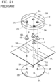
- JP 2018-129244 A discloses a connector as illustrated in FIG. 21 .
- the connector includes a housing 2 and a base member 3 that are disposed on the opposite sides of a flexible substrate 1 to sandwich the flexible substrate 1 therebetween.
- Tubular portions 4A of contacts 4 are passed through contact through-holes 2A of the housing 2, and flanges 4B of the contacts 4 are sandwiched between the housing 2 and conductors 1A exposed on a top surface of the flexible substrate 1.
- housing fixing posts 3B formed to project from the base member 3 are press-fitted into post accommodating portions 2B of the housing 2 as shown in FIG. 21 , so that the housing 2 and the base member 3 are fixed to each other.
- a wearable device When fitted to the connector disclosed in JP 2018-129244 A , a wearable device can be connected to electrodes constituted of the conductors.
- DE 10 2012 003865 A1 discloses an electrode formed by a riveted eyelet-and-stud, the male part of a snap fastener, thus making electrical contact with both sides of a piece of cloth comprising a conductive yarn.
- the present invention has been made to solve the foregoing problem and aims at providing a connector that enables to make an electrical connection of a contact to a conductor of a connection object regardless of whether the conductor is exposed on the top surface or the bottom surface of the connection object.
- the connector according to the invention comprises:
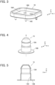
- FIG. 1 shows a connector 11 according to the embodiment.
- the connector 11 is, for instance, used as a garment-side connector for fitting a wearable device and has a housing 12 made of an insulating material.
- Four plug contacts 13 are retained in the housing 12, and a reinforcement sheet 14 and a sheet type conductive member 15 being superposed on each other are retained by the housing 12.
- the sheet type conductive member 15 constitutes a connection object to which the connector 11 is connected.
- the four plug contacts 13 are arranged in two rows parallel to each other and disposed to project perpendicularly to the sheet type conductive member 15.
- the reinforcement sheet 14 and the sheet type conductive member 15 are defined as extending in an XY plane, the arrangement direction of the four plug contacts 13 is referred to as "Y direction,” and the direction in which the four plug contacts 13 project is referred to as "+Z direction.”
- the Z direction is a fitting direction in which the connector 11 is fitted to a counter connector.
- FIG. 2 shows an exploded perspective view of the connector 11.
- the connector 11 includes a top insulator 16 and a bottom insulator 17, and these top and bottom insulators 16 and 17 constitute the housing 12.
- the four plug contacts 13 are retained in the top insulator 16.
- the reinforcement sheet 14 is disposed on the bottom surface, on the -Z direction side, of the top insulator 16, and the sheet type conductive member 15 is disposed on the -Z direction side of the reinforcement sheet 14.
- four inner contacts 18 are disposed on the -Z direction side of the sheet type conductive member 15, and the bottom insulator 17 is disposed on the -Z direction side of the inner contacts 18.
- the four inner contacts 18 separately correspond to the four plug contacts 13.
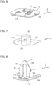
- the top insulator 16 includes a recessed portion 16A opening in the +Z direction and four contact through-holes 16B formed within the recessed portion 16A.
- the recessed portion 16A constitutes a counter connector accommodating portion in which part of a counter connector (not shown) is to be accommodated, and the four contact through-holes 16B correspond to the four plug contacts 13.
- the four plug contacts 13 are made of a conductive material such as metal, and are to be connected to corresponding contacts of a counter connector (not shown) when part of the counter connector is accommodated in the recessed portion 16A of the top insulator 16.
- the plug contact 13 has a tubular portion 13A in the shape of a cylindrical tube extending in the Z direction along the fitting axis C and a flange 13B extending along an XY plane from the -Z directional end of the tubular portion 13A.
- the tubular portion 13A is provided in its interior with a recessed portion 13C opening toward the -Z direction.
- the fitting axis C is an axis passing through the center of the tubular portion 13A and extending in the direction in which the connector 11 and the counter connector are fitted to each other.
- tubular portion 13A has the shape of a cylindrical tube, the cross section thereof is not limited to a circle and may be any of various shapes such as an ellipse and a polygon as long as the tubular portion 13A has the recessed portion 13C in its interior.
- the four plug contacts 13 can be each used as a terminal for transmitting electric signals.
- the bottom insulator 17 includes a flat plate portion 17A, and the flat plate portion 17A is provided with four recessed portions 17B opening in the +Z direction.
- the four recessed portions 17B correspond to the four plug contacts 13.
- the recessed portions 17B are separately provided with four projections 17C each projecting in the +Z direction from a center portion of the recessed portion 17B.
- the flat plate portion 17A is provided with a plurality of through-holes 17D corresponding to the bosses 16C of the top insulator 16.
- a bottom surface of the recessed portion 17B of the bottom insulator 17 constitutes a support surface 17E extending along an XY plane and facing in the +Z direction.
- the projection 17C is used to temporarily retain the inner contact 18 and includes a backrest surface 17F extending along a YZ plane and facing in the +X direction and a protrusion portion 17G projecting in the +X direction from a portion, situated at the center in the Y direction and on the -Z direction side, of the backrest surface 17F.
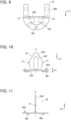
- the inner contact 18 is formed of a conductive metal plate being bent and includes a retaining portion 18A and a flat plate portion 18B connected to the -Z directional end of the retaining portion 18A.
- the retaining portion 18A is inserted into the recessed portion 13C of the corresponding plug contact 13, and the flat plate portion 18B is disposed on the support surface 17E of the corresponding recessed portion 17B of the bottom insulator 17.
- the retaining portion 18A has a flat plate shape extending along a YZ plane including the fitting axis C and is provided with a pair of contact point portions P1 separately at the +Y directional end and the -Y directional end of the retaining portion 18A, the contact point portions P1 being separated from each other in the Y direction.
- the retaining portion 18A is provided with a notch 18C extending in the -Z direction from a vicinity of the +Z directional end of the retaining portion 18A and opening toward the -Z direction.
- the protrusion portion 17G of the projection 17C of the bottom insulator 17 is fitted in the notch 18C of the retaining portion 18A.
- a distance in the Y direction between the pair of contact point portions P1 is designed to be slightly larger than an inner diameter of a part of the recessed portion 13C of the plug contact 13, with which part the contact point portions P1 make contact when the retaining portion 18A is inserted in the recessed portion 13C.
- the pair of contact point portions P1 make contact with an inner surface of the recessed portion 13C with a predetermined contact pressure while elastically displacing in a direction toward the fitting axis C.
- the flat plate portion 18B is a band plate-shaped member curving around the fixing axis C and extending along an XY plane.
- a plurality of top surface-side projections 18D are formed to project in the +Z direction
- a plurality of bottom surface-side projections 18E are formed to project in the -Z direction.
- the flat plate portion 18B has a U shape or a horseshoe shape extending as curving so as to encircle the retaining portion 18A, and the top surface side-projections 18D and the bottom surface-side projections 18E are alternately disposed in the direction in which the flat plate portion 18B extends.
- the +Z directional end of the top surface-side projection 18D is assumed to be separated from the -Z directional end of the bottom surface-side projection 18E by a distance D1 in the Z direction as shown in FIG. 10 .
- the sheet type conductive member 15 has a multilayer structure in which a plurality of wiring layers each formed of a conductor and a plurality of insulating layers are laminated.
- each contact arrangement region 15A used to arrange the four plug contacts 13 are defined on the top surface, facing the +Z direction, of the sheet type conductive member 15.
- a circular opening portion 15B through which the sheet type conductive member 15 is passed in the Z direction is formed, and around the opening portion 15B, a wiring layer 15C is exposed toward the +Z direction so as to surround the opening portion 15B.
- An insulating layer 15D is exposed in a region excluding the four contact arrangement regions 15A.
- the opening portion 15B penetrates the sheet type conductive member 15 in the Z direction, as shown in FIG. 13 , the opening portions 15B are also seen on the bottom surface of the sheet type conductive member 15 facing in the -Z direction at positions separately corresponding to the four contact arrangement regions 15A.
- a wiring layer 15E is exposed toward the -Z direction so as to surround the opening portions 15B separately formed at the positions corresponding to the four contact arrangement regions 15A, and an insulating layer 15F is exposed in the remaining region.
- the sheet type conductive member 15 is provided at its peripheral portion with a plurality of through-holes 15G corresponding to the bosses 16C of the top insulator 16, as shown in FIGS. 12 and 13 .
- the reinforcement sheet 14 is provided to reinforce a mounting object (not shown), such as a garment, on which the connector 11 is to be mounted.
- the reinforcement sheet 14 is made of an insulating material and provided at its center with an opening 14A. Further, a plurality of notches 14B corresponding to the bosses 16C of the top insulator 16 are formed along the periphery of the opening 14A of the reinforcement sheet 14.
- the four contact through-holes 16B of the top insulator 16, the four plug contacts 13, the four contact arrangement regions 15A of the sheet type conductive member 15, the four inner contacts 18, and the four recessed portions 17B of the bottom insulator 17 are arranged so as to align with one another in the Z direction.
- the bosses 16C of the top insulator 16, the notches 14B of the reinforcement sheet 14, the through-holes 15G of the sheet type conductive member 15, and the through-holes 17D of the bottom insulator 17 are arranged so as to align with one another in the Z direction.
- the inner contact 18 is temporarily retained by the projection 17C of the corresponding recessed portion 17B of the bottom insulator 17.
- the flat plate portion 18B of the inner contact 18 is inserted in the recessed portion 17B of the bottom insulator 17, and the protrusion portion 17G of the projection 17C of the bottom insulator 17 is fitted in the notch 18C of the retaining portion 18A, whereby the -X directional surface of the retaining portion 18A is brought into contact with the backrest surface 17F of the projection 17C.
- the bottom surface-side projections 18E formed on the bottom surface, facing in the -Z direction, of the flat plate portion 18B of the inner contact 18 are disposed on the support surface 17E of the recessed portion 17B of the bottom insulator 17.
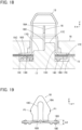
- tubular portions 13A of the plug contacts 13 are inserted correspondingly into the four contact through-holes 16B of the top insulator 16 from the -Z direction, and the bottom insulator 17 is pressed against the top insulator 16 in the +Z direction with the sheet type conductive member 15 being sandwiched therebetween.
- the retaining portion 18A of the inner contact 18 temporarily retained by the projection 17C of the bottom insulator 17 is inserted into the recessed portion 13C of the corresponding plug contact 13 via the opening portion 15B of the sheet type conductive member 15, the flange 13B of the plug contact 13 is positioned on the corresponding contact arrangement region 15A of the sheet type conductive member 15, and the sheet type conductive member 15 is sandwiched between the top surface-side projections 18D formed on the top surface, facing in the +Z direction, of the flat plate portion 18B of the inner contact 18 and the bottom surface on the -Z direction side of the flange 13B of the plug contact 13.
- the bosses 16C of the top insulator 16 sequentially pass through the notches 14B of the reinforcement sheet 14, the through-holes 15G of the sheet type conductive member 15, and the through-holes 17D of the bottom insulator 17. Then, the ends of the bosses 16C projecting on the -Z directional side of the bottom insulator 17 are heated and deformed, whereby the top insulator 16 and the bottom insulator 17 are fixed to each other as shown in FIG. 16 . Thus, the assembling operation of the connector 11 is completed.
- the top surface-side projections 18D formed on the top surface, facing in the +Z direction, of the flat plate portion 18B of the inner contact 18 receive pressing force acting in the -Z direction from the top insulator 16 via the flange 13B of the plug contact 13 and the sheet type conductive member 15.
- the bottom surface-side projections 18E formed on the bottom surface, facing in the -Z direction, of the flat plate portion 18B of the inner contact 18 are disposed on the support surface 17E of the recessed portion 17B of the bottom insulator 17, and hence due to the pressing force acting in the -Z direction on the top surface-side projections 18D, the flat plate portion 18B of the inner contact 18 elastically deforms such that the distance along the Z direction between the +Z directional end of the top surface-side projection 18D and the -Z directional end of the bottom surface-side projection 18E is narrowed.
- the flat plate portion 18B of the inner contact 18 Since in the flat plate portion 18B of the inner contact 18, the top surface-side projections 18D and the bottom surface-side projections 18E are alternately disposed along the direction in which the flat plate portion 18B extends, as shown in FIGS. 19 and 20 , the flat plate portion 18B elastically deforms wavily with respect to an XY plane, so that a distance D2 along the Z direction between the +Z directional end of the top surface-side projection 18D and the -Z directional end of the bottom surface-side projection 18E becomes narrower than the distance D1 shown in FIG. 10 .
- the top surface-side projections 18D are pressed against the bottom surface of the sheet type conductive member 15 in the +Z direction, and in addition, the top surface of the sheet type conductive member 15 is pressed against the bottom surface of the flange 13B of the plug contact 13 in the +Z direction.
- the wiring layer 15C is exposed around the opening portions 15B in the contact arrangement regions 15A on the top surface of the sheet type conductive member 15, and the wiring layer 15E is exposed around the opening portions 15B at the positions corresponding to the contact arrangement regions 15A on the bottom surface of the sheet type conductive member 15.
- the wiring layer 15C on the top surface of the sheet type conductive member 15 makes contact with the bottom surface of the flange 13B of the plug contact 13 with a predetermined contact pressure
- the wiring layer 15E on the bottom surface of the sheet type conductive member 15 makes contact with the top surface-side projections 18D of the inner contact 18 with a predetermined contact pressure
- the wiring layer 15C exposed on the top surface of the sheet type conductive member 15 is electrically connected to the plug contact 13 directly, and the wiring layer 15E exposed on the bottom surface of the sheet type conductive member 15 is electrically connected to the plug contact 13 via the inner contact 18.
- both the wiring layers 15C and 15E are connected to the plug contact 13.
- both the wiring layer 15C formed of a conductor and disposed on the top surface side of the sheet type conductive member 15 and the wiring layer 15E formed of a conductor and disposed on the bottom surface side of the same can be electrically connected to one plug contact 13 by use of the inner contact 18.
- the plug contact 13 can be electrically connected to the conductor on the top surface side of the sheet type conductive member, and when the connector 11 is connected to a sheet type conductive member having a conductor exposed only on the bottom surface side, the plug contact 13 can be electrically connected to the conductor on the bottom surface side of the sheet type conductive member.
- the plug contact 13 can be electrically connected to both the conductor on the top surface side and the conductor on the bottom surface side of the sheet type conductive member.
- the flat plate portion 18B of the inner contact 18 has a U shape or a horseshoe shape as shown in FIG. 9 , but the invention is not limited thereto, and the flat plate portion 18B may have a circular disc shape extending along an XY plane as with the flange 13B of the plug contact 13.
- the plug contact 13 disposed in the contact arrangement region 15A of the sheet type conductive member 15 is connected to both of the wiring layer 15C exposed on the top surface side of the sheet type conductive member 15 and the wiring layer 15E exposed on the bottom surface side of the sheet type conductive member 15, but the plug contact 13 disposed in the contact arrangement region 15A may be connected only to the wiring layer 15E exposed on the bottom surface side of the sheet type conductive member 15, for example.
- the sheet type conductive member 15 used in the embodiment described above has a multilayer structure, but the invention is not limited thereto, and it suffices if the sheet type conductive member 15 has a conductor exposed on at least one surface thereof.
- a double-layered conductor comprising the wiring layer 15C and the wiring layer 15E of the sheet type conductive member 15 is connected to one plug contact 13 in the embodiment described above, but the invention is not limited thereto, and a triple- or more-layered conductor may be connected to one plug contact 13.
- the connector 11 includes four plug contacts 13, the number of the plug contacts 13 is not limited thereto, and it suffices if at least the connector 11 includes one plug contact 13 to be electrically connected to a conductor exposed on at least one surface of the sheet type conductive member 15.
- the reinforcement sheet 14 is disposed between the bottom insulator 17 and the top insulator 16 in the embodiment described above, the reinforcement sheet 14 may be omitted when it is not necessary to reinforce a mounting object, such as a garment, on which the connector 11 is to be mounted.
Landscapes
- Coupling Device And Connection With Printed Circuit (AREA)
- Details Of Garments (AREA)
Claims (8)
- Verbinder, umfassend:einen Steckkontakt (13), der Leitfähigkeit besitzt und einen rohrförmigen Abschnitt (13A) und einen Flansch (13B) aufweist, wobei sich der rohrförmige Abschnitt entlang einer Montageachse (C) erstreckt und einen darin ausgebildeten vertieften Abschnitt (13C) aufweist, und wobei sich der Flansch von einem Endabschnitt des rohrförmigen Abschnitts in eine Richtung senkrecht zu der Montageachse erstreckt;einen unteren Isolator (17), der eine Stützfläche (17E) aufweist, die sich in der Richtung senkrecht zu der Montageachse erstreckt; undeinen inneren Kontakt (18), der Leitfähigkeit besitzt und auf der Stützfläche angeordnet ist, wobei ein Teil des inneren Kontakts in den vertieften Abschnitt eingesetzt ist,wobei der innere Kontakt (18) aufweist: einen Halteabschnitt (18A), der in dem vertieften Abschnitt gehalten ist und mit einer Innenfläche des vertieften Abschnitts in Kontakt steht, um elektrisch mit dem Steckkontakt verbunden zu sein; einen Flachplattenabschnitt (18B), der elastisch verformbar ist, mit dem Halteabschnitt verbunden ist, sich in der Richtung senkrecht zu der Montageachse erstreckt und einer Unterseite des Flansches zugewandt ist; mehrere obere-Oberfläche-seitige Vorsprünge (18D), die von einer oberen Oberfläche des Flachplattenabschnitts hin zu der Unterseite des Flansches vorstehen; und mehrere untere-Oberfläche-seitige Vorsprünge (18E), die von einer unteren Oberfläche des Flachplattenabschnitts getrennt an Positionen, die sich von Positionen der obere-Oberfläche-seitigen Vorsprünge unterscheiden, hin zu der Stützfläche vorstehen, undwobei ein Teil eines Verbindungsobjekts (15) vom Flachmaterialtyp, der einen Leiter (15C, 15E) aufweist, der an mindestens einer Fläche des Verbindungsobjekts frei liegt, in einer Richtung entlang der Montageachse zwischen der Unterseite des Flansches des Steckkontakts und den obere-Oberflächen-seitigen Vorsprüngen des inneren Kontakts sandwichartig aufgenommen ist, wobei die Unterseite des Flansches mit einer Oberseite des Verbindungsobjekts in Kontakt steht und die obere-Oberflächen-seitigen Vorsprünge in Kontakt mit einer Unterseite des Verbindungsobjekts stehen, wodurch der Steckkontakt (13) direkt mit dem Leiter (15C) elektrisch verbunden ist, wenn der Leiter an der Oberseite des Verbindungsobjekts frei liegt, und der Steckkontakt (13) über den inneren Kontakt (18) elektrisch mit dem Leiter (15E) verbunden ist, wenn der Leiter an der Unterseite des Verbindungsobjekts frei liegt.
- Verbinder nach Anspruch 1, wobei die obere-Oberfläche-seitigen Vorsprünge (18D) mit der Unterseite des Verbindungsobjekts (15) in Kontakt stehen und die untere-Oberfläche-seitigen Vorsprünge (18E) mit der Stützfläche (17E) in Kontakt stehen, wodurch sich der Flachplattenabschnitt (18B) elastisch so verformt, dass eine Distanz entlang der Montageachse zwischen den Spitzenenden der obere-Oberfläche-seitigen Vorsprünge (18D) und den Spitzenenden der untere-Oberfläche-seitigen Vorsprünge (18E) schmaler wird und die obere-Oberfläche-seitigen Vorsprünge die Unterseite des Verbindungsobjekts elastisch kontaktieren.
- Verbinder nach Anspruch 1 oder 2,wobei sich der Flachplattenabschnitt (18B) gekrümmt um die Montageachse (C) herum erstreckt unddie obere-Oberfläche-seitigen Vorsprünge (18D) und die untere-Oberfläche-seitigen Vorsprünge (18E) abwechselnd entlang einer Richtung angeordnet sind, in der sich der Flachplattenabschnitt erstreckt.
- Verbinder nach einem der Ansprüche 1-3, wobei der Halteabschnitt (18A) ein Paar von Kontaktpunktabschnitten (P1) aufweist, die in der Richtung senkrecht zu der Montageachse voneinander getrennt sind und mit der Innenfläche des vertieften Abschnitts in Kontakt stehen.
- Verbinder nach Anspruch 4, wobei der Halteabschnitt (18A) eine Flachplattenform aufweist, die sich entlang einer Ebene erstreckt, die die Montageachse (C) enthält.
- Verbinder nach Anspruch 5, wobei der untere Isolator (17) einen Vorsprung (17C) zum vorübergehenden Halten des inneren Kontakts (18) aufweist.
- Verbinder nach Anspruch 6,wobei der Halteabschnitt (18A) eine Ausnehmung (18C) aufweist, die sich hin zu der Stützfläche erstreckt, undder Vorsprung (17C) eine rückseitige Anliegefläche (17F), die sich entlang des Halteabschnitts erstreckt, und einen Vorsprungsabschnitt (17G), der von der rückseitigen Anliegefläche absteht und in die Ausnehmung eingepasst ist, aufweist.
- Verbinder nach einem der Ansprüche 1-7, umfassend einen oberen Isolator (16), der mit einem Kontaktdurchgangsloch (16B) versehen ist, durch das der rohrförmige Teil des Steckkontakts hindurchgeführt ist und das kleiner als der Flansch ist,
wobei der obere Isolator (16) an dem unteren Isolator (17) so befestigt ist, dass der rohrförmige Abschnitt des Steckkontakts durch das Kontaktdurchgangsloch hindurchgeführt ist und dass der Flansch des Steckkontakts, das Verbindungsobjekt und der Flachplattenabschnitt des inneren Kontakts zwischen dem oberen Isolator und dem unteren Isolator sandwichartig aufgenommen sind.
Applications Claiming Priority (1)
| Application Number | Priority Date | Filing Date | Title |
|---|---|---|---|
| JP2022154602A JP7822290B2 (ja) | 2022-09-28 | 2022-09-28 | コネクタ |
Publications (2)
| Publication Number | Publication Date |
|---|---|
| EP4346017A1 EP4346017A1 (de) | 2024-04-03 |
| EP4346017B1 true EP4346017B1 (de) | 2024-10-16 |
Family
ID=87567754
Family Applications (1)
| Application Number | Title | Priority Date | Filing Date |
|---|---|---|---|
| EP23190465.7A Active EP4346017B1 (de) | 2022-09-28 | 2023-08-09 | Verbinder |
Country Status (4)
| Country | Link |
|---|---|
| US (1) | US12456830B2 (de) |
| EP (1) | EP4346017B1 (de) |
| JP (1) | JP7822290B2 (de) |
| CN (1) | CN117791212A (de) |
Families Citing this family (3)
| Publication number | Priority date | Publication date | Assignee | Title |
|---|---|---|---|---|
| JP7822290B2 (ja) * | 2022-09-28 | 2026-03-02 | 日本航空電子工業株式会社 | コネクタ |
| JP2024094608A (ja) * | 2022-12-28 | 2024-07-10 | 日本航空電子工業株式会社 | コネクタおよび接続方法 |
| JP2025132682A (ja) * | 2024-02-29 | 2025-09-10 | 日本航空電子工業株式会社 | コネクタ |
Family Cites Families (20)
| Publication number | Priority date | Publication date | Assignee | Title |
|---|---|---|---|---|
| JPH0624143Y2 (ja) * | 1990-03-22 | 1994-06-22 | ソニーマグネスケール株式会社 | 同軸型コネクタの接続機構 |
| JP3119974U (ja) | 2005-10-17 | 2006-03-23 | 美那子 石井 | 草履を手編みするために用いる編み機である。 |
| JP2009199809A (ja) * | 2008-02-20 | 2009-09-03 | Mitsumi Electric Co Ltd | コネクタ、光伝送モジュールおよび光−電気伝送モジュール |
| DE102012003865A1 (de) * | 2012-02-22 | 2013-08-22 | Technische Universität Dresden | Einrichtung mit Anordnung zur Kontaktierung zwischen einem mit zumindest einer elektrisch leitfähigen Funktionsstruktur versehenen biegeweichen Materialstück und einem die Funktionsstruktur betreibenden Steuergerät |
| JP6840559B2 (ja) * | 2017-02-10 | 2021-03-10 | 日本航空電子工業株式会社 | コネクタ |
| JP6792493B2 (ja) * | 2017-03-17 | 2020-11-25 | 日本航空電子工業株式会社 | コネクタ |
| JP6942038B2 (ja) * | 2017-12-05 | 2021-09-29 | 日本航空電子工業株式会社 | コネクタ |
| JP7178956B2 (ja) * | 2019-05-17 | 2022-11-28 | 日本航空電子工業株式会社 | 接続方法、接続構造および接続端子組立体 |
| JP7232144B2 (ja) * | 2019-07-19 | 2023-03-02 | 日本航空電子工業株式会社 | コネクタ |
| JP7232143B2 (ja) * | 2019-07-19 | 2023-03-02 | 日本航空電子工業株式会社 | コネクタ |
| JP7196035B2 (ja) * | 2019-08-23 | 2022-12-26 | 日本航空電子工業株式会社 | コネクタおよび接続方法 |
| JP7313991B2 (ja) * | 2019-09-09 | 2023-07-25 | 日本航空電子工業株式会社 | コネクタ |
| JP7265458B2 (ja) * | 2019-09-26 | 2023-04-26 | 日本航空電子工業株式会社 | コネクタおよび接続方法 |
| JP7348060B2 (ja) * | 2019-10-03 | 2023-09-20 | 日本航空電子工業株式会社 | コネクタおよび接続方法 |
| US11258189B2 (en) * | 2019-10-03 | 2022-02-22 | Japan Aviation Electronics Industry, Limited | Connector and connecting method |
| JP7348024B2 (ja) * | 2019-10-24 | 2023-09-20 | 日本航空電子工業株式会社 | コネクタおよび接続方法 |
| JP7807994B2 (ja) * | 2022-06-27 | 2026-01-28 | 日本航空電子工業株式会社 | シート状導電部材およびコネクタ |
| JP2024041400A (ja) * | 2022-09-14 | 2024-03-27 | 日本航空電子工業株式会社 | コネクタ |
| JP7822290B2 (ja) * | 2022-09-28 | 2026-03-02 | 日本航空電子工業株式会社 | コネクタ |
| JP2024165753A (ja) * | 2023-05-18 | 2024-11-28 | 日本航空電子工業株式会社 | コネクタ、コネクタ組立体、接続構造および接続方法 |
-
2022
- 2022-09-28 JP JP2022154602A patent/JP7822290B2/ja active Active
-
2023
- 2023-07-06 US US18/347,966 patent/US12456830B2/en active Active
- 2023-08-02 CN CN202310966835.1A patent/CN117791212A/zh active Pending
- 2023-08-09 EP EP23190465.7A patent/EP4346017B1/de active Active
Also Published As
| Publication number | Publication date |
|---|---|
| CN117791212A (zh) | 2024-03-29 |
| US12456830B2 (en) | 2025-10-28 |
| JP2024048597A (ja) | 2024-04-09 |
| JP7822290B2 (ja) | 2026-03-02 |
| US20240106145A1 (en) | 2024-03-28 |
| EP4346017A1 (de) | 2024-04-03 |
Similar Documents
| Publication | Publication Date | Title |
|---|---|---|
| EP4346017B1 (de) | Verbinder | |
| US12424774B2 (en) | Connector | |
| EP4329104A1 (de) | Verbinder | |
| EP4300713B1 (de) | Blattartiges leitfähiges element und verbinder | |
| EP4395079B1 (de) | Verbinder und verbindungsverfahren | |
| EP4462605B1 (de) | Verbinder | |
| EP4318813B1 (de) | Verbinder | |
| EP4333215B1 (de) | Verbinder und verbinderanordnung | |
| EP4611180A1 (de) | Verbinder | |
| EP4507128B1 (de) | Verbinder und verbinderanordnung | |
| EP4333216B1 (de) | Verbinder | |
| JP2024021591A (ja) | コネクタ | |
| US12537336B2 (en) | Connector | |
| JP2024039795A (ja) | コネクタ |
Legal Events
| Date | Code | Title | Description |
|---|---|---|---|
| PUAI | Public reference made under article 153(3) epc to a published international application that has entered the european phase |
Free format text: ORIGINAL CODE: 0009012 |
|
| STAA | Information on the status of an ep patent application or granted ep patent |
Free format text: STATUS: REQUEST FOR EXAMINATION WAS MADE |
|
| 17P | Request for examination filed |
Effective date: 20230809 |
|
| AK | Designated contracting states |
Kind code of ref document: A1 Designated state(s): AL AT BE BG CH CY CZ DE DK EE ES FI FR GB GR HR HU IE IS IT LI LT LU LV MC ME MK MT NL NO PL PT RO RS SE SI SK SM TR |
|
| RBV | Designated contracting states (corrected) |
Designated state(s): AL AT BE BG CH CY CZ DE DK EE ES FI FR GB GR HR HU IE IS IT LI LT LU LV MC ME MK MT NL NO PL PT RO RS SE SI SK SM TR |
|
| GRAP | Despatch of communication of intention to grant a patent |
Free format text: ORIGINAL CODE: EPIDOSNIGR1 |
|
| STAA | Information on the status of an ep patent application or granted ep patent |
Free format text: STATUS: GRANT OF PATENT IS INTENDED |
|
| RIC1 | Information provided on ipc code assigned before grant |
Ipc: H05K 1/11 20060101ALN20240619BHEP Ipc: H01R 12/77 20110101ALI20240619BHEP Ipc: H01R 12/70 20110101ALI20240619BHEP Ipc: H01R 12/69 20110101ALI20240619BHEP Ipc: H05K 1/18 20060101ALI20240619BHEP Ipc: H01R 12/59 20110101AFI20240619BHEP |
|
| INTG | Intention to grant announced |
Effective date: 20240705 |
|
| GRAS | Grant fee paid |
Free format text: ORIGINAL CODE: EPIDOSNIGR3 |
|
| GRAA | (expected) grant |
Free format text: ORIGINAL CODE: 0009210 |
|
| STAA | Information on the status of an ep patent application or granted ep patent |
Free format text: STATUS: THE PATENT HAS BEEN GRANTED |
|
| AK | Designated contracting states |
Kind code of ref document: B1 Designated state(s): AL AT BE BG CH CY CZ DE DK EE ES FI FR GB GR HR HU IE IS IT LI LT LU LV MC ME MK MT NL NO PL PT RO RS SE SI SK SM TR |
|
| RAP3 | Party data changed (applicant data changed or rights of an application transferred) |
Owner name: JAPAN AVIATION ELECTRONICS INDUSTRY, LIMITED |
|
| REG | Reference to a national code |
Ref country code: GB Ref legal event code: FG4D |
|
| RAP4 | Party data changed (patent owner data changed or rights of a patent transferred) |
Owner name: JAPAN AVIATION ELECTRONICS INDUSTRY, LIMITED |
|
| REG | Reference to a national code |
Ref country code: CH Ref legal event code: EP Ref country code: DE Ref legal event code: R096 Ref document number: 602023000761 Country of ref document: DE |
|
| REG | Reference to a national code |
Ref country code: IE Ref legal event code: FG4D |
|
| REG | Reference to a national code |
Ref country code: LT Ref legal event code: MG9D |
|
| REG | Reference to a national code |
Ref country code: NL Ref legal event code: MP Effective date: 20241016 |
|
| REG | Reference to a national code |
Ref country code: AT Ref legal event code: MK05 Ref document number: 1733722 Country of ref document: AT Kind code of ref document: T Effective date: 20241016 |
|
| PG25 | Lapsed in a contracting state [announced via postgrant information from national office to epo] |
Ref country code: NL Free format text: LAPSE BECAUSE OF FAILURE TO SUBMIT A TRANSLATION OF THE DESCRIPTION OR TO PAY THE FEE WITHIN THE PRESCRIBED TIME-LIMIT Effective date: 20241016 |
|
| PG25 | Lapsed in a contracting state [announced via postgrant information from national office to epo] |
Ref country code: NL Free format text: LAPSE BECAUSE OF FAILURE TO SUBMIT A TRANSLATION OF THE DESCRIPTION OR TO PAY THE FEE WITHIN THE PRESCRIBED TIME-LIMIT Effective date: 20241016 |
|
| PG25 | Lapsed in a contracting state [announced via postgrant information from national office to epo] |
Ref country code: HR Free format text: LAPSE BECAUSE OF FAILURE TO SUBMIT A TRANSLATION OF THE DESCRIPTION OR TO PAY THE FEE WITHIN THE PRESCRIBED TIME-LIMIT Effective date: 20241016 Ref country code: IS Free format text: LAPSE BECAUSE OF FAILURE TO SUBMIT A TRANSLATION OF THE DESCRIPTION OR TO PAY THE FEE WITHIN THE PRESCRIBED TIME-LIMIT Effective date: 20250216 Ref country code: PT Free format text: LAPSE BECAUSE OF FAILURE TO SUBMIT A TRANSLATION OF THE DESCRIPTION OR TO PAY THE FEE WITHIN THE PRESCRIBED TIME-LIMIT Effective date: 20250217 |
|
| PG25 | Lapsed in a contracting state [announced via postgrant information from national office to epo] |
Ref country code: FI Free format text: LAPSE BECAUSE OF FAILURE TO SUBMIT A TRANSLATION OF THE DESCRIPTION OR TO PAY THE FEE WITHIN THE PRESCRIBED TIME-LIMIT Effective date: 20241016 |
|
| PG25 | Lapsed in a contracting state [announced via postgrant information from national office to epo] |
Ref country code: BG Free format text: LAPSE BECAUSE OF FAILURE TO SUBMIT A TRANSLATION OF THE DESCRIPTION OR TO PAY THE FEE WITHIN THE PRESCRIBED TIME-LIMIT Effective date: 20241016 |
|
| PG25 | Lapsed in a contracting state [announced via postgrant information from national office to epo] |
Ref country code: ES Free format text: LAPSE BECAUSE OF FAILURE TO SUBMIT A TRANSLATION OF THE DESCRIPTION OR TO PAY THE FEE WITHIN THE PRESCRIBED TIME-LIMIT Effective date: 20241016 |
|
| PG25 | Lapsed in a contracting state [announced via postgrant information from national office to epo] |
Ref country code: NO Free format text: LAPSE BECAUSE OF FAILURE TO SUBMIT A TRANSLATION OF THE DESCRIPTION OR TO PAY THE FEE WITHIN THE PRESCRIBED TIME-LIMIT Effective date: 20250116 |
|
| PG25 | Lapsed in a contracting state [announced via postgrant information from national office to epo] |
Ref country code: LV Free format text: LAPSE BECAUSE OF FAILURE TO SUBMIT A TRANSLATION OF THE DESCRIPTION OR TO PAY THE FEE WITHIN THE PRESCRIBED TIME-LIMIT Effective date: 20241016 Ref country code: AT Free format text: LAPSE BECAUSE OF FAILURE TO SUBMIT A TRANSLATION OF THE DESCRIPTION OR TO PAY THE FEE WITHIN THE PRESCRIBED TIME-LIMIT Effective date: 20241016 Ref country code: GR Free format text: LAPSE BECAUSE OF FAILURE TO SUBMIT A TRANSLATION OF THE DESCRIPTION OR TO PAY THE FEE WITHIN THE PRESCRIBED TIME-LIMIT Effective date: 20250117 |
|
| PG25 | Lapsed in a contracting state [announced via postgrant information from national office to epo] |
Ref country code: PL Free format text: LAPSE BECAUSE OF FAILURE TO SUBMIT A TRANSLATION OF THE DESCRIPTION OR TO PAY THE FEE WITHIN THE PRESCRIBED TIME-LIMIT Effective date: 20241016 |
|
| PG25 | Lapsed in a contracting state [announced via postgrant information from national office to epo] |
Ref country code: RS Free format text: LAPSE BECAUSE OF FAILURE TO SUBMIT A TRANSLATION OF THE DESCRIPTION OR TO PAY THE FEE WITHIN THE PRESCRIBED TIME-LIMIT Effective date: 20250116 |
|
| PG25 | Lapsed in a contracting state [announced via postgrant information from national office to epo] |
Ref country code: SM Free format text: LAPSE BECAUSE OF FAILURE TO SUBMIT A TRANSLATION OF THE DESCRIPTION OR TO PAY THE FEE WITHIN THE PRESCRIBED TIME-LIMIT Effective date: 20241016 |
|
| PG25 | Lapsed in a contracting state [announced via postgrant information from national office to epo] |
Ref country code: DK Free format text: LAPSE BECAUSE OF FAILURE TO SUBMIT A TRANSLATION OF THE DESCRIPTION OR TO PAY THE FEE WITHIN THE PRESCRIBED TIME-LIMIT Effective date: 20241016 |
|
| REG | Reference to a national code |
Ref country code: DE Ref legal event code: R097 Ref document number: 602023000761 Country of ref document: DE |
|
| PG25 | Lapsed in a contracting state [announced via postgrant information from national office to epo] |
Ref country code: EE Free format text: LAPSE BECAUSE OF FAILURE TO SUBMIT A TRANSLATION OF THE DESCRIPTION OR TO PAY THE FEE WITHIN THE PRESCRIBED TIME-LIMIT Effective date: 20241016 |
|
| PG25 | Lapsed in a contracting state [announced via postgrant information from national office to epo] |
Ref country code: RO Free format text: LAPSE BECAUSE OF FAILURE TO SUBMIT A TRANSLATION OF THE DESCRIPTION OR TO PAY THE FEE WITHIN THE PRESCRIBED TIME-LIMIT Effective date: 20241016 |
|
| PG25 | Lapsed in a contracting state [announced via postgrant information from national office to epo] |
Ref country code: SK Free format text: LAPSE BECAUSE OF FAILURE TO SUBMIT A TRANSLATION OF THE DESCRIPTION OR TO PAY THE FEE WITHIN THE PRESCRIBED TIME-LIMIT Effective date: 20241016 |
|
| PG25 | Lapsed in a contracting state [announced via postgrant information from national office to epo] |
Ref country code: CZ Free format text: LAPSE BECAUSE OF FAILURE TO SUBMIT A TRANSLATION OF THE DESCRIPTION OR TO PAY THE FEE WITHIN THE PRESCRIBED TIME-LIMIT Effective date: 20241016 |
|
| PG25 | Lapsed in a contracting state [announced via postgrant information from national office to epo] |
Ref country code: IT Free format text: LAPSE BECAUSE OF FAILURE TO SUBMIT A TRANSLATION OF THE DESCRIPTION OR TO PAY THE FEE WITHIN THE PRESCRIBED TIME-LIMIT Effective date: 20241016 |
|
| PLBE | No opposition filed within time limit |
Free format text: ORIGINAL CODE: 0009261 |
|
| STAA | Information on the status of an ep patent application or granted ep patent |
Free format text: STATUS: NO OPPOSITION FILED WITHIN TIME LIMIT |
|
| PG25 | Lapsed in a contracting state [announced via postgrant information from national office to epo] |
Ref country code: SE Free format text: LAPSE BECAUSE OF FAILURE TO SUBMIT A TRANSLATION OF THE DESCRIPTION OR TO PAY THE FEE WITHIN THE PRESCRIBED TIME-LIMIT Effective date: 20241016 |
|
| 26N | No opposition filed |
Effective date: 20250717 |
|
| PGFP | Annual fee paid to national office [announced via postgrant information from national office to epo] |
Ref country code: DE Payment date: 20250702 Year of fee payment: 3 |
|
| PGFP | Annual fee paid to national office [announced via postgrant information from national office to epo] |
Ref country code: FR Payment date: 20250703 Year of fee payment: 3 |