EP4333215B1 - Verbinder und verbinderanordnung - Google Patents
Verbinder und verbinderanordnung Download PDFInfo
- Publication number
- EP4333215B1 EP4333215B1 EP23185286.4A EP23185286A EP4333215B1 EP 4333215 B1 EP4333215 B1 EP 4333215B1 EP 23185286 A EP23185286 A EP 23185286A EP 4333215 B1 EP4333215 B1 EP 4333215B1
- Authority
- EP
- European Patent Office
- Prior art keywords
- contact
- recess
- connection target
- connector
- plug
- Prior art date
- Legal status (The legal status is an assumption and is not a legal conclusion. Google has not performed a legal analysis and makes no representation as to the accuracy of the status listed.)
- Active
Links
Images


Classifications
-
- H—ELECTRICITY
- H01—ELECTRIC ELEMENTS
- H01R—ELECTRICALLY-CONDUCTIVE CONNECTIONS; STRUCTURAL ASSOCIATIONS OF A PLURALITY OF MUTUALLY-INSULATED ELECTRICAL CONNECTING ELEMENTS; COUPLING DEVICES; CURRENT COLLECTORS
- H01R13/00—Details of coupling devices of the kinds covered by groups H01R12/70 or H01R24/00 - H01R33/00
- H01R13/02—Contact members
-
- H—ELECTRICITY
- H01—ELECTRIC ELEMENTS
- H01R—ELECTRICALLY-CONDUCTIVE CONNECTIONS; STRUCTURAL ASSOCIATIONS OF A PLURALITY OF MUTUALLY-INSULATED ELECTRICAL CONNECTING ELEMENTS; COUPLING DEVICES; CURRENT COLLECTORS
- H01R12/00—Structural associations of a plurality of mutually-insulated electrical connecting elements, specially adapted for printed circuits, e.g. printed circuit boards [PCB], flat or ribbon cables, or like generally planar structures, e.g. terminal strips, terminal blocks; Coupling devices specially adapted for printed circuits, flat or ribbon cables, or like generally planar structures; Terminals specially adapted for contact with, or insertion into, printed circuits, flat or ribbon cables, or like generally planar structures
- H01R12/50—Fixed connections
- H01R12/59—Fixed connections for flexible printed circuits, flat or ribbon cables or like structures
- H01R12/592—Fixed connections for flexible printed circuits, flat or ribbon cables or like structures connections to contact elements
-
- H—ELECTRICITY
- H01—ELECTRIC ELEMENTS
- H01R—ELECTRICALLY-CONDUCTIVE CONNECTIONS; STRUCTURAL ASSOCIATIONS OF A PLURALITY OF MUTUALLY-INSULATED ELECTRICAL CONNECTING ELEMENTS; COUPLING DEVICES; CURRENT COLLECTORS
- H01R12/00—Structural associations of a plurality of mutually-insulated electrical connecting elements, specially adapted for printed circuits, e.g. printed circuit boards [PCB], flat or ribbon cables, or like generally planar structures, e.g. terminal strips, terminal blocks; Coupling devices specially adapted for printed circuits, flat or ribbon cables, or like generally planar structures; Terminals specially adapted for contact with, or insertion into, printed circuits, flat or ribbon cables, or like generally planar structures
- H01R12/50—Fixed connections
- H01R12/59—Fixed connections for flexible printed circuits, flat or ribbon cables or like structures
- H01R12/65—Fixed connections for flexible printed circuits, flat or ribbon cables or like structures characterised by the terminal
-
- H—ELECTRICITY
- H01—ELECTRIC ELEMENTS
- H01R—ELECTRICALLY-CONDUCTIVE CONNECTIONS; STRUCTURAL ASSOCIATIONS OF A PLURALITY OF MUTUALLY-INSULATED ELECTRICAL CONNECTING ELEMENTS; COUPLING DEVICES; CURRENT COLLECTORS
- H01R12/00—Structural associations of a plurality of mutually-insulated electrical connecting elements, specially adapted for printed circuits, e.g. printed circuit boards [PCB], flat or ribbon cables, or like generally planar structures, e.g. terminal strips, terminal blocks; Coupling devices specially adapted for printed circuits, flat or ribbon cables, or like generally planar structures; Terminals specially adapted for contact with, or insertion into, printed circuits, flat or ribbon cables, or like generally planar structures
- H01R12/70—Coupling devices
- H01R12/7005—Guiding, mounting, polarizing or locking means; Extractors
- H01R12/7011—Locking or fixing a connector to a PCB
-
- H—ELECTRICITY
- H01—ELECTRIC ELEMENTS
- H01R—ELECTRICALLY-CONDUCTIVE CONNECTIONS; STRUCTURAL ASSOCIATIONS OF A PLURALITY OF MUTUALLY-INSULATED ELECTRICAL CONNECTING ELEMENTS; COUPLING DEVICES; CURRENT COLLECTORS
- H01R12/00—Structural associations of a plurality of mutually-insulated electrical connecting elements, specially adapted for printed circuits, e.g. printed circuit boards [PCB], flat or ribbon cables, or like generally planar structures, e.g. terminal strips, terminal blocks; Coupling devices specially adapted for printed circuits, flat or ribbon cables, or like generally planar structures; Terminals specially adapted for contact with, or insertion into, printed circuits, flat or ribbon cables, or like generally planar structures
- H01R12/70—Coupling devices
- H01R12/77—Coupling devices for flexible printed circuits, flat or ribbon cables or like structures
- H01R12/771—Details
- H01R12/774—Retainers
-
- H—ELECTRICITY
- H01—ELECTRIC ELEMENTS
- H01R—ELECTRICALLY-CONDUCTIVE CONNECTIONS; STRUCTURAL ASSOCIATIONS OF A PLURALITY OF MUTUALLY-INSULATED ELECTRICAL CONNECTING ELEMENTS; COUPLING DEVICES; CURRENT COLLECTORS
- H01R12/00—Structural associations of a plurality of mutually-insulated electrical connecting elements, specially adapted for printed circuits, e.g. printed circuit boards [PCB], flat or ribbon cables, or like generally planar structures, e.g. terminal strips, terminal blocks; Coupling devices specially adapted for printed circuits, flat or ribbon cables, or like generally planar structures; Terminals specially adapted for contact with, or insertion into, printed circuits, flat or ribbon cables, or like generally planar structures
- H01R12/70—Coupling devices
- H01R12/77—Coupling devices for flexible printed circuits, flat or ribbon cables or like structures
- H01R12/777—Coupling parts carrying pins, blades or analogous contacts
-
- H—ELECTRICITY
- H01—ELECTRIC ELEMENTS
- H01R—ELECTRICALLY-CONDUCTIVE CONNECTIONS; STRUCTURAL ASSOCIATIONS OF A PLURALITY OF MUTUALLY-INSULATED ELECTRICAL CONNECTING ELEMENTS; COUPLING DEVICES; CURRENT COLLECTORS
- H01R13/00—Details of coupling devices of the kinds covered by groups H01R12/70 or H01R24/00 - H01R33/00
- H01R13/02—Contact members
- H01R13/22—Contacts for co-operating by abutting
- H01R13/24—Contacts for co-operating by abutting resilient; resiliently-mounted
-
- H—ELECTRICITY
- H01—ELECTRIC ELEMENTS
- H01R—ELECTRICALLY-CONDUCTIVE CONNECTIONS; STRUCTURAL ASSOCIATIONS OF A PLURALITY OF MUTUALLY-INSULATED ELECTRICAL CONNECTING ELEMENTS; COUPLING DEVICES; CURRENT COLLECTORS
- H01R13/00—Details of coupling devices of the kinds covered by groups H01R12/70 or H01R24/00 - H01R33/00
- H01R13/62—Means for facilitating engagement or disengagement of coupling parts or for holding them in engagement
- H01R13/629—Additional means for facilitating engagement or disengagement of coupling parts, e.g. aligning or guiding means, levers, gas pressure electrical locking indicators, manufacturing tolerances
-
- H—ELECTRICITY
- H01—ELECTRIC ELEMENTS
- H01R—ELECTRICALLY-CONDUCTIVE CONNECTIONS; STRUCTURAL ASSOCIATIONS OF A PLURALITY OF MUTUALLY-INSULATED ELECTRICAL CONNECTING ELEMENTS; COUPLING DEVICES; CURRENT COLLECTORS
- H01R13/00—Details of coupling devices of the kinds covered by groups H01R12/70 or H01R24/00 - H01R33/00
- H01R13/648—Protective earth or shield arrangements on coupling devices, e.g. anti-static shielding
- H01R13/658—High frequency shielding arrangements, e.g. against EMI [Electro-Magnetic Interference] or EMP [Electro-Magnetic Pulse]
- H01R13/6591—Specific features or arrangements of connection of shield to conductive members
- H01R13/6597—Specific features or arrangements of connection of shield to conductive members the conductive member being a contact of the connector
-
- H—ELECTRICITY
- H01—ELECTRIC ELEMENTS
- H01R—ELECTRICALLY-CONDUCTIVE CONNECTIONS; STRUCTURAL ASSOCIATIONS OF A PLURALITY OF MUTUALLY-INSULATED ELECTRICAL CONNECTING ELEMENTS; COUPLING DEVICES; CURRENT COLLECTORS
- H01R2107/00—Four or more poles
Definitions
- the present invention relates to a connector, and relates particularly to a connector to be connected to a sheet-like connection target in which a flexible conductor is exposed on at least one surface.
- the present invention relates also to a connector assembly in which such a connector is attached to a connection target.
- the smart clothing includes an electrode placed at a measurement point, and can transmit biological information to a wearable device as a measurement instrument by electrically connecting the wearable device to the electrode.
- connection between the electrode and the wearable device can be made by, for example, using a connector to be connected to a flexible conductor drawn out from the electrode.
- JP 2018-129244 A discloses a connector like that shown in FIG. 20 .
- the connector includes a housing 2 and a base member 3 placed on both sides of a flexible board 1 with the flexible board 1 interposed therebetween; in the connector, a cylindrical portion 4A of a contact 4 is passed through a contact through hole 2A of the housing 2, and a flange 4B of the contact 4 is sandwiched between the housing 2 and a flexible conductor 1A exposed on a surface of the flexible board 1.
- a protrusion 3A of the base member 3 is inserted into a protrusion accommodating portion 4C of the contact 4 with the flexible substrate 1 interposed therebetween, and the inner surface of the protrusion accommodating portion 4C comes into contact with the flexible conductor 1A with a predetermined contact force, whereby the contact 4 is electrically connected to the flexible conductor 1A.
- housing fixing posts 3B formed to protrude on the base member 3 are press-fitted into post accommodating portions 2B of the housing 2, and thereby the housing 2 and the base member 3 are fixed to each other.
- the wearable device By fitting a wearable device to the connector disclosed in JP 2018-129244 A , the wearable device can be connected to an electrode made of a flexible conductor.
- EP 3 800 739 A1 discloses a connector and a connecting method.
- the connector includes a pushing member having a projection, a support member disposed to contact a lateral surface of the projection, and a contact made of a conductive material and having a support member facing portion facing the support member, a part of the flexible conductor being disposed between the support member and the support member facing portion of the contact, the lateral surface of the projection pressing the part of the flexible conductor against the support member facing portion of the contact via the support member, whereby the contact is electrically connected to the flexible conductor.
- the present invention has been made to solve such an existing problem, and an object of the present invention is to provide a connector and a connector assembly capable of electrically connecting a contact to a flexible conductor of a connection target regardless of whether the flexible conductor is exposed on the front surface or the back surface of the connection target.
- a connector according to the present invention is defined in claim 1 and comprises:
- the insertion portion includes the contact portion and the pressing portion that are formed in the same position in a direction along the fitting axis and, by part of the connection target being sandwiched between the pressing portion and the inner surface of the recess, the insertion portion is elastically deformed such that a spacing between the contact portion and the pressing portion is narrowed, and the contact portion elastically comes into contact with the inner surface of the recess, while the pressing portion elastically presses the part of the connection target toward the inner surface of the recess.
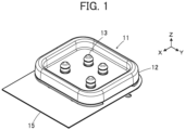
- FIG. 1 shows a connector assembly according to an embodiment.
- the connector assembly includes a connector 11.
- the connector 11 is used as, for example, a garment-side connector for fitting a wearable device, and includes a housing 12 made of an insulating material.
- Four plug contacts 13 are held in the housing 12, and a sheet-like conductive member 15 is held by the housing 12.
- the sheet-like conductive member 15 forms a connection target to which the connector 11 is connected, and the connector 11 and the sheet-like conductive member 15 constitute a connector assembly.
- the four plug contacts 13 are arranged in two rows parallel to each other in such a manner as to protrude perpendicularly to the sheet-like conductive member 15.
- the sheet-like conductive member 15 spreads along an XY plane, and the arrangement direction of the four plug contacts 13 is referred to as a Y direction and the direction in which the four plug contacts 13 protrude is referred to as a +Z direction.
- the Z direction is a fitting direction in which the connector 11 is fitted to the other-side connector.
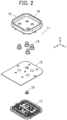
- FIG. 2 is an exploded perspective view of the connector assembly.
- the connector 11 includes a top insulator 16 and a bottom insulator 17, and the top insulator 16 and the bottom insulator 17 constitute the housing 12.
- the inner contact 18 corresponds to, among the four plug contacts 13, one plug contact 13 located on the -X direction side and the -Y direction side.
- the top insulator 16 and the bottom insulator 17, the four plug contacts 13, and the one inner contact 18 constitute the connector 11.
- the top insulator 16 has a recess 16A opened in the +Z direction and four contact through holes 16B formed in the recess 16A.
- the recess 16A constitutes an other-side connector accommodating portion in which part of a not-illustrated other-side connector is accommodated, and the four contact through holes 16B correspond to the four plug contacts 13.
- a plurality of bosses 16C protruding in the -Z direction are formed on the surface oriented in the -Z direction of the top insulator 16.
- the bottom insulator 17 has a flat plate portion 17A, and four circular recesses 17B opened in the +Z direction are formed in the flat plate portion 17A.
- the four recesses 17B correspond to the four plug contacts 13.
- An inner contact temporary holding unit 17C protruding in the +Z direction is formed in, among the four recesses 17B, one recess 17B located on the -X direction side and the -Y direction side, and three protrusions 17D protruding in the +Z direction are formed individually in the other three recesses 17B.
- a plurality of through holes 17E corresponding to the plurality of bosses 16C of the top insulator 16 are formed in the flat plate portion 17A.
- the inner contact temporary holding unit 17C formed in the recess 17B located on the -X direction side and the -Y direction side of the bottom insulator 17 has a columnar portion 17F extending in the Z direction and a pair of temporary holding pieces 17G protruding in the +X direction and the -X direction from an outer peripheral portion of the columnar portion 17F.
- the inner contact temporary holding unit 17C in a portion where the pair of temporary holding pieces 17G are formed, has a width W1 in the X direction.
- each of the protrusions 17D formed in the other three recesses 17B has a substantially regular hexagonal prism shape extending in the Z direction.
- Each of the four plug contacts 13 is formed of a conductive material such as metal, and is connected to the corresponding contact of the other-side connector when part of the not-illustrated other-side connector is accommodated in the recess 16A of the top insulator 16.
- the plug contact 13 has a cylindrical portion 13A in a circular cylindrical shape extending in the Z direction along a fitting axis C and a first flange 13B spreading along the XY plane from an end portion in the -Z direction of the cylindrical portion 13A.
- a recess 13C opened in the -Z direction is formed in the interior of the cylindrical portion 13A.
- the fitting axis C is an axis passing through the center of the cylindrical portion 13A and extending in the direction of fitting of the connector 11 and the other-side connector.
- the cylindrical portion 13A has a circular cylindrical shape
- the cross-sectional shape is not limited to a circular shape but may have various cross-sectional shapes such as an ellipse and a polygon as long as the cylindrical portion has the recess 13C in its interior.
- one plug contact 13 located on the -X direction side and the -Y direction side is connected to the ground potential and used as a shield terminal, and the other three plug contacts 13 are each used as a signal terminal for transmitting an electric signal.
- the sheet-like conductive member 15 has a sheet main body 15A made of an insulating material, and has a multilayer structure in which a signal wiring layer 15B formed of a flexible conductor, an insulating layer 15C, a shield layer 15D formed of a flexible conductor, and an insulating layer 15E are sequentially stacked on the front surface oriented in the +Z direction of the sheet main body 15A and a shield layer 15F formed of a flexible conductor and an insulating layer 15G are sequentially stacked on the back surface oriented in the -Z direction of the sheet main body 15A.
- four contact placement regions 15H for placing the four plug contacts 13 are defined on the surface oriented in the +Z direction of the sheet-like conductive member 15.
- one contact placement region 15H located on the -X direction side and the -Y direction side forms a region R1 where the plug contact 13 used as a shield terminal is placed, and the remaining three contact placement regions 15H each form a region R2 where the plug contact 13 used as a signal terminal is placed.
- the sheet-like conductive member 15 has a circular opening 15J formed in region R1.
- the opening 15J corresponds to the recess 13C of the plug contact 13, and penetrates the sheet-like conductive member 15 in the Z direction.
- the sheet-like conductive member 15 has a substantially rectangular protruding portion 15K protruding from an edge portion of the opening 15J into the opening 15J.
- the signal wiring layer 15B is exposed in the +Z direction by removing the insulating layer 15E, the shield layer 15D, and the insulating layer 15C.
- the insulating layer 15E is exposed in the region other than regions R1 and R2.
- a plurality of through holes 15L corresponding to the plurality of bosses 16C of the top insulator 16 are formed in a peripheral edge portion of the sheet-like conductive member 15.
- the protruding portion 15K in region R1 protrudes in the - Y direction from an edge portion on the +Y direction side of the opening 15J into the opening 15J, and in the protruding portion 15K, the shield layer 15D is exposed in the +Z direction by removing the insulating layer 15E.
- the opening 15J penetrates the sheet-like conductive member 15 in the Z direction, as shown in FIG. 13 , the opening 15J and the protruding portion 15K are seen in a position corresponding to region R1 also on the back surface oriented in the -Z direction of the sheet-like conductive member 15.
- the insulating layer 15G is exposed in the region other than the position corresponding to region R1. Further, as shown in FIG. 14 , in the protruding portion 15K, the shield layer 15F is exposed in the -Z direction by removing the insulating layer 15G.
- FIGS. 15 and 16 show a configuration of the inner contact 18.
- the inner contact 18 is formed of a conductive material such as metal, and has a cylindrical, elastically deformable insertion portion 18A through which the fitting axis C passes and a second flange 18B spreading along the XY plane from an end portion in the -Z direction of the insertion portion 18A.
- the insertion portion 18A is to be inserted into the recess 13C of the plug contact 13 through the opening 15J in region R1 of the sheet-like conductive member 15, and has a large-diameter portion 18C placed on the -Z direction side and a small-diameter portion 18D joined to the +Z direction side of the large-diameter portion 18C.
- Each of the large-diameter portion 18C and the small-diameter portion 18D has a circular cylindrical shape with the center at the fitting axis C, and the small-diameter portion 18D has a diameter smaller than the large-diameter portion 18C.
- the inner diameter D1 of the small-diameter portion 18D is formed slightly smaller than the width W1 in the X direction of the inner contact temporary holding unit 17C in a portion of the bottom insulator 17 where the pair of temporary holding pieces 17G are formed as shown in FIG. 6 .
- the pair of temporary holding pieces 17G of the inner contact temporary holding unit 17C are fitted to the interior of the small-diameter portion 18D, and the inner contact 18 can be temporarily held on the inner contact temporary holding unit 17C.
- a contact portion P1 and a pressing portion P2 placed on opposite sides across the fitting axis C are formed on the outer peripheral surface of the large-diameter portion 18C.
- the contact portion P1 and the pressing portion P2 are placed in substantially the same position in the Z direction along the fitting axis C; the contact portion P1 is located on the -Y direction side, and the pressing portion P2 is located on the +Y direction side.
- the spacing in the Y direction between the contact portion P1 and the pressing portion P2, that is, the outer diameter D2 of the large-diameter portion 18C is set slightly larger than a value obtained by subtracting the thickness of the sheet-like conductive member 15 from the inner diameter of a portion of the recess 13C with which the contact portion P1 and the pressing portion P2 come into contact when the inner contact 18 is inserted into the recess 13C of the plug contact 13.
- the inner diameter of the large-diameter portion 18C is formed larger than the diameter or the width in the X direction of any portion of the inner contact temporary holding unit 17C.
- the protruding portion 15K in region R1 of the sheet-like conductive member 15 protrudes in the -Y direction from an edge portion on the +Y direction side of the opening 15J. Therefore, when the inner contact 18 is inserted into the recess 13C of the plug contact 13 through the opening 15J of the sheet-like conductive member 15, the protruding portion 15K is pushed into the recess 13C by the inner contact 18 and sandwiched between the pressing portion P2 formed on the +Y direction side of the large-diameter portion 18C and the inner surface on the +Y direction side of the recess 13C, and the contact portion P1 formed on the -Y direction side of the large-diameter portion 18C comes into contact with the inner surface on the - Y direction side of the recess 13C.
- the spacing in the Y direction between the contact portion P1 and the pressing portion P2 is set slightly larger than a value obtained by subtracting the thickness of the sheet-like conductive member 15 from the inner diameter of a portion of the recess 13C with which the contact portion P1 and the pressing portion P2 come into contact when the inner contact 18 is inserted into the recess 13C of the plug contact 13, each of the contact portion P1 and the pressing portion P2 receives a force F1 in the Y direction from the inner surface of the recess 13C toward the fitting axis C, and as indicated by the broken line in FIG. 16 , the insertion portion 18A of the inner contact 18 is elastically deformed such that the spacing in the Y direction between the contact portion P1 and the pressing portion P2 is narrowed.
- each of the large-diameter portion 18C and the small-diameter portion 18D of the insertion portion 18A has a circular cylindrical shape with the center at the fitting axis C
- the shape is not limited to a circular cylindrical shape, and may be any shape as long as it is, for example, a cylindrical shape having any of various cross-sectional shapes such as an ellipse and a polygon.
- the four contact through holes 16B of the top insulator 16, the four plug contacts 13, the four contact placement regions 15H of the sheet-like conductive member 15, and the four recesses 17B of the bottom insulator 17 are placed in positions aligned with each other in the Z direction.
- the inner contact 18 is placed in a position aligned in the Z direction with, among the four contact placement regions 15H of the sheet-like conductive member 15, the contact placement region 15H forming region R1 and located on the -X direction side and the -Y direction side and, among the four recesses 17B of the bottom insulator 17, the recess 17B located on the -X direction side and the -Y direction side where the inner contact temporary holding unit 17C is formed.
- the plurality of bosses 16C of the top insulator 16, the plurality of through holes 15L of the sheet-like conductive member 15, and the plurality of through holes 17E of the bottom insulator 17 are placed in positions aligned with each other in the Z direction.
- each plug contact 13 is inserted from the -Z direction into the corresponding one of the four contact through holes 16B of the top insulator 16, and the sheet-like conductive member 15 is placed on the -Z direction side of the four plug contacts 13. At this time, the sheet-like conductive member 15 is placed such that the four contact placement regions 15H come into contact with the first flanges 13B of the four plug contacts 13.
- the insertion portion 18A of the inner contact 18 is put on the inner contact temporary holding unit 17C of the bottom insulator 17, and thereby the inner contact 18 is temporarily held on the inner contact temporary holding unit 17C.
- the insertion portion 18A of the inner contact 18 temporarily held on the inner contact temporary holding unit 17C of the bottom insulator 17 is inserted into the recess 13C of the plug contact 13 through the opening 15J while pushing the protruding portion 15K of the sheet-like conductive member 15 until the sheet-like conductive member 15 is sandwiched between the first flange 13B of the plug contact 13 and the second flange 18B of the inner contact 18.
- the three protrusions 17D of the bottom insulator 17 are inserted individually into the recesses 13C of the corresponding plug contacts 13 while pushing regions R2 of the sheet-like conductive member 15.
- region R2 of the sheet-like conductive member 15 is inserted into the recess 13C of the plug contact 13 while expanding due to the protrusion 17D of the bottom insulator 17; if the stretchability of the sheet-like conductive member 15 is not sufficient, it is desirable that a plurality of notches penetrating the sheet-like conductive member 15 in the Z direction be formed in each region R2 in advance. With this configuration, the protrusion 17D is inserted into the recess 13C of the plug contact 13 while opening the plurality of notches in region R2.
- the plurality of bosses 16C of the top insulator 16 sequentially penetrate the plurality of through holes 15L of the sheet-like conductive member 15 and the plurality of through holes 17E of the bottom insulator 17. Then, as shown in FIG. 17 , the distal ends of the plurality of bosses 16C protruding on the -Z direction side of the bottom insulator 17 are thermally deformed, and thereby the top insulator 16 and the bottom insulator 17 are fixed to each other; thus, the assembly of the connector assembly is completed.
- Each plug contact 13 is fixed to the top insulator 16 and the bottom insulator 17 by the first flange 13B being sandwiched between the top insulator 16 and the bottom insulator 17.
- the insertion portion 18A of the inner contact 18 is inserted into the recess 13C of the plug contact 13 while pushing the protruding portion 15K of the sheet-like conductive member 15. Consequently, the sheet-like conductive member 15 is sandwiched between the first flange 13B of the plug contact 13 and the second flange 18B of the inner contact 18.
- the protruding portion 15K protruding in the -Y direction from an edge portion on the +Y direction side of the opening 15J of the sheet-like conductive member 15 is sandwiched between the pressing portion P2 formed on the +Y direction side of the inner contact 18 and the inner surface on the +Y direction side of the recess 13C, and the contact portion P1 formed on the -Y direction side of the inner contact 18 comes into contact with the inner surface on the -Y direction side of the recess 13C.
- the insertion portion 18A of the inner contact 18 is elastically deformed such that the spacing in the Y direction between the contact portion P1 and the pressing portion P2 is narrowed, and the contact portion P1 of the inner contact 18 elastically comes into contact with the inner surface on the -Y direction side of the recess 13C of the plug contact 13; thus, the inner contact 18 is electrically connected to the plug contact 13.
- the protruding portion 15K of the sheet-like conductive member 15 sandwiched between the pressing portion P2 of the inner contact 18 and the inner surface on the +Y direction side of the recess 13C of the plug contact 13 is elastically pressed toward the inner surface on the +Y direction side of the recess 13C of the plug contact 13 by the pressing portion P2.
- the shield layer 15D is exposed on the front surface side of the sheet-like conductive member 15, and the shield layer 15F is exposed on the back surface side of the sheet-like conductive member 15.
- the shield layer 15D on the front surface side of the protruding portion 15K comes into contact with the inner surface on the +Y direction side of the recess 13C of the plug contact 13 with a predetermined contact pressure
- the shield layer 15F on the back surface side of the protruding portion 15K comes into contact with the pressing portion P2 of the inner contact 18 with a predetermined contact pressure.
- the shield layer 15D exposed on the front surface of the protruding portion 15K of the sheet-like conductive member 15 is directly electrically connected to the plug contact 13
- the shield layer 15F exposed on the back surface of the protruding portion 15K is electrically connected to the plug contact 13 via the inner contact 18. That is, both the shield layers 15D and 15F are connected to the plug contact 13 used as a shield terminal.
- both the shield layer 15D placed on the front surface side of the protruding portion 15K of the sheet-like conductive member 15 and the shield layer 15F placed on the back surface side can be electrically connected to one plug contact 13 placed in region R1.
- each protrusion 17D of the bottom insulator 17 is inserted into the recess 13C of the plug contact 13 as shown in FIG. 19 .
- the sheet-like conductive member 15 is sandwiched between the side surface of the protrusion 17D and the inner surface of the recess 13C of the plug contact 13, and the signal wiring layer 15B comes into contact with the inner surface of the recess 13C of the plug contact 13 with a predetermined contact pressure and is electrically connected to the plug contact 13 placed in region R2.
- the signal wiring layer 15B has been subjected to predetermined patterning, and three wiring lines formed of the signal wiring layer 15B and insulated from each other are connected individually to the three plug contacts 13 placed in the three regions R2.
- the signal wiring layer 15B is stacked between the shield layer 15D placed on the front surface side of the sheet-like conductive member 15 and the shield layer 15F placed on the back surface side in a state of being insulated from these shield layers 15D and 15F; therefore, a shielding effect on the signal wiring layer 15B is exerted by connecting the plug contact 13 placed in region R1 and connected to the shield layer 15D and the shield layer 15F to the ground potential, and high-accuracy signal transmission in which the influence of disturbance due to electromagnetic waves or the like is suppressed can be performed.
- the contact portion P1 and the pressing portion P2 are each shown as a point on the outer peripheral surface of the large-diameter portion 18C of the inner contact 18, a contact portion P1 and a pressing portion P2 extending linearly along the Z direction can be set because the large-diameter portion 18C has a circular cylindrical shape with the center at the fitting axis C.
- the protruding portion 15K of the sheet-like conductive member 15 has a substantially rectangular shape protruding from an edge portion of the opening 15J into the opening 15J
- the shape of the protruding portion is not limited to the shape of the protruding portion 15K as long as the protruding portion is one that, when the insertion portion 18A of the inner contact 18 is being inserted into the recess 13C of the plug contact 13, is pushed into the recess 13C together with the insertion portion 18A and is sandwiched between the pressing portion P2 of the insertion portion 18A and the inner surface of the recess 13C.
- the sheet-like conductive member 15 has one protruding portion 15K protruding into the opening 15J
- the number of protruding portions 15K is not limited to one, and also a configuration is possible in which two or more protruding portions 15K protrude from an edge portion of the opening 15J into the opening 15J and these two or more protruding portions 15K are sandwiched between the pressing portion P2 of the insertion portion 18A and the inner surface of the recess 13C.
- the bottom insulator 17 is pressed toward the top insulator 16 after the inner contact 18 is temporarily held on the inner contact temporary holding unit 17C of the bottom insulator 17; however, it is not always necessary to temporarily hold the inner contact 18 on the inner contact temporary holding unit 17C.
- the cylindrical portions 13A of the plug contacts 13 are inserted into the corresponding four contact through holes 16B of the top insulator 16, and the sheet-like conductive member 15 is placed on the -Z direction side of the four plug contacts 13; in this state, the insertion portion 18A of the inner contact 18 is inserted into the recess 13C of the plug contact 13 placed in region R1 of the sheet-like conductive member 15 while pushing the protruding portion 15K, and then the bottom insulator 17 is pressed toward the top insulator 16.
- the inner contact temporary holding unit 17C of the bottom insulator 17 becomes unnecessary.
- the plug contact 13 placed in region R1 of the sheet-like conductive member 15 is connected to both the shield layer 15D exposed on the front surface side of the sheet-like conductive member 15 and the shield layer 15F exposed on the back surface side of the sheet-like conductive member 15; however, for example, also a configuration is possible in which only the shield layer 15F exposed on the back surface side of the sheet-like conductive member 15 is connected to the plug contact 13 placed in region R1.
- the sheet-like conductive member 15 used in the above embodiment has the multilayer structure shown in FIG. 10
- the sheet-like conductive member is not limited thereto, and may have any structure as long as it has at least a flexible conductor placed on at least one surface of the sheet main body.
- the two conductive layers of the shield layer 15D and the shield layer 15F of the sheet-like conductive member 15 are connected to one plug contact 13 used as a shield terminal, the configuration is not limited thereto, and three or more conductive layers may be connected to one plug contact 13.
- the connector 11 in the above embodiment includes four plug contacts 13 including a contact used as a shield terminal and a contact used as a signal terminal
- the configuration is not limited to this number of plug contacts 13, and may be any configuration as long as it includes at least one plug contact 13 to be electrically connected to a flexible conductor placed on the front surface side or the back surface side of the sheet main body of the sheet-like conductive member 15.
- a not-illustrated reinforcing sheet made of an insulating material may be placed between the top insulator 16 and the sheet-like conductive member 15.
- the reinforcing sheet has an opening formed at the center, and the four plug contacts 13 are inserted into the four contact through holes 16B of the top insulator 16 through the opening.
Landscapes
- Coupling Device And Connection With Printed Circuit (AREA)
- Slide Fasteners, Snap Fasteners, And Hook Fasteners (AREA)
Claims (7)
- Verbinder, umfassend:einen Steckkontakt (13) in einer zylindrischen Form, der Leitfähigkeit besitzt und eine Aussparung (13C) aufweist, die sich entlang einer Montageachse (C) erstreckt; undeinen inneren Kontakt (18), der Leitfähigkeit besitzt und einen Einführungsabschnitt (18A) in einer zylindrischen Form aufweist, der elastisch verformbar ist, der in die Aussparung eingeführt ist und durch den hindurch die Montageachse verläuft,wobei der Einführungsabschnitt aufweist: einen Kontaktabschnitt (P1), der an einer Außenumfangsfläche des Einführungsabschnitts platziert ist und der mit dem Steckkontakt in der Aussparung in Kontakt kommt; und einen Drückabschnitt (P2), der an der Außenumfangsfläche des Einführungsabschnitts und auf einer dem Kontaktabschnitt gegenüberliegenden Seite quer zu der Montageachse platziert ist, undein Teil eines flachmaterialartigen Verbindungsziels (15), das einen flexiblen Leiter (15B, 15D, 15F) aufweist, der an mindestens einer Fläche frei liegt, zwischen dem Drückabschnitt und einer Innenfläche der Aussparung in einer Richtung orthogonal zu der Montageachse sandwichartig aufgenommen ist, die Innenfläche der Aussparung mit einer Vorderseite des Verbindungsziels in Kontakt kommt und der Drückabschnitt mit einer Rückseite des Verbindungsziels in Kontakt kommt, wodurch der Steckkontakt in einem Fall, in dem der flexible Leiter an der Vorderseite des Verbindungsziels frei liegt, direkt elektrisch mit dem flexiblen Leiter verbunden ist, und der Steckkontakt in einem Fall, in dem der flexible Leiter an der Rückseite des Verbindungsziels frei liegt, über den inneren Kontakt elektrisch mit dem flexiblen Leiter verbunden ist,der Einführungsabschnitt (18A) den Kontaktabschnitt (P1) und den Drückabschnitt (P2) aufweist, die in derselben Position in einer Richtung entlang der Montageachse gebildet sind,dadurch gekennzeichnet, dass:
indem ein Teil des Verbindungsziels (15) zwischen dem Drückabschnitt und der Innenfläche der Aussparung sandwichartig angeordnet ist, der Einführungsabschnitt (18A) elastisch so verformt ist, dass ein Abstand zwischen dem Kontaktabschnitt und dem Drückabschnitt verschmälert ist, und der Kontaktabschnitt (P1) elastisch mit der Innenfläche der Aussparung in Kontakt kommt, während der Drückabschnitt (P2) den Teil des Verbindungsziels elastisch in Richtung der Innenfläche der Aussparung drückt. - Verbinder nach Anspruch 1,wobei der Steckkontakt (13) einen zylindrischen Abschnitt (13A) und einen ersten Flansch (13B), der an einem Ende des zylindrischen Abschnitts gebildet ist, aufweist,der innere Kontakt (18) einen zweiten Flansch (18B) aufweist, der an einem Ende des Einführungsabschnitts gebildet und so platziert ist, dass er mit dem ersten Flansch gestapelt ist,die Aussparung (13C) von einem Inneren des zylindrischen Abschnitts gebildet ist unddas Verbindungsziel (15) zwischen dem ersten Flansch und dem zweiten Flansch sandwichartig angeordnet ist.
- Verbinder nach Anspruch 2, aufweisend ein Gehäuse (12), das eine isolierende Eigenschaft besitzt und dazu eingerichtet ist, das Verbindungsziel (15), den Steckkontakt (13) und den inneren Kontakt (18) zu halten,
wobei das Gehäuse aufweist:einen oberen Isolator (16), der mit einem Kontaktdurchgangsloch (16B) versehen ist, durch das hindurch sich der zylindrische Abschnitt des Steckkontakts erstreckt und das kleiner als der erste Flansch (13B) ist; undeinen unteren Isolator (17), undder obere Isolator ist so an dem unteren Isolator befestigt, dass der zylindrische Abschnitt des Steckkontakts durch das Kontaktdurchgangsloch hindurch führt und dass das Verbindungsziel, der erste Flansch und der zweite Flansch zwischen dem oberen Isolator und dem unteren Isolator sandwichartig angeordnet sind. - Verbinder nach Anspruch 3, wobei der untere Isolator (17) eine Einheit (17C) zum temporären Halten des inneren Kontakts aufweist, die in das Innere des Einführungsabschnitts des inneren Kontakts (18) eingeführt ist und die den inneren Kontakt temporär hält.
- Verbinder nach Anspruch 4,wobei die Einheit (17C) zum temporären Halten des inneren Kontakts aufweist: einen säulenförmigen Abschnitt (17F), der sich entlang der Montageachse erstreckt; und ein Paar temporärer Haltestücke (17G), die von einem Außenumfangsabschnitt des säulenförmigen Abschnitts in einer Richtung vorstehen, die orthogonal zu der Montageachse verläuft und die orthogonal zu dem Kontaktabschnitt und zu dem Drückabschnitt um die Montageachse verläuft, undder innere Kontakt temporär an dem unteren Isolator gehalten ist, indem der Einführungsabschnitt an die Einheit zum temporären Halten des inneren Kontakts gesetzt ist.
- Verbinder nach Anspruch 5,wobei der Einführungsabschnitt (18A) des inneren Kontakts (18) aufweist: einen Abschnitt (18C) mit großem Durchmesser, der eine kreiszylindrische Form mit einer Mitte an der Montageachse aufweist; und einen Abschnitt (18D) mit kleinem Durchmesser, der mit dem Abschnitt mit großem Durchmesser verbunden ist und eine kreiszylindrische Form mit einer Mitte an der Montageachse aufweist,der innere Kontakt temporär an dem unteren Isolator gehalten ist, indem das Paar temporärer Haltestücke an einem Inneren des Abschnitts mit kleinem Durchmesser angebracht ist, undder Kontaktabschnitt und der Drückabschnitt an einer Außenumfangsfläche des Abschnitts mit großem Durchmesser platziert sind.
- Verbinderanordnung, aufweisend:das Verbindungsziel (15); undden Verbinder (11) nach einem der Ansprüche 1-6, der mit dem Verbindungsziel verbunden ist,wobei das Verbindungsziel (15) aufweist: eine Öffnung (15J) korrespondierend zu der Aussparung des Steckkontakts; und einen vorstehenden Abschnitt (15K), der von einem Randabschnitt der Öffnung in die Öffnung hinein vorsteht, undder Einführungsabschnitt durch die Öffnung in die Aussparung eingeführt ist, während er gegen den vorstehenden Abschnitt drückt, und der vorstehende Abschnitt, als Teil des Verbindungsziels, zwischen dem Drückabschnitt und einer Innenfläche der Aussparung sandwichartig angeordnet ist.
Applications Claiming Priority (1)
| Application Number | Priority Date | Filing Date | Title |
|---|---|---|---|
| JP2022137646A JP2024033809A (ja) | 2022-08-31 | 2022-08-31 | コネクタおよびコネクタ組立体 |
Publications (2)
| Publication Number | Publication Date |
|---|---|
| EP4333215A1 EP4333215A1 (de) | 2024-03-06 |
| EP4333215B1 true EP4333215B1 (de) | 2025-01-15 |
Family
ID=87280899
Family Applications (1)
| Application Number | Title | Priority Date | Filing Date |
|---|---|---|---|
| EP23185286.4A Active EP4333215B1 (de) | 2022-08-31 | 2023-07-13 | Verbinder und verbinderanordnung |
Country Status (4)
| Country | Link |
|---|---|
| US (1) | US12525733B2 (de) |
| EP (1) | EP4333215B1 (de) |
| JP (1) | JP2024033809A (de) |
| CN (1) | CN117638542A (de) |
Families Citing this family (1)
| Publication number | Priority date | Publication date | Assignee | Title |
|---|---|---|---|---|
| JP2024041400A (ja) * | 2022-09-14 | 2024-03-27 | 日本航空電子工業株式会社 | コネクタ |
Family Cites Families (14)
| Publication number | Priority date | Publication date | Assignee | Title |
|---|---|---|---|---|
| DE3918375A1 (de) * | 1989-06-06 | 1990-12-13 | Prym Werke William | Druckknopfverbindung |
| US5562607A (en) * | 1995-01-18 | 1996-10-08 | Alza Corporation | Electrotransport device having reusable controller power saver |
| JP6840559B2 (ja) * | 2017-02-10 | 2021-03-10 | 日本航空電子工業株式会社 | コネクタ |
| JP6792493B2 (ja) * | 2017-03-17 | 2020-11-25 | 日本航空電子工業株式会社 | コネクタ |
| SE542380C2 (en) * | 2018-07-16 | 2020-04-21 | Inuheat Group Ab | Electrical connector |
| JP7178956B2 (ja) * | 2019-05-17 | 2022-11-28 | 日本航空電子工業株式会社 | 接続方法、接続構造および接続端子組立体 |
| JP7232143B2 (ja) * | 2019-07-19 | 2023-03-02 | 日本航空電子工業株式会社 | コネクタ |
| JP7313990B2 (ja) * | 2019-09-09 | 2023-07-25 | 日本航空電子工業株式会社 | コネクタおよび接続方法 |
| JP7348016B2 (ja) * | 2019-10-01 | 2023-09-20 | 日本航空電子工業株式会社 | コネクタ |
| US11258189B2 (en) | 2019-10-03 | 2022-02-22 | Japan Aviation Electronics Industry, Limited | Connector and connecting method |
| JP7348060B2 (ja) * | 2019-10-03 | 2023-09-20 | 日本航空電子工業株式会社 | コネクタおよび接続方法 |
| JP7348024B2 (ja) * | 2019-10-24 | 2023-09-20 | 日本航空電子工業株式会社 | コネクタおよび接続方法 |
| CN111029815B (zh) * | 2019-12-27 | 2021-10-26 | 上海创功通讯技术有限公司 | Fpc连接器及fpc连接组件 |
| FI20206359A1 (en) * | 2020-12-22 | 2022-06-23 | Suunto Oy | Female snap connectors and associated devices and methods |
-
2022
- 2022-08-31 JP JP2022137646A patent/JP2024033809A/ja active Pending
-
2023
- 2023-06-30 CN CN202310800164.1A patent/CN117638542A/zh active Pending
- 2023-07-12 US US18/350,984 patent/US12525733B2/en active Active
- 2023-07-13 EP EP23185286.4A patent/EP4333215B1/de active Active
Also Published As
| Publication number | Publication date |
|---|---|
| US12525733B2 (en) | 2026-01-13 |
| JP2024033809A (ja) | 2024-03-13 |
| US20240072462A1 (en) | 2024-02-29 |
| EP4333215A1 (de) | 2024-03-06 |
| CN117638542A (zh) | 2024-03-01 |
Similar Documents
| Publication | Publication Date | Title |
|---|---|---|
| US10096918B1 (en) | Connector | |
| US10199770B2 (en) | Connector | |
| US10630004B2 (en) | Connection assisting member and circuit board assembly | |
| US12394931B2 (en) | Connector | |
| EP4346017B1 (de) | Verbinder | |
| US12424774B2 (en) | Connector | |
| EP4333215B1 (de) | Verbinder und verbinderanordnung | |
| JP2024003335A (ja) | シート状導電部材およびコネクタ | |
| EP4462605A1 (de) | Verbinder | |
| EP4395079B1 (de) | Verbinder und verbindungsverfahren | |
| JP2024021591A (ja) | コネクタ | |
| US12567691B2 (en) | Connector | |
| EP4611180A1 (de) | Verbinder | |
| JP7822294B2 (ja) | コネクタ、コネクタ組立体および接続方法 | |
| JP2024034807A (ja) | コネクタ | |
| CN118073878A (zh) | 连接器 | |
| CN119447865A (zh) | 连接器和连接器组装体 |
Legal Events
| Date | Code | Title | Description |
|---|---|---|---|
| PUAI | Public reference made under article 153(3) epc to a published international application that has entered the european phase |
Free format text: ORIGINAL CODE: 0009012 |
|
| STAA | Information on the status of an ep patent application or granted ep patent |
Free format text: STATUS: REQUEST FOR EXAMINATION WAS MADE |
|
| 17P | Request for examination filed |
Effective date: 20230713 |
|
| AK | Designated contracting states |
Kind code of ref document: A1 Designated state(s): AL AT BE BG CH CY CZ DE DK EE ES FI FR GB GR HR HU IE IS IT LI LT LU LV MC ME MK MT NL NO PL PT RO RS SE SI SK SM TR |
|
| RBV | Designated contracting states (corrected) |
Designated state(s): AL AT BE BG CH CY CZ DE DK EE ES FI FR GB GR HR HU IE IS IT LI LT LU LV MC ME MK MT NL NO PL PT RO RS SE SI SK SM TR |
|
| GRAP | Despatch of communication of intention to grant a patent |
Free format text: ORIGINAL CODE: EPIDOSNIGR1 |
|
| STAA | Information on the status of an ep patent application or granted ep patent |
Free format text: STATUS: GRANT OF PATENT IS INTENDED |
|
| INTG | Intention to grant announced |
Effective date: 20240910 |
|
| RIC1 | Information provided on ipc code assigned before grant |
Ipc: H01R 13/6597 20110101ALN20240831BHEP Ipc: H05K 1/18 20060101ALI20240831BHEP Ipc: H01R 12/77 20110101ALI20240831BHEP Ipc: H01R 12/70 20110101ALI20240831BHEP Ipc: H01R 12/65 20110101ALI20240831BHEP Ipc: H01R 12/59 20110101AFI20240831BHEP |
|
| RAP3 | Party data changed (applicant data changed or rights of an application transferred) |
Owner name: JAPAN AVIATION ELECTRONICS INDUSTRY, LIMITED |
|
| GRAS | Grant fee paid |
Free format text: ORIGINAL CODE: EPIDOSNIGR3 |
|
| GRAA | (expected) grant |
Free format text: ORIGINAL CODE: 0009210 |
|
| STAA | Information on the status of an ep patent application or granted ep patent |
Free format text: STATUS: THE PATENT HAS BEEN GRANTED |
|
| AK | Designated contracting states |
Kind code of ref document: B1 Designated state(s): AL AT BE BG CH CY CZ DE DK EE ES FI FR GB GR HR HU IE IS IT LI LT LU LV MC ME MK MT NL NO PL PT RO RS SE SI SK SM TR |
|
| REG | Reference to a national code |
Ref country code: CH Ref legal event code: EP Ref country code: GB Ref legal event code: FG4D |
|
| REG | Reference to a national code |
Ref country code: DE Ref legal event code: R096 Ref document number: 602023001668 Country of ref document: DE |
|
| REG | Reference to a national code |
Ref country code: IE Ref legal event code: FG4D |
|
| REG | Reference to a national code |
Ref country code: NL Ref legal event code: MP Effective date: 20250115 |
|
| PG25 | Lapsed in a contracting state [announced via postgrant information from national office to epo] |
Ref country code: NL Free format text: LAPSE BECAUSE OF FAILURE TO SUBMIT A TRANSLATION OF THE DESCRIPTION OR TO PAY THE FEE WITHIN THE PRESCRIBED TIME-LIMIT Effective date: 20250115 |
|
| PG25 | Lapsed in a contracting state [announced via postgrant information from national office to epo] |
Ref country code: RS Free format text: LAPSE BECAUSE OF FAILURE TO SUBMIT A TRANSLATION OF THE DESCRIPTION OR TO PAY THE FEE WITHIN THE PRESCRIBED TIME-LIMIT Effective date: 20250415 |
|
| PG25 | Lapsed in a contracting state [announced via postgrant information from national office to epo] |
Ref country code: FI Free format text: LAPSE BECAUSE OF FAILURE TO SUBMIT A TRANSLATION OF THE DESCRIPTION OR TO PAY THE FEE WITHIN THE PRESCRIBED TIME-LIMIT Effective date: 20250115 |
|
| PG25 | Lapsed in a contracting state [announced via postgrant information from national office to epo] |
Ref country code: PL Free format text: LAPSE BECAUSE OF FAILURE TO SUBMIT A TRANSLATION OF THE DESCRIPTION OR TO PAY THE FEE WITHIN THE PRESCRIBED TIME-LIMIT Effective date: 20250115 |
|
| PG25 | Lapsed in a contracting state [announced via postgrant information from national office to epo] |
Ref country code: ES Free format text: LAPSE BECAUSE OF FAILURE TO SUBMIT A TRANSLATION OF THE DESCRIPTION OR TO PAY THE FEE WITHIN THE PRESCRIBED TIME-LIMIT Effective date: 20250115 |
|
| REG | Reference to a national code |
Ref country code: LT Ref legal event code: MG9D |
|
| PG25 | Lapsed in a contracting state [announced via postgrant information from national office to epo] |
Ref country code: NO Free format text: LAPSE BECAUSE OF FAILURE TO SUBMIT A TRANSLATION OF THE DESCRIPTION OR TO PAY THE FEE WITHIN THE PRESCRIBED TIME-LIMIT Effective date: 20250415 Ref country code: IS Free format text: LAPSE BECAUSE OF FAILURE TO SUBMIT A TRANSLATION OF THE DESCRIPTION OR TO PAY THE FEE WITHIN THE PRESCRIBED TIME-LIMIT Effective date: 20250515 |
|
| REG | Reference to a national code |
Ref country code: AT Ref legal event code: MK05 Ref document number: 1760453 Country of ref document: AT Kind code of ref document: T Effective date: 20250115 |
|
| PG25 | Lapsed in a contracting state [announced via postgrant information from national office to epo] |
Ref country code: HR Free format text: LAPSE BECAUSE OF FAILURE TO SUBMIT A TRANSLATION OF THE DESCRIPTION OR TO PAY THE FEE WITHIN THE PRESCRIBED TIME-LIMIT Effective date: 20250115 |
|
| PG25 | Lapsed in a contracting state [announced via postgrant information from national office to epo] |
Ref country code: LV Free format text: LAPSE BECAUSE OF FAILURE TO SUBMIT A TRANSLATION OF THE DESCRIPTION OR TO PAY THE FEE WITHIN THE PRESCRIBED TIME-LIMIT Effective date: 20250115 Ref country code: PT Free format text: LAPSE BECAUSE OF FAILURE TO SUBMIT A TRANSLATION OF THE DESCRIPTION OR TO PAY THE FEE WITHIN THE PRESCRIBED TIME-LIMIT Effective date: 20250515 |
|
| PG25 | Lapsed in a contracting state [announced via postgrant information from national office to epo] |
Ref country code: GR Free format text: LAPSE BECAUSE OF FAILURE TO SUBMIT A TRANSLATION OF THE DESCRIPTION OR TO PAY THE FEE WITHIN THE PRESCRIBED TIME-LIMIT Effective date: 20250416 Ref country code: BG Free format text: LAPSE BECAUSE OF FAILURE TO SUBMIT A TRANSLATION OF THE DESCRIPTION OR TO PAY THE FEE WITHIN THE PRESCRIBED TIME-LIMIT Effective date: 20250115 |
|
| PG25 | Lapsed in a contracting state [announced via postgrant information from national office to epo] |
Ref country code: AT Free format text: LAPSE BECAUSE OF FAILURE TO SUBMIT A TRANSLATION OF THE DESCRIPTION OR TO PAY THE FEE WITHIN THE PRESCRIBED TIME-LIMIT Effective date: 20250115 |
|
| PG25 | Lapsed in a contracting state [announced via postgrant information from national office to epo] |
Ref country code: SE Free format text: LAPSE BECAUSE OF FAILURE TO SUBMIT A TRANSLATION OF THE DESCRIPTION OR TO PAY THE FEE WITHIN THE PRESCRIBED TIME-LIMIT Effective date: 20250115 |
|
| PG25 | Lapsed in a contracting state [announced via postgrant information from national office to epo] |
Ref country code: SM Free format text: LAPSE BECAUSE OF FAILURE TO SUBMIT A TRANSLATION OF THE DESCRIPTION OR TO PAY THE FEE WITHIN THE PRESCRIBED TIME-LIMIT Effective date: 20250115 |
|
| PG25 | Lapsed in a contracting state [announced via postgrant information from national office to epo] |
Ref country code: DK Free format text: LAPSE BECAUSE OF FAILURE TO SUBMIT A TRANSLATION OF THE DESCRIPTION OR TO PAY THE FEE WITHIN THE PRESCRIBED TIME-LIMIT Effective date: 20250115 |
|
| PGFP | Annual fee paid to national office [announced via postgrant information from national office to epo] |
Ref country code: DE Payment date: 20250708 Year of fee payment: 3 |
|
| PG25 | Lapsed in a contracting state [announced via postgrant information from national office to epo] |
Ref country code: IT Free format text: LAPSE BECAUSE OF FAILURE TO SUBMIT A TRANSLATION OF THE DESCRIPTION OR TO PAY THE FEE WITHIN THE PRESCRIBED TIME-LIMIT Effective date: 20250115 |
|
| REG | Reference to a national code |
Ref country code: DE Ref legal event code: R097 Ref document number: 602023001668 Country of ref document: DE |
|
| PGFP | Annual fee paid to national office [announced via postgrant information from national office to epo] |
Ref country code: FR Payment date: 20250725 Year of fee payment: 3 |
|
| PG25 | Lapsed in a contracting state [announced via postgrant information from national office to epo] |
Ref country code: EE Free format text: LAPSE BECAUSE OF FAILURE TO SUBMIT A TRANSLATION OF THE DESCRIPTION OR TO PAY THE FEE WITHIN THE PRESCRIBED TIME-LIMIT Effective date: 20250115 Ref country code: CZ Free format text: LAPSE BECAUSE OF FAILURE TO SUBMIT A TRANSLATION OF THE DESCRIPTION OR TO PAY THE FEE WITHIN THE PRESCRIBED TIME-LIMIT Effective date: 20250115 |
|
| PG25 | Lapsed in a contracting state [announced via postgrant information from national office to epo] |
Ref country code: RO Free format text: LAPSE BECAUSE OF FAILURE TO SUBMIT A TRANSLATION OF THE DESCRIPTION OR TO PAY THE FEE WITHIN THE PRESCRIBED TIME-LIMIT Effective date: 20250115 |
|
| PG25 | Lapsed in a contracting state [announced via postgrant information from national office to epo] |
Ref country code: SK Free format text: LAPSE BECAUSE OF FAILURE TO SUBMIT A TRANSLATION OF THE DESCRIPTION OR TO PAY THE FEE WITHIN THE PRESCRIBED TIME-LIMIT Effective date: 20250115 |
|
| PLBE | No opposition filed within time limit |
Free format text: ORIGINAL CODE: 0009261 |
|
| STAA | Information on the status of an ep patent application or granted ep patent |
Free format text: STATUS: NO OPPOSITION FILED WITHIN TIME LIMIT |
|
| 26N | No opposition filed |
Effective date: 20251016 |
|
| PG25 | Lapsed in a contracting state [announced via postgrant information from national office to epo] |
Ref country code: LU Free format text: LAPSE BECAUSE OF NON-PAYMENT OF DUE FEES Effective date: 20250713 |