EP4333216B1 - Verbinder - Google Patents
Verbinder Download PDFInfo
- Publication number
- EP4333216B1 EP4333216B1 EP23186205.3A EP23186205A EP4333216B1 EP 4333216 B1 EP4333216 B1 EP 4333216B1 EP 23186205 A EP23186205 A EP 23186205A EP 4333216 B1 EP4333216 B1 EP 4333216B1
- Authority
- EP
- European Patent Office
- Prior art keywords
- contact
- fitting axis
- protrusion portions
- protrusion
- recessed portion
- Prior art date
- Legal status (The legal status is an assumption and is not a legal conclusion. Google has not performed a legal analysis and makes no representation as to the accuracy of the status listed.)
- Active
Links
Images


Classifications
-
- H—ELECTRICITY
- H01—ELECTRIC ELEMENTS
- H01R—ELECTRICALLY-CONDUCTIVE CONNECTIONS; STRUCTURAL ASSOCIATIONS OF A PLURALITY OF MUTUALLY-INSULATED ELECTRICAL CONNECTING ELEMENTS; COUPLING DEVICES; CURRENT COLLECTORS
- H01R12/00—Structural associations of a plurality of mutually-insulated electrical connecting elements, specially adapted for printed circuits, e.g. printed circuit boards [PCB], flat or ribbon cables, or like generally planar structures, e.g. terminal strips, terminal blocks; Coupling devices specially adapted for printed circuits, flat or ribbon cables, or like generally planar structures; Terminals specially adapted for contact with, or insertion into, printed circuits, flat or ribbon cables, or like generally planar structures
- H01R12/70—Coupling devices
- H01R12/7005—Guiding, mounting, polarizing or locking means; Extractors
- H01R12/7011—Locking or fixing a connector to a PCB
-
- H—ELECTRICITY
- H01—ELECTRIC ELEMENTS
- H01R—ELECTRICALLY-CONDUCTIVE CONNECTIONS; STRUCTURAL ASSOCIATIONS OF A PLURALITY OF MUTUALLY-INSULATED ELECTRICAL CONNECTING ELEMENTS; COUPLING DEVICES; CURRENT COLLECTORS
- H01R12/00—Structural associations of a plurality of mutually-insulated electrical connecting elements, specially adapted for printed circuits, e.g. printed circuit boards [PCB], flat or ribbon cables, or like generally planar structures, e.g. terminal strips, terminal blocks; Coupling devices specially adapted for printed circuits, flat or ribbon cables, or like generally planar structures; Terminals specially adapted for contact with, or insertion into, printed circuits, flat or ribbon cables, or like generally planar structures
- H01R12/70—Coupling devices
- H01R12/77—Coupling devices for flexible printed circuits, flat or ribbon cables or like structures
- H01R12/778—Coupling parts carrying sockets, clips or analogous counter-contacts
-
- H—ELECTRICITY
- H01—ELECTRIC ELEMENTS
- H01R—ELECTRICALLY-CONDUCTIVE CONNECTIONS; STRUCTURAL ASSOCIATIONS OF A PLURALITY OF MUTUALLY-INSULATED ELECTRICAL CONNECTING ELEMENTS; COUPLING DEVICES; CURRENT COLLECTORS
- H01R12/00—Structural associations of a plurality of mutually-insulated electrical connecting elements, specially adapted for printed circuits, e.g. printed circuit boards [PCB], flat or ribbon cables, or like generally planar structures, e.g. terminal strips, terminal blocks; Coupling devices specially adapted for printed circuits, flat or ribbon cables, or like generally planar structures; Terminals specially adapted for contact with, or insertion into, printed circuits, flat or ribbon cables, or like generally planar structures
- H01R12/50—Fixed connections
- H01R12/59—Fixed connections for flexible printed circuits, flat or ribbon cables or like structures
- H01R12/592—Fixed connections for flexible printed circuits, flat or ribbon cables or like structures connections to contact elements
-
- H—ELECTRICITY
- H01—ELECTRIC ELEMENTS
- H01R—ELECTRICALLY-CONDUCTIVE CONNECTIONS; STRUCTURAL ASSOCIATIONS OF A PLURALITY OF MUTUALLY-INSULATED ELECTRICAL CONNECTING ELEMENTS; COUPLING DEVICES; CURRENT COLLECTORS
- H01R12/00—Structural associations of a plurality of mutually-insulated electrical connecting elements, specially adapted for printed circuits, e.g. printed circuit boards [PCB], flat or ribbon cables, or like generally planar structures, e.g. terminal strips, terminal blocks; Coupling devices specially adapted for printed circuits, flat or ribbon cables, or like generally planar structures; Terminals specially adapted for contact with, or insertion into, printed circuits, flat or ribbon cables, or like generally planar structures
- H01R12/50—Fixed connections
- H01R12/59—Fixed connections for flexible printed circuits, flat or ribbon cables or like structures
- H01R12/61—Fixed connections for flexible printed circuits, flat or ribbon cables or like structures connecting to flexible printed circuits, flat or ribbon cables or like structures
-
- H—ELECTRICITY
- H01—ELECTRIC ELEMENTS
- H01R—ELECTRICALLY-CONDUCTIVE CONNECTIONS; STRUCTURAL ASSOCIATIONS OF A PLURALITY OF MUTUALLY-INSULATED ELECTRICAL CONNECTING ELEMENTS; COUPLING DEVICES; CURRENT COLLECTORS
- H01R12/00—Structural associations of a plurality of mutually-insulated electrical connecting elements, specially adapted for printed circuits, e.g. printed circuit boards [PCB], flat or ribbon cables, or like generally planar structures, e.g. terminal strips, terminal blocks; Coupling devices specially adapted for printed circuits, flat or ribbon cables, or like generally planar structures; Terminals specially adapted for contact with, or insertion into, printed circuits, flat or ribbon cables, or like generally planar structures
- H01R12/50—Fixed connections
- H01R12/59—Fixed connections for flexible printed circuits, flat or ribbon cables or like structures
- H01R12/65—Fixed connections for flexible printed circuits, flat or ribbon cables or like structures characterised by the terminal
-
- H—ELECTRICITY
- H01—ELECTRIC ELEMENTS
- H01R—ELECTRICALLY-CONDUCTIVE CONNECTIONS; STRUCTURAL ASSOCIATIONS OF A PLURALITY OF MUTUALLY-INSULATED ELECTRICAL CONNECTING ELEMENTS; COUPLING DEVICES; CURRENT COLLECTORS
- H01R12/00—Structural associations of a plurality of mutually-insulated electrical connecting elements, specially adapted for printed circuits, e.g. printed circuit boards [PCB], flat or ribbon cables, or like generally planar structures, e.g. terminal strips, terminal blocks; Coupling devices specially adapted for printed circuits, flat or ribbon cables, or like generally planar structures; Terminals specially adapted for contact with, or insertion into, printed circuits, flat or ribbon cables, or like generally planar structures
- H01R12/70—Coupling devices
- H01R12/77—Coupling devices for flexible printed circuits, flat or ribbon cables or like structures
- H01R12/771—Details
- H01R12/772—Strain relieving means
-
- H—ELECTRICITY
- H01—ELECTRIC ELEMENTS
- H01R—ELECTRICALLY-CONDUCTIVE CONNECTIONS; STRUCTURAL ASSOCIATIONS OF A PLURALITY OF MUTUALLY-INSULATED ELECTRICAL CONNECTING ELEMENTS; COUPLING DEVICES; CURRENT COLLECTORS
- H01R12/00—Structural associations of a plurality of mutually-insulated electrical connecting elements, specially adapted for printed circuits, e.g. printed circuit boards [PCB], flat or ribbon cables, or like generally planar structures, e.g. terminal strips, terminal blocks; Coupling devices specially adapted for printed circuits, flat or ribbon cables, or like generally planar structures; Terminals specially adapted for contact with, or insertion into, printed circuits, flat or ribbon cables, or like generally planar structures
- H01R12/70—Coupling devices
- H01R12/77—Coupling devices for flexible printed circuits, flat or ribbon cables or like structures
- H01R12/777—Coupling parts carrying pins, blades or analogous contacts
-
- H—ELECTRICITY
- H01—ELECTRIC ELEMENTS
- H01R—ELECTRICALLY-CONDUCTIVE CONNECTIONS; STRUCTURAL ASSOCIATIONS OF A PLURALITY OF MUTUALLY-INSULATED ELECTRICAL CONNECTING ELEMENTS; COUPLING DEVICES; CURRENT COLLECTORS
- H01R13/00—Details of coupling devices of the kinds covered by groups H01R12/70 or H01R24/00 - H01R33/00
- H01R13/02—Contact members
- H01R13/04—Pins or blades for co-operation with sockets
-
- H—ELECTRICITY
- H01—ELECTRIC ELEMENTS
- H01R—ELECTRICALLY-CONDUCTIVE CONNECTIONS; STRUCTURAL ASSOCIATIONS OF A PLURALITY OF MUTUALLY-INSULATED ELECTRICAL CONNECTING ELEMENTS; COUPLING DEVICES; CURRENT COLLECTORS
- H01R33/00—Coupling devices specially adapted for supporting apparatus and having one part acting as a holder providing support and electrical connection via a counterpart which is structurally associated with the apparatus, e.g. lamp holders; Separate parts thereof
- H01R33/74—Devices having four or more poles, e.g. holders for compact fluorescent lamps
- H01R33/76—Holders with sockets, clips, or analogous contacts adapted for axially-sliding engagement with parallely-arranged pins, blades, or analogous contacts on counterpart, e.g. electronic tube socket
- H01R33/7607—Holders with sockets, clips, or analogous contacts adapted for axially-sliding engagement with parallely-arranged pins, blades, or analogous contacts on counterpart, e.g. electronic tube socket the parallel terminal pins having a circular disposition
- H01R33/7635—Holders with sockets, clips, or analogous contacts adapted for axially-sliding engagement with parallely-arranged pins, blades, or analogous contacts on counterpart, e.g. electronic tube socket the parallel terminal pins having a circular disposition the terminals being collectively connected, e.g. to a PCB
- H01R33/7642—Holders with sockets, clips, or analogous contacts adapted for axially-sliding engagement with parallely-arranged pins, blades, or analogous contacts on counterpart, e.g. electronic tube socket the parallel terminal pins having a circular disposition the terminals being collectively connected, e.g. to a PCB socket snap fastened in an opening of a PCB
-
- H—ELECTRICITY
- H01—ELECTRIC ELEMENTS
- H01R—ELECTRICALLY-CONDUCTIVE CONNECTIONS; STRUCTURAL ASSOCIATIONS OF A PLURALITY OF MUTUALLY-INSULATED ELECTRICAL CONNECTING ELEMENTS; COUPLING DEVICES; CURRENT COLLECTORS
- H01R2201/00—Connectors or connections adapted for particular applications
Definitions
- the present invention relates to a connector, particularly to a connector connected to a sheet type connection object having a flexible conductor exposed on at least one surface of the connection object.
- smart clothes that can obtain user's biological data such as the heart rate and the body temperature only by being worn by the user.
- Such smart clothes have an electrode disposed at a measurement site, and when a wearable device serving as a measurement device is electrically connected to the electrode, biological data can be transmitted to the wearable device.
- the electrode and the wearable device can be interconnected by, for instance, use of a connector connected to a flexible conductor drawn from the electrode.
- JP 2018-129244 A discloses a connector as illustrated in FIG. 21 .
- the connector includes a housing 2 and a base member 3 that are disposed on the opposite sides of a flexible substrate 1 to sandwich the flexible substrate 1 therebetween.
- Tubular portions 4A of contacts 4 are passed through contact through-holes 2A of the housing 2, and flanges 4B of the contacts 4 are sandwiched between the housing 2 and flexible conductors 1A exposed on the top surface of the flexible substrate 1.
- housing fixing posts 3B formed to project from the base member 3 are press-fitted into post accommodating portions 2B of the housing 2 as shown in FIG. 21 , so that the housing 2 and the base member 3 are fixed to each other.
- a wearable device When fitted to the connector disclosed in JP 2018-129244 A , a wearable device can be connected to electrodes constituted of the flexible conductors.
- EP 3 800 739 A1 discloses a connector and a connecting method.
- the connector includes a pushing member having a projection, a support member disposed to contact a lateral surface of the projection, and a contact made of a conductive material and having a support member facing portion facing the support member, a part of the flexible conductor being disposed between the support member and the support member facing portion of the contact, the lateral surface of the projection pressing the part of the flexible conductor against the support member facing portion of the contact via the support member, whereby the contact is electrically connected to the flexible conductor.
- the present invention has been made to solve the foregoing problem and aims at providing a connector that can electrically connecting a contact to a flexible conductor of a connection object regardless of whether the flexible conductor is exposed on the top surface or the bottom surface of the connection object.
- a connector according to the present invention is defined in claim 1 and comprises:
- FIG. 1 shows a connector 11 according to Embodiment 1.
- the connector 11 is, for instance, used as a garment-side connector for fitting a wearable device and has a housing 12 made of an insulating material.
- Four plug contacts 13 are retained in the housing 12, and a reinforcement sheet 14 and a sheet type conductive member 15 being superposed on each other are retained by the housing 12.
- the sheet type conductive member 15 constitutes a connection object to which the connector 11 is connected.
- the four plug contacts 13 are arranged in two rows parallel to each other and disposed to project perpendicularly to the sheet type conductive member 15.
- the reinforcement sheet 14 and the sheet type conductive member 15 are defined as extending in an XY plane, the arrangement direction of the four plug contacts 13 is referred to as "Y direction,” and the direction in which the four plug contacts 13 project is referred to as "+Z direction.”
- the Z direction is a fitting direction in which the connector 11 is fitted to a counter connector.
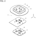
- FIGS. 2 and 3 show exploded perspective views of the connector 11.
- the connector 11 includes a top insulator 16 and a bottom insulator 17, and these top and bottom insulators 16 and 17 constitute the housing 12.
- the four plug contacts 13 are retained in the top insulator 16.
- the reinforcement sheet 14 is disposed on the bottom surface of the top insulator 16 on the -Z direction side, and the sheet type conductive member 15 is disposed on the -Z direction side of the reinforcement sheet 14.
- the bottom insulator 17 is disposed on the -Z direction side of the sheet type conductive member 15.
- the bottom insulator 17 is provided with four inner contacts 18. The four inner contacts 18 separately correspond to the four plug contacts 13.
- the top insulator 16 includes a recessed portion 16A opening in the +Z direction and four contact through-holes 16B formed within the recessed portion 16A.
- the recessed portion 16A constitutes a counter connector accommodating portion in which a part of a counter connector (not shown) is to be accommodated, and the four contact through-holes 16B correspond to the four plug contacts 13.
- a plurality of bosses 16C are formed to project in the -Z direction.
- the bottom insulator 17 includes a flat plate portion 17A, and the flat plate portion 17A is provided with four circular recessed portions 17B opening in the +Z direction.
- the four recessed portions 17B correspond to the four plug contacts 13.
- the four recessed portions 17B are each provided with an inner contact 18.
- the flat plate portion 17A is provided with a plurality of through-holes 17C corresponding to the bosses 16C of the top insulator 16.
- the inner contact 18 is formed from a projection 18A whose outer peripheral surface is entirely covered with a conductive layer, the projection 18A being made of the insulating material constituting the bottom insulator 17. That is, the projection 18A projects from the recessed portion 17B in the +Z direction along a fitting axis C, and the lateral surface of the projection 18A surrounding the fitting axis C and the top surface thereof facing the +Z direction are entirely covered with a continuous conductive layer.
- the conductive layer can be formed by subjecting the outer peripheral surface of the projection 18A of the bottom insulator 17 made of the insulating material to, for instance, electroless plating.
- the lateral surface of the projection 18A is provided with: two first protrusion portions 18B disposed on the opposite sides in the X direction across the fitting axis C; and four second protrusion portions 18C disposed at 90-degree intervals about the fitting axis C and each spaced from an adjacent first protrusion portion 18B at a 45-degree interval about the fitting axis C.
- the two first protrusion portions 18B protrude separately in the +X direction and in the -X direction.
- the four second protrusion portions 18C protrude separately in a direction inclined 45 degrees from the +X direction toward the +Y direction, a direction inclined 45 degrees from the +X direction toward the -Y direction, a direction inclined 45 degrees from the -X direction toward the +Y direction, and a direction inclined 45 degrees from the -X direction toward the -Y direction.
- the two first protrusion portions 18B are disposed at the same distance from the fitting axis C, and likewise, the four second protrusion portions 18C are disposed at the same distance from the fitting axis C.
- a first distance R1 from the fitting axis C to the tip of each first protrusion portion 18B is set larger than a second distance R2 from the fitting axis C to the tip of each second protrusion portion 18C.
- the tips of the two first protrusion portions 18B and the tips of the four second protrusion portions 18C are covered with the conductive layer covering the outer peripheral surface of the projection 18A.
- the conductive layer covering the tips of the two first protrusion portions 18B forms two contacting portions P1
- the conductive layer covering the tips of the four second protrusion portions 18C forms four pressing portions P2.
- the four plug contacts 13 are made of a conductive material such as metal, and are to be connected to corresponding contacts of a counter connector (not shown) when a part of the counter connector is accommodated in the recessed portion 16A of the top insulator 16.
- the plug contact 13 has a tubular portion 13A in the shape of a cylindrical tube extending in the Z direction along the fitting axis C and a flange 13B extending along an XY plane from the -Z directional end of the tubular portion 13A.
- the tubular portion 13A is provided in its interior with a recessed portion 13C opening toward the -Z direction.
- the fitting axis C is an axis passing through the center of the tubular portion 13A and extending in the direction in which the connector 11 and a counter connector are fitted to each other.
- tubular portion 13A has the shape of a cylindrical tube, the cross section thereof is not limited to a circle and may be any of various shapes such as an ellipse and a polygon as long as the tubular portion 13A has the recessed portion 13C in its interior.
- the four plug contacts 13 can be each used as a terminal for transmitting electric signals.
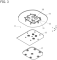
- the sheet type conductive member 15 has a multilayer structure in which a plurality of wiring layers each formed of a flexible conductor and a plurality of insulating layers are laminated.
- four contact arrangement regions 15A used to arrange the four plug contacts 13 are defined on the top surface, facing the +Z direction, of the sheet type conductive member 15.
- a wiring layer 15B is exposed toward the +Z direction in each of the four contact arrangement regions 15A, while an insulating layer 15C is exposed in a region other than the four contact arrangement regions 15A.
- the sheet type conductive member 15 is provided with four cross-shaped cuts 15D formed separately in the four contact arrangement regions 15A and penetrating the sheet type conductive member 15 in the Z direction.
- Each cut 15D is arranged such that the lines of the cross extend in the X direction and the Y direction. Since the cuts 15D penetrate the sheet type conductive member 15 in the Z direction, the cuts 15D are seen also on the bottom surface, facing the -Z direction, of the sheet type conductive member 15 in the positions corresponding to the four contact arrangement regions 15A as shown in FIG. 11 .
- a wiring layer 15E is exposed toward the -Z direction in the positions corresponding to the four contact arrangement regions 15A, while an insulating layer 15F is exposed in a region other than the regions corresponding to the four contact arrangement regions 15A.
- the sheet type conductive member 15 is provided at its peripheral portion with a plurality of through-holes 15G corresponding to the bosses 16C of the top insulator 16 as shown in FIGS. 10 and 11 .
- the first distance R1 from the fitting axis C of the inner contact 18 to the tip of each first protrusion portion 18B as shown in FIG. 7 is set slightly larger than the radius of the recessed portion 13C of the plug contact 13
- the second distance R2 from the fitting axis C of the inner contact 18 to the tip of each second protrusion portion 18C is set slightly larger than the value obtained by subtracting the thickness of the sheet type conductive member 15 from the radius of the recessed portion 13C of the plug contact 13.
- the reinforcement sheet 14 is provided to reinforce a mounting object (not shown) such as a garment on which the connector 11 is to be mounted.
- the reinforcement sheet 14 is made of an insulating material and provided at its center with an opening 14A. Further, a plurality of notches 14B corresponding to the bosses 16C of the top insulator 16 are formed along the periphery of the opening 14A of the reinforcement sheet 14.
- the four contact through-holes 16B of the top insulator 16, the four plug contacts 13, the four contact arrangement regions 15A of the sheet type conductive member 15, and the four inner contacts 18 of the bottom insulator 17 are arranged to align with one another in the Z direction.
- the bosses 16C of the top insulator 16, the notches 14B of the reinforcement sheet 14, the through-holes 15G of the sheet type conductive member 15, and the through-holes 17C of the bottom insulator 17 are arranged to align with one another in the Z direction.
- the bosses 16C of the top insulator 16 are inserted into the notches 14B of the reinforcement sheet 14. At this time, the four contact through-holes 16B of the top insulator 16 are situated inside the opening 14A of the reinforcement sheet 14.
- tubular portions 13A of the plug contacts 13 are inserted into the four contact through-holes 16B of the top insulator 16 correspondingly from the -Z direction, and the bottom insulator 17 is pressed against the top insulator 16 in the +Z direction with the sheet type conductive member 15 being sandwiched therebetween.
- each plug contact 13 is situated above the corresponding contact arrangement region 15A of the sheet type conductive member 15, and each inner contact 18 formed on the bottom insulator 17 is inserted into the recessed portion 13C of the corresponding plug contact 13 while pushing the corresponding contact arrangement region 15A of the sheet type conductive member 15.
- the four inner contacts 18 are each inserted into the recessed portion 13C of the corresponding plug contact 13 while opening the cut 15D of the corresponding contact arrangement region 15A.
- the bosses 16C of the top insulator 16 sequentially pass through the notches 14B of the reinforcement sheet 14, the through-holes 15G of the sheet type conductive member 15, and the through-holes 17C of the bottom insulator 17. Then, the ends of the bosses 16C projecting on the -Z directional side of the bottom insulator 17 are heated and deformed as shown in FIG. 13 , whereby the top insulator 16 and the bottom insulator 17 are fixed to each other. Thus, the assembling operation of the connector 11 is completed.
- plug contacts 13 are fixed to the top insulator 16 and the bottom insulator 17 because their flanges 13B are sandwiched between the top insulator 16 and the bottom insulator 17.
- the four second protrusion portions 18C of the inner contact 18 each protrude in a direction inclined 45 degrees with respect to the X direction and the Y direction in an XY plane as shown in FIG. 7 , and the four cuts 15D of the sheet type conductive member 15 are each arranged such that the lines of the cross extend in the X direction and the Y direction as shown in FIGS. 10 and 11 .
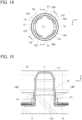
- the two first protrusion portions 18B of the inner contact 18 are to be situated inside the opened cut 15D of the sheet type conductive member 15 when the inner contact 18 is inserted in the recessed portion 13C of the plug contact 13 because the first protrusion portions 18B protrude separately in the +X direction and the -X direction in an XY plane. Accordingly, the contacting portions P1 formed at the tips of the two first protrusion portions 18B of the inner contact 18 directly face the inner surface of the recessed portion 13C of the plug contact 13 as shown in FIG. 14 .
- the first distance R1 from the fitting axis C of the inner contact 18 to the tip of each first protrusion portion 18B is set slightly larger than the radius of the recessed portion 13C of the plug contact 13, when the inner contact 18 is inserted in the recessed portion 13C of the plug contact 13, pushing forces of the tip of the first protrusion portion 18B of the inner contact 18 and the inner surface of the recessed portion 13C of the plug contact 13 act on each other. Consequently, at least one of the first protrusion portion 18B or the plug contact 13 deforms, and as shown in FIG.
- the pair of contacting portions P1 formed at the tips of the two first protrusion portions 18B of the inner contact 18 are pressed against the inner surface of the recessed portion 13C of the plug contact 13, whereby the inner contact 18 is electrically connected to the plug contact 13.
- the second distance R2 from the fitting axis C of the inner contact 18 to the tip of each second protrusion portion 18C is set slightly larger than the value obtained by subtracting the thickness of the sheet type conductive member 15 from the radius of the recessed portion 13C of the plug contact 13, when the inner contact 18 is inserted in the recessed portion 13C of the plug contact 13, pushing forces of the tip of the second protrusion portion 18C of the inner contact 18 and the inner surface of the recessed portion 13C of the plug contact 13 act on each other. Consequently, at least one of the second protrusion portion 18C, the sheet type conductive member 15, or the plug contact 13 deforms, and as shown in FIG.
- the sheet type conductive member 15 sandwiched between the pressing portions P2 formed at the tips of the second protrusion portions 18C of the inner contact 18 and the inner surface of the recessed portion 13C of the plug contact 13 is pressed against the inner surface of the recessed portion 13C of the plug contact 13 by the pressing portions P2.
- the sheet type conductive member 15 is pressed against the inner surface of the recessed portion 13C of the plug contact 13 by the four pressing portions P2 formed at the tips of the four second protrusion portions 18C of the inner contact 18.
- the wiring layer 15B is exposed in the contact arrangement regions 15A on the top surface of the sheet type conductive member 15, and the wiring layer 15E is exposed in the positions corresponding to the contact arrangement regions 15A on the bottom surface of the sheet type conductive member 15.
- the wiring layer 15B on the top surface of the sheet type conductive member 15 makes contact with the inner surface of the recessed portion 13C of the plug contact 13 at a predetermined contact pressure, while the wiring layer 15E on the bottom surface of the sheet type conductive member 15 makes contact with the pressing portions P2 of the inner contact 18 at a predetermined contact pressure.
- the wiring layer 15B exposed on the top surface of the sheet type conductive member 15 is electrically connected to the plug contact 13 directly, and the wiring layer 15E exposed on the bottom surface of the sheet type conductive member 15 is electrically connected to the plug contact 13 via the inner contact 18. In other words, both the wiring layers 15B and 15E are connected the plug contact 13.
- both the wiring layer 15B formed of a flexible conductor disposed on the top surface side of the sheet type conductive member 15 and the wiring layer 15E formed of a flexible conductor disposed on the bottom surface side of the same can be electrically connected to one plug contact 13 by use of the inner contact 18.
- the plug contact 13 can be electrically connected to the flexible conductor on the top surface side of the sheet type conductive member, and when the connector 11 is connected to a sheet type conductive member having a flexible conductor exposed only on the bottom surface side, the plug contact 13 can be electrically connected to the flexible conductor on the bottom surface side of the sheet type conductive member.
- the plug contact 13 can be electrically connected to both the flexible conductor on the top surface side and the flexible conductor on the bottom surface side of the sheet type conductive member.
- the reinforcement sheet 14 is disposed between the bottom insulator 17 and the top insulator 16 in the connector 11 of Embodiment 1, the reinforcement sheet 14 may be omitted when it is not necessary to reinforce the mounting object such as a garment on which the connector 11 is to be mounted.
- the inner contact 18 used in the connector 11 of Embodiment 1 has the two first protrusion portions 18B and the four second protrusion portions 18C, the invention is not limited thereto.
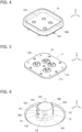
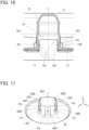
- FIGS. 17 and 18 show an inner contact 28 used in a connector according to Embodiment 2.
- This inner contact 28 includes four first protrusion portions 28B and four second protrusion portions 28C that are arranged on the lateral side of a projection 28A projecting in the +Z direction along the fitting axis C.
- the four first protrusion portions 28B are arranged at 90-degree intervals about the fitting axis C in an XY plane.
- the four second protrusion portions 28C are also arranged at 90-degree intervals about the fitting axis C in an XY plane but are situated in rotational positions that are 45 degrees off from the four first protrusion portions 28B about the fitting axis C. That is, each second protrusion portion 28C is spaced from an adjacent first protrusion portion 28B at a 45-degree interval about the fitting axis C.
- an outer peripheral surface of the projection 28A is entirely covered with a conductive layer, the conductive layer covering the tips of the four first protrusion portions 28B forms four contacting portions P1, and the conductive layer covering the tips of the four second protrusion portions 28C forms four pressing portions P2.
- a distance from the fitting axis C to the tip of each first protrusion portion 28B and a distance from the fitting axis C to the tip of each second protrusion portion 28C are the same as the first distance R1 from the fitting axis C to the tip of each first protrusion portion 18B and the second distance R2 from the fitting axis C to the tip of each second protrusion portion 18C in the inner contact 18 shown in FIG. 7 , respectively.
- the four contacting portions P1 are pressed against the inner surface of the recessed portion 13C of the plug contact 13 so that the inner contact 28 is electrically connected to the plug contact 13, and the sheet type conductive member 15 pushed in the recessed portion 13C is pressed against the inner surface of the recessed portion 13C of the plug contact 13 by the four pressing portions P2 of the inner contact 28.
- both the wiring layer 15B disposed on the top surface side of the sheet type conductive member 15 and the wiring layer 15E disposed on the bottom surface side of the same can be electrically connected to the plug contact 13 even when the inner contact 18 is replaced by the inner contact 28 shown in FIGS. 17 and 18 in the connector 11 according to Embodiment 1.
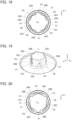
- FIGS. 19 and 20 show an inner contact 38 used in a connector according to Embodiment 3.
- This inner contact 38 includes three first protrusion portions 38B and three second protrusion portions 38C that are arranged on the lateral side of a projection 38A projecting in the +Z direction along the fitting axis C.
- the three first protrusion portions 38B are arranged at 120-degree intervals about the fitting axis C in an XY plane.
- the three second protrusion portions 38C are also arranged at 120-degree intervals about the fitting axis C in an XY plane but are situated in rotational positions that are 60 degrees off from the three first protrusion portions 38B about the fitting axis C. That is, each second protrusion portion 38C is spaced from an adjacent first protrusion portion 38B at a 60-degree interval about the fitting axis C.
- an outer peripheral surface of the projection 38A is entirely covered with a conductive layer, the conductive layer covering the tips of the three first protrusion portions 38B forms three contacting portions P1, and the conductive layer covering the tips of the three second protrusion portions 38C forms three pressing portions P2.
- a distance from the fitting axis C to the tip of each first protrusion portion 38B and a distance from the fitting axis C to the tip of each second protrusion portion 38C are the same as the first distance R1 from the fitting axis C to the tip of each first protrusion portion 18B and the second distance R2 from the fitting axis C to the tip of each second protrusion portion 18C in the inner contact 18 shown in FIG. 7 , respectively.
- the sheet type conductive member 15 shown in FIGS. 10 and 11 has a cross-shaped cut 15D in each contact arrangement region 15A, for the inner contact 38 in Embodiment 3, it is preferable to use a sheet type conductive member with a Y-shaped cut having three cut lines extending from the center of the contact arrangement region 15A at 120-degree intervals, instead of the cross-shaped cut 15D. Furthermore, preferably, the orientations of the inner contact 38 and the corresponding Y-shaped cut are adjusted such that the three first protrusion portions 38B of the inner contact 38 overlap the three cut lines of the Y-shaped cut.
- the inner contact 38 is electrically connected to the plug contact 13, and the sheet type conductive member 15 pushed in the recessed portion 13C is pressed against the inner surface of the recessed portion 13C of the plug contact 13 by the three pressing portions P2 of the inner contact 38.
- both the wiring layer 15B disposed on the top surface side of the sheet type conductive member 15 and the wiring layer 15E disposed on the bottom surface side of the same can be electrically connected to the plug contact 13 even when the inner contact 18 is replaced by the inner contact 38 shown in FIGS. 19 and 20 in the connector 11 according to Embodiment 1.
- the plug contacts 13 disposed in the contact arrangement regions 15A of the sheet type conductive member 15 each make contact with both the wiring layer 15B exposed on the top surface side of the sheet type conductive member 15 and the wiring layer 15E exposed on the bottom surface side of the sheet type conductive member 15; however, for instance, it is also possible to connect only the wiring layer 15E exposed on the bottom surface side of the sheet type conductive member 15 to the plug contacts 13 disposed in the contact arrangement regions 15A.
- the sheet type conductive member 15 used in Embodiments 1 to 3 above has a multilayer structure, the invention is not limited thereto, and it is sufficient that a conductive member has a flexible conductor exposed on at least one surface of the conductive member.
- the invention is not limited thereto, and three or more layers of flexible conductors can be connected to one plug contact 13.
- the connector 11 according to Embodiments 1 to 3 above has four plug contacts 13, the number of the plug contacts 13 is not limited, and it is sufficient that there is provided at least one plug contact 13 electrically connected to a flexible conductor exposed on at least one surface of the sheet type conductive member 15.
Landscapes
- Coupling Device And Connection With Printed Circuit (AREA)
Claims (10)
- Verbinder, aufweisend:einen Steckkontakt (13), der eine leitende Eigenschaft besitzt, eine Röhrenform aufweist und einen ausgesparten Abschnitt (13C) aufweist, der sich entlang einer Montageachse (C) erstreckt; undeinen inneren Kontakt (18, 28, 38), der aus einem Vorsprung (18A, 28A, 38A) besteht, der in den ausgesparten Abschnitt eingeführt ist und eine Außenumfangsfläche aufweist, die vollständig mit einer leitfähigen Schicht überzogen ist,wobei der innere Kontakt einen Kontaktierungsabschnitt (P1), der Kontakt mit dem Steckkontakt innerhalb des ausgesparten Abschnitts herstellt, und einen Drückabschnitt (P2), der sich in einer von dem Kontaktierungsabschnitt verschiedenen Drehposition um die Montageachse befindet, aufweist undein Teil eines Verbindungsobjekts (15) vom Flachmaterialtyp, der einen flexiblen Leiter (15B, 15E) aufweist, der an mindestens einer Fläche des Verbindungsobjekts frei liegt, zwischen dem Drückabschnitt und einer Innenfläche des ausgesparten Abschnitts in einer Richtung senkrecht zu der Montageachse sandwichartig angeordnet ist, die Innenfläche des ausgesparten Abschnitts Kontakt mit einer Oberseite des Verbindungsobjekts herstellt und der Drückabschnitt Kontakt mit einer Unterseite des Verbindungsobjekts herstellt, wodurch der Steckkontakt direkt elektrisch mit dem flexiblen Leiter verbunden ist, wenn der flexible Leiter an der Oberseite des Verbindungsobjekts frei liegt, und der Steckkontakt über den inneren Kontakt elektrisch mit dem flexiblen Leiter verbunden ist, wenn der flexible Leiter an der Unterseite des Verbindungsobjekts frei liegt.
- Verbinder nach Anspruch 1,
wobei der Vorsprung (18A, 28A, 38A) aufweist:mindestens einen ersten Vorsprungsabschnitt (18B, 28B, 38B), der in einer Richtung senkrecht zu der Montageachse vorsteht; undmindestens einen zweiten Vorsprungsabschnitt (18C, 28C, 38C), der in einer Richtung senkrecht zu der Montageachse in einer von dem mindestens einen ersten Vorsprungsabschnitt verschiedenen Drehposition um die Montageachse vorsteht,die leitfähige Schicht, die eine Spitze jedes des mindestens einen ersten Vorsprungsabschnitts bedeckt, den Kontaktierungsabschnitt (P1) bildet, unddie leitfähige Schicht, die eine Spitze jedes des mindestens einen zweiten Vorsprungsabschnitts bedeckt, den Drückabschnitt (P2) bildet. - Verbinder nach Anspruch 2,
wobei eine erste Distanz (R1) von der Montageachse zu dem Kontaktierungsabschnitt größer ist als eine zweite Distanz (R2) von der Montageachse zu dem Drückabschnitt in einer Richtung senkrecht zu der Montageachse. - Verbinder nach Anspruch 3,wobei die erste Distanz (R1) geringfügig größer ist als ein Radius des ausgesparten Abschnitts (13C), unddie zweite Distanz (R2) geringfügig größer ist als ein Wert, der durch Subtrahieren einer Dicke des Verbindungsobjekts von dem Radius des ausgesparten Abschnitts erhalten wird.
- Verbinder nach einem der Ansprüche 2-4,
wobei der Vorsprung (18A, 28A, 38A) mehrere der ersten Vorsprungsabschnitte (18B, 28B, 38B) und mehrere der zweiten Vorsprungsabschnitte (18C, 28C, 38C) aufweist. - Verbinder nach Anspruch 5,
wobei der Vorsprung (18A) aufweist:zwei erste Vorsprungsabschnitte (18B), die an entgegengesetzten Seiten quer zu der Montageachse als die mehreren der ersten Vorsprungsabschnitte angeordnet sind; undvier zweite Vorsprungsabschnitte (18C), die in 90-Grad-Intervallen um die Montageachse angeordnet sind und jeweils von einem benachbarten der zwei ersten Vorsprungsabschnitte in einem 45-Grad-Intervall um die Montageachse als die mehreren der zweiten Vorsprungsabschnitte beabstandet sind. - Verbinder nach Anspruch 5,
wobei der Vorsprung (28A) aufweist:vier erste Vorsprungsabschnitte (28B), die in 90-Grad-Intervallen um die Montageachse als die mehreren der ersten Vorsprungsabschnitte angeordnet sind; undvier zweite Vorsprungsabschnitte (28C), die in 90-Grad-Intervallen um die Montageachse angeordnet sind und jeweils von einem benachbarten der vier ersten Vorsprungsabschnitte in einem 45-Grad-Intervall um die Montageachse als die mehreren der zweiten Vorsprungsabschnitte beabstandet sind. - Verbinder nach Anspruch 5,
wobei der Vorsprung (38A) aufweist:drei erste Vorsprungsabschnitte (38B), die in 120-Grad-Intervallen um die Montageachse als die mehreren der ersten Vorsprungsabschnitte angeordnet sind; unddrei zweite Vorsprungsabschnitte (38C), die in 120-Grad-Intervallen um die Montageachse angeordnet sind und jeweils von einem benachbarten der drei ersten Vorsprungsabschnitte in einem 60-Grad-Intervall um die Montageachse als die mehreren der zweiten Vorsprungsabschnitte beabstandet sind. - Verbinder nach Anspruch 1,
wobei der Steckkontakt (13) einen röhrenförmigen Abschnitt (13A) und einen Flansch (13B), der an einem Ende des röhrenförmigen Abschnitts ausgebildet ist, aufweist und der ausgesparte Abschnitt (13C) aus einem Inneren des röhrenförmigen Abschnitts gebildet ist. - Verbinder nach Anspruch 9, der ein Gehäuse (12) aufweist, das eine isolierende Eigenschaft besitzt und dazu eingerichtet ist, das Verbindungsobjekt (15) und den Steckkontakt (13) zu halten,
wobei das Gehäuse aufweist:einen oberen Isolator (16), der mit einem Kontaktdurchgangsloch (16B) versehen ist, durch das hindurch der röhrenförmige Abschnitt des Steckkontakts führt und das kleiner als der Flansch ist; undeinen unteren Isolator (17), der mit dem inneren Kontakt (128, 28, 38) versehen ist, undder obere Isolator so an dem unteren Isolator befestigt ist, dass der röhrenförmige Abschnitt des Steckkontakts durch das Kontaktdurchgangsloch hindurch führt und das Verbindungsobjekt und der Flansch zwischen dem oberen Isolator und dem unteren Isolator sandwichartig angeordnet sind.
Applications Claiming Priority (1)
| Application Number | Priority Date | Filing Date | Title |
|---|---|---|---|
| JP2022139302A JP2024034807A (ja) | 2022-09-01 | 2022-09-01 | コネクタ |
Publications (2)
| Publication Number | Publication Date |
|---|---|
| EP4333216A1 EP4333216A1 (de) | 2024-03-06 |
| EP4333216B1 true EP4333216B1 (de) | 2025-01-22 |
Family
ID=87419146
Family Applications (1)
| Application Number | Title | Priority Date | Filing Date |
|---|---|---|---|
| EP23186205.3A Active EP4333216B1 (de) | 2022-09-01 | 2023-07-18 | Verbinder |
Country Status (4)
| Country | Link |
|---|---|
| US (1) | US20240079809A1 (de) |
| EP (1) | EP4333216B1 (de) |
| JP (1) | JP2024034807A (de) |
| CN (1) | CN117638532A (de) |
Family Cites Families (7)
| Publication number | Priority date | Publication date | Assignee | Title |
|---|---|---|---|---|
| JP6840559B2 (ja) | 2017-02-10 | 2021-03-10 | 日本航空電子工業株式会社 | コネクタ |
| JP7232143B2 (ja) * | 2019-07-19 | 2023-03-02 | 日本航空電子工業株式会社 | コネクタ |
| JP7348016B2 (ja) * | 2019-10-01 | 2023-09-20 | 日本航空電子工業株式会社 | コネクタ |
| JP7348060B2 (ja) * | 2019-10-03 | 2023-09-20 | 日本航空電子工業株式会社 | コネクタおよび接続方法 |
| US11258189B2 (en) * | 2019-10-03 | 2022-02-22 | Japan Aviation Electronics Industry, Limited | Connector and connecting method |
| JP2024030814A (ja) * | 2022-08-25 | 2024-03-07 | 日本航空電子工業株式会社 | コネクタ |
| JP2024094608A (ja) * | 2022-12-28 | 2024-07-10 | 日本航空電子工業株式会社 | コネクタおよび接続方法 |
-
2022
- 2022-09-01 JP JP2022139302A patent/JP2024034807A/ja active Pending
-
2023
- 2023-07-17 US US18/222,654 patent/US20240079809A1/en active Pending
- 2023-07-18 EP EP23186205.3A patent/EP4333216B1/de active Active
- 2023-07-20 CN CN202310899304.5A patent/CN117638532A/zh active Pending
Also Published As
| Publication number | Publication date |
|---|---|
| EP4333216A1 (de) | 2024-03-06 |
| JP2024034807A (ja) | 2024-03-13 |
| CN117638532A (zh) | 2024-03-01 |
| US20240079809A1 (en) | 2024-03-07 |
Similar Documents
| Publication | Publication Date | Title |
|---|---|---|
| EP4346017B1 (de) | Verbinder | |
| US12424774B2 (en) | Connector | |
| EP4329104B1 (de) | Verbinder | |
| EP4300713B1 (de) | Blattartiges leitfähiges element und verbinder | |
| EP4395079B1 (de) | Verbinder und verbindungsverfahren | |
| EP4333216B1 (de) | Verbinder | |
| US20240380148A1 (en) | Connector | |
| US12567691B2 (en) | Connector | |
| JP2024021591A (ja) | コネクタ | |
| EP4507128B1 (de) | Verbinder und verbinderanordnung | |
| CN117638542A (zh) | 连接器和连接器组装体 | |
| EP4611180A1 (de) | Verbinder | |
| US12537336B2 (en) | Connector |
Legal Events
| Date | Code | Title | Description |
|---|---|---|---|
| PUAI | Public reference made under article 153(3) epc to a published international application that has entered the european phase |
Free format text: ORIGINAL CODE: 0009012 |
|
| STAA | Information on the status of an ep patent application or granted ep patent |
Free format text: STATUS: REQUEST FOR EXAMINATION WAS MADE |
|
| 17P | Request for examination filed |
Effective date: 20230718 |
|
| AK | Designated contracting states |
Kind code of ref document: A1 Designated state(s): AL AT BE BG CH CY CZ DE DK EE ES FI FR GB GR HR HU IE IS IT LI LT LU LV MC ME MK MT NL NO PL PT RO RS SE SI SK SM TR |
|
| RBV | Designated contracting states (corrected) |
Designated state(s): AL AT BE BG CH CY CZ DE DK EE ES FI FR GB GR HR HU IE IS IT LI LT LU LV MC ME MK MT NL NO PL PT RO RS SE SI SK SM TR |
|
| GRAP | Despatch of communication of intention to grant a patent |
Free format text: ORIGINAL CODE: EPIDOSNIGR1 |
|
| STAA | Information on the status of an ep patent application or granted ep patent |
Free format text: STATUS: GRANT OF PATENT IS INTENDED |
|
| INTG | Intention to grant announced |
Effective date: 20240916 |
|
| RAP3 | Party data changed (applicant data changed or rights of an application transferred) |
Owner name: JAPAN AVIATION ELECTRONICS INDUSTRY, LTD. |
|
| GRAS | Grant fee paid |
Free format text: ORIGINAL CODE: EPIDOSNIGR3 |
|
| GRAA | (expected) grant |
Free format text: ORIGINAL CODE: 0009210 |
|
| STAA | Information on the status of an ep patent application or granted ep patent |
Free format text: STATUS: THE PATENT HAS BEEN GRANTED |
|
| AK | Designated contracting states |
Kind code of ref document: B1 Designated state(s): AL AT BE BG CH CY CZ DE DK EE ES FI FR GB GR HR HU IE IS IT LI LT LU LV MC ME MK MT NL NO PL PT RO RS SE SI SK SM TR |
|
| REG | Reference to a national code |
Ref country code: GB Ref legal event code: FG4D |
|
| REG | Reference to a national code |
Ref country code: CH Ref legal event code: EP |
|
| REG | Reference to a national code |
Ref country code: IE Ref legal event code: FG4D |
|
| REG | Reference to a national code |
Ref country code: DE Ref legal event code: R096 Ref document number: 602023001754 Country of ref document: DE |
|
| REG | Reference to a national code |
Ref country code: NL Ref legal event code: MP Effective date: 20250122 |
|
| PG25 | Lapsed in a contracting state [announced via postgrant information from national office to epo] |
Ref country code: NL Free format text: LAPSE BECAUSE OF FAILURE TO SUBMIT A TRANSLATION OF THE DESCRIPTION OR TO PAY THE FEE WITHIN THE PRESCRIBED TIME-LIMIT Effective date: 20250122 |
|
| PG25 | Lapsed in a contracting state [announced via postgrant information from national office to epo] |
Ref country code: RS Free format text: LAPSE BECAUSE OF FAILURE TO SUBMIT A TRANSLATION OF THE DESCRIPTION OR TO PAY THE FEE WITHIN THE PRESCRIBED TIME-LIMIT Effective date: 20250422 |
|
| PG25 | Lapsed in a contracting state [announced via postgrant information from national office to epo] |
Ref country code: FI Free format text: LAPSE BECAUSE OF FAILURE TO SUBMIT A TRANSLATION OF THE DESCRIPTION OR TO PAY THE FEE WITHIN THE PRESCRIBED TIME-LIMIT Effective date: 20250122 |
|
| PG25 | Lapsed in a contracting state [announced via postgrant information from national office to epo] |
Ref country code: PL Free format text: LAPSE BECAUSE OF FAILURE TO SUBMIT A TRANSLATION OF THE DESCRIPTION OR TO PAY THE FEE WITHIN THE PRESCRIBED TIME-LIMIT Effective date: 20250122 |
|
| PG25 | Lapsed in a contracting state [announced via postgrant information from national office to epo] |
Ref country code: ES Free format text: LAPSE BECAUSE OF FAILURE TO SUBMIT A TRANSLATION OF THE DESCRIPTION OR TO PAY THE FEE WITHIN THE PRESCRIBED TIME-LIMIT Effective date: 20250122 |
|
| REG | Reference to a national code |
Ref country code: LT Ref legal event code: MG9D |
|
| PG25 | Lapsed in a contracting state [announced via postgrant information from national office to epo] |
Ref country code: NO Free format text: LAPSE BECAUSE OF FAILURE TO SUBMIT A TRANSLATION OF THE DESCRIPTION OR TO PAY THE FEE WITHIN THE PRESCRIBED TIME-LIMIT Effective date: 20250422 Ref country code: IS Free format text: LAPSE BECAUSE OF FAILURE TO SUBMIT A TRANSLATION OF THE DESCRIPTION OR TO PAY THE FEE WITHIN THE PRESCRIBED TIME-LIMIT Effective date: 20250522 |
|
| REG | Reference to a national code |
Ref country code: AT Ref legal event code: MK05 Ref document number: 1762183 Country of ref document: AT Kind code of ref document: T Effective date: 20250122 |
|
| PG25 | Lapsed in a contracting state [announced via postgrant information from national office to epo] |
Ref country code: HR Free format text: LAPSE BECAUSE OF FAILURE TO SUBMIT A TRANSLATION OF THE DESCRIPTION OR TO PAY THE FEE WITHIN THE PRESCRIBED TIME-LIMIT Effective date: 20250122 |
|
| PG25 | Lapsed in a contracting state [announced via postgrant information from national office to epo] |
Ref country code: LV Free format text: LAPSE BECAUSE OF FAILURE TO SUBMIT A TRANSLATION OF THE DESCRIPTION OR TO PAY THE FEE WITHIN THE PRESCRIBED TIME-LIMIT Effective date: 20250122 Ref country code: PT Free format text: LAPSE BECAUSE OF FAILURE TO SUBMIT A TRANSLATION OF THE DESCRIPTION OR TO PAY THE FEE WITHIN THE PRESCRIBED TIME-LIMIT Effective date: 20250522 |
|
| PG25 | Lapsed in a contracting state [announced via postgrant information from national office to epo] |
Ref country code: BG Free format text: LAPSE BECAUSE OF FAILURE TO SUBMIT A TRANSLATION OF THE DESCRIPTION OR TO PAY THE FEE WITHIN THE PRESCRIBED TIME-LIMIT Effective date: 20250122 Ref country code: GR Free format text: LAPSE BECAUSE OF FAILURE TO SUBMIT A TRANSLATION OF THE DESCRIPTION OR TO PAY THE FEE WITHIN THE PRESCRIBED TIME-LIMIT Effective date: 20250423 |
|
| PG25 | Lapsed in a contracting state [announced via postgrant information from national office to epo] |
Ref country code: AT Free format text: LAPSE BECAUSE OF FAILURE TO SUBMIT A TRANSLATION OF THE DESCRIPTION OR TO PAY THE FEE WITHIN THE PRESCRIBED TIME-LIMIT Effective date: 20250122 |
|
| PG25 | Lapsed in a contracting state [announced via postgrant information from national office to epo] |
Ref country code: SE Free format text: LAPSE BECAUSE OF FAILURE TO SUBMIT A TRANSLATION OF THE DESCRIPTION OR TO PAY THE FEE WITHIN THE PRESCRIBED TIME-LIMIT Effective date: 20250122 |
|
| PG25 | Lapsed in a contracting state [announced via postgrant information from national office to epo] |
Ref country code: SM Free format text: LAPSE BECAUSE OF FAILURE TO SUBMIT A TRANSLATION OF THE DESCRIPTION OR TO PAY THE FEE WITHIN THE PRESCRIBED TIME-LIMIT Effective date: 20250122 |
|
| PG25 | Lapsed in a contracting state [announced via postgrant information from national office to epo] |
Ref country code: DK Free format text: LAPSE BECAUSE OF FAILURE TO SUBMIT A TRANSLATION OF THE DESCRIPTION OR TO PAY THE FEE WITHIN THE PRESCRIBED TIME-LIMIT Effective date: 20250122 |
|
| PGFP | Annual fee paid to national office [announced via postgrant information from national office to epo] |
Ref country code: DE Payment date: 20250708 Year of fee payment: 3 |
|
| PG25 | Lapsed in a contracting state [announced via postgrant information from national office to epo] |
Ref country code: IT Free format text: LAPSE BECAUSE OF FAILURE TO SUBMIT A TRANSLATION OF THE DESCRIPTION OR TO PAY THE FEE WITHIN THE PRESCRIBED TIME-LIMIT Effective date: 20250122 |
|
| PGFP | Annual fee paid to national office [announced via postgrant information from national office to epo] |
Ref country code: FR Payment date: 20250725 Year of fee payment: 3 |
|
| PG25 | Lapsed in a contracting state [announced via postgrant information from national office to epo] |
Ref country code: EE Free format text: LAPSE BECAUSE OF FAILURE TO SUBMIT A TRANSLATION OF THE DESCRIPTION OR TO PAY THE FEE WITHIN THE PRESCRIBED TIME-LIMIT Effective date: 20250122 Ref country code: CZ Free format text: LAPSE BECAUSE OF FAILURE TO SUBMIT A TRANSLATION OF THE DESCRIPTION OR TO PAY THE FEE WITHIN THE PRESCRIBED TIME-LIMIT Effective date: 20250122 |
|
| REG | Reference to a national code |
Ref country code: DE Ref legal event code: R097 Ref document number: 602023001754 Country of ref document: DE |
|
| PG25 | Lapsed in a contracting state [announced via postgrant information from national office to epo] |
Ref country code: RO Free format text: LAPSE BECAUSE OF FAILURE TO SUBMIT A TRANSLATION OF THE DESCRIPTION OR TO PAY THE FEE WITHIN THE PRESCRIBED TIME-LIMIT Effective date: 20250122 |
|
| PG25 | Lapsed in a contracting state [announced via postgrant information from national office to epo] |
Ref country code: SK Free format text: LAPSE BECAUSE OF FAILURE TO SUBMIT A TRANSLATION OF THE DESCRIPTION OR TO PAY THE FEE WITHIN THE PRESCRIBED TIME-LIMIT Effective date: 20250122 |
|
| PLBE | No opposition filed within time limit |
Free format text: ORIGINAL CODE: 0009261 |
|
| STAA | Information on the status of an ep patent application or granted ep patent |
Free format text: STATUS: NO OPPOSITION FILED WITHIN TIME LIMIT |
|
| 26N | No opposition filed |
Effective date: 20251023 |
|
| PG25 | Lapsed in a contracting state [announced via postgrant information from national office to epo] |
Ref country code: LU Free format text: LAPSE BECAUSE OF NON-PAYMENT OF DUE FEES Effective date: 20250718 |