EP4064336A1 - Halbleiterbauelement - Google Patents
Halbleiterbauelement Download PDFInfo
- Publication number
- EP4064336A1 EP4064336A1 EP22173123.5A EP22173123A EP4064336A1 EP 4064336 A1 EP4064336 A1 EP 4064336A1 EP 22173123 A EP22173123 A EP 22173123A EP 4064336 A1 EP4064336 A1 EP 4064336A1
- Authority
- EP
- European Patent Office
- Prior art keywords
- wall
- cooling
- fins
- semiconductor device
- side wall
- Prior art date
- Legal status (The legal status is an assumption and is not a legal conclusion. Google has not performed a legal analysis and makes no representation as to the accuracy of the status listed.)
- Pending
Links
Images




Classifications
-
- H—ELECTRICITY
- H10—SEMICONDUCTOR DEVICES; ELECTRIC SOLID-STATE DEVICES NOT OTHERWISE PROVIDED FOR
- H10W—GENERIC PACKAGES, INTERCONNECTIONS, CONNECTORS OR OTHER CONSTRUCTIONAL DETAILS OF DEVICES COVERED BY CLASS H10
- H10W40/00—Arrangements for thermal protection or thermal control
- H10W40/20—Arrangements for cooling
- H10W40/22—Arrangements for cooling characterised by their shape, e.g. having conical or cylindrical projections
- H10W40/226—Arrangements for cooling characterised by their shape, e.g. having conical or cylindrical projections characterised by projecting parts, e.g. fins to increase surface area
-
- H—ELECTRICITY
- H05—ELECTRIC TECHNIQUES NOT OTHERWISE PROVIDED FOR
- H05K—PRINTED CIRCUITS; CASINGS OR CONSTRUCTIONAL DETAILS OF ELECTRIC APPARATUS; MANUFACTURE OF ASSEMBLAGES OF ELECTRICAL COMPONENTS
- H05K7/00—Constructional details common to different types of electric apparatus
- H05K7/20—Modifications to facilitate cooling, ventilating, or heating
- H05K7/2089—Modifications to facilitate cooling, ventilating, or heating for power electronics, e.g. for inverters for controlling motor
- H05K7/20927—Liquid coolant without phase change
-
- H—ELECTRICITY
- H10—SEMICONDUCTOR DEVICES; ELECTRIC SOLID-STATE DEVICES NOT OTHERWISE PROVIDED FOR
- H10W—GENERIC PACKAGES, INTERCONNECTIONS, CONNECTORS OR OTHER CONSTRUCTIONAL DETAILS OF DEVICES COVERED BY CLASS H10
- H10W40/00—Arrangements for thermal protection or thermal control
- H10W40/20—Arrangements for cooling
- H10W40/22—Arrangements for cooling characterised by their shape, e.g. having conical or cylindrical projections
-
- H—ELECTRICITY
- H10—SEMICONDUCTOR DEVICES; ELECTRIC SOLID-STATE DEVICES NOT OTHERWISE PROVIDED FOR
- H10W—GENERIC PACKAGES, INTERCONNECTIONS, CONNECTORS OR OTHER CONSTRUCTIONAL DETAILS OF DEVICES COVERED BY CLASS H10
- H10W40/00—Arrangements for thermal protection or thermal control
- H10W40/40—Arrangements for thermal protection or thermal control involving heat exchange by flowing fluids
- H10W40/47—Arrangements for thermal protection or thermal control involving heat exchange by flowing fluids by flowing liquids, e.g. forced water cooling
Definitions
- the present invention relates to a semiconductor device equipped with a cooling device for cooling semiconductor elements.
- Apparatuses using electric motors use power conversion devices to save energy.
- Such power conversion devices typically use a semiconductor module.
- the semiconductor module constituting a control device serving to save energy is provided with a power semiconductor element that controls a large electric current.
- the usual power semiconductor element generates heat when a large electric current is controlled, and the amount of the generated heat increases with the miniaturization and increase in output of the power conversion device. Therefore, in a case of a semiconductor module provided with a plurality of power semiconductor elements, cooling the semiconductor module is a significant problem.
- Cooling devices of a liquid cooling system have been used as cooling devices to be attached to semiconductor modules in order to cool the modules.
- a cooling device of a liquid cooling system is provided with a heat radiation substrate that is made from a metal and joined to an insulating substrate carrying the power semiconductor elements on the side thereof opposite that where the semiconductor module is disposed, heat radiation fins formed integrally with the heat radiation substrate, and a box-shaped cooling case that accommodates the fins and is liquid tightly attached to the heat radiation substrate.
- An introducing port and a discharge port for a cooling medium (cooling liquid) are connected to the cooling case.
- a flow path is formed inside the cooling case for the cooling medium introduced into the cooling case from the introducing port to pass through the fins and be discharged from the discharge port.
- the cooling medium for example, water or a long-life coolant
- the cooling medium pressurized by an external pump is introduced from the introducing port and flows through the flow path inside the cooling case.
- the cooling medium is discharged from the discharge port, cooled in an external heat exchanger, pressurized by the pump, and then returned into the flow path inside the cooling case.
- a cooling device of such type in which an inlet and an outlet for a cooling medium are provided at the longitudinal ends of the cooling device, fins provided correspondingly to a plurality of semiconductor modules are arranged along the longitudinal direction of the cooling device in the flow path inside the cooling device between the inlet and outlet, and a cooling medium is brought into direct contact with the fins (Patent Document 1).
- the inlet and outlet for the cooling medium are provided at the rear surface of a heat sink, in other words, at the bottom surface of the cooling device.
- a cooling device has been suggested in which a wall for enhancing the diffusion of a cooling medium is provided between an inlet portion and a cooling medium passage (Patent Document 2).
- a cooling device has also been disclosed in which a groove or a protrusion for diffusing a coolant is provided between the inlet and outlet of the cooling device (Patent Document 3).
- a cooling device has also been suggested in which an introducing tube and a discharge tube for a cooling agent are provided in the vicinity of the corner portion of the circumferential end on the longitudinal end side of a radiator, and a columnar member is provided between the introducing tube and discharge tube (Patent Document 4).
- a cooling device has also been disclosed in which heat radiation protrusions are provided in a rectangular base portion (except for the corners thereof) integrated with a circumferential wall portion, an inflow port and an outflow port for a cooling medium are provided in a lower lid provided opposite the tips of the heat radiation protrusions, the turbulence of the cooling medium in the corners of the base portion is enhanced and cooling efficiency is increased (Patent Document 5).
- the flow rate of the cooling medium flowing inside the cooling device is large in the lateral central portion of the flow path thereof and small on the periphery thereof. Therefore, there is a difference in the degree of cooling between the semiconductor elements disposed close to the lateral center of the flow path of the cooling medium flowing in the cooling device and the semiconductor elements disposed on the periphery.
- a wall, a groove, or a protrusion for enhancing the diffusion of the cooling medium is provided, as described in Patent Documents 2 to 5, the spread of the flow rate in the lateral direction of the passage can be suppressed and the difference in the degree of cooling of the semiconductor elements can be suppressed.
- the inlet and outlet of the cooling medium are provided in the bottom surface of the cooling device.
- no electronic component such as a film capacitor, can be attached to the bottom surface of the cooling device.
- the present invention effectively resolves the abovementioned problems, and it is an object thereof to provide a semiconductor device equipped with a cooling device such that the heat radiation ability can be increased, the space below the bottom surface of the cooling device can be effectively used, and an electronic component can be attached to the bottom surface of the cooling device.
- the following semiconductor device is provided to attain the abovementioned object.
- the semiconductor device includes: an insulating substrate; a semiconductor element carried on the insulating substrate; and a cooling device that cools the semiconductor element.
- the cooling device includes: a heat radiation substrate joined to the insulating substrate; a plurality of fins provided in a substantially rectangular region on a surface of the heat radiation substrate on a side opposite that of a surface joined to the insulating substrate; and a cooling case of a box-like shape that accommodates the fins and has a bottom wall and side walls.
- An introducing port and a discharge port for a cooling medium are provided at positions shifted in mutually opposite directions from a laterally central line of an assembly of the fins in a pair of a first side wall and a second side wall provided along a longitudinal direction of the assembly of the fins, among the side walls of the cooling case.
- a diffusion wall causing the cooling medium introduced from the introducing port to diffuse along the first side wall is provided between the first side wall, in which the introducing port is provided, and the bottom wall.
- the introducing port for the cooling medium is provided in the first side wall, and the discharge port for the cooling medium is provided in the second side wall, the first and second side walls being provided in the longitudinal direction of the fin assembly, among the side walls of the cooling case. Therefore, it is possible to form a flow path for the cooling medium in the lateral direction of the fin assembly, thereby increasing the heat radiation ability. Further, since the diffusion wall is provided between the first side wall and the bottom wall of the cooling case, the pressure loss of the cooling medium flowing in the flow path in the lateral direction of the fin assembly can be reduced and the flow rate can be made uniform. In addition, since the introducing port and discharge port are provided at positions shifted in mutually opposite directions from the central line in the lateral direction of the fin assembly, an electronic component such as a film capacitor can be attached to the bottom wall of the cooling case.
- a semiconductor device 1 of the embodiment of the present invention which is shown in perspective views in FIGS. 1(a), 1(b), and 1(c) , is provided with a semiconductor module 10 and a cooling device 20 that cools the semiconductor module 10.
- the semiconductor module 10 has a plurality of circuit element portions 11A, 11B, 11C disposed on a heat radiation substrate 21 of the cooling device 20.
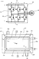
- a three-phase inverter circuit of the semiconductor module 10 is configured by those circuit element portions 11A, 11B, 11C. More specifically, the circuit element portions 11A, 11B, 11C are configured as a W phase circuit, V phase circuit, and U phase circuit forming a three-phase inverter circuit 40 shown in the circuit diagram in FIG. 3 .
- a three-phase AC motor 41 is connected to the three-phase inverter circuit 40.
- an IGBT element 12 which serves as a semiconductor element constituting an upper arm, and a free-wheel diode 13 connected reversely in parallel with the IGBT element 12, and an IGBT element 12, which constitutes a lower arm, and a free-wheel diode 13 connected reversely in parallel with the IGBT element 12 are mounted on an insulating substrate 14 attached to the heat radiation substrate 21.
- the circuit element portion 11B serving as the V phase circuit and the circuit element portion 11C serving as the U phase circuit have the configuration same as that of the circuit element portion 11A.
- a circuit pattern for configuring the abovementioned circuit is formed on each insulating substrate 14.
- the semiconductor module 10 is configured as a three-phase inverter circuit, but the semiconductor module 10 in accordance with the present invention is not limited to the three-phase inverter circuit configuration.
- the cooling device 20 is provided with the heat radiation substrate 21 shown in FIG. 1(a) , fins 22 shown in FIG. 2 , and a cooling case 23 shown in FIG. 1(b).
- FIG. 1(c) shows the rotated cooling case 23 shown in FIG. 1(b) .
- the fins 22 are formed integrally with the heat radiation substrate 21 on the surface of the heat radiation substrate 21 opposite that where the circuit element portions 11A, 11B, 11C are attached.
- the fins 22 are accommodated inside the cooling case 23.
- the cooling case 23 can be also referred to as a coolant jacket or a water jacket.
- FIG. 1(a) the insulating substrates 14 of the circuit element portions 11A, 11B, 11C are joined to the heat radiation substrate 21.
- the insulating substrates 14 and also the IGBT elements 12 and free-wheel diodes 13 carried on the insulating substrates 14 are thermoconductively connected to the cooling device 20.
- a metal layer to be used for joining to the heat radiation substrate 21 may be formed on each insulating substrate 14.
- a line cl in FIG. 1(a) is a central line, in the short-side direction, of the assembly of the fins 22 shown in FIG. 2 that are integrally attached to the heat radiation substrate 21.
- the fins 22 integrally attached to the heat radiation substrate 21 are used as a heat radiation plate, that is, the so-called heat sink.
- a heat radiation plate that is, the so-called heat sink.
- pin fins in which a plurality of pins of a square columnar shape (angular pins) shown in FIG. 2(a) is arranged at an interval with a predetermined pitch can be used as the fins 22.
- pin fins 22A in which a plurality of cylindrical pins (round pins) shown in FIG. 2(b) are arranged at an interval with a predetermined pitch can be also used.
- blade fins 22B in which a plurality of blade-shaped fins shown in FIG. 2(c) is provided parallel to each other can be also used.
- the pin fins 22, 22A shown in FIGS. 2(a) and 2(b) among the fins shown in FIGS. 2(a) to 2(c) , be used because such fins make it possible to increase the density of fins over that of the blade fins 22B shown in FIG. 2(c) .
- the angular pin fins 22 shown in FIG. 2(a) make it possible to increase the flow rate around the pins and also increase the surface area per one pin, thereby enabling the heat exchange with an efficiency higher than that attained with the round pin fins 22A shown in FIG. 2(b) .
- the angular pin fins 22 shown in FIG. 2(a) are considered as the representative fins.
- the shape and dimensions of the fins 22 are preferably set, as appropriate, with consideration for the conditions under which a cooling medium is introduced into the cooling device 20 (that is, pump performance and the like), type and properties (in particular, viscosity) of the cooling medium, and target heat removal amount. Further, the fins 22 are formed to a height such that a predetermined clearance is present between the tips of the fins 22 and the bottom wall of the cooling case 23 when the fins are accommodated in the cooling case 23.
- a region where the fins 22 are integrally attached to the heat radiation substrate 21 is preferably a region including a region obtained by projecting a region carrying the IGBT elements 12 and free-wheel diodes 13, which serve as semiconductor elements on the insulating substrate 14, in the thickness direction of the heat radiation substrate 21 in a state in which the heat radiation substrate 21 is joined to the insulating substrate 14.
- this region preferably includes the region directly below the IGBT elements 12 and free-wheel diodes 13.
- the assembly of the fins 22 is of a substantially rectangular parallelepiped, preferably rectangular parallelepiped, outer shape, and may have a chamfered or deformed shape, provided that the effect of the present invention is not lost.
- FIG. 2(a) shows the central line cl, in the lateral direction, of the assembly of the fins 22 having the rectangular parallelepiped outer shape.
- the cooling case 23 accommodating the fins 22 is of a box-like shape with an open upper portion which has a bottom wall 23a and a side wall 23b provided on the circumferential edge of the bottom wall 23a.
- the opening of the cooling case 23 is of a rectangular shape that matches the outer shape of the assembly of the fins 22.
- the cooling case 23 has a substantially rectangular parallelepiped outer shape, and the longitudinal direction thereof matches the longitudinal direction of the assembly of the fins 22.
- an introducing port 23c for introducing the cooling medium into the cooling case 23 is provided close to the corner of a first side wall 23b1, among the side walls 23b on the long side, and a discharge port 23d for discharging the cooling medium from the cooling case 23 to the outside is provided close to the corner of a second side wall 23b2, among the side walls 23b on the long side.
- the cooling medium introducing port 23c and discharge port 23d are provided in the first side wall 23b1 and the second side wall 23b2 at positions shifted in the mutually opposite directions from the central line cl, in the lateral direction, of the assembly of the fins 22.
- the heat radiation substrate 21 is attached to the cooling case 23
- an O-ring 23e is attached for preventing the cooling medium from leaking from the inside of the cooling case 23 when the cooling medium flows into the cooling case 23, and threaded holes 23f for screwing the heat radiation substrate 21 are formed in the four inner corners.
- the leak can be prevented by using a metal gasket or a liquid packing.
- a diffusion wall 23g which causes the cooling medium introduced from the introducing port 23c to diffuse along the first side wall 23b1, is provided between the first side wall 23b1 and the bottom wall 23a inside the cooling case 23 along the longitudinal direction of the cooling case 23.
- a converging wall 23h which causes the cooling medium to converge to the discharge port 23d along the second side wall 23b2, is provided inside the cooling case 23 between the second side wall 23b2 and the bottom wall 23a along the longitudinal direction of the cooling case 23.
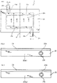
- FIG. 5 is a plan view taken when the heat radiation substrate 21 shown in FIG. 1(a) is attached to the cooling case 23 shown in FIG. 1(b) .
- FIG. 6 is a side view taken from the introducing port 23c side.
- FIG. 7 is a side view taken from the discharge port 23d side.
- FIG. 8 is a cross-sectional view taken along the A-A line in FIG. 5 .
- the circuit element portions 11A, 11B, 11C located on the heat radiation substrate 21 are omitted to facilitate the understanding of the present invention.
- the diffusion wall 23g is, in one example thereof, an ascending inclined surface formed from the bottom side of the first side wall 23b1 toward the bottom wall 23a.
- the converging wall 23h is, in one example thereof, a descending inclined surface formed from the bottom wall 23a toward the bottom side of the second side wall 23b2.
- the diffusion wall 23g and the converging wall 23h are inclined surfaces, vortexes that can occur when the diffusion wall 23g and the converging wall 23h are provided perpendicular to the introducing port 23c or the discharge port 23d can be suppressed. Further, by configuring the diffusion wall 23g and the converging wall 23h as simple inclined surfaces, it is possible to form the diffusion wall 23g and the converging wall 23h in an easy manner when the cooling case 23 is manufactured by die casting or the like.
- the angle of inclination of the diffusion wall 23g and the converging wall 23h with respect to the introducing port 23c or the discharge port 23d can be set by the span of this region.
- the span L of this region (see FIG. 4 ) is about 2 mm to 12 mm.
- the flow of the cooling medium which is shown by an arrow in FIG. 5 , is initially introduced from the introducing port 23c into the cooling case 23 where the flow collides with the diffusion wall 23g and diffuses along the diffusion wall 23g in the longitudinal direction inside the cooling case 23.
- the cooling medium then flows in a fin region 22e, in which the fins 22 are provided, in the lateral direction of the cooling case 23, in other words, in the lateral direction of the assembly of the fins 22, and exchanges heat with the heat sink. Then, the flow is converged along the converging wall 23h and discharged to the outside of the cooling case 23 from the discharge port 23d.
- the introducing port 23c and the discharge port 23d of the cooling case 23 are provided in the side wall 23b along the longitudinal direction of the cooling case 23, and the diffusion wall 23g is provided inside the cooling case 23.
- the cooling medium flows in the lateral direction of the assembly (rectangular parallelepiped shape) of the fins 22.
- the heat radiation ability can be increased by comparison with the case in which the cooling medium flows in the longitudinal direction of the assembly of the fins 22. The reason therefor is explained below.
- the density of the fins 22 is increased, high heat radiation ability can be obtained, but the pressure loss increases.
- the pressure loss increases over that when the cooling medium flows in the lateral direction. Accordingly, high heat radiation ability and a low pressure loss can be realized by allowing the cooling medium to flow in the lateral direction of the assembly of the fins 22 with respect to the fins 22 with a high arrangement density.
- the longitudinal direction of the assembly of the fins 22 is usually the same as the arrangement direction of those semiconductor elements.
- the cooling medium is allowed to flow in the longitudinal direction of the assembly of the fins 22
- the semiconductor elements on the downstream side in the flow direction of the cooling medium are cooled by the cooling medium warmed up by heat exchange with the semiconductor elements located on the upstream side, and the cooling effect is lower than that on the upstream side.
- the cooling medium is allowed to flow in the lateral direction of the assembly of the fins 22, as in the semiconductor device 1 of the present embodiment, the cooling medium flows in the direction orthogonal to the arrangement direction of a plurality of semiconductor elements (circuit element portions). Therefore, the unevenness of the cooling effect is reduced and the heat radiation ability can be increased, regardless of the arrangement position of the semiconductor element.
- the flow of the cooling medium flowing in the lateral direction of the assembly of the fins 22 is made uniform. This also results in the increased heat radiation ability.
- the effect of improving the uniformity of the cooling medium flow is particularly significant when the fins are in the form of angular pin fins 22 or round pin fins 22A and the pins are arranged with a high density to increase the heat radiation ability.
- the heat radiation ability can be further increased by the combined effect of the increase in the arrangement density of pins and improved uniformity of cooling medium flow.
- the arrangement density of the pins be increased such that the pin pitch, that is, the pin arrangement spacing (distance between the centers of adjacent pins) becomes equal to or less than about 4 mm.
- the pin pitch is within a range of 3 mm to 6 mm
- the heat radiation ability decreases with the increase in the pitch, but where the pitch is equal to or less than 4 mm, the increase in the temperature of semiconductor elements is about 5%, the coolant flow rate is raised and the heat radiation ability is increased, thereby enabling sufficient cooling.
- the pitch (spacing) of a plurality of adjacent pins constituting the pin fins be 1.25 times to 2 times the pin diameter.
- the pin diameter is the length of one side in the case of angular pins and the circle diameter in the case of round pins.
- the pin diameter is about 1 mm to 2 mm.
- the pitch is preferably within a range of 2.5 mm to 4 mm. This is because where the pitch is less than 2.5 mm, it is necessary to remove dust from the coolant or highly accurate machining should be performed, thereby increasing the cost.
- the inner diameter d (see FIG. 8 ) of the introducing port 23c be larger than the height h of the diffusion wall 23g. More specifically, when the inner diameter d of the introducing port 23c is 10 mm ⁇ to 15 mm ⁇ , the height of the diffusion wall 23g is preferably within a range of 0.1 mm to 13 mm. In the example shown in FIG. 8 , the inner diameter d of the introducing port 23c is equal to the inner diameter (tube diameter) of an introducing tube 23i connected to the introducing port 23c. At a larger inner diameter d of the introducing port 23c, that is, at a larger diameter of the introducing tube 23i, the pressure loss can be reduced.
- the diffusion wall 23g be provided to reduce the pressure loss in the introducing port 23c.
- the height h of the diffusion wall 23g is less than 0.1 mm, the effect of providing the diffusion wall 23g is low, and whether the height is above 13 mm, the pressure loss conversely increases.
- the height of the converging wall 23h can be made equal to the height h of the diffusion wall 23g. Thus, it is preferred that this height be within a range of 0.1 mm to 13 mm when the typical diameter of a discharge tube 23j connected to the discharge port 23d is 10 mm ⁇ to 15 mm ⁇ .
- the introducing port 23c and the discharge port 23d of the cooling case 23 are provided in side walls 23b (23b1, 23b2) along the longitudinal direction of the cooling case 23. Therefore, hoses can be easily attached to the introducing tube 23i and the discharge tube 23j. Further, since it is not necessary to provide an introducing port for introducing the cooling medium into the cooling case 23 or a discharge port for discharging the cooling medium in the bottom wall 23a of the cooling case 23, other electronic components can be further provided below the bottom wall 23a of the cooling case 23.
- the shape of the bottom wall 23a of the cooling case 23 is not particularly limited, provided that other electronic components can be disposed therebelow. Thus, the outer surface of the bottom wall 23a may be flat, as shown in FIG.
- the shape be used such that a recess is formed on the rear surface side of the bottom wall 23a of the cooling case 23 by the bottom wall 23a, diffusion wall 23g, and converging wall 23h, as shown in the cross-sectional view in FIG. 8 , because such a shape can reduce the cost of raw materials.
- the cooling case 23 has the same outer shape.
- the positions of the introducing port 23c and the discharge port 23d of the cooling case 23 are rotationally symmetrical with respect to the cooling case 23. Due to the rotational symmetry, the production of the cooling case 23 is facilitated.
- one of the openings formed in the side wall 23b may be freely determined as the introducing port 23c and the other as the discharge port 23d. As a result, handling is facilitated.
- FIG. 10 is a perspective view of the semiconductor device 1 of the embodiment in which a resin case 15 accommodating the semiconductor module 10 is attached to the circumferential edge of the heat radiation substrate 21 (not shown in the figure) on the cooling device 20.
- the resin case 15 shown in the figure has a substantially rectangular parallelepiped outer shape, and the dimensions thereof in the longitudinal and lateral directions, as viewed from above, are substantially the same as those of the cooling device 20.
- P-terminal and N-terminal 16 and U-terminal, V-terminal, and W-terminal 17 connected to the circuits of the semiconductor module 10 protrude at the upper surface of the resin case 15.
- the P-terminal and N-terminal 16 and U-terminal, V-terminal, and W-terminal 17 are provided along the longitudinal direction of the cooling case 23. At least one of those terminals 16, 17 can be provided along the lateral direction of the cooling case 23, but where a plurality of IGBT elements 12 and free-wheel diodes 13 is arranged in parallel as the circuit element portions 11A, 11B, 11C along the longitudinal direction of the heat radiation substrate 21, as shown in FIG. 1 , by providing the terminals 16, 17 along the longitudinal direction of the cooling case 23, it is possible to reduce the inductance between the terminals 16, 17 and the IGBT elements 12 (and also free-wheel diodes 13) by comparison with the case in which the terminals are provided along the lateral direction.
- the terminals 16, 17 along the longitudinal direction of the cooling case 23, it is possible to dispose a plurality of circuit element portions 11A, 11B, and 11C, which are provided with a plurality of IGBT elements 12 that are to be connected to those terminals, close to each other.
- the fins 22 that radiate the heat from the circuit element portions 11A, 11B, and 11C can be formed as a single assembly. Therefore, the production of the fins 22 is facilitated and the production cost of the fins 22 can be reduced.
- the introducing port 23c and the discharge port 23d of the cooling case 23 are provided at positions shifted in mutually opposite directions from the central line cl, in a lateral direction, of the assembly of the fins 22 at the first side wall 23b1 and the second side wall 23b2 of the cooling case 23. It is preferred that the introducing port 23c and the discharge port 23d of the cooling case 23 be provided with the P-terminal 16 and the N-terminal 16 therebetween.
- FIG. 11 shows the embodiment of the present invention in which a film capacitor 30 is provided below the cooling device 20.
- the resin case 15 accommodating the semiconductor module 10 inside thereof is provided above the cooling device 20.
- the terminals 16 connected to the circuit of the semiconductor module 10 protrude from the upper surface of the resin case 15.
- the terminals 16 and the terminals 31 of the film capacitor 30 provided below the cooling device 20 are connected to each other by bus bars 32.
- the introducing tube 23i connected to the introducing port 23c of the side wall 23b of the cooling case 23 of the cooling device 20 is provided at the end side with respect to the longitudinal position of the terminal 16 protruding from the resin case 15 of the semiconductor module 10 or the terminal 31 of the film capacitor 30.
- the bus bar 32 does not interfere with the introducing tube 23i, and the terminal 16 of the semiconductor module 10 and the terminal 31 of the film capacitor 30 are connected at the shortest possible distance.
- the introducing tube 23i shown in FIG. 11 may be also the discharge tube 23j.
- the material of the cooling case 23 should be selected from materials with a high thermal conductivity, or according to the structure when peripheral parts used during unit molding are involved. Where thermal conductivity is considered, materials such as A1050 and A6063 are preferred, and when sealing with peripheral members, in particular a fixing part or an inverter case accommodating a power module, is needed, materials such as ADC12 and A6061 are preferred.
- the cooling case 23 can be manufactured by die casting, and where thermal conductivity is needed, a material of a DMS series of aluminum alloys with a high thermal conductivity for die casting, which are manufactured by Mitsubishi Plastics, Inc., can be used.
- the introducing port 23c, the discharge port 23d, and the flow path inside the cooling case 23, such as described hereinabove, can be formed, for example, by die casting.
- a material obtained by including a carbon filler in a metal material can be used for the cooling case 23.
- a ceramic material or a resin material can be also used.
- Thermal analysis of the temperature of each IGBT element was performed with respect to the semiconductor device of the present embodiment, which constitutes the three-phase inverter circuit shown in FIG. 1 , as an example.
- thermal analysis of the temperature of each IGBT was performed with respect to a semiconductor device configured in the same manner as in the example, except that the introducing port and discharge port were provided in the side wall along the lateral direction of the cooling case and the cooling medium was allowed to flow in the longitudinal direction of the assembly of the fins 22.
- the analysis conditions in the example and comparative example were as follows.
- the cooling medium was water that included 50 vol% of a long-life coolant (LLC) and had a temperature of 65°C.
- the flow rate of the cooling medium was 10 L/min.
- the generation loss for each IGBT was taken as 360 W per 1 chip, the loss of FWD was taken as 45 W, and an inverter operation was presumed.
- the fins 22 were angular pins with a side of 2 mm, and the fin pitch was 3 mm.
- the pressure loss in the example was 5.8 kPa, and the pressure loss in the comparative example was 30 kPa.
- FIG. 12 is a graph showing the temperature of each IGBT element in the example and comparative example.
- WP to UN on the abscissa represent the positions of six IGBT elements.
- WP and WN show the IGBT elements of the upper arm and lower arm, respectively, in the W-phase circuit element portion 11A.
- VP and VN show the IGBT elements of the upper and lower arms in the V-phase circuit element portion 11B
- UP and UN show the IGBT elements of the upper and lower arms in the U-phase circuit element portion 11C. It follows from FIG. 12 that in the comparative example, the temperature of the IGBT element positioned on the downstream side in the flow direction of the cooling medium rises, whereas in the example, the IGBT elements have substantially the same temperature and excellent heat radiation ability is demonstrated.
- the typical diameter of the introducing tube 23i and the discharge tube 23j is 10 mm ⁇ to 15 mm ⁇ , and the tube diameter of 6 mm ⁇ and 9 mm ⁇ , which is shown in FIG. 13 , is less than the typical tube diameter.
- the pressure loss is higher than that with a tube diameter of 12 mm ⁇ , and the pressure loss increases with the height of the diffusion wall.
- the provided diffusion wall decreases the pressure loss by comparison with the case in which no diffusion wall is provided (the diffusion wall height is 0). This is apparently because by providing the diffusion wall, it is possible to reduce the pressure loss in the vicinity of the introducing port. It follows from FIG. 13 , that the effect of decreasing the pressure reduction by providing the diffusion wall is demonstrated as long as the diffusion wall is provided and this effect can be observed when the diffusion wall height is within a range below 13 mm (inclusive).
- the present invention is not limited to the abovementioned configuration and can be also applied to a semiconductor module including some semiconductor elements (circuit element portions) of different generation loss. Further, a plurality of circuit element portions may be formed on one insulating substrate.
- a semiconductor device comprises an insulating substrate, a semiconductor element carried on the insulating substrate, and a cooling device that cools the semiconductor element.
- the cooling device includes a heat radiation substrate joined to the insulating substrate, a plurality of fins provided in a substantially rectangular region on a surface of the heat radiation substrate on a side opposite that of a surface joined to the insulating substrate, and a cooling case of a box-like shape that accommodates the fins and has a bottom wall and side walls.
- the semiconductor device comprises an introducing port and a discharge port for a cooling medium are provided at positions shifted in mutually opposite directions from a laterally central line of an assembly of the fins in a pair of a first side wall and a second side wall provided along a longitudinal direction of the assembly of the fins, among the side walls of the cooling case.
- the semiconductor device comprises a diffusion wall causing the cooling medium introduced from the introducing port to diffuse along the first side wall is provided between the first side wall, in which the introducing port is provided, and the bottom wall.
- a converging wall causing the cooling medium to converge toward the discharge port along the second side wall is provided between the second side wall, in which the discharge port is provided, and the bottom wall.
- the diffusion wall is an ascending inclined surface formed from a bottom side of the first side wall toward the bottom wall.
- the converging wall is a descending inclined surface formed from the bottom wall toward a bottom side of the second side wall.
- the inner diameter of the introducing port is larger than the height of the diffusion wall.
- the inner diameter of the introducing port is 10 mm to 15 mm and the height of the diffusion wall is 0.1 mm to 13 mm.
- the positions of the introducing port and the discharger port are rotationally symmetrical with respect to the cooling case.
- a recess on a rear surface side of the bottom wall of the cooling case is formed by the bottom wall, the diffusion wall, and the converging wall.
- terminals of the semiconductor device are provided along the longitudinal direction of the cooling case.
- the fins are pin fins.
- the pin fins are constituted by a plurality of pins, and a pitch of the pins is 1.25 times to 2 times the pin diameter.
- a film capacitor is attached to the bottom wall of the cooling device.
Landscapes
- Engineering & Computer Science (AREA)
- Microelectronics & Electronic Packaging (AREA)
- Physics & Mathematics (AREA)
- Thermal Sciences (AREA)
- Cooling Or The Like Of Semiconductors Or Solid State Devices (AREA)
- Cooling Or The Like Of Electrical Apparatus (AREA)
- Inverter Devices (AREA)
Applications Claiming Priority (3)
| Application Number | Priority Date | Filing Date | Title |
|---|---|---|---|
| JP2012238284 | 2012-10-29 | ||
| EP13851646.3A EP2824703B1 (de) | 2012-10-29 | 2013-10-07 | Halbleiterbauelement |
| PCT/JP2013/077235 WO2014069174A1 (ja) | 2012-10-29 | 2013-10-07 | 半導体装置 |
Related Parent Applications (2)
| Application Number | Title | Priority Date | Filing Date |
|---|---|---|---|
| EP13851646.3A Division EP2824703B1 (de) | 2012-10-29 | 2013-10-07 | Halbleiterbauelement |
| EP13851646.3A Division-Into EP2824703B1 (de) | 2012-10-29 | 2013-10-07 | Halbleiterbauelement |
Publications (1)
| Publication Number | Publication Date |
|---|---|
| EP4064336A1 true EP4064336A1 (de) | 2022-09-28 |
Family
ID=50627090
Family Applications (2)
| Application Number | Title | Priority Date | Filing Date |
|---|---|---|---|
| EP22173123.5A Pending EP4064336A1 (de) | 2012-10-29 | 2013-10-07 | Halbleiterbauelement |
| EP13851646.3A Active EP2824703B1 (de) | 2012-10-29 | 2013-10-07 | Halbleiterbauelement |
Family Applications After (1)
| Application Number | Title | Priority Date | Filing Date |
|---|---|---|---|
| EP13851646.3A Active EP2824703B1 (de) | 2012-10-29 | 2013-10-07 | Halbleiterbauelement |
Country Status (5)
| Country | Link |
|---|---|
| US (1) | US10014236B2 (de) |
| EP (2) | EP4064336A1 (de) |
| JP (1) | JP5975110B2 (de) |
| CN (1) | CN104247010B (de) |
| WO (1) | WO2014069174A1 (de) |
Cited By (1)
| Publication number | Priority date | Publication date | Assignee | Title |
|---|---|---|---|---|
| US20230077047A1 (en) * | 2021-09-06 | 2023-03-09 | Nidec Corporation | Cooling device |
Families Citing this family (69)
| Publication number | Priority date | Publication date | Assignee | Title |
|---|---|---|---|---|
| US9337119B2 (en) * | 2014-07-14 | 2016-05-10 | Micron Technology, Inc. | Stacked semiconductor die assemblies with high efficiency thermal paths and associated systems |
| CN105940491B (zh) * | 2014-08-06 | 2019-06-25 | 富士电机株式会社 | 半导体装置 |
| DE102014111786A1 (de) * | 2014-08-19 | 2016-02-25 | Infineon Technologies Ag | Kühlplatte, Bauelement, das eine Kühlplatte umfasst, und Verfahren zum Herstellen einer Kühlplatte |
| KR101653453B1 (ko) * | 2014-11-03 | 2016-09-09 | 현대모비스 주식회사 | 전력반도체 양면 냉각방식 냉각장치 |
| JP6557962B2 (ja) * | 2014-11-14 | 2019-08-14 | 日産自動車株式会社 | 冷却器 |
| CN204335279U (zh) * | 2015-01-28 | 2015-05-13 | 讯凯国际股份有限公司 | 液体冷却式散热结构 |
| US10739084B2 (en) | 2015-01-28 | 2020-08-11 | Cooler Master Co., Ltd. | Liquid cooling heat sink structure and cooling circulation system thereof |
| WO2016187131A1 (en) * | 2015-05-15 | 2016-11-24 | Wolverine Tube, Inc. | Liquid cooled coldplate |
| US10509446B2 (en) | 2015-12-30 | 2019-12-17 | Cooler Master Co., Ltd. | Cooling apparatus for electronic components |
| JP6283379B2 (ja) * | 2016-01-29 | 2018-02-21 | 本田技研工業株式会社 | コンデンサの配置構造 |
| US12158786B2 (en) | 2016-02-15 | 2024-12-03 | Cooler Master Co., Ltd. | Cooling apparatus |
| US10409341B2 (en) | 2016-02-15 | 2019-09-10 | Cooler Master Co., Ltd. | Cooling apparatus |
| US12099385B2 (en) | 2016-02-15 | 2024-09-24 | Cooler Master Co., Ltd. | Cooling apparatus |
| US20190086157A1 (en) * | 2016-03-04 | 2019-03-21 | Nec Corporation | Cooling system, cooler, and cooling method |
| TWI635248B (zh) * | 2016-09-02 | 2018-09-11 | 宏碁股份有限公司 | 蒸發器及其製作方法 |
| KR200494468Y1 (ko) * | 2017-02-23 | 2021-10-18 | 엘에스일렉트릭(주) | 모듈형 냉각장치를 이용한 방열 시스템 |
| US10850623B2 (en) | 2017-10-30 | 2020-12-01 | Sf Motors, Inc. | Stacked electric vehicle inverter cells |
| JP6663899B2 (ja) * | 2017-11-29 | 2020-03-13 | 本田技研工業株式会社 | 冷却装置 |
| US10790758B2 (en) | 2018-03-08 | 2020-09-29 | Chongqing Jinkang New Energy Vehicle Co., Ltd. | Power converter for electric vehicle drive systems |
| JP6563161B1 (ja) * | 2018-03-15 | 2019-08-21 | 三菱電機株式会社 | 冷却器、電力変換装置ユニット及び冷却システム |
| WO2019176620A1 (ja) * | 2018-03-15 | 2019-09-19 | 三菱電機株式会社 | 冷却器、電力変換装置ユニット及び冷却システム |
| US10779445B2 (en) | 2018-03-23 | 2020-09-15 | Chongqing Jinkang New Energy Vehicle Co., Ltd. | Inverter module having multiple half-bridge modules for a power converter of an electric vehicle |
| US10756649B2 (en) | 2018-03-23 | 2020-08-25 | Chongqing Jinkang New Energy Vehicle Co., Ltd. | Inverter module having multiple half-bridge modules for a power converter of an electric vehicle |
| US10236791B1 (en) | 2018-03-23 | 2019-03-19 | Sf Motors, Inc. | Inverter module having multiple half-bridge modules for a power converter of an electric vehicle |
| JP7205071B2 (ja) * | 2018-04-02 | 2023-01-17 | 富士電機株式会社 | 冷却装置、半導体モジュールおよび車両 |
| US10778117B2 (en) | 2018-04-17 | 2020-09-15 | Chongqing Jinkang New Energy Vehicle Co., Ltd. | Inverter module of an electric vehicle |
| US10772242B2 (en) | 2018-04-17 | 2020-09-08 | Chongqing Jinkang New Energy Vehicle Co., Ltd. | Inverter module of an electric vehicle |
| US10600577B2 (en) | 2018-04-26 | 2020-03-24 | Sf Motors, Inc. | Electric vehicle inverter module capacitors |
| US10660242B2 (en) | 2018-04-26 | 2020-05-19 | Chongqing Jinkang New Energy Vehicle Co., Ltd. | Electric vehicle inverter module heat sink |
| US10608423B2 (en) | 2018-04-26 | 2020-03-31 | Sf Motors, Inc. | Electric vehicle inverter module laminated bus bar |
| US10600578B2 (en) | 2018-04-26 | 2020-03-24 | Sf Motors, Inc. | Electric vehicle inverter module capacitors |
| EP3564992B1 (de) * | 2018-05-02 | 2021-07-07 | EKWB d.o.o. | Fluidbasierte kühlvorrichtung zum kühlen von mindestens zwei verschiedenen ersten wärmeerzeugenden elementen einer wärmequellenanordnung |
| EP3761356B1 (de) * | 2018-10-03 | 2024-07-10 | Fuji Electric Co., Ltd. | Halbleiterapparat |
| EP3761361B1 (de) * | 2018-10-05 | 2024-08-21 | Fuji Electric Co., Ltd. | Halbleiterbauelement, halbleitermodul und fahrzeug |
| FR3087617B1 (fr) * | 2018-10-17 | 2023-10-27 | Valeo Systemes De Controle Moteur | Equipement electronique pour vehicule |
| JP6887688B2 (ja) * | 2019-02-07 | 2021-06-16 | 株式会社高純度化学研究所 | 蒸発原料用容器、及びその蒸発原料用容器を用いた固体気化供給システム |
| JP6901153B2 (ja) * | 2019-02-07 | 2021-07-14 | 株式会社高純度化学研究所 | 薄膜形成用金属ハロゲン化合物の固体気化供給システム。 |
| JP7243262B2 (ja) * | 2019-02-15 | 2023-03-22 | 富士電機株式会社 | 半導体モジュール、車両および製造方法 |
| JP6789335B2 (ja) * | 2019-03-05 | 2020-11-25 | 三菱電機株式会社 | ヒートシンク及びこれを備えた半導体モジュール |
| US10975876B2 (en) | 2019-04-19 | 2021-04-13 | Cooler Master Co., Ltd. | Cooling device |
| JP7334464B2 (ja) * | 2019-05-15 | 2023-08-29 | 富士電機株式会社 | 半導体モジュール、半導体モジュールの製造方法および段差冶具 |
| CN113892172B (zh) * | 2019-05-30 | 2025-01-14 | 三菱电机株式会社 | 半导体装置 |
| FR3097094B1 (fr) * | 2019-06-06 | 2022-09-09 | Valeo Siemens Eautomotive France Sas | Circuit de refroidissement actif pour équipement électrique |
| JP6815451B1 (ja) * | 2019-08-23 | 2021-01-20 | 三菱電機株式会社 | インバータ装置 |
| US11217505B2 (en) * | 2019-09-10 | 2022-01-04 | Aptiv Technologies Limited | Heat exchanger for electronics |
| TWI703271B (zh) | 2019-10-07 | 2020-09-01 | 訊凱國際股份有限公司 | 發光風扇裝置與非發光風扇裝置 |
| US11460036B2 (en) | 2019-10-07 | 2022-10-04 | Cooler Master Co., Ltd. | Light emitting fan device and non-light emitting fan device |
| JP6874823B1 (ja) * | 2019-12-26 | 2021-05-19 | 株式会社明電舎 | 冷却構造及びヒートシンク |
| US11134590B2 (en) | 2020-01-13 | 2021-09-28 | Ford Global Technologies, Llc | Automotive power inverter with cooling channels and cooling pins |
| JP7205662B2 (ja) * | 2020-03-18 | 2023-01-17 | 富士電機株式会社 | 半導体モジュール |
| CN111740565A (zh) * | 2020-07-22 | 2020-10-02 | 新风光电子科技股份有限公司 | 一种级联逆变器一体式水冷装置 |
| JP7388319B2 (ja) * | 2020-09-02 | 2023-11-29 | 株式会社デンソー | 電力変換装置 |
| JP7577953B2 (ja) * | 2020-09-17 | 2024-11-06 | 富士電機株式会社 | 半導体装置及び半導体装置の製造方法 |
| DE102020213629A1 (de) * | 2020-10-29 | 2022-05-05 | Valeo Siemens Eautomotive Germany Gmbh | Leistungsmodul und leistungselektronisches Gerät |
| EP4006968B1 (de) | 2020-11-26 | 2023-03-22 | Hitachi Energy Switzerland AG | Leistungshalbleiterbauelement |
| JP7622410B2 (ja) * | 2020-12-01 | 2025-01-28 | 富士電機株式会社 | 冷却器及び半導体装置 |
| KR102862230B1 (ko) * | 2021-01-28 | 2025-09-19 | 엘에스일렉트릭(주) | 전력기기용 히트싱크 |
| JP7628845B2 (ja) * | 2021-03-16 | 2025-02-12 | 株式会社デンソー | 電力変換装置 |
| US20220352051A1 (en) * | 2021-04-28 | 2022-11-03 | Nidec Corporation | Heat dissipation member and cooling device |
| FR3122801B1 (fr) * | 2021-05-10 | 2023-08-04 | Valeo Systemes De Controle Moteur | Système de conversion de tension et procédé de fabrication d’un tel système de conversion de tension |
| JP2023023518A (ja) * | 2021-08-05 | 2023-02-16 | 日本電産株式会社 | 液冷ジャケット、および冷却装置 |
| JP2023023517A (ja) * | 2021-08-05 | 2023-02-16 | 日本電産株式会社 | 液冷ジャケット、および冷却装置 |
| DE102021214226A1 (de) * | 2021-12-13 | 2023-06-15 | Robert Bosch Gesellschaft mit beschränkter Haftung | Kühlkörper zur Kühlung einer elektrischen und/oder elektronischen Baugruppe |
| JP2023096940A (ja) * | 2021-12-27 | 2023-07-07 | ニデック株式会社 | 放熱部材および冷却装置 |
| JP7111268B1 (ja) * | 2022-01-19 | 2022-08-02 | 富士電機株式会社 | 冷却器及び半導体装置 |
| JP7777029B2 (ja) | 2022-03-31 | 2025-11-27 | 本田技研工業株式会社 | ウォータージャケット |
| EP4459674A4 (de) * | 2022-08-24 | 2025-07-30 | Fuji Electric Co Ltd | Halbleiteranordnung |
| JP2026054049A (ja) | 2024-09-13 | 2026-03-26 | 富士電機株式会社 | 冷却器 |
| DE102025134039A1 (de) | 2024-09-24 | 2026-03-26 | Fuji Electric Co., Ltd. | Kühler |
Citations (8)
| Publication number | Priority date | Publication date | Assignee | Title |
|---|---|---|---|---|
| JP2001308246A (ja) | 2000-02-16 | 2001-11-02 | Hitachi Ltd | 電力変換装置 |
| US20040173392A1 (en) * | 2002-04-18 | 2004-09-09 | Hitachi, Ltd. | Electrical apparatus, cooling system therefor, and electric vehicle |
| JP2005019905A (ja) | 2003-06-30 | 2005-01-20 | Matsushita Electric Ind Co Ltd | 冷却装置 |
| JP2007123607A (ja) | 2005-10-28 | 2007-05-17 | Toyota Motor Corp | 電気機器の冷却構造 |
| JP2007294891A (ja) | 2006-03-30 | 2007-11-08 | Dowa Metaltech Kk | 放熱器 |
| JP2011103369A (ja) | 2009-11-11 | 2011-05-26 | Nippon Inter Electronics Corp | パワー半導体モジュール及びその製造方法 |
| EP2711983A1 (de) * | 2011-05-16 | 2014-03-26 | Fuji Electric Co., Ltd. | Kühler zur verwendung in einem halbleitermodul |
| EP2840604A1 (de) * | 2012-04-16 | 2015-02-25 | Fuji Electric Co., Ltd. | Halbleiterbauelement und kühler für ein halbleiterbauelement |
Family Cites Families (37)
| Publication number | Priority date | Publication date | Assignee | Title |
|---|---|---|---|---|
| US4884630A (en) * | 1988-07-14 | 1989-12-05 | Microelectronics And Computer Technology Corporation | End fed liquid heat exchanger for an electronic component |
| JP2001035981A (ja) * | 1999-07-16 | 2001-02-09 | Toshiba Corp | 半導体素子用冷却器及びこれを用いた電力変換装置 |
| US6414867B2 (en) * | 2000-02-16 | 2002-07-02 | Hitachi, Ltd. | Power inverter |
| JP2002098454A (ja) * | 2000-07-21 | 2002-04-05 | Mitsubishi Materials Corp | 液冷ヒートシンク及びその製造方法 |
| US7156159B2 (en) * | 2003-03-17 | 2007-01-02 | Cooligy, Inc. | Multi-level microchannel heat exchangers |
| JP4014549B2 (ja) * | 2003-09-18 | 2007-11-28 | 富士電機システムズ株式会社 | ヒートシンク及びその製造方法 |
| DE602005006310T2 (de) * | 2004-11-24 | 2009-05-20 | Danfoss Silicon Power Gmbh | Durchflussverteilungsmodul und Stapel von Durchflussverteilungsmodulen |
| US7301770B2 (en) * | 2004-12-10 | 2007-11-27 | International Business Machines Corporation | Cooling apparatus, cooled electronic module, and methods of fabrication thereof employing thermally conductive, wire-bonded pin fins |
| US20090065178A1 (en) * | 2005-04-21 | 2009-03-12 | Nippon Light Metal Company, Ltd. | Liquid cooling jacket |
| JP2006310363A (ja) * | 2005-04-26 | 2006-11-09 | Toshiba Corp | パワー半導体装置 |
| US8030754B2 (en) * | 2007-01-31 | 2011-10-04 | Hewlett-Packard Development Company, L.P. | Chip cooling channels formed in wafer bonding gap |
| TWM323069U (en) * | 2007-06-06 | 2007-12-01 | Man Zai Ind Co Ltd | Liquid-cooling heat-absorbing device |
| EP2234153B1 (de) * | 2007-11-26 | 2019-07-03 | Showa Denko K.K. | Flüssiggekühlte kühleinrichtung |
| US20090145581A1 (en) * | 2007-12-11 | 2009-06-11 | Paul Hoffman | Non-linear fin heat sink |
| US9671179B2 (en) * | 2008-01-15 | 2017-06-06 | Showa Denko K.K. | Liquid-cooled-type cooling device |
| JP4657329B2 (ja) * | 2008-07-29 | 2011-03-23 | 日立オートモティブシステムズ株式会社 | 電力変換装置および電動車両 |
| JP5061065B2 (ja) * | 2008-08-26 | 2012-10-31 | 株式会社豊田自動織機 | 液冷式冷却装置 |
| US20100078155A1 (en) * | 2008-09-30 | 2010-04-01 | Third Millennium Engineering | Thin Cavity Fluidic Heat Exchanger |
| JP2010123881A (ja) * | 2008-11-21 | 2010-06-03 | Fujikura Ltd | コールドプレート |
| JP5381561B2 (ja) * | 2008-11-28 | 2014-01-08 | 富士電機株式会社 | 半導体冷却装置 |
| KR101729254B1 (ko) * | 2009-08-07 | 2017-04-24 | 가부시키가이샤 유에이씨제이 | 히트 싱크 |
| EP2465138B1 (de) * | 2009-08-10 | 2016-11-23 | Fuji Electric Co., Ltd. | Halbleitermodul und kühleinheit |
| JP5702988B2 (ja) * | 2010-01-29 | 2015-04-15 | 株式会社 日立パワーデバイス | 半導体パワーモジュール及びそれが搭載される電力変換装置並びに半導体パワーモジュール搭載用水路形成体の製造方法 |
| JP5565459B2 (ja) * | 2010-04-21 | 2014-08-06 | 富士電機株式会社 | 半導体モジュール及び冷却器 |
| JP5533215B2 (ja) * | 2010-05-10 | 2014-06-25 | 富士通株式会社 | 冷却ジャケット及びそれを備えた電子機器 |
| JP5813300B2 (ja) * | 2010-08-23 | 2015-11-17 | 三桜工業株式会社 | 冷却装置 |
| US20120168128A1 (en) * | 2011-01-05 | 2012-07-05 | Kambiz Vafai | Cooling augmentation using microchannels with rotatable separating plates |
| US8804339B2 (en) * | 2011-02-28 | 2014-08-12 | Toyota Motor Engineering & Manufacturing North America, Inc. | Power electronics assemblies, insulated metal substrate assemblies, and vehicles incorporating the same |
| EP2704191B1 (de) * | 2011-04-26 | 2019-03-13 | Fuji Electric Co., Ltd. | Kühler für ein halbleitermodul |
| US9818670B2 (en) * | 2011-07-29 | 2017-11-14 | Infinera Corporation | Cooling device installation using a retainer assembly |
| US8963321B2 (en) * | 2011-09-12 | 2015-02-24 | Infineon Technologies Ag | Semiconductor device including cladded base plate |
| US8519532B2 (en) * | 2011-09-12 | 2013-08-27 | Infineon Technologies Ag | Semiconductor device including cladded base plate |
| KR101906645B1 (ko) * | 2011-10-12 | 2018-10-10 | 후지 덴키 가부시키가이샤 | 반도체 모듈용 냉각기 및 반도체 모듈 |
| US9425124B2 (en) * | 2012-02-02 | 2016-08-23 | International Business Machines Corporation | Compliant pin fin heat sink and methods |
| US8699226B2 (en) * | 2012-04-03 | 2014-04-15 | Google Inc. | Active cooling debris bypass fin pack |
| JP2013247354A (ja) * | 2012-05-23 | 2013-12-09 | Samsung Electro-Mechanics Co Ltd | 電力モジュール用放熱システム |
| KR101608182B1 (ko) * | 2012-08-02 | 2016-03-31 | 미쓰비시덴키 가부시키가이샤 | 방열판 |
-
2013
- 2013-10-07 WO PCT/JP2013/077235 patent/WO2014069174A1/ja not_active Ceased
- 2013-10-07 EP EP22173123.5A patent/EP4064336A1/de active Pending
- 2013-10-07 EP EP13851646.3A patent/EP2824703B1/de active Active
- 2013-10-07 CN CN201380019990.7A patent/CN104247010B/zh active Active
- 2013-10-07 JP JP2014544397A patent/JP5975110B2/ja active Active
-
2014
- 2014-10-10 US US14/511,734 patent/US10014236B2/en active Active
Patent Citations (9)
| Publication number | Priority date | Publication date | Assignee | Title |
|---|---|---|---|---|
| JP2001308246A (ja) | 2000-02-16 | 2001-11-02 | Hitachi Ltd | 電力変換装置 |
| US20040173392A1 (en) * | 2002-04-18 | 2004-09-09 | Hitachi, Ltd. | Electrical apparatus, cooling system therefor, and electric vehicle |
| JP2005019905A (ja) | 2003-06-30 | 2005-01-20 | Matsushita Electric Ind Co Ltd | 冷却装置 |
| JP2007123607A (ja) | 2005-10-28 | 2007-05-17 | Toyota Motor Corp | 電気機器の冷却構造 |
| DE112006002839T5 (de) * | 2005-10-28 | 2008-09-18 | Toyota Jidosha Kabushiki Kaisha, Toyota | Kühlstruktur für eine elektrische Vorrichtung |
| JP2007294891A (ja) | 2006-03-30 | 2007-11-08 | Dowa Metaltech Kk | 放熱器 |
| JP2011103369A (ja) | 2009-11-11 | 2011-05-26 | Nippon Inter Electronics Corp | パワー半導体モジュール及びその製造方法 |
| EP2711983A1 (de) * | 2011-05-16 | 2014-03-26 | Fuji Electric Co., Ltd. | Kühler zur verwendung in einem halbleitermodul |
| EP2840604A1 (de) * | 2012-04-16 | 2015-02-25 | Fuji Electric Co., Ltd. | Halbleiterbauelement und kühler für ein halbleiterbauelement |
Cited By (2)
| Publication number | Priority date | Publication date | Assignee | Title |
|---|---|---|---|---|
| US20230077047A1 (en) * | 2021-09-06 | 2023-03-09 | Nidec Corporation | Cooling device |
| US12158313B2 (en) * | 2021-09-06 | 2024-12-03 | Nidec Corporation | Cooling device |
Also Published As
| Publication number | Publication date |
|---|---|
| US20150021756A1 (en) | 2015-01-22 |
| US10014236B2 (en) | 2018-07-03 |
| WO2014069174A1 (ja) | 2014-05-08 |
| EP2824703A4 (de) | 2016-01-27 |
| JPWO2014069174A1 (ja) | 2016-09-08 |
| EP2824703B1 (de) | 2022-06-29 |
| EP2824703A1 (de) | 2015-01-14 |
| CN104247010B (zh) | 2017-06-20 |
| JP5975110B2 (ja) | 2016-08-23 |
| CN104247010A (zh) | 2014-12-24 |
Similar Documents
| Publication | Publication Date | Title |
|---|---|---|
| EP2824703B1 (de) | Halbleiterbauelement | |
| US9673130B2 (en) | Semiconductor device having a cooler | |
| US9502329B2 (en) | Semiconductor module cooler | |
| US8243451B2 (en) | Cooling member for heat containing device | |
| CN103839904B (zh) | 功率转换装置 | |
| CN104247009A (zh) | 半导体装置以及半导体装置的制造方法 | |
| WO2013157467A1 (ja) | 半導体装置および半導体装置用冷却器 | |
| CN111937141B (zh) | 半导体装置 | |
| JP7160216B2 (ja) | 半導体装置 | |
| US20220295672A1 (en) | Power conversion device and manufacturing method therefor | |
| JP2004080856A (ja) | 電力変換装置 | |
| JP2008218828A (ja) | 冷却装置及び冷却装置付半導体装置 | |
| CN219759575U (zh) | 散热结构及功率半导体器件模块 | |
| EP4546411A2 (de) | Halbleiteranordnung | |
| US20240379499A1 (en) | Cooler and semiconductor device | |
| JP2023103785A (ja) | 半導体装置 | |
| JP2016058427A (ja) | 冷却器 | |
| JP2011151193A (ja) | 冷却器 |
Legal Events
| Date | Code | Title | Description |
|---|---|---|---|
| PUAI | Public reference made under article 153(3) epc to a published international application that has entered the european phase |
Free format text: ORIGINAL CODE: 0009012 |
|
| STAA | Information on the status of an ep patent application or granted ep patent |
Free format text: STATUS: REQUEST FOR EXAMINATION WAS MADE |
|
| 17P | Request for examination filed |
Effective date: 20220512 |
|
| AC | Divisional application: reference to earlier application |
Ref document number: 2824703 Country of ref document: EP Kind code of ref document: P |
|
| AK | Designated contracting states |
Kind code of ref document: A1 Designated state(s): AL AT BE BG CH CY CZ DE DK EE ES FI FR GB GR HR HU IE IS IT LI LT LU LV MC MK MT NL NO PL PT RO RS SE SI SK SM TR |
|
| STAA | Information on the status of an ep patent application or granted ep patent |
Free format text: STATUS: EXAMINATION IS IN PROGRESS |
|
| 17Q | First examination report despatched |
Effective date: 20251014 |