EP4030620A1 - Hybrid bulk acoustic wave filter - Google Patents
Hybrid bulk acoustic wave filter Download PDFInfo
- Publication number
- EP4030620A1 EP4030620A1 EP22150239.6A EP22150239A EP4030620A1 EP 4030620 A1 EP4030620 A1 EP 4030620A1 EP 22150239 A EP22150239 A EP 22150239A EP 4030620 A1 EP4030620 A1 EP 4030620A1
- Authority
- EP
- European Patent Office
- Prior art keywords
- acoustic
- acoustic resonators
- piezoelectric material
- filtering circuitry
- node
- Prior art date
- Legal status (The legal status is an assumption and is not a legal conclusion. Google has not performed a legal analysis and makes no representation as to the accuracy of the status listed.)
- Pending
Links
Images


Classifications
-
- H—ELECTRICITY
- H03—ELECTRONIC CIRCUITRY
- H03H—IMPEDANCE NETWORKS, e.g. RESONANT CIRCUITS; RESONATORS
- H03H9/00—Networks comprising electromechanical or electro-acoustic elements; Electromechanical resonators
- H03H9/02—Details
- H03H9/02007—Details of bulk acoustic wave devices
- H03H9/02015—Characteristics of piezoelectric layers, e.g. cutting angles
-
- H—ELECTRICITY
- H03—ELECTRONIC CIRCUITRY
- H03H—IMPEDANCE NETWORKS, e.g. RESONANT CIRCUITS; RESONATORS
- H03H9/00—Networks comprising electromechanical or electro-acoustic elements; Electromechanical resonators
- H03H9/46—Filters
- H03H9/54—Filters comprising resonators of piezoelectric or electrostrictive material
- H03H9/56—Monolithic crystal filters
- H03H9/566—Electric coupling means therefor
- H03H9/568—Electric coupling means therefor consisting of a ladder configuration
-
- H—ELECTRICITY
- H03—ELECTRONIC CIRCUITRY
- H03H—IMPEDANCE NETWORKS, e.g. RESONANT CIRCUITS; RESONATORS
- H03H9/00—Networks comprising electromechanical or electro-acoustic elements; Electromechanical resonators
- H03H9/0004—Impedance-matching networks
- H03H9/0014—Impedance-matching networks using bulk acoustic wave devices
-
- H—ELECTRICITY
- H03—ELECTRONIC CIRCUITRY
- H03H—IMPEDANCE NETWORKS, e.g. RESONANT CIRCUITS; RESONATORS
- H03H9/00—Networks comprising electromechanical or electro-acoustic elements; Electromechanical resonators
- H03H9/02—Details
- H03H9/02007—Details of bulk acoustic wave devices
- H03H9/02015—Characteristics of piezoelectric layers, e.g. cutting angles
- H03H9/02031—Characteristics of piezoelectric layers, e.g. cutting angles consisting of ceramic
-
- H—ELECTRICITY
- H03—ELECTRONIC CIRCUITRY
- H03H—IMPEDANCE NETWORKS, e.g. RESONANT CIRCUITS; RESONATORS
- H03H9/00—Networks comprising electromechanical or electro-acoustic elements; Electromechanical resonators
- H03H9/02—Details
- H03H9/02535—Details of surface acoustic wave devices
- H03H9/02543—Characteristics of substrate, e.g. cutting angles
-
- H—ELECTRICITY
- H03—ELECTRONIC CIRCUITRY
- H03H—IMPEDANCE NETWORKS, e.g. RESONANT CIRCUITS; RESONATORS
- H03H9/00—Networks comprising electromechanical or electro-acoustic elements; Electromechanical resonators
- H03H9/15—Constructional features of resonators consisting of piezoelectric or electrostrictive material
- H03H9/17—Constructional features of resonators consisting of piezoelectric or electrostrictive material having a single resonator
- H03H9/171—Constructional features of resonators consisting of piezoelectric or electrostrictive material having a single resonator implemented with thin-film techniques, i.e. of the film bulk acoustic resonator [FBAR] type
- H03H9/172—Means for mounting on a substrate, i.e. means constituting the material interface confining the waves to a volume
- H03H9/173—Air-gaps
-
- H—ELECTRICITY
- H03—ELECTRONIC CIRCUITRY
- H03H—IMPEDANCE NETWORKS, e.g. RESONANT CIRCUITS; RESONATORS
- H03H9/00—Networks comprising electromechanical or electro-acoustic elements; Electromechanical resonators
- H03H9/15—Constructional features of resonators consisting of piezoelectric or electrostrictive material
- H03H9/17—Constructional features of resonators consisting of piezoelectric or electrostrictive material having a single resonator
- H03H9/171—Constructional features of resonators consisting of piezoelectric or electrostrictive material having a single resonator implemented with thin-film techniques, i.e. of the film bulk acoustic resonator [FBAR] type
- H03H9/172—Means for mounting on a substrate, i.e. means constituting the material interface confining the waves to a volume
- H03H9/174—Membranes
-
- H—ELECTRICITY
- H03—ELECTRONIC CIRCUITRY
- H03H—IMPEDANCE NETWORKS, e.g. RESONANT CIRCUITS; RESONATORS
- H03H9/00—Networks comprising electromechanical or electro-acoustic elements; Electromechanical resonators
- H03H9/15—Constructional features of resonators consisting of piezoelectric or electrostrictive material
- H03H9/17—Constructional features of resonators consisting of piezoelectric or electrostrictive material having a single resonator
- H03H9/176—Constructional features of resonators consisting of piezoelectric or electrostrictive material having a single resonator consisting of ceramic material
-
- H—ELECTRICITY
- H03—ELECTRONIC CIRCUITRY
- H03H—IMPEDANCE NETWORKS, e.g. RESONANT CIRCUITS; RESONATORS
- H03H9/00—Networks comprising electromechanical or electro-acoustic elements; Electromechanical resonators
- H03H9/46—Filters
- H03H9/54—Filters comprising resonators of piezoelectric or electrostrictive material
- H03H9/542—Filters comprising resonators of piezoelectric or electrostrictive material including passive elements
-
- H—ELECTRICITY
- H03—ELECTRONIC CIRCUITRY
- H03H—IMPEDANCE NETWORKS, e.g. RESONANT CIRCUITS; RESONATORS
- H03H9/00—Networks comprising electromechanical or electro-acoustic elements; Electromechanical resonators
- H03H9/46—Filters
- H03H9/54—Filters comprising resonators of piezoelectric or electrostrictive material
- H03H9/56—Monolithic crystal filters
- H03H9/562—Monolithic crystal filters comprising a ceramic piezoelectric layer
-
- H—ELECTRICITY
- H03—ELECTRONIC CIRCUITRY
- H03H—IMPEDANCE NETWORKS, e.g. RESONANT CIRCUITS; RESONATORS
- H03H9/00—Networks comprising electromechanical or electro-acoustic elements; Electromechanical resonators
- H03H9/46—Filters
- H03H9/54—Filters comprising resonators of piezoelectric or electrostrictive material
- H03H9/56—Monolithic crystal filters
- H03H9/564—Monolithic crystal filters implemented with thin-film techniques
-
- H—ELECTRICITY
- H03—ELECTRONIC CIRCUITRY
- H03H—IMPEDANCE NETWORKS, e.g. RESONANT CIRCUITS; RESONATORS
- H03H9/00—Networks comprising electromechanical or electro-acoustic elements; Electromechanical resonators
- H03H9/46—Filters
- H03H9/54—Filters comprising resonators of piezoelectric or electrostrictive material
- H03H9/58—Multiple crystal filters
- H03H9/60—Electric coupling means therefor
- H03H9/605—Electric coupling means therefor consisting of a ladder configuration
-
- H—ELECTRICITY
- H03—ELECTRONIC CIRCUITRY
- H03H—IMPEDANCE NETWORKS, e.g. RESONANT CIRCUITS; RESONATORS
- H03H9/00—Networks comprising electromechanical or electro-acoustic elements; Electromechanical resonators
- H03H9/70—Multiple-port networks for connecting several sources or loads, working on different frequencies or frequency bands, to a common load or source
- H03H9/703—Networks using bulk acoustic wave devices
- H03H9/706—Duplexers
Definitions
- the present disclosure relates to filtering circuitry for radio frequency (RF) signals, and specifically the filtering circuitry for RF signals including bulk acoustic wave (BAW) resonators.
- RF radio frequency
- BAW bulk acoustic wave
- acoustic wave devices are widely used in modern electronics.
- acoustic wave devices include a piezoelectric material in contact with one or more electrodes. Piezoelectric materials acquire a charge when compressed, twisted, or distorted, and similarly compress, twist, or distort when a charge is applied to them. Accordingly, when an alternating electrical signal is applied to the one or more electrodes in contact with the piezoelectric material, a corresponding mechanical signal (i.e., an oscillation or vibration) is transduced therein.
- the mechanical signal transduced in the piezoelectric material exhibits a frequency dependence on the alternating electrical signal.
- Acoustic wave devices leverage this frequency dependence to provide one or more functions, such as filtering.
- Exemplary acoustic wave devices include BAW resonators, which are increasingly used to form filters used in the transmission and reception of RF signals for communication. Due to the stringent demands placed on filters for modern RF communication systems such as the specifications for fifth generation (5G) wireless networks, acoustic wave devices for these applications must provide high quality factor and high bandwidth (which can be achieved by high electromechanical coupling).
- BAW resonators which are increasingly used to form filters used in the transmission and reception of RF signals for communication. Due to the stringent demands placed on filters for modern RF communication systems such as the specifications for fifth generation (5G) wireless networks, acoustic wave devices for these applications must provide high quality factor and high bandwidth (which can be achieved by high electromechanical coupling).
- RF filtering circuitry comprises a first node, a second node, and a series signal path between the first node and the second node.
- a number of acoustic resonators are coupled to the first node and the second node via the series signal path.
- a first one of the acoustic resonators is associated with a first quality factor and a first electromechanical coupling coefficient.
- a second one of the acoustic resonators is associated with a second quality factor and a second electromechanical coupling coefficient. The first quality factor is different from the second quality factor and the first electromechanical coupling coefficient is different from the second electromechanical coupling coefficient.
- a better balance between performance parameters such as electromechanical coupling (and thus bandwidth) and quality factor may be achieved for the RF filtering circuitry.
- Each one of the acoustic resonators may include a first electrode, a piezoelectric layer on the first electrode, and a second electrode on the piezoelectric layer such that the piezoelectric layer is between the first electrode and the second electrode.
- the piezoelectric material of the first one of the acoustic resonators may be different from the piezoelectric material of the second one of the acoustic resonators.
- the first one of the acoustic resonators may include a piezoelectric layer comprising a first piezoelectric material and the second one of the acoustic resonators may include a piezoelectric layer comprising a second piezoelectric material.
- the first piezoelectric material comprises intrinsic aluminum nitride and the second piezoelectric material comprises aluminum nitride doped with scandium.
- the first piezoelectric material comprises aluminum nitride doped with scandium at a first doping concentration and the second piezoelectric material comprises aluminum nitride doped with scandium at a second doping concentration that is greater than the first doping concentration.
- FIG. 1A illustrates an acoustic resonator 10 according to one embodiment of the present disclosure.
- the acoustic resonator 10 includes a substrate 12, a reflector 14 on the substrate, the reflector 14 including a number of reflector layers 16 that alternate in their material characteristics (illustrated as reflector layers 16A and 16B) to provide a Bragg reflector, a first electrode 18 on the reflector 14, a piezoelectric layer 20 on the first electrode 18, and a second electrode 22 on the piezoelectric layer 20 such that the piezoelectric layer 20 is between the first electrode 18 and the second electrode 22.
- the substrate 12 comprises silicon.
- the reflector 14 may comprise alternating layers of silicon oxide (e.g., layers 16A may comprise silicon oxide) and tungsten (e.g., layers 16B may comprise tungsten).
- the first electrode 18 and the second electrode 22 may comprise molybdenum.
- the materials named above for the substrate 12, the reflector 14, the first electrode 18, and the second electrode 22 are merely exemplary and those skilled in the art will readily appreciate that many different materials may be used for these layers without departing from the principles described herein.
- the piezoelectric layer 20 may comprise aluminum nitride.
- the piezoelectric layer 20 may be provided as aluminum nitride doped with scandium. Providing the piezoelectric layer 20 as aluminum nitride doped with scandium increases the electromechanical coupling and thus bandwidth of the acoustic resonator 10.
- the increase in electromechanical coupling comes at the cost of reduced quality factor.
- the same modern wireless communications standards discussed above also require high quality factor, and thus it is difficult to provide RF filtering circuitry that meets both the electromechanical coupling (and thus bandwidth) and quality factor requirements.
- FIG 1B illustrates the acoustic resonator 10 according to an additional embodiment of the present disclosure.
- the acoustic resonator 10 shown in Figure 1B is largely the same as that discussed above with respect to Figure 1A , except that the reflector 14 is removed and an air cavity 23 is provided below the first electrode 18 such that the acoustic resonator is a thin film bulk acoustic resonator rather than a solidly mounted resonator as shown in Figure 1A .
- the principles of the present disclosure apply to any type of acoustic resonator.
- Figure 2 is a graph illustrating a relationship between doping percentage of scandium in aluminum nitride for the piezoelectric layer 20, quality factor, and electromechanical coupling of the acoustic resonator 10.
- Figure 2 shows a solid vertical axis and line illustrating quality factor, a dashed vertical axis and line illustrating electromechanical coupling, and a horizontal axis illustrating doping concentration.
- the doping concentration of scandium increases from left to right, the quality factor decreases while the electromechanical coupling increases.
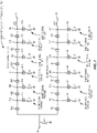
- FIG. 3 is a schematic illustrating RF filtering circuitry 24 according to one embodiment of the present disclosure.
- the RF filtering circuitry 24 includes a first node 26, a second node 28, a series signal path 30 between the first node 26 and the second node 28, and a number of shunt signal paths 32 between the series signal path 30 and a ground.
- a first acoustic resonator R1 is coupled between the first node 26 and a first intermediate node 34A.
- a second acoustic resonator R2 and a first inductor L1 are coupled in series between the first intermediate node 34A and ground to provide a first shunt signal path 32A.
- a third acoustic resonator R3 is coupled between the first intermediate node 34A and a second intermediate node 34B.
- a fourth acoustic resonator R4 and a second inductor L2 are coupled in series between the second intermediate node 34B and ground to provide a second shunt signal path 32B.
- a fifth acoustic resonator R5 is coupled between the second intermediate node 34B and a third intermediate node 34C.
- a sixth acoustic resonator R6 and a third inductor L3 are coupled between the third intermediate node 34C and ground to provide a third shunt signal path 32C.
- a seventh acoustic resonator R7 is coupled between the third intermediate node 34C and a fourth intermediate node 34D.
- An eighth acoustic resonator R8 and a fourth inductor L4 are coupled in series between the fourth intermediate node 34D and ground to provide a fourth shunt signal path 32D.
- a ninth acoustic resonator R9 is coupled between the fourth intermediate node 34D and a fifth intermediate node 34E.
- a tenth acoustic resonator R10 and a fifth inductor L5 are coupled in series between the fifth intermediate node 34E and ground to provide a fifth shunt signal path 32E.
- An eleventh acoustic resonator R11 is coupled between the fifth intermediate node 34E and the second node 28.
- a twelfth acoustic resonator R12, and a sixth inductor L6 are coupled in series between the second node 28 and ground to provide a sixth shunt signal path 32F.
- RF filtering circuitry 24 shown in Figure 3 is merely exemplary.
- the number of acoustic resonators and inductors as well as their placement between the first node 26, the second node 28, and ground will vary based on the particular specifications for the RF filtering circuitry 24.
- the concepts described in the present disclosure apply equally to all topologies of RF filtering circuitry, including ladder topologies, lattice topologies, transversal topologies, or any other type of topology.
- the acoustic resonators (R1-R12) in the RF filtering circuitry 24 are uniform with respect to their performance characteristics such as electromechanical coupling (and thus bandwidth) and quality factor. This is because all of the acoustic resonators (R1-R12) utilize the same material for the piezoelectric layer 20 thereof. For example, all of the acoustic resonators (R1-R12) have a piezoelectric layer 20 that is one of intrinsic aluminum nitride or aluminum nitride doped with scandium. Due to the trade-off between quality factor and electromechanical coupling discussed above with respect to these materials, this results in sub-optimal performance of the RF filtering circuitry 24 either with respect to electromechanical coupling (and thus bandwidth) or quality factor.
- the acoustic resonators (R1-R12) having a first electromechanical coupling coefficient and a first quality factor and provide the remaining acoustic resonators (R1-R12) having a second electromechanical coupling coefficient and a second quality factor.
- the first electromechanical coupling coefficient is different from the second coupling coefficient
- the first quality factor is different from the second quality factor.
- the first electromechanical coupling coefficient may be less than the second electromechanical coupling coefficient and the first quality factor may be greater than the second quality factor.
- One way to achieve the hybrid approach is by providing the piezoelectric layer 20 of some of the acoustic resonators (R1-R12) comprising a first piezoelectric material (which provides the first quality factor and the first electromechanical coupling coefficient) and providing the piezoelectric layer 20 of the remaining ones of the acoustic resonators (R1-R12) comprising a second piezoelectric material (which provides the second quality factor and the second electromechanical coupling coefficient) that is different than the first piezoelectric material.
- the second acoustic resonator R2 and the twelfth acoustic resonator R12 may have a piezoelectric layer 20 comprising a first piezoelectric material, while the remaining acoustic resonators (R1 and R3-R11) have a piezoelectric layer 20 comprising a second piezoelectric material.
- the first piezoelectric material is intrinsic aluminum nitride and the second piezoelectric material is aluminum nitride doped with scandium.
- first piezoelectric material is aluminum nitride doped with scandium and the second piezoelectric material is intrinsic aluminum nitride.
- first piezoelectric material is aluminum nitride doped with scandium at a first concentration and the second piezoelectric material is aluminum nitride doped with scandium at a second doping concentration that is greater than the first doping concentration.
- the second doping concentration is at least 1% greater than the first doping concentration.
- present disclosure also contemplates embodiments in which the second doping concentration is more than 1% greater than the first doping concentration.
- the second doping concentration may be at least 2% greater than the first doping concentration, at least 3% greater, at least 4% greater, at least 5% greater, etc.
- the present disclosure is not limited to aluminum nitride for the first piezoelectric material and the second piezoelectric material.
- the first piezoelectric material and the second piezoelectric material may be any combination of lithium tantalate, zinc oxide, and lead zirconate titanate.
- the present disclosure is not limited to scandium as a dopant.
- the dopant may be any combination of gallium, yttrium, chromium, or co-doping of multiple elements such as magnesium and zirconium and magnesium and titanium.
- any ones of the acoustic resonators (R1-R12) may have a piezoelectric layer 20 comprising a different piezoelectric material than any other ones of the acoustic resonators (R1-R12).
- the ones of the acoustic resonators (R1-R12) having a piezoelectric layer 20 comprising the first piezoelectric material are provided in one or more of the shunt signal paths 32. In other embodiments, the ones of the acoustic resonators (R1-R12) having a piezoelectric layer 20 comprising the first piezoelectric material are provided in the series signal path 30. In still other embodiments, the ones of the acoustic resonators (R1-R25) having a piezoelectric layer 20 comprising the first piezoelectric material are provided in both the series signal path 30 and one or more of the shunt signal paths 32.
- those skilled in the art may use a piezoelectric layer 20 with a material providing higher electromechanical coupling in the acoustic resonators (R1-R12) responsible for providing the passband of the filter response of the RF filtering circuitry 24 while using a piezoelectric layer 20 with a material providing a higher quality factor in the acoustic resonators (R1-R12) responsible for providing the edges of the filter response of the RF filtering circuitry 24.
- the acoustic resonators (R1-R12) of the RF filtering circuitry 24 would be provided having a uniform piezoelectric layer 20. Accordingly, the acoustic resonators (R1-R12) of the RF filtering circuitry 24 would generally be provided on a single acoustic die. In some embodiments, all of the acoustic resonators (R1-R12) in the RF filtering circuitry 24 are similarly provided on the same acoustic die. Such an approach may require more advanced die fabrication techniques due to differences in the material and/or doping of the piezoelectric layer 20 of the acoustic resonators (R1 -R12).
- the acoustic resonators (R1-R12) may be provided on separate die based on the material used for the piezoelectric layer 20 thereof.
- a first acoustic die may be used for the ones of the acoustic resonators (R1-R12) having a piezoelectric layer 20 comprising the first piezoelectric material while a second acoustic die may be used for the ones of the acoustic resonators (R1-R12) having a piezoelectric layer 20 comprising the second piezoelectric material.
- a first subset of acoustic resonators having a piezoelectric layer 20 comprising a first piezoelectric material and a second subset of acoustic resonators having a piezoelectric layer 20 comprising a second piezoelectric material contemplates a first subset of acoustic resonators having a piezoelectric layer 20 comprising a first piezoelectric material and a second subset of acoustic resonators having a piezoelectric layer 20 comprising a second piezoelectric material
- the present disclosure also applies to RF filtering circuitry in which the acoustic resonators therein are divided into any number of subsets, each having a different piezoelectric material.
- the present disclosure applies to RF filtering circuitry having a first subset of acoustic resonators wherein the piezoelectric layer 20 is intrinsic aluminum nitride, a second subset of acoustic resonators wherein the piezoelectric layer 20 thereof is aluminum nitride doped with scandium at a first doping concentration, and a third subset of acoustic resonators wherein the piezoelectric layer 20 thereof is aluminum nitride doped with scandium at a second doping concentration that is greater than the first doping concentration.
- Those skilled in the art will recognize that the present disclosure generally contemplates the use of different piezoelectric materials for different subsets of acoustic resonators in RF filtering circuitry in order to improve the performance thereof.
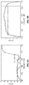
- Figures 4A and 4B are graphs illustrating the input impedance and quality factor of an acoustic resonator having an intrinsically doped piezoelectric layer (e.g., aluminum nitride) and a doped piezoelectric layer (e.g., aluminum nitride doped with scandium), respectively.
- a solid line in the graphs shown in Figures 4A and 4B illustrates input impedance
- a dashed line illustrates a Bode plot of quality factor.
- the distance between the resonance and anti-resonance frequencies of the acoustic resonator with an intrinsically doped piezoelectric layer is relatively small when compared with the acoustic resonator having a doped piezoelectric layer.
- the graphs also show a significantly higher quality factor for the acoustic resonator with the intrinsic piezoelectric layer, thus illustrating the tradeoff between electromechanical coupling (and thus bandwidth) and quality factor discussed above.
- Figures 5A and 5B are graphs illustrating the input impedance and S parameter (
- a doped piezoelectric layer e.g., aluminum nitride doped with scandium
- the solid line illustrates
- the dashed line illustrates the input impedance of a first one of the pair of acoustic resonators
- the dotted and dashed line illustrates the input impedance of a second one of the pair of acoustic resonators
- the first one of the pair of acoustic resonators includes an intrinsic piezoelectric layer while the second one of the pair of acoustic resonators includes a doped piezoelectric layer.
- Figure 5B shows greater steepness and thus lower loss at the lower band edge.
- Figure 6A is a graph illustrating the rejection of the RF filtering circuitry 24 around the Industrial, Scientific, and Medical (ISM) band.
- the dashed line represents the performance of the RF filtering circuitry 24 if all of the acoustic resonators therein have a piezoelectric layer comprised of the same material (e.g., intrinsic aluminum nitride), and the solid line represents the performance of the RF filtering circuitry 24 wherein some of the acoustic resonators have a piezoelectric layer comprising a material that is different than the remaining acoustic resonators (e.g., intrinsic aluminum nitride and aluminum nitride doped with scandium) as discussed above.
- the remaining acoustic resonators e.g., intrinsic aluminum nitride and aluminum nitride doped with scandium
- the hatched boxes in the graph illustrate a desired rejection for the ISM band.
- the steepness and thus rejection of the ISM band is improved when using a hybrid approach wherein some of the acoustic resonators have a piezoelectric layer that comprises a different material than the others in order to provide high electromechanical coupling in some of the acoustic resonators and high quality factor in other ones of the acoustic resonators.
- Figure 6B is a graph illustrating the insertion loss of the RF filtering circuitry 24 within a band of interest.
- the dashed line represents the performance of the RF filtering circuitry 24 if all of the acoustic resonators therein have a piezoelectric layer comprised of the same material (e.g., intrinsic aluminum nitride), and the solid line represents the performance of the RF filtering circuitry 24 wherein some of the acoustic resonators have a piezoelectric material that is different than the remaining acoustic resonators (e.g., intrinsic aluminum nitride and aluminum nitride doped with scandium) as discussed above.
- the remaining acoustic resonators e.g., intrinsic aluminum nitride and aluminum nitride doped with scandium
- the hatched boxes in the graph illustrate the band of interest.
- the hybrid approach wherein some of the acoustic resonators have a piezoelectric material that is different than the others results in higher bandwidth and thus less loss at the bottom end of the band of interest.
- the graphs in Figures 5A, 5B , 6A, and 6B illustrate that using a hybrid approach wherein a subset of the acoustic resonators has a piezoelectric layer with a different material than the rest of the acoustic resonators such as the one discussed above results in a better tradeoff between electromechanical coupling (and thus bandwidth) and quality factor than an approach in which all of the acoustic resonators in RF filtering circuitry have a uniform piezoelectric layer and thus the same relationship between electromechanical coupling, bandwidth, and quality factor.
- the RF filtering circuitry 24 shown in Figure 3 is merely exemplary.
- the principles of the present disclosure can be applied to any topology of RF filtering circuitry, including single band filters, diplexers, triplexers, and the like.
- Figure 7 thus shows the RF filtering circuitry 24 configured as a diplexer.
- the RF filtering circuitry 24 includes the first node 26, the second node 28, the series signal path 30 between the first node 26 and the second node 28, and the number of shunt signal paths 32 between the series signal path 30 and a ground.
- the configuration of the series signal path 30 and the shunt signal paths 32 coupled thereto is similar to that shown in Figure 2 .
- a first input output inductor LIO1 is coupled between the first node 26 and ground.
- the first acoustic resonator R1 is coupled between the first node 26 and the first intermediate node 34A.
- the second acoustic resonator R2 and the first inductor L1 are coupled in series between the first intermediate node 34A and ground to provide the first shunt signal path 32A.
- the third acoustic resonator R3 is coupled between the first intermediate node 34A and the second intermediate node 34B.
- the fourth acoustic resonator R4 and the second inductor L2 are coupled in series between the second intermediate node 34B and ground to provide the second shunt signal path 32B.
- the fifth acoustic resonator R5 is coupled between the second intermediate node 34B and the third intermediate node 34C.
- the sixth acoustic resonator R6 and the third inductor L3 are coupled between the third intermediate node 34C and ground to provide the third shunt signal path 32C.
- the seventh acoustic resonator R7 is coupled between the third intermediate node 34C and the fourth intermediate node 34D.
- the eighth acoustic resonator R8 and the fourth inductor L4 are coupled in series between the fourth intermediate node 34D and ground to provide the fourth shunt signal path 32D.
- the ninth acoustic resonator R9 is coupled between the fourth intermediate node 34D and the fifth intermediate node 34E.
- the tenth acoustic resonator R10 and the fifth inductor L5 are coupled in series between the fifth intermediate node 34E and ground to provide the fifth shunt signal path 32E.
- the eleventh acoustic resonator R11 is coupled between the fifth intermediate node 34E and a sixth intermediate node 34F.
- the twelfth acoustic resonator R12 and the sixth inductor L6 are coupled in series between the sixth intermediate node 34F and ground to provide the sixth shunt signal path 32F.
- a second input output inductor LIO2 is coupled between the sixth intermediate node 34F and the second node 28.
- the RF filtering circuitry 24 further includes a third node 38, an additional series signal path 40 coupled between the first node 26 and the third node 38, and a number of additional shunt signal paths 42 coupled between the additional series signal path 40 and a ground.
- a thirteenth acoustic resonator R13 is coupled between the first node 26 and a seventh intermediate node 34G.
- a fourteenth acoustic resonator R14 and a seventh inductor L7 are coupled in series between the seventh intermediate node 34G and ground to provide a first additional shunt signal path 42A.
- a fifteenth acoustic resonator R15 is coupled between the seventh intermediate node 34G and an eighth intermediate node 34H.
- a sixteenth acoustic resonator R16 and an eighth inductor L8 are coupled in series between the eighth intermediate node 34H and ground to provide a second additional shunt signal path 42B.
- a seventeenth acoustic resonator R17 is coupled between the eighth intermediate node 34H and a ninth intermediate node 34I.
- An eighteenth acoustic resonator R18 and a ninth inductor L9 are coupled in series between the ninth intermediate node 34I and ground to provide a third additional shunt signal path 42C.
- a nineteenth acoustic resonator R19 is coupled between the ninth intermediate node 34I and a tenth intermediate node 34J.
- a twentieth acoustic resonator R20 and a tenth inductor L10 are coupled in series between the tenth intermediate node 34J and ground to provide a fourth additional shunt signal path 42D.
- a twenty-first acoustic resonator R21 is coupled between the tenth intermediate node 34J and an eleventh intermediate node 34K.
- a twenty-second acoustic resonator R22 and an eleventh inductor L11 are coupled in series between the eleventh intermediate node 34K and ground to provide a fifth additional shunt signal path 42E.
- a twenty-third acoustic resonator R23 is coupled between the eleventh intermediate node 34K and a twelfth intermediate node 34L.
- a twenty-fourth acoustic resonator R24 is coupled in series with a twelfth inductor L12 between the twelfth intermediate node 34L and ground to provide a sixth additional shunt signal path 42F.
- a third input output inductor LIO3 is coupled between the twelfth intermediate node 34L and the third node 38.
- RF filtering circuitry 24 shown in Figure 7 is merely exemplary.
- the number of acoustic resonators as well as their placement between the first node 26, the second node 28, the third node 38, and ground will vary based on the particular specifications for the RF filtering circuitry 24.
- the concepts described in the present disclosure apply equally to all topologies of RF filtering circuitry, including lattice and modified lattice topologies.
- the RF filtering circuitry 24 shown in Figure 7 may provide diplexer functionality such that signals within a first RF band are isolated and passed between the first node 26 and the second node 28 and RF signals within a second RF band are isolated and passed between the first node 26 and the third node 38.
- Using a hybrid approach as discussed above may involve providing the second acoustic resonator R2, the twelfth acoustic resonator R12, the thirteenth acoustic resonator R13, the fifteenth acoustic resonator R15, the twenty-first acoustic resonator R21, and the twenty-third acoustic resonator R23 with a piezoelectric layer 20 comprising a first piezoelectric material and providing the remaining ones of the acoustic resonators (R1, R3-R11, R14, R16-R20, R22, and R24) with a piezoelectric layer 20 comprising a second piezoelectric material that is different than the first piezoelectric material.
- the first piezoelectric material is intrinsic aluminum nitride and the second piezoelectric material is aluminum nitride doped with scandium.
- the first piezoelectric material is aluminum nitride doped with scandium at a first concentration and the second piezoelectric material is aluminum nitride doped with scandium at a second doping concentration that is greater than the first doping concentration.
- the second doping concentration is 1% greater than the first doping concentration.
- the present disclosure also contemplates embodiments in which the second doping concentration is more than 1% greater than the first doping concentration.
- the second doping concentration may be at least 2% greater than the first doping concentration, at least 3% greater, at least 4% greater, at least 5% greater, etc.
- any ones of the acoustic resonators (R1-R24) may have a piezoelectric layer 20 comprising a different material than any other ones of the acoustic resonators (R1-R24).
- those skilled in the art may use a piezoelectric layer 20 with a material providing higher electromechanical coupling in the acoustic resonators (R1-R24) responsible for providing the passband of the filter response while using a piezoelectric layer 20 with a material providing a higher quality factor in the acoustic resonators (R1-R24) responsible for providing the edges of the filter response of the RF filtering circuitry 24.
- the acoustic resonators (R1-R24) of the RF filtering circuitry 24 would be provided having a piezoelectric layer 20 that is uniform. Accordingly, the acoustic resonators (R1-R24) of the RF filtering circuitry 24 would generally be provided on a single acoustic die. In some embodiments, all of the acoustic resonators (R1-R24) are similarly provided on the same acoustic die. Such an approach may require more advanced die fabrication techniques due to differences in the material and/or doping in the piezoelectric layer 20 of the acoustic resonators (R1-R24).
- the acoustic resonators (R1-R24) may be separated into separate die based on the material used for the piezoelectric layer 20 thereof.
- a first acoustic die may be used for the ones of the acoustic resonators (R1-R24) having a piezoelectric layer 20 comprising the first piezoelectric material while a second acoustic die may be used for the ones of the acoustic resonators (R1-R24) having a piezoelectric layer 20 comprising the second piezoelectric material.
- a first subset of acoustic resonators having a piezoelectric layer 20 comprising a first piezoelectric material and a second subset of acoustic resonators having a piezoelectric layer 20 comprising a second piezoelectric material contemplates a first subset of acoustic resonators having a piezoelectric layer 20 comprising a first piezoelectric material and a second subset of acoustic resonators having a piezoelectric layer 20 comprising a second piezoelectric material
- the present disclosure also applies to RF filtering circuitry in which the acoustic resonators therein are divided into any number of subsets, each having a different piezoelectric material.
- the present disclosure applies to RF filtering circuitry having a first subset of acoustic resonators wherein the piezoelectric layer 20 is intrinsic aluminum nitride, a second subset of acoustic resonators wherein the piezoelectric layer 20 thereof is aluminum nitride doped with scandium at a first doping concentration, and a third subset of acoustic resonators wherein the piezoelectric layer 20 thereof is aluminum nitride doped with scandium at a second doping concentration that is greater than the first doping concentration.
- Those skilled in the art will recognize that the present disclosure generally contemplates the use of different piezoelectric materials for different subsets of acoustic resonators in RF filtering circuitry in order to improve the performance thereof.
Landscapes
- Physics & Mathematics (AREA)
- Acoustics & Sound (AREA)
- Chemical & Material Sciences (AREA)
- Crystallography & Structural Chemistry (AREA)
- Engineering & Computer Science (AREA)
- Ceramic Engineering (AREA)
- Piezo-Electric Or Mechanical Vibrators, Or Delay Or Filter Circuits (AREA)
- Surface Acoustic Wave Elements And Circuit Networks Thereof (AREA)
- Diaphragms For Electromechanical Transducers (AREA)
- Filters And Equalizers (AREA)
- Control Of Motors That Do Not Use Commutators (AREA)
Applications Claiming Priority (1)
| Application Number | Priority Date | Filing Date | Title |
|---|---|---|---|
| US17/152,110 US11575363B2 (en) | 2021-01-19 | 2021-01-19 | Hybrid bulk acoustic wave filter |
Publications (1)
| Publication Number | Publication Date |
|---|---|
| EP4030620A1 true EP4030620A1 (en) | 2022-07-20 |
Family
ID=79231111
Family Applications (1)
| Application Number | Title | Priority Date | Filing Date |
|---|---|---|---|
| EP22150239.6A Pending EP4030620A1 (en) | 2021-01-19 | 2022-01-04 | Hybrid bulk acoustic wave filter |
Country Status (5)
| Country | Link |
|---|---|
| US (1) | US11575363B2 (enExample) |
| EP (1) | EP4030620A1 (enExample) |
| JP (1) | JP2022111108A (enExample) |
| KR (1) | KR20220105131A (enExample) |
| TW (1) | TW202243400A (enExample) |
Families Citing this family (1)
| Publication number | Priority date | Publication date | Assignee | Title |
|---|---|---|---|---|
| US12445109B2 (en) * | 2019-07-31 | 2025-10-14 | QXONIX Inc. | Structures, acoustic wave resonators, layers, devices and systems |
Citations (4)
| Publication number | Priority date | Publication date | Assignee | Title |
|---|---|---|---|---|
| US20040263286A1 (en) * | 2001-07-18 | 2004-12-30 | Michael Unterberger | Reactance filter having an improved edge steepness |
| US20140125203A1 (en) * | 2009-11-25 | 2014-05-08 | Avago Technologies General Ip (Singapore) Pte. Ltd. | Bulk acoustic wave (baw) resonator structure having an electrode with a cantilevered portion and a piezoelectric layer with varying amounts of dopant |
| US20170310302A1 (en) * | 2016-04-25 | 2017-10-26 | Infineon Technologies Ag | Tunable Resonator Element, Filter Circuit and Method |
| CN111917392A (zh) * | 2020-04-14 | 2020-11-10 | 诺思(天津)微系统有限责任公司 | 压电滤波器及其带外抑制改善方法、多工器、通信设备 |
Family Cites Families (131)
| Publication number | Priority date | Publication date | Assignee | Title |
|---|---|---|---|---|
| US3731230A (en) | 1971-12-17 | 1973-05-01 | Motorola Inc | Broadband circuit for minimizing the effects of crystal shunt capacitance |
| US3875533A (en) | 1973-10-15 | 1975-04-01 | Motorola Inc | Crystal controlled overtone oscillator having a rejection circuit for preventing oscillation at undesired overtones |
| DK147560C (da) | 1980-03-13 | 1985-07-22 | Bang & Olufsen As | Modtagerantenne for magnetiske signaler, f.eks. ferritantenne |
| US4577168A (en) | 1984-12-03 | 1986-03-18 | R. F. Monolithics, Inc. | Notch filter |
| US5291159A (en) | 1992-07-20 | 1994-03-01 | Westinghouse Electric Corp. | Acoustic resonator filter with electrically variable center frequency and bandwidth |
| US5821833A (en) | 1995-12-26 | 1998-10-13 | Tfr Technologies, Inc. | Stacked crystal filter device and method of making |
| US6246153B1 (en) | 1998-07-16 | 2001-06-12 | Face International Corp. | Positive feedback resonant transducer circuit |
| US6067391A (en) | 1998-09-02 | 2000-05-23 | The United States Of America As Represented By The Secretary Of The Air Force | Multiply periodic refractive index modulated optical filters |
| KR100301854B1 (ko) | 1999-06-02 | 2001-09-29 | 구본준, 론 위라하디락사 | 투과 및 반사형 겸용 액정표시장치 |
| US6496085B2 (en) | 2001-01-02 | 2002-12-17 | Nokia Mobile Phones Ltd | Solidly mounted multi-resonator bulk acoustic wave filter with a patterned acoustic mirror |
| TW488044B (en) | 2001-02-09 | 2002-05-21 | Asia Pacific Microsystems Inc | Bulk acoustic filter and its package |
| JP3973915B2 (ja) | 2001-03-30 | 2007-09-12 | 株式会社日立メディアエレクトロニクス | 高周波フィルタ、高周波回路、アンテナ共用器及び無線端末 |
| JP4256682B2 (ja) | 2001-04-25 | 2009-04-22 | エヌエックスピー ビー ヴィ | 2つのピエゾ電気層を持つ装置 |
| DE10149542A1 (de) | 2001-10-08 | 2003-04-17 | Infineon Technologies Ag | BAW-Resonator |
| US6720844B1 (en) | 2001-11-16 | 2004-04-13 | Tfr Technologies, Inc. | Coupled resonator bulk acoustic wave filter |
| US6670866B2 (en) | 2002-01-09 | 2003-12-30 | Nokia Corporation | Bulk acoustic wave resonator with two piezoelectric layers as balun in filters and duplexers |
| DE10225202B4 (de) | 2002-06-06 | 2017-06-01 | Epcos Ag | Mit akustischen Wellen arbeitendes Bauelement mit einem Anpassnetzwerk |
| JP3963824B2 (ja) | 2002-11-22 | 2007-08-22 | 富士通メディアデバイス株式会社 | フィルタ素子、それを有するフィルタ装置、分波器及び高周波回路 |
| JP2004304490A (ja) | 2003-03-31 | 2004-10-28 | Tdk Corp | 薄膜圧電共振子の製造方法、薄膜圧電共振子の製造装置、薄膜圧電共振子および電子部品 |
| DE10319554B4 (de) | 2003-04-30 | 2018-05-09 | Snaptrack, Inc. | Mit akustischen Volumenwellen arbeitendes Bauelement mit gekoppelten Resonatoren |
| US6927651B2 (en) | 2003-05-12 | 2005-08-09 | Agilent Technologies, Inc. | Acoustic resonator devices having multiple resonant frequencies and methods of making the same |
| JP4229122B2 (ja) | 2003-05-26 | 2009-02-25 | 株式会社村田製作所 | 圧電電子部品、およびその製造方法、通信機 |
| JP2005117641A (ja) | 2003-09-17 | 2005-04-28 | Matsushita Electric Ind Co Ltd | 圧電体共振器、それを用いたフィルタ及び共用器 |
| US7391285B2 (en) | 2003-10-30 | 2008-06-24 | Avago Technologies Wireless Ip Pte Ltd | Film acoustically-coupled transformer |
| EP1528677B1 (en) | 2003-10-30 | 2006-05-10 | Agilent Technologies, Inc. | Film acoustically-coupled transformer with two reverse c-axis piezoelectric elements |
| US6946928B2 (en) | 2003-10-30 | 2005-09-20 | Agilent Technologies, Inc. | Thin-film acoustically-coupled transformer |
| JP3950445B2 (ja) | 2003-11-05 | 2007-08-01 | Tdk株式会社 | デュプレクサ |
| JP3944161B2 (ja) | 2003-12-25 | 2007-07-11 | 株式会社東芝 | 薄膜バルク波音響共振器及び薄膜バルク波音響共振器の製造方法 |
| US6963257B2 (en) | 2004-03-19 | 2005-11-08 | Nokia Corporation | Coupled BAW resonator based duplexers |
| DE102004032930A1 (de) | 2004-07-07 | 2006-02-02 | Epcos Ag | Beidseitig symmetrisch betreibbares Filter mit Volumenwellenresonatoren |
| DE102004049499B4 (de) | 2004-10-11 | 2017-12-21 | Snaptrack, Inc. | Mit akustischen Volumenwellen arbeitende Schaltung und Bauelement mit der Schaltung |
| US7098758B2 (en) | 2004-11-03 | 2006-08-29 | Avago Technologies Wireless Ip (Singapore) Pte. Ltd. | Acoustically coupled thin-film resonators having an electrode with a tapered edge |
| US7333831B2 (en) | 2005-02-07 | 2008-02-19 | Nxp B.V. | Interchangeable receive inputs for band and system swappability in communication systems and related methods |
| US7436269B2 (en) | 2005-04-18 | 2008-10-14 | Avago Technologies Wireless Ip (Singapore) Pte. Ltd. | Acoustically coupled resonators and method of making the same |
| US7535323B2 (en) | 2006-07-10 | 2009-05-19 | Skyworks Solutions, Inc. | Bulk acoustic wave filter with reduced nonlinear signal distortion |
| US7515018B2 (en) | 2006-08-31 | 2009-04-07 | Martin Handtmann | Acoustic resonator |
| JP5036435B2 (ja) | 2006-09-01 | 2012-09-26 | 太陽誘電株式会社 | 弾性波デバイス、フィルタおよび分波器 |
| JP2008172711A (ja) | 2007-01-15 | 2008-07-24 | Hitachi Media Electoronics Co Ltd | 薄膜バルク弾性波共振器およびフィルタおよびそれを用いた高周波モジュール |
| US7804374B1 (en) | 2007-02-15 | 2010-09-28 | Discera, Inc. | Feedthrough capacitance compensation for resonant devices |
| US7825749B2 (en) | 2007-05-31 | 2010-11-02 | Avago Technologies Wireless Ip (Singapore) Pte. Ltd. | Integrated coupled resonator filter and bulk acoustic wave devices |
| US7786825B2 (en) | 2007-05-31 | 2010-08-31 | Avago Technologies Wireless Ip (Singapore) Pte. Ltd. | Bulk acoustic wave device with coupled resonators |
| US7898493B1 (en) | 2007-06-13 | 2011-03-01 | The Ohio State University | Implementation of ultra wide band (UWB) electrically small antennas by means of distributed non foster loading |
| US8018303B2 (en) | 2007-10-12 | 2011-09-13 | Avago Technologies Wireless Ip (Singapore) Pte. Ltd. | Bulk acoustic wave device |
| US7786826B2 (en) | 2007-10-12 | 2010-08-31 | Avago Technologies Wireless Ip (Singapore) Pte. Ltd. | Apparatus with acoustically coupled BAW resonators and a method for matching impedances |
| FR2926417B1 (fr) | 2008-01-15 | 2010-01-08 | Commissariat Energie Atomique | Filtre d'amplification de puissance de signaux radiofrequence |
| JP5441095B2 (ja) | 2008-01-31 | 2014-03-12 | 太陽誘電株式会社 | 弾性波デバイス、デュープレクサ、通信モジュール、および通信装置 |
| US7855618B2 (en) | 2008-04-30 | 2010-12-21 | Avago Technologies Wireless Ip (Singapore) Pte. Ltd. | Bulk acoustic resonator electrical impedance transformers |
| US7889024B2 (en) | 2008-08-29 | 2011-02-15 | Avago Technologies Wireless Ip (Singapore) Pte. Ltd. | Single cavity acoustic resonators and electrical filters comprising single cavity acoustic resonators |
| CN102273071A (zh) | 2009-01-07 | 2011-12-07 | 株式会社大真空 | 压电振动设备的制造方法 |
| US8373519B2 (en) | 2009-01-26 | 2013-02-12 | Resonance Semiconductor Corporation | Switchable power combiner |
| US8248185B2 (en) | 2009-06-24 | 2012-08-21 | Avago Technologies Wireless Ip (Singapore) Pte. Ltd. | Acoustic resonator structure comprising a bridge |
| JP5419617B2 (ja) | 2009-09-28 | 2014-02-19 | 太陽誘電株式会社 | フィルタ、通信モジュール、および通信装置 |
| JP5392353B2 (ja) | 2009-10-19 | 2014-01-22 | 株式会社村田製作所 | 弾性表面波装置 |
| JP2011109306A (ja) | 2009-11-16 | 2011-06-02 | Murata Mfg Co Ltd | 弾性表面波素子 |
| US9847768B2 (en) | 2009-11-23 | 2017-12-19 | Avago Technologies General Ip (Singapore) Pte. Ltd. | Polarity determining seed layer and method of fabricating piezoelectric materials with specific C-axis |
| US9679765B2 (en) | 2010-01-22 | 2017-06-13 | Avago Technologies General Ip (Singapore) Pte. Ltd. | Method of fabricating rare-earth doped piezoelectric material with various amounts of dopants and a selected C-axis orientation |
| US9243316B2 (en) | 2010-01-22 | 2016-01-26 | Avago Technologies General Ip (Singapore) Pte. Ltd. | Method of fabricating piezoelectric material with selected c-axis orientation |
| US8768267B2 (en) | 2010-02-03 | 2014-07-01 | Hollinworth Fund, L.L.C. | Switchless band separation for transceivers |
| US8576024B2 (en) | 2010-02-11 | 2013-11-05 | Hollinworth Fund, L.L.C. | Electro-acoustic filter |
| US8508315B2 (en) | 2010-02-23 | 2013-08-13 | Avago Technologies General Ip (Singapore) Pte. Ltd. | Acoustically coupled resonator filter with impedance transformation ratio controlled by resonant frequency difference between two coupled resonators |
| JP5519326B2 (ja) | 2010-02-25 | 2014-06-11 | 太陽誘電株式会社 | フィルタ、デュープレクサ、通信モジュール、通信装置 |
| AT509633A1 (de) | 2010-03-29 | 2011-10-15 | Ctr Carinthian Tech Res Ag | Hochtemperaturbeständige, elektrisch leitfähige dünnschichten |
| JP5187597B2 (ja) | 2010-07-05 | 2013-04-24 | 株式会社村田製作所 | 弾性波素子 |
| US8674789B2 (en) | 2010-07-07 | 2014-03-18 | Wei Pang | Serially connected first and second coupled resonator filters configured to provide at least one feedback capacitor |
| US8575820B2 (en) | 2011-03-29 | 2013-11-05 | Avago Technologies General Ip (Singapore) Pte. Ltd. | Stacked bulk acoustic resonator |
| JP2012257050A (ja) | 2011-06-08 | 2012-12-27 | Nippon Dempa Kogyo Co Ltd | ハイパス型のノッチフィルタ及びこのフィルタを備えた電子機器 |
| USRE47991E1 (en) | 2011-06-28 | 2020-05-12 | Kyocera Corporation | Acoustic wave element and acoustic wave device using same |
| WO2013031617A1 (ja) | 2011-08-26 | 2013-03-07 | 株式会社村田製作所 | 圧電デバイス、および、圧電デバイスの製造方法 |
| US8923794B2 (en) | 2011-11-02 | 2014-12-30 | Triquint Semiconductor, Inc. | Temperature compensation of acoustic resonators in the electrical domain |
| JP6017868B2 (ja) | 2011-11-04 | 2016-11-02 | 太陽誘電株式会社 | 分波器、フィルタ及び通信モジュール |
| US9054671B2 (en) | 2011-11-09 | 2015-06-09 | International Business Machines Corporation | Tunable filter structures and design structures |
| JP6116120B2 (ja) | 2012-01-24 | 2017-04-19 | 太陽誘電株式会社 | 弾性波デバイス及び弾性波デバイスの製造方法 |
| US9065421B2 (en) | 2012-01-31 | 2015-06-23 | Avago Technologies General Ip (Singapore) Pte. Ltd. | Film bulk acoustic resonator with multi-layers of different piezoelectric materials and method of making |
| US8981627B2 (en) | 2012-06-04 | 2015-03-17 | Tdk Corporation | Piezoelectric device with electrode films and electroconductive oxide film |
| FR2996061B1 (fr) | 2012-09-27 | 2015-12-25 | Commissariat Energie Atomique | Structure acoustique comportant au moins un resonateur et au moins une capacite cointegree dans une meme couche piezoelectrique ou ferroelectrique |
| EP2913923A4 (en) | 2012-10-24 | 2016-06-01 | Murata Manufacturing Co | FILTER DEVICE |
| WO2014094887A1 (en) * | 2012-12-21 | 2014-06-26 | Epcos Ag | Mems component comprising aln and sc and method for manufacturing a mems component |
| DE112012007237T5 (de) * | 2012-12-21 | 2015-10-15 | Epcos Ag | BAW-Bauelement, Schichtsystem für ein BAW-Bauelement und Verfahren zur Herstellung eines BAW-Bauelements |
| US9512796B2 (en) | 2013-02-08 | 2016-12-06 | Toyota Jidosha Kabushiki Kaisha | Exhaust purification apparatus for internal combustion engine |
| CN105122645B (zh) | 2013-04-11 | 2018-02-13 | 株式会社村田制作所 | 高频模块 |
| JP6098715B2 (ja) | 2013-05-14 | 2017-03-22 | 株式会社村田製作所 | 弾性波装置およびその製造方法 |
| JP6315650B2 (ja) * | 2013-07-31 | 2018-04-25 | 太陽誘電株式会社 | 電子デバイス |
| US9437802B2 (en) | 2013-08-21 | 2016-09-06 | Fujifilm Dimatix, Inc. | Multi-layered thin film piezoelectric devices and methods of making the same |
| WO2015119176A1 (ja) | 2014-02-10 | 2015-08-13 | 株式会社村田製作所 | フィルタ回路および無線通信装置 |
| CN106031034B (zh) | 2014-03-31 | 2018-09-14 | 株式会社村田制作所 | 弹性波装置 |
| US9548438B2 (en) | 2014-03-31 | 2017-01-17 | Avago Technologies General Ip (Singapore) Pte. Ltd. | Acoustic resonator comprising acoustic redistribution layers |
| DE102014111912B4 (de) | 2014-08-20 | 2024-06-13 | Snaptrack, Inc. | HF-Filter |
| JP6508920B2 (ja) | 2014-11-13 | 2019-05-08 | 太陽誘電株式会社 | 弾性波デバイスおよび送受信デバイス |
| US10333494B2 (en) | 2014-12-24 | 2019-06-25 | Qorvo Us, Inc. | Simplified acoustic RF resonator parallel capacitance compensation |
| US9837984B2 (en) | 2014-12-24 | 2017-12-05 | Qorvo Us, Inc. | RF ladder filter with simplified acoustic RF resonator parallel capacitance compensation |
| KR102117471B1 (ko) | 2015-01-12 | 2020-06-01 | 삼성전기주식회사 | 음향 공진기 및 그 제조 방법 |
| US9584076B2 (en) | 2015-03-06 | 2017-02-28 | Qorvo Us, Inc. | Output matching network for differential power amplifier |
| US9837983B2 (en) | 2015-03-13 | 2017-12-05 | Avago Technologies General Ip (Singapore) Pte. Ltd. | Acoustic filter device with combined passband |
| WO2016158953A1 (ja) | 2015-03-30 | 2016-10-06 | 株式会社村田製作所 | 高周波フィルタ、フロントエンド回路、および通信機器 |
| US9929761B2 (en) | 2015-04-17 | 2018-03-27 | Qorvo Us, Inc. | High band TDD antenna swapping method with improved receiver sensitivity |
| US9524881B2 (en) | 2015-04-30 | 2016-12-20 | Texas Instruments Incorporated | Method for fabricating specific termination angles in titanium tungsten layers |
| WO2017002513A1 (ja) | 2015-07-02 | 2017-01-05 | 株式会社村田製作所 | 弾性波装置 |
| US10097161B2 (en) | 2015-09-25 | 2018-10-09 | Qorvo Us, Inc. | Compensation circuit for acoustic resonators |
| US9847769B2 (en) | 2015-09-25 | 2017-12-19 | Qorvo Us, Inc. | Tunable compensation circuit for filter circuitry using acoustic resonators |
| JP6415419B2 (ja) | 2015-12-02 | 2018-10-31 | 太陽誘電株式会社 | 弾性波フィルタ、デュプレクサ、及びモジュール |
| US10243537B2 (en) | 2016-01-12 | 2019-03-26 | Qorvo Us, Inc. | Compensation circuit for use with acoustic resonators to provide a bandstop |
| US10141644B2 (en) | 2016-04-18 | 2018-11-27 | Qorvo Us, Inc. | Acoustic filter for antennas |
| US10581156B2 (en) | 2016-05-04 | 2020-03-03 | Qorvo Us, Inc. | Compensation circuit to mitigate antenna-to-antenna coupling |
| JP2017208629A (ja) | 2016-05-17 | 2017-11-24 | 株式会社村田製作所 | 弾性波装置 |
| US10581403B2 (en) | 2016-07-11 | 2020-03-03 | Qorvo Us, Inc. | Device having a titanium-alloyed surface |
| KR102776288B1 (ko) | 2016-08-08 | 2025-03-07 | 삼성전기주식회사 | 표면 탄성파 필터 장치 및 이의 제조방법 |
| CN109690944B (zh) * | 2016-09-07 | 2023-02-28 | 株式会社村田制作所 | 弹性波滤波器装置以及复合滤波器装置 |
| US11050412B2 (en) | 2016-09-09 | 2021-06-29 | Qorvo Us, Inc. | Acoustic filter using acoustic coupling |
| US10284174B2 (en) | 2016-09-15 | 2019-05-07 | Qorvo Us, Inc. | Acoustic filter employing inductive coupling |
| US10367470B2 (en) | 2016-10-19 | 2019-07-30 | Qorvo Us, Inc. | Wafer-level-packaged BAW devices with surface mount connection structures |
| KR101953219B1 (ko) | 2016-11-24 | 2019-02-28 | 가부시키가이샤 무라타 세이사쿠쇼 | 탄성파 장치, 고주파 프론트 엔드 회로 및 통신 장치 |
| JP6661521B2 (ja) | 2016-12-05 | 2020-03-11 | 太陽誘電株式会社 | フィルタおよびマルチプレクサ |
| US11165412B2 (en) | 2017-01-30 | 2021-11-02 | Qorvo Us, Inc. | Zero-output coupled resonator filter and related radio frequency filter circuit |
| US11165413B2 (en) | 2017-01-30 | 2021-11-02 | Qorvo Us, Inc. | Coupled resonator structure |
| JP6790907B2 (ja) | 2017-02-23 | 2020-11-25 | 株式会社村田製作所 | マルチプレクサ、送信装置および受信装置 |
| US10873318B2 (en) | 2017-06-08 | 2020-12-22 | Qorvo Us, Inc. | Filter circuits having acoustic wave resonators in a transversal configuration |
| GB2578979B (en) * | 2017-07-07 | 2023-01-18 | Skyworks Solutions Inc | Substituted aluminium nitride for improved acoustic wave filters |
| US10361676B2 (en) | 2017-09-29 | 2019-07-23 | Qorvo Us, Inc. | Baw filter structure with internal electrostatic shielding |
| JP6959819B2 (ja) | 2017-10-02 | 2021-11-05 | 株式会社村田製作所 | マルチプレクサ |
| CN110034744B (zh) | 2017-12-07 | 2025-05-13 | 英飞凌科技股份有限公司 | 可调谐谐振元件、滤波器电路和方法 |
| JP2019114986A (ja) | 2017-12-25 | 2019-07-11 | 株式会社村田製作所 | 弾性波装置 |
| US10700662B2 (en) | 2017-12-28 | 2020-06-30 | Taiyo Yuden Co., Ltd. | Acoustic wave device, filter, and multiplexer |
| JP6812998B2 (ja) | 2018-03-19 | 2021-01-13 | 株式会社村田製作所 | 弾性波装置 |
| US11152913B2 (en) | 2018-03-28 | 2021-10-19 | Qorvo Us, Inc. | Bulk acoustic wave (BAW) resonator |
| US11431316B2 (en) | 2018-09-20 | 2022-08-30 | Qorvo Us, Inc. | Acoustic resonator structure |
| US10985731B2 (en) | 2018-09-20 | 2021-04-20 | Qorvo Us, Inc. | Acoustic resonator structure |
| US11563421B2 (en) | 2018-09-21 | 2023-01-24 | Qorvo Us, Inc. | Acoustic structure having tunable parallel resonance frequency |
| US10958244B2 (en) | 2018-10-26 | 2021-03-23 | Qorvo Us, Inc. | Acoustic filter apparatus having configurable parallel resonance frequencies |
| US11146247B2 (en) | 2019-07-25 | 2021-10-12 | Qorvo Us, Inc. | Stacked crystal filter structures |
| CN111010120A (zh) * | 2019-09-20 | 2020-04-14 | 天津大学 | 具有调节层的体声波谐振器、滤波器和电子设备 |
| KR20220028297A (ko) * | 2020-08-28 | 2022-03-08 | 삼성전기주식회사 | 음향 공진기 필터 |
-
2021
- 2021-01-19 US US17/152,110 patent/US11575363B2/en active Active
-
2022
- 2022-01-04 EP EP22150239.6A patent/EP4030620A1/en active Pending
- 2022-01-13 TW TW111101391A patent/TW202243400A/zh unknown
- 2022-01-13 KR KR1020220005116A patent/KR20220105131A/ko active Pending
- 2022-01-19 JP JP2022006133A patent/JP2022111108A/ja active Pending
Patent Citations (4)
| Publication number | Priority date | Publication date | Assignee | Title |
|---|---|---|---|---|
| US20040263286A1 (en) * | 2001-07-18 | 2004-12-30 | Michael Unterberger | Reactance filter having an improved edge steepness |
| US20140125203A1 (en) * | 2009-11-25 | 2014-05-08 | Avago Technologies General Ip (Singapore) Pte. Ltd. | Bulk acoustic wave (baw) resonator structure having an electrode with a cantilevered portion and a piezoelectric layer with varying amounts of dopant |
| US20170310302A1 (en) * | 2016-04-25 | 2017-10-26 | Infineon Technologies Ag | Tunable Resonator Element, Filter Circuit and Method |
| CN111917392A (zh) * | 2020-04-14 | 2020-11-10 | 诺思(天津)微系统有限责任公司 | 压电滤波器及其带外抑制改善方法、多工器、通信设备 |
Non-Patent Citations (1)
| Title |
|---|
| MILENA MOREIRA ET AL: "Aluminum scandium nitride thin-film bulk acoustic resonators for wide band applications", VACUUM, PERGAMON PRESS, GB, vol. 86, no. 1, 29 March 2011 (2011-03-29), pages 23 - 26, XP028100340 * |
Also Published As
| Publication number | Publication date |
|---|---|
| KR20220105131A (ko) | 2022-07-26 |
| JP2022111108A (ja) | 2022-07-29 |
| TW202243400A (zh) | 2022-11-01 |
| US20220231664A1 (en) | 2022-07-21 |
| US11575363B2 (en) | 2023-02-07 |
Similar Documents
| Publication | Publication Date | Title |
|---|---|---|
| US10211799B2 (en) | High-frequency filter | |
| US7515018B2 (en) | Acoustic resonator | |
| US8063717B2 (en) | Duplexer having resonator filters | |
| US9762208B2 (en) | Very wide bandwidth composite bandpass filter with steep roll-off | |
| CN1739237B (zh) | 具有等谐振频率的谐振滤波器结构 | |
| US20040140866A1 (en) | Ladder filter, branching filter, and communication apparatus | |
| US20150381144A1 (en) | Bulk acoustic resonator comprising aluminum scandium nitride | |
| CN109787581A (zh) | 具有带通和高通双重功能的基于体声波谐振器的滤波器 | |
| US10193527B2 (en) | Branching filter | |
| JP2006513662A5 (enExample) | ||
| CN111200419A (zh) | 一种滤波器、双工器、高频前端电路及通信装置 | |
| EP2936680A1 (en) | Mems component comprising aln and sc and method for manufacturing a mems component | |
| CN112073018A (zh) | 滤波器、双工器、多工器以及通信设备 | |
| KR20020029922A (ko) | 사다리형 필터, 무선 주파수 대역 통과 필터, 무선 주파수수신기 및/또는 송신기 장치 | |
| JP4259576B2 (ja) | 分波器及び弾性表面波フィルタ | |
| US11784628B2 (en) | Bi-polar border region in piezoelectric device | |
| US11082030B2 (en) | High-pass filter and multiplexer | |
| WO2021159881A1 (zh) | 调整fbar寄生分量的方法和滤波器、多工器、通信设备 | |
| EP4030620A1 (en) | Hybrid bulk acoustic wave filter | |
| CN115473509A (zh) | 滤波器、多工器和电子设备 | |
| CN116346069B (zh) | 滤波器和电子设备 | |
| WO2021203761A1 (zh) | 滤波器和多工器以及通信设备 | |
| CN116667813A (zh) | 混合体声波滤波器 | |
| US12500566B2 (en) | Filter, radio frequency device and electronic apparatus | |
| CN114567287B (zh) | 多工器 |
Legal Events
| Date | Code | Title | Description |
|---|---|---|---|
| PUAI | Public reference made under article 153(3) epc to a published international application that has entered the european phase |
Free format text: ORIGINAL CODE: 0009012 |
|
| STAA | Information on the status of an ep patent application or granted ep patent |
Free format text: STATUS: THE APPLICATION HAS BEEN PUBLISHED |
|
| AK | Designated contracting states |
Kind code of ref document: A1 Designated state(s): AL AT BE BG CH CY CZ DE DK EE ES FI FR GB GR HR HU IE IS IT LI LT LU LV MC MK MT NL NO PL PT RO RS SE SI SK SM TR |
|
| STAA | Information on the status of an ep patent application or granted ep patent |
Free format text: STATUS: REQUEST FOR EXAMINATION WAS MADE |
|
| 17P | Request for examination filed |
Effective date: 20230119 |
|
| RBV | Designated contracting states (corrected) |
Designated state(s): AL AT BE BG CH CY CZ DE DK EE ES FI FR GB GR HR HU IE IS IT LI LT LU LV MC MK MT NL NO PL PT RO RS SE SI SK SM TR |
|
| P01 | Opt-out of the competence of the unified patent court (upc) registered |
Effective date: 20230515 |
|
| GRAP | Despatch of communication of intention to grant a patent |
Free format text: ORIGINAL CODE: EPIDOSNIGR1 |
|
| STAA | Information on the status of an ep patent application or granted ep patent |
Free format text: STATUS: GRANT OF PATENT IS INTENDED |
|
| INTG | Intention to grant announced |
Effective date: 20251111 |
|
| RIC1 | Information provided on ipc code assigned before grant |
Ipc: H03H 9/02 20060101AFI20251102BHEP Ipc: H03H 9/54 20060101ALI20251102BHEP Ipc: H03H 9/56 20060101ALI20251102BHEP Ipc: H03H 9/60 20060101ALI20251102BHEP Ipc: H03H 9/70 20060101ALI20251102BHEP |