EP3965145B1 - Transistorsockel für optoelektronisches hochgeschwindigkeits-gehäuse - Google Patents
Transistorsockel für optoelektronisches hochgeschwindigkeits-gehäuse Download PDFInfo
- Publication number
- EP3965145B1 EP3965145B1 EP20194344.6A EP20194344A EP3965145B1 EP 3965145 B1 EP3965145 B1 EP 3965145B1 EP 20194344 A EP20194344 A EP 20194344A EP 3965145 B1 EP3965145 B1 EP 3965145B1
- Authority
- EP
- European Patent Office
- Prior art keywords
- pedestal
- bar
- face
- submount
- header
- Prior art date
- Legal status (The legal status is an assumption and is not a legal conclusion. Google has not performed a legal analysis and makes no representation as to the accuracy of the status listed.)
- Active
Links
Images


Classifications
-
- H—ELECTRICITY
- H01—ELECTRIC ELEMENTS
- H01S—DEVICES USING THE PROCESS OF LIGHT AMPLIFICATION BY STIMULATED EMISSION OF RADIATION [LASER] TO AMPLIFY OR GENERATE LIGHT; DEVICES USING STIMULATED EMISSION OF ELECTROMAGNETIC RADIATION IN WAVE RANGES OTHER THAN OPTICAL
- H01S5/00—Semiconductor lasers
- H01S5/02—Structural details or components not essential to laser action
- H01S5/022—Mountings; Housings
- H01S5/0233—Mounting configuration of laser chips
- H01S5/02345—Wire-bonding
-
- H—ELECTRICITY
- H01—ELECTRIC ELEMENTS
- H01R—ELECTRICALLY-CONDUCTIVE CONNECTIONS; STRUCTURAL ASSOCIATIONS OF A PLURALITY OF MUTUALLY-INSULATED ELECTRICAL CONNECTING ELEMENTS; COUPLING DEVICES; CURRENT COLLECTORS
- H01R13/00—Details of coupling devices of the kinds covered by groups H01R12/70 or H01R24/00 - H01R33/00
- H01R13/02—Contact members
-
- H—ELECTRICITY
- H10—SEMICONDUCTOR DEVICES; ELECTRIC SOLID-STATE DEVICES NOT OTHERWISE PROVIDED FOR
- H10W—GENERIC PACKAGES, INTERCONNECTIONS, CONNECTORS OR OTHER CONSTRUCTIONAL DETAILS OF DEVICES COVERED BY CLASS H10
- H10W76/00—Containers; Fillings or auxiliary members therefor; Seals
- H10W76/10—Containers or parts thereof
- H10W76/12—Containers or parts thereof characterised by their shape
-
- H—ELECTRICITY
- H01—ELECTRIC ELEMENTS
- H01R—ELECTRICALLY-CONDUCTIVE CONNECTIONS; STRUCTURAL ASSOCIATIONS OF A PLURALITY OF MUTUALLY-INSULATED ELECTRICAL CONNECTING ELEMENTS; COUPLING DEVICES; CURRENT COLLECTORS
- H01R13/00—Details of coupling devices of the kinds covered by groups H01R12/70 or H01R24/00 - H01R33/00
- H01R13/02—Contact members
- H01R13/03—Contact members characterised by the material, e.g. plating, or coating materials
-
- H—ELECTRICITY
- H01—ELECTRIC ELEMENTS
- H01R—ELECTRICALLY-CONDUCTIVE CONNECTIONS; STRUCTURAL ASSOCIATIONS OF A PLURALITY OF MUTUALLY-INSULATED ELECTRICAL CONNECTING ELEMENTS; COUPLING DEVICES; CURRENT COLLECTORS
- H01R13/00—Details of coupling devices of the kinds covered by groups H01R12/70 or H01R24/00 - H01R33/00
- H01R13/46—Bases; Cases
- H01R13/502—Bases; Cases composed of different pieces
-
- H—ELECTRICITY
- H01—ELECTRIC ELEMENTS
- H01R—ELECTRICALLY-CONDUCTIVE CONNECTIONS; STRUCTURAL ASSOCIATIONS OF A PLURALITY OF MUTUALLY-INSULATED ELECTRICAL CONNECTING ELEMENTS; COUPLING DEVICES; CURRENT COLLECTORS
- H01R13/00—Details of coupling devices of the kinds covered by groups H01R12/70 or H01R24/00 - H01R33/00
- H01R13/646—Details of coupling devices of the kinds covered by groups H01R12/70 or H01R24/00 - H01R33/00 specially adapted for high-frequency, e.g. structures providing an impedance match or phase match
-
- H—ELECTRICITY
- H01—ELECTRIC ELEMENTS
- H01S—DEVICES USING THE PROCESS OF LIGHT AMPLIFICATION BY STIMULATED EMISSION OF RADIATION [LASER] TO AMPLIFY OR GENERATE LIGHT; DEVICES USING STIMULATED EMISSION OF ELECTROMAGNETIC RADIATION IN WAVE RANGES OTHER THAN OPTICAL
- H01S5/00—Semiconductor lasers
- H01S5/02—Structural details or components not essential to laser action
- H01S5/022—Mountings; Housings
- H01S5/02208—Mountings; Housings characterised by the shape of the housings
- H01S5/02212—Can-type, e.g. TO-CAN housings with emission along or parallel to symmetry axis
-
- H—ELECTRICITY
- H01—ELECTRIC ELEMENTS
- H01S—DEVICES USING THE PROCESS OF LIGHT AMPLIFICATION BY STIMULATED EMISSION OF RADIATION [LASER] TO AMPLIFY OR GENERATE LIGHT; DEVICES USING STIMULATED EMISSION OF ELECTROMAGNETIC RADIATION IN WAVE RANGES OTHER THAN OPTICAL
- H01S5/00—Semiconductor lasers
- H01S5/02—Structural details or components not essential to laser action
- H01S5/022—Mountings; Housings
- H01S5/023—Mount members, e.g. sub-mount members
-
- H—ELECTRICITY
- H01—ELECTRIC ELEMENTS
- H01S—DEVICES USING THE PROCESS OF LIGHT AMPLIFICATION BY STIMULATED EMISSION OF RADIATION [LASER] TO AMPLIFY OR GENERATE LIGHT; DEVICES USING STIMULATED EMISSION OF ELECTROMAGNETIC RADIATION IN WAVE RANGES OTHER THAN OPTICAL
- H01S5/00—Semiconductor lasers
- H01S5/02—Structural details or components not essential to laser action
- H01S5/022—Mountings; Housings
- H01S5/0233—Mounting configuration of laser chips
-
- H—ELECTRICITY
- H01—ELECTRIC ELEMENTS
- H01S—DEVICES USING THE PROCESS OF LIGHT AMPLIFICATION BY STIMULATED EMISSION OF RADIATION [LASER] TO AMPLIFY OR GENERATE LIGHT; DEVICES USING STIMULATED EMISSION OF ELECTROMAGNETIC RADIATION IN WAVE RANGES OTHER THAN OPTICAL
- H01S5/00—Semiconductor lasers
- H01S5/02—Structural details or components not essential to laser action
- H01S5/022—Mountings; Housings
- H01S5/0235—Method for mounting laser chips
-
- H—ELECTRICITY
- H01—ELECTRIC ELEMENTS
- H01S—DEVICES USING THE PROCESS OF LIGHT AMPLIFICATION BY STIMULATED EMISSION OF RADIATION [LASER] TO AMPLIFY OR GENERATE LIGHT; DEVICES USING STIMULATED EMISSION OF ELECTROMAGNETIC RADIATION IN WAVE RANGES OTHER THAN OPTICAL
- H01S5/00—Semiconductor lasers
- H01S5/02—Structural details or components not essential to laser action
- H01S5/024—Arrangements for thermal management
- H01S5/02407—Active cooling, e.g. the laser temperature is controlled by a thermo-electric cooler or water cooling
- H01S5/02415—Active cooling, e.g. the laser temperature is controlled by a thermo-electric cooler or water cooling by using a thermo-electric cooler [TEC], e.g. Peltier element
-
- H—ELECTRICITY
- H10—SEMICONDUCTOR DEVICES; ELECTRIC SOLID-STATE DEVICES NOT OTHERWISE PROVIDED FOR
- H10W—GENERIC PACKAGES, INTERCONNECTIONS, CONNECTORS OR OTHER CONSTRUCTIONAL DETAILS OF DEVICES COVERED BY CLASS H10
- H10W76/00—Containers; Fillings or auxiliary members therefor; Seals
- H10W76/60—Seals
-
- H—ELECTRICITY
- H01—ELECTRIC ELEMENTS
- H01S—DEVICES USING THE PROCESS OF LIGHT AMPLIFICATION BY STIMULATED EMISSION OF RADIATION [LASER] TO AMPLIFY OR GENERATE LIGHT; DEVICES USING STIMULATED EMISSION OF ELECTROMAGNETIC RADIATION IN WAVE RANGES OTHER THAN OPTICAL
- H01S5/00—Semiconductor lasers
- H01S5/06—Arrangements for controlling the laser output parameters, e.g. by operating on the active medium
- H01S5/068—Stabilisation of laser output parameters
- H01S5/0683—Stabilisation of laser output parameters by monitoring the optical output parameters
Definitions
- US 2020/0203922 A1 discusses a TO-CAN packaged laser and an optical module in accordance with the pre-characterizing part of claim 1.
- the TO-CAN packaged laser includes a base, a substrate located on the base, where the substrate is provided with a first conductive sheet and a second conductive sheet, and a first pin and a second pin that protrude from the base, where the first pin is coupled with the first conductive sheet by conductive welding flux or conductive paste and the second pin is coupled with the second conductive sheet by conductive welding flux or conductive paste.
- the RF line may be a ground referenced microstrip line with the signal line on the top side and the ground on the bottom side of the printed wire board, which is placed on a pedestal that is electrically connected with the ground.
- GSG ground - signal -ground
- vias need additional production steps and complicate the overall design, as the printed wire boards and the pedestals should have compatible designs.
- the pedestal or one or more faces of the pedestal is coated or plated at least partially with an electrically conducting material, in particular a metallic material and preferably a metallic material comprising Au and/or one or more components similar to a component of the solder or braze material. That way the plated or coated pedestal may provide a support to the fixation process of the base and the pedestal.
- an electrically conducting material in particular a metallic material and preferably a metallic material comprising Au and/or one or more components similar to a component of the solder or braze material. That way the plated or coated pedestal may provide a support to the fixation process of the base and the pedestal.
- the header comprises a second pedestal, wherein the first and second pedestals are arranged mirror symmetrically with respect to an imaginary plane parallel to the height and width direction.
- the pedestals are arranged mirror symmetrically with the side faces face each other, and in particular with the upper surfaces arranged coplanar. That way, the TEC and the DML or EML can be placed best between the pedestals, and preferably between the RF lines, which are represented by the pedestals and the submounts mounted thereon. Further, with a coplanar arrangement of the RF lines a signal degradation is reduced.
- the first and second pedestals are of equal shape having two end faces and are mounted to the base with opposite end faces.
- the end faces of each pedestal represent the mounting face and the free face.
- the shape of the first and second pedestal correspond to each other.
- the first and second pedestal are shaped mirror symmetrically with respect to at least one of the mirror planes parallel to the width and height direction. Simple constructions, such as for example symmetrical structures of pedestals are much easier to produce than complex structures and most possibly compatible to many different bases, enabling a broad range of applications of the pedestals.
- the first and second pedestal comprise a first bar, which is arranged at the upper surface such that a side face of the first bar extends a first side face of the first and second pedestal to form a sidewall adjacent to the upper surface.
- the first bar and the upper surface form an L-shape of the first and second pedestal. Therefore, a cross-sectional profile along the height and longitudinal direction has an L-shape.
- the bar is preferably situated between the upper surface and the side face of the pedestal, and ideally extends over the whole width in width direction of the pedestal and, in particular over the whole width of the upper surface.
- the bar and the pedestal are made of one piece and/or comprise the same material. That way the bar provides a ground, which is accessible very easily from a top face of the bar, which may represent a sidewall for the submount mounted on the upper surface of the pedestal. Therefore, the bar may be as long as the pedestal submount and/or the upper surface, to provide a ground area with low inductance. Further, the bar or rather the sidewall serves as an electro-magnetic shielding. An electromagnetic field inside the pedestal submount can thus not extent over the pedestal in negative widthdirection as it would be possible without the side wall/bar, with the effect, that a metal cap of the transistor outline can be placed closer to the pedestal without an electromagnetic coupling with the cap.
- the bar protects the submount on the pedestal from an electromagnetic coupling with a cap.
- the bar and/or the pedestal is made of a solid metallic material. Therefore, the bar improves the submount RF signal path performance. Further, the bar may act as an alignment tool in the pedestal submount assembling process, such that the pedestal submount can be assembled more precise and in particular with a minimum distance to the TEC, DML and/or a cap.
- the first and second pedestal comprise the first bar, which is arranged at the upper surface such that a side face of the first bar extends a first side face of the first and second pedestal.
- the first and second pedestal comprise a second bar, which is arranged at the upper surface such that a side face of the second bar extends a second side face of the first and second pedestal to form two sidewalls adjacent to the upper surface.
- An U-shape of the first and second pedestal is formed by the upper surface, which is positioned between the first and second bar. Therefore, a cross-sectional profile along the height and longitudinal direction has an U-shape.
- the first and second pedestal comprise the first bar, which is arranged at the upper surface such that a side face of the first bar extends a first side face of the first and second pedestal.
- the first and second pedestal further comprise the second bar, which is arranged at the upper surface such that a side face of the second bar extends a second side face of the first and second pedestal to form two sidewalls adjacent to the upper surface.
- One bar of each pedestal has a lower length than the other bar, to form a partial U-shape of the first and second pedestal, wherein the upper surface is positioned between the first and second bar.
- the length of the sidewall or bar is directed perpendicular to the longitudinal and height direction.
- the RF signal lines of the submount can be placed closer to the DML, which may be located between the pedestals and the submounts.
- the partial U-shape results in a free area between an end of the bar/sidewall and an end face of the pedestal.
- that free area is located between the free face and the first end of the bar so that one end of the signal line of the submount can be placed close to a free edge of the pedestal, where it may be located closer to the DML.
- the header comprises at least two pedestal submounts, which are mounted on the upper surface of the first and second pedestal.
- a height of at least one sidewall, in particular, two sidewalls of each pedestal correspond to a height of the pedestal submounts, this especially means, that the height of at least one sidewall is similar to the height of the submount. It may be possible, that the height of both sidewalls of each pedestal correspond to, or is similar to the height of the submount mounted thereon. That way, the RF line of the submount is best protected from an electromagnetic coupling or other interactions to guarantee a good performance.
- the height of at least one sidewall may be slightly larger, e.g. between 0.5% and 10% larger, than the height of the submount to avoid electric and/or magnetic interactions.
- the height of the first sidewall may be larger or smaller than the height of the second sidewall.
- a length of the first and second pedestal is larger than a length of the pedestal submounts. That way, there is enough space to arrange one or two bars on the upper surface additionally to the submount. Further, with a length of pedestal larger than the length of the submount, more space for a placement of the submount on the pedestal may be provided to allow a more precise adjustment of the submount.
- the length of the pedestal is defined by a combined length of the upper surface and the width of at least one or both bars, so that the length of the submount, which ideally corresponds to the length of the upper surface fits between the sidewalls of the first and second bar or between the sidewall of one bar and an edge of the upper surface and a side face of the pedestal.
- a height of at least one sidewall is larger than 0.1mm, preferably larger than 0.2mm, preferably larger than 0.3mm and/or smaller than 0.6mm, preferably smaller than 0.5mm, preferably smaller than 0.4mm.
- a height of the sidewall between 0.1mm and 0.6mm is an optimal height to guarantee a good placement of the submount and also a space saving design of the pedestal and its bar to allow other components to be placed on the header and/or in the cap of the TO.
- a width of at least one bar is larger than 0.05mm, preferably larger than 0.1mm, preferably larger than 0.15mm and/or smaller than 0.3mm, preferably smaller than 0.25mm, preferably smaller than 0.2mm.
- the bar allows a placement of the pedestal and the submount very close to the cap, and the same time guarantees that the RF signal line of the submount is protected from electromagnetic coupling with the cap.
- a small width of the bar further allows a placement of two pedestals and submounts mounted thereon in a distance far apart from another so that, e.g. an electronic, optic and/or optoelectronic component, which is located between the pedestals can have larger dimensions. An opto-electronic performance may therefore be improved in a TO-design with pedestals that are arranged with a large distance from one another.
- Suitable electronic components in electronic or, in particular, optoelectronic applications may be, but are not limited to, laser diodes (LD), such as electroabsorption modulated laser diodes (EML), distributed feedback laser (DFB), Fabryperot laser (FP), optical modulators, photodiodes (PD) and other electronic components used for optical communication.
- LD laser diodes
- EML electroabsorption modulated laser diodes
- DFB distributed feedback laser
- FP Fabryperot laser
- PD photodiodes
- the pedestal is arranged shifted with respect to the pin such that a center of the length of the submount is located below a center of the pin.
- a center of the pin is arranged in height direction below the center of the length of the submount to guarantee an effective electronic coupling or RF coupling of the pin and the RF signal line of the submount. Therefore, the pins may also protrude from the base front face by a distance of between 0.1mm and 1mm, ideally between 0.2mm and 0.6mm and/or have a diameter between 0.1mm and 0.4mm, ideally between 0.2mm and 0.3mm.
- Such a connection may be realized by an application of an electrically conducting material, such as bond wires to ground the submount.
- an electrically conducting material such as bond wires to ground the submount.
- bond wires can serve as via hole replacement and thus a complex and costly via hole production and component adjustment can be avoided.
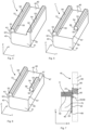
- Two pedestals 7a, b that are described in more detail in fig. 3-6 are connected to and protrude from the base 3. Without restriction to the specific example as shown, in a preferred embodiment, the pedestals 7a, b are arranged in a distance with a gap 2 in between.
- the gap 2 serves to accommodate electronic components, such as a directly modulated Laser (DML), in particular an assembly for carrying the electronic component.
- DML directly modulated Laser
- a submount 9 is attached on each of the pedestals 7a, 7b.
- an offset between pin 6 and a surface of submount 9 (pin offset, d1) is set between at least 0.05 mm and at most 0.2 mm.
- the minimum value of the pin offset is, according to a further preferred embodiment, at least 0.05 mm. This allows to first join pedestal 7a, b to base 3 in a first brazing process and subsequently joining submount 9 to pedestal 7a, b in a further, second brazing process without risking damage to submount 9.
- an offset d2 (submount offset) between a side face or edge of submount 9 and the base front face 58 is set between 0.1 mm and even 0 mm.
- the melted braze is drawn into a very small gap between these parts by capillary action. In this way, only a very small amount of excess brazing material 25 may be produced, resulting in only small brazing bulge 25. This further allows for a very tight and close connection with minimal or at least tightly controlled offset between adjoining parts.
- the submounts 9 are equally formed and are each mounted onto one of the pedestals 7a, b so that respective ends of conductor traces 13 that are connected to the pins 6 ideally face each other.
- a pattern of the structured conductor plating 13 of the submount 9 has a mirror symmetry. This enables to use submounts mounted with different ends pointing towards the base 3 and therewith have the ends 135 of the conductor traces 132 facing each other. This way, e.g. two submounts mounted on the pedestals 7a, b are of the same type but are simply mounted with one of the submounts turned around by 180°.
- the submounts 9 may have two opposite ends and are mounted with one end facing the base 3 and the other end facing the other submount 9, and wherein a symmetry plane of the mirror symmetrical conductor plating 13 may be located between the ends.
- the pedestals have a cuboid shape with six faces.
- the pedestal 7a, b therefore comprises a mounting face 40 for mounting or rather for brazing the mounting face 40 with the base front face 58 and a first 43 and second side face 44, as well as a free face 41 opposing the mounting face, an upper surface 42 for accommodating the submount 9 thereon, and a bottom face (not shown).
- Such embodiment has preferably a rectangular profile, which is in particular symmetrical with respect to at least three mirror planes. In this case, the side of the pedestal 7a, b with the mounting face 40 is plane.
- Bond wires to ground the conductor plating 13 or rather the submount 9 therefore must go down to the upper surface 42 of the pedestal 7a, b to get in contact with ground. This makes the bond wire longer. This may not be advantageous for very high frequency applications.
- this design is simple and also allows to use two equal pedestals. This embodiment is particularly suited for applications with lower signal rates to save costs.
- the pedestal is L-shaped with a bar 51, 53 arranged on the upper surface 42 and extending one of the side faces 43, 44.
- the bar may comprise a top face 54, a sidewall 55 and a side face 52 (not shown here), wherein the sidewall 55 is ideally arranged facing the submount 9 and in particular a height of the sidewall 55 is equal or at least similar to a height of the submount 9 so that the top face 54 of the bar 51, 53 and the conductor plating 13 are arranged coplanar.
- a width W1 of the top face 54 of the bar 51, 53 preferably represents the width W1 of the bar 51, 53.
- all faces are arranged in angle between 60° and 130°, especially the upper surface 42 is arranged to the mounting face 40 in angle between 80° and 100° and in particular 90°.
- the pedestal 7a, b shows an L-shaped pedestal 7a, b with a chamfer edge face 50 adjacent to the upper surface 42 and the mounting face 40.
- the pedestal may have chamfer edges 50, that are arranged at both ends, in particular one edge face 5o adjacent to the upper surface 42 and the mounting face 40 and one edge face 50 adjacent to the upper surface 42 and the free face 41 (not shown here).
- the bar 51, 53 may have the same height H1 as the submount 9/H2, or the ratio of the height H1 of the bar 51, 53 to the height H2 of the submount 9 is between 0.5 and 1.5.
- the height H1 of the protrusion is preferably between 0.1 mm and 0.5 mm. A typical height is about 0.2 mm.
- the width of the protrusion may be between 0.1 mm and 0.3 mm. A typical width is 0.175 mm.
- the L-shaped profile has several advantages. The ground is accessible easily from a top side of the pedestal submount 9. Because the bar is of solid metal and is as long as the pedestal submount 9 itself, this ground area has low inductance and is therefore preferred for RF application. Further, the bar 51, 52 serves as an electro-magnetic shielding. The EM-Field inside the pedestal submount 9 cannot extent over the pedestal 7a, b in negative Y-direction, as it is possible without sidewall 55.
- the shorter bar 53 may be arranged with a first 56 and a second end 57 distanced from both ends 40, 41 of the pedestal 7a, b.
- the shorter bar 53 is arranged centered between both ends 40, 41 of the pedestal 7a, b.
- the submount can be fabricated also symmetrical with a U-shaped profile and thus avoiding the costly production of different components.
- the submount 9 can be placed very precisely and very close, in particular almost in direct contact to the pin, so that the RF and/or electronic performance can be maximized. Furthermore, less costly soldering material is needed for the connection of the pin and the submount 9.
Landscapes
- Physics & Mathematics (AREA)
- Condensed Matter Physics & Semiconductors (AREA)
- General Physics & Mathematics (AREA)
- Electromagnetism (AREA)
- Optics & Photonics (AREA)
- Semiconductor Lasers (AREA)
- Shielding Devices Or Components To Electric Or Magnetic Fields (AREA)
Claims (9)
- Sockel (1) für optoelektronische Anwendungen, mit einer elektrisch leitfähigen Sockelbasis (3), die sich in Richtung einer Höhe (Z), einer Breite (X) und einer Länge (Y) erstreckt, und mit einer Sockelrückseite (59) und eine Sockelvorderseite (58) sowie mit mindestens zwei Öffnungen (8), die sich von der Sockelrückseite (59) durch das Volumen der Basis (3) hindurch und entlang der Breitenrichtung (X) zu der Sockelvorderseite (58) hin erstrecken, um pro Öffnung (8) mindestens einen elektrisch isolierten Stift (6) aufzunehmen, der durch die Öffnung (8) hindurch gesteckt wird, wobei an der Sockelvorderseite (58) spiegelsymmetrisch in Bezug auf eine imaginäre Ebene parallel zu der Höhen- (Z) und der Breitenrichtung (X) ein erstes und ein zweites elektrisch leitfähiges Podest (7a, 7b) angeordnet ist,wobei das erste und das zweite Podest (7a, 7b) in Höhenrichtung (Z) unterhalb einer Mitte einer jeweiligen Öffnung (8) angeordnet sind und jedes Podest (7a, 7b) zumindest eine Podestbefestigungsfläche (40) und eine zu der Podestbefestigungsfläche (40) entgegengesetzt gerichtete freie Podestfläche (41) aufweist, und mindestens eine Oberseite (42) zum Montieren und Tragen eines Podest-Submounts (9) sowie Podestseitenflächen aufweist, wobei die Oberseite (42) des Podests dem jeweiligen Stift (6) zugewandt ist,
dadurch gekennzeichnet, dassdie Podestbefestigungsfläche (40) des ersten und des zweiten Podests (7a, 7b) jeweils fest an der Vorderseite (58) der Basis angebracht ist, und zwar mit einem elektrisch leitfähigen Material, das zumindest teilweise zwischen der Vorderseite (58) der Basis und der Podestbefestigungsfläche (40) angeordnet ist, und dassjedes Podest (7a, 7b) einen Steg (51, 53) umfasst, der auf dessen Oberseite (42) angeordnet ist und senkrecht zu der Längs- (Y) und der Höhenrichtung (Z) ausgerichtet ist, und der Steg sich entlang einer der Seitenflächen (43, 44) des Podests erstreckt, um angrenzend an die Oberseite (42) eine Seitenwandung (55) zu bilden, wobei in einem Querschnitt entlang der Höhen- (Z) und der Längsrichtung (Y) des ersten (7a) und des zweiten (7b) Podests jeweils durch den ersten Steg (51) und die Oberseite (42) des Podests eine L-Form gebildet ist. - Sockel (1) nach Anspruch 1, dadurch gekennzeichnet, dass
die Oberseite (42) jedes Podests (7) mit der freien Fläche (41) und/oder der Befestigungsfläche (40) über eine Kante (49, 50) verbunden ist, wobei die Kante (49, 50) angrenzend an die und zwischen der Oberseite (42) und der Befestigungsfläche (40) und/oder der freien Fläche (41) angeordnet ist, wobei:- die Kante (49, 50) als Fasenkante ausgebildet ist oder- die Kante (49, 50) als Übergangskante ausgebildet ist. - Sockel (1) nach einem der vorhergehenden Ansprüche, dadurch gekennzeichnet, dass das erste (7a) und das zweite (7b) Podest jeweils einen zweiten Steg (53) umfassen, der an dessen Oberseite (42) angeordnet ist und senkrecht zu der Längs- (Y) und der Höhenrichtung (Z) ausgerichtet ist, und der zweite Steg (53) sich entlang einer zweiten Seitenfläche (44) des ersten (7a) und des zweiten (7b) Podests erstreckt, um angrenzend an die Oberseite (42) eine zweite Seitenwandung (55) zu bilden, wobei:- in einem Querschnitt entlang der Höhen- (Z) und der Längsrichtung (Y) des ersten (7a) und des zweiten (7b) Podests jeweils durch den ersten Steg (51), den zweiten Steg (53) und die Oberseite (42) des Podests eine U-Form gebildet ist, oder- ein Steg (51, 53) jedes Podests (7) eine geringere Länge aufweist als der andere Steg, um in einem Querschnitt entlang der Höhen- (Z) und der Längsrichtung (Y) des ersten (7a) und des zweiten (7b) Podests eine partielle U-Form zu bilden, wobei die Oberseite (42) zwischen dem ersten Steg (51) und dem zweiten Steg (53) angeordnet ist.
- Sockel (1) nach einem der vorhergehenden Ansprüche, dadurch gekennzeichnet, dass der Sockel (1) zwei Podest-Submounts (9) umfasst, die jeweils auf der Oberseite (42) des ersten (7a) und des zweiten (7b) Podests befestigt sind, wobei eine Höhe (H1) von mindestens einer Seitenwandung (55) ein Verhältnis zwischen 0,5 und 1,5 zu einer Höhe (H2) des Podest-Submounts (9) aufweist.
- Sockel (1) nach dem vorhergehenden Anspruch, dadurch gekennzeichnet, dass eine Länge (L1) des ersten (7a) und des zweiten (7b) Podests in der Längsrichtung (Y) größer ist als eine Länge (L2) der Podest-Submounts (9).
- Sockel (1) nach einem der vorhergehenden Ansprüche, dadurch gekennzeichnet, dass eine Höhe (H1) von mindestens einer Seitenwandung (55) größer ist als 0,1 mm, vorzugsweise größer als 0,2 mm, vorzugsweise größer als 0,3 mm, und/oder kleiner ist als 0,6 mm, vorzugsweise kleiner als 0,5 mm, vorzugsweise kleiner als 0,4 mm.
- Sockel (1) nach einem der Ansprüche 1 bis 5, dadurch gekennzeichnet, dass eine Breite (W1) zumindest eines Stegs (51, 53) größer ist als 0,05 mm, vorzugsweise größer als 0,1 mm, vorzugsweise größer als 0,15 mm, und/oder kleiner ist als 0,3 mm, vorzugsweise kleiner als 0,25 mm, vorzugsweise kleiner als 0,2 mm.
- Sockel (1) nach einem der vorhergehenden Ansprüche, dadurch gekennzeichnet, dass mindestens einer der Stifte (6) zumindest eines der folgenden Merkmale umfasst:- eine Kopffläche des Stifts (6) ist bündig mit der Vorderseite (2) des Sockels (3) angeordnet,- der Stift (6) umfasst einen Nagelkopf.
- Sockel (1) nach einem der vorhergehenden Ansprüche 4 bis 8,
dadurch gekennzeichnet, dass
eine Leiterbahn des jeweiligen auf der Oberseite (42) befestigten Submounts (9) elektrisch, insbesondere über ein elektrisch leitfähiges Material, mit mindestens einem Steg (51, 53) verbunden ist, der Teil eines koplanaren Wellenleiters ist.
Priority Applications (4)
| Application Number | Priority Date | Filing Date | Title |
|---|---|---|---|
| EP20194344.6A EP3965145B1 (de) | 2020-09-03 | 2020-09-03 | Transistorsockel für optoelektronisches hochgeschwindigkeits-gehäuse |
| US17/461,666 US12381370B2 (en) | 2020-09-03 | 2021-08-30 | Transistor outline header for high-speed data transmission of optoelectronic applications |
| JP2021143427A JP7258975B2 (ja) | 2020-09-03 | 2021-09-02 | 光電子用途の高速データ伝送用のトランジスタアウトラインヘッダ |
| CN202111030977.4A CN114221152B (zh) | 2020-09-03 | 2021-09-03 | 用于光电应用的高速数据传输的晶体管轮廓接头 |
Applications Claiming Priority (1)
| Application Number | Priority Date | Filing Date | Title |
|---|---|---|---|
| EP20194344.6A EP3965145B1 (de) | 2020-09-03 | 2020-09-03 | Transistorsockel für optoelektronisches hochgeschwindigkeits-gehäuse |
Publications (2)
| Publication Number | Publication Date |
|---|---|
| EP3965145A1 EP3965145A1 (de) | 2022-03-09 |
| EP3965145B1 true EP3965145B1 (de) | 2025-04-16 |
Family
ID=72355897
Family Applications (1)
| Application Number | Title | Priority Date | Filing Date |
|---|---|---|---|
| EP20194344.6A Active EP3965145B1 (de) | 2020-09-03 | 2020-09-03 | Transistorsockel für optoelektronisches hochgeschwindigkeits-gehäuse |
Country Status (4)
| Country | Link |
|---|---|
| US (1) | US12381370B2 (de) |
| EP (1) | EP3965145B1 (de) |
| JP (1) | JP7258975B2 (de) |
| CN (1) | CN114221152B (de) |
Families Citing this family (7)
| Publication number | Priority date | Publication date | Assignee | Title |
|---|---|---|---|---|
| JP7350646B2 (ja) * | 2019-12-17 | 2023-09-26 | CIG Photonics Japan株式会社 | 光モジュール |
| JP7382872B2 (ja) * | 2020-03-24 | 2023-11-17 | 新光電気工業株式会社 | 半導体パッケージ用ステム、半導体パッケージ |
| JP7382871B2 (ja) | 2020-03-24 | 2023-11-17 | 新光電気工業株式会社 | 半導体パッケージ用ステム、半導体パッケージ |
| EP3965146B1 (de) * | 2020-09-03 | 2025-04-09 | Schott Ag | Sockel für eine elektronische komponente |
| JP7507682B2 (ja) * | 2020-12-28 | 2024-06-28 | 新光電気工業株式会社 | 半導体パッケージ用ステム |
| WO2025182087A1 (ja) * | 2024-03-01 | 2025-09-04 | 三菱電機株式会社 | 光モジュール |
| JP7729512B1 (ja) * | 2024-03-01 | 2025-08-26 | 三菱電機株式会社 | 光モジュール |
Family Cites Families (43)
| Publication number | Priority date | Publication date | Assignee | Title |
|---|---|---|---|---|
| US5812582A (en) * | 1995-10-03 | 1998-09-22 | Methode Electronics, Inc. | Vertical cavity surface emitting laser feedback system and method |
| JP2000353846A (ja) | 1999-06-11 | 2000-12-19 | Toshiba Electronic Engineering Corp | ステム型半導体レーザ装置 |
| JP2001111152A (ja) | 1999-10-06 | 2001-04-20 | Rohm Co Ltd | 半導体レーザ |
| JP4074419B2 (ja) * | 2000-03-14 | 2008-04-09 | シャープ株式会社 | 半導体レーザ装置のワイヤボンディング方法 |
| JP3409781B2 (ja) | 2000-09-05 | 2003-05-26 | 住友電気工業株式会社 | 光半導体モジュールの製造方法 |
| JP3889933B2 (ja) | 2001-03-02 | 2007-03-07 | シャープ株式会社 | 半導体発光装置 |
| US6577656B2 (en) | 2001-03-13 | 2003-06-10 | Finisar Corporation | System and method of packaging a laser/detector |
| JP2003163512A (ja) | 2001-11-27 | 2003-06-06 | Kyocera Corp | 半導体素子収納用パッケージおよび半導体装置 |
| WO2003081735A1 (fr) * | 2002-03-25 | 2003-10-02 | Sanyo Electric Co., Ltd. | Dispositif a faisceau laser a semi-conducteurs |
| US6803520B1 (en) | 2002-05-03 | 2004-10-12 | Bookham Technology Plc | High speed to-package external interface |
| JP3998526B2 (ja) | 2002-07-12 | 2007-10-31 | 三菱電機株式会社 | 光半導体用パッケージ |
| JP4198410B2 (ja) | 2002-07-30 | 2008-12-17 | 三菱電機株式会社 | 光半導体集積装置 |
| DE10255462B4 (de) | 2002-11-25 | 2005-07-07 | Infineon Technologies Ag | Elektrische Anordnung und Verfahren zum Herstellen einer elektrischen Anordnung |
| KR100526504B1 (ko) | 2003-06-04 | 2005-11-08 | 삼성전자주식회사 | 광소자 모듈 패키지 및 그 제조 방법 |
| JP2005045234A (ja) * | 2003-07-09 | 2005-02-17 | Sumitomo Electric Ind Ltd | 発光モジュール |
| JP4583128B2 (ja) * | 2004-03-30 | 2010-11-17 | 三洋電機株式会社 | 半導体レーザ装置 |
| JP4815814B2 (ja) | 2005-02-04 | 2011-11-16 | 三菱電機株式会社 | 光モジュール |
| JP2006222145A (ja) | 2005-02-08 | 2006-08-24 | Sumitomo Electric Ind Ltd | レーザモジュール及び実装方法 |
| JP4671728B2 (ja) * | 2005-03-25 | 2011-04-20 | 三洋電機株式会社 | 半導体レーザ装置および光ピックアップ装置 |
| US7790484B2 (en) | 2005-06-08 | 2010-09-07 | Sharp Kabushiki Kaisha | Method for manufacturing laser devices |
| JP4970924B2 (ja) | 2006-03-28 | 2012-07-11 | 三菱電機株式会社 | 光素子用パッケージとこれを用いた光半導体装置 |
| JP5003110B2 (ja) | 2006-11-15 | 2012-08-15 | 住友電気工業株式会社 | 光電変換モジュール |
| JP2008130834A (ja) | 2006-11-21 | 2008-06-05 | Mitsubishi Electric Corp | 光モジュール |
| DE102007016692B3 (de) | 2007-04-04 | 2008-07-24 | Schott Ag | Metall-Fixiermaterial-Durchführung |
| JP2011203458A (ja) * | 2010-03-25 | 2011-10-13 | Sumitomo Electric Ind Ltd | 発光モジュール |
| CN103907249B (zh) | 2011-11-30 | 2015-02-25 | 松下电器产业株式会社 | 氮化物半导体发光装置 |
| JP6412274B2 (ja) | 2015-08-24 | 2018-10-24 | 京セラ株式会社 | 電子部品搭載用パッケージおよびそれを用いた電子装置 |
| JP7043048B2 (ja) | 2017-03-28 | 2022-03-29 | 株式会社Qdレーザ | レーザモジュール及び画像投影装置 |
| CN108988120A (zh) | 2017-06-02 | 2018-12-11 | 海信集团有限公司 | 同轴封装的激光器以及光模块 |
| CN107508141A (zh) | 2017-08-16 | 2017-12-22 | 青岛海信宽带多媒体技术有限公司 | 一种同轴封装的激光器及光模块 |
| US10819084B2 (en) * | 2017-06-02 | 2020-10-27 | Hisense Broadband Multimedia Technologies Co., Ltd. | TO-CAN packaged laser and optical module |
| JP2019029394A (ja) | 2017-07-26 | 2019-02-21 | 住友電気工業株式会社 | キャリア実装構造 |
| DE102017120216B4 (de) * | 2017-09-01 | 2019-05-23 | Schott Ag | TO-Gehäuse für einen DFB-Laser |
| CN108075350A (zh) | 2017-12-19 | 2018-05-25 | 深圳市东飞凌科技有限公司 | 同轴封装激光器 |
| CN108390255A (zh) | 2018-02-22 | 2018-08-10 | 青岛海信宽带多媒体技术有限公司 | 光学次模块及光模块 |
| EP3799229B1 (de) | 2018-05-21 | 2024-03-06 | Panasonic Intellectual Property Management Co., Ltd. | Halbleiterlaservorrichtung |
| CN110808491B (zh) | 2018-08-06 | 2022-06-24 | 富士康(昆山)电脑接插件有限公司 | 电连接器组件 |
| DE102018120895A1 (de) * | 2018-08-27 | 2020-02-27 | Schott Ag | TO-Gehäuse mit einem Erdanschluss |
| JP7136647B2 (ja) | 2018-09-27 | 2022-09-13 | 京セラ株式会社 | 電子部品搭載用パッケージおよびそれを用いた電子装置 |
| CN113169130B (zh) | 2018-11-30 | 2023-10-17 | 京瓷株式会社 | 布线基板、电子部件搭载用封装件以及电子装置 |
| JP7295634B2 (ja) * | 2018-12-17 | 2023-06-21 | 日本ルメンタム株式会社 | 光サブアッセンブリ及び光モジュール |
| FR3092206B1 (fr) | 2019-01-28 | 2021-10-15 | Raydiall | Connecteur pour carte de circuit imprimé muni d’un capot conducteur de fermeture de ligne de transmission de signaux électriques |
| JP7382871B2 (ja) | 2020-03-24 | 2023-11-17 | 新光電気工業株式会社 | 半導体パッケージ用ステム、半導体パッケージ |
-
2020
- 2020-09-03 EP EP20194344.6A patent/EP3965145B1/de active Active
-
2021
- 2021-08-30 US US17/461,666 patent/US12381370B2/en active Active
- 2021-09-02 JP JP2021143427A patent/JP7258975B2/ja active Active
- 2021-09-03 CN CN202111030977.4A patent/CN114221152B/zh active Active
Also Published As
| Publication number | Publication date |
|---|---|
| CN114221152B (zh) | 2024-11-22 |
| EP3965145A1 (de) | 2022-03-09 |
| CN114221152A (zh) | 2022-03-22 |
| JP2022043009A (ja) | 2022-03-15 |
| US20220069544A1 (en) | 2022-03-03 |
| US12381370B2 (en) | 2025-08-05 |
| JP7258975B2 (ja) | 2023-04-17 |
Similar Documents
| Publication | Publication Date | Title |
|---|---|---|
| EP3965145B1 (de) | Transistorsockel für optoelektronisches hochgeschwindigkeits-gehäuse | |
| US7217958B2 (en) | Feed through structure for optical semiconductor package | |
| US10763638B2 (en) | Transistor outline housings for distributed feedback lasers | |
| JP7690539B2 (ja) | 電子部品または光電子部品用のヘッダおよびこのようなヘッダを製造するための方法 | |
| US11367992B2 (en) | Housing for an electronic component, and laser module | |
| US12230937B2 (en) | Header for an electric component | |
| US11923652B2 (en) | Header for semiconductor package, and semiconductor package | |
| JP4212845B2 (ja) | 光半導体素子モジュール | |
| US20020196820A1 (en) | Semiconductor laser device for optical communication | |
| KR102814390B1 (ko) | 광 반도체 장치 | |
| US20230359024A1 (en) | Optical device, subassembly of optical device, and method of manufacturing optical device | |
| US7192201B2 (en) | Optical transmitting module having a de-coupling inductor therein | |
| US11955403B2 (en) | Header for semiconductor package and semiconductor package | |
| JP3619473B2 (ja) | 半導体素子収納用パッケージ | |
| EP4704270A1 (de) | Laserdiodenkopfteil mit thermoelektrischer steuerung | |
| JP7745811B1 (ja) | Can型光モジュール | |
| TW202545097A (zh) | 光模組 |
Legal Events
| Date | Code | Title | Description |
|---|---|---|---|
| STAA | Information on the status of an ep patent application or granted ep patent |
Free format text: STATUS: EXAMINATION IS IN PROGRESS |
|
| PUAI | Public reference made under article 153(3) epc to a published international application that has entered the european phase |
Free format text: ORIGINAL CODE: 0009012 |
|
| 17P | Request for examination filed |
Effective date: 20200903 |
|
| AK | Designated contracting states |
Kind code of ref document: A1 Designated state(s): AL AT BE BG CH CY CZ DE DK EE ES FI FR GB GR HR HU IE IS IT LI LT LU LV MC MK MT NL NO PL PT RO RS SE SI SK SM TR |
|
| RBV | Designated contracting states (corrected) |
Designated state(s): AL AT BE BG CH CY CZ DE DK EE ES FI FR GB GR HR HU IE IS IT LI LT LU LV MC MK MT NL NO PL PT RO RS SE SI SK SM TR |
|
| P01 | Opt-out of the competence of the unified patent court (upc) registered |
Effective date: 20230516 |
|
| GRAP | Despatch of communication of intention to grant a patent |
Free format text: ORIGINAL CODE: EPIDOSNIGR1 |
|
| STAA | Information on the status of an ep patent application or granted ep patent |
Free format text: STATUS: GRANT OF PATENT IS INTENDED |
|
| RIC1 | Information provided on ipc code assigned before grant |
Ipc: H01S 5/0235 20210101ALI20241205BHEP Ipc: H01S 5/0233 20210101ALI20241205BHEP Ipc: H01S 5/02212 20210101ALI20241205BHEP Ipc: H01L 23/10 20060101ALI20241205BHEP Ipc: H01S 5/022 20210101ALI20241205BHEP Ipc: G02B 6/42 20060101ALI20241205BHEP Ipc: H01S 5/023 20210101ALI20241205BHEP Ipc: H01L 23/04 20060101AFI20241205BHEP |
|
| GRAJ | Information related to disapproval of communication of intention to grant by the applicant or resumption of examination proceedings by the epo deleted |
Free format text: ORIGINAL CODE: EPIDOSDIGR1 |
|
| STAA | Information on the status of an ep patent application or granted ep patent |
Free format text: STATUS: EXAMINATION IS IN PROGRESS |
|
| INTG | Intention to grant announced |
Effective date: 20241219 |
|
| RIN1 | Information on inventor provided before grant (corrected) |
Inventor name: KRAUSE, ANDREAS Inventor name: SOON, AMY Inventor name: TAN, JIAN DEAN Inventor name: WAI LI, ONG Inventor name: AOWUDOMSUK, ARTIT Inventor name: DROEGEMUELLER, KARSTEN |
|
| GRAP | Despatch of communication of intention to grant a patent |
Free format text: ORIGINAL CODE: EPIDOSNIGR1 |
|
| STAA | Information on the status of an ep patent application or granted ep patent |
Free format text: STATUS: GRANT OF PATENT IS INTENDED |
|
| INTC | Intention to grant announced (deleted) | ||
| INTG | Intention to grant announced |
Effective date: 20250131 |
|
| GRAS | Grant fee paid |
Free format text: ORIGINAL CODE: EPIDOSNIGR3 |
|
| GRAA | (expected) grant |
Free format text: ORIGINAL CODE: 0009210 |
|
| STAA | Information on the status of an ep patent application or granted ep patent |
Free format text: STATUS: THE PATENT HAS BEEN GRANTED |
|
| AK | Designated contracting states |
Kind code of ref document: B1 Designated state(s): AL AT BE BG CH CY CZ DE DK EE ES FI FR GB GR HR HU IE IS IT LI LT LU LV MC MK MT NL NO PL PT RO RS SE SI SK SM TR |
|
| REG | Reference to a national code |
Ref country code: GB Ref legal event code: FG4D |
|
| REG | Reference to a national code |
Ref country code: CH Ref legal event code: EP Ref country code: DE Ref legal event code: R096 Ref document number: 602020049450 Country of ref document: DE |
|
| REG | Reference to a national code |
Ref country code: IE Ref legal event code: FG4D |
|
| REG | Reference to a national code |
Ref country code: NL Ref legal event code: MP Effective date: 20250416 |
|
| PG25 | Lapsed in a contracting state [announced via postgrant information from national office to epo] |
Ref country code: NL Free format text: LAPSE BECAUSE OF FAILURE TO SUBMIT A TRANSLATION OF THE DESCRIPTION OR TO PAY THE FEE WITHIN THE PRESCRIBED TIME-LIMIT Effective date: 20250416 |
|
| REG | Reference to a national code |
Ref country code: AT Ref legal event code: MK05 Ref document number: 1786391 Country of ref document: AT Kind code of ref document: T Effective date: 20250416 |
|
| PG25 | Lapsed in a contracting state [announced via postgrant information from national office to epo] |
Ref country code: ES Free format text: LAPSE BECAUSE OF FAILURE TO SUBMIT A TRANSLATION OF THE DESCRIPTION OR TO PAY THE FEE WITHIN THE PRESCRIBED TIME-LIMIT Effective date: 20250416 Ref country code: FI Free format text: LAPSE BECAUSE OF FAILURE TO SUBMIT A TRANSLATION OF THE DESCRIPTION OR TO PAY THE FEE WITHIN THE PRESCRIBED TIME-LIMIT Effective date: 20250416 Ref country code: PT Free format text: LAPSE BECAUSE OF FAILURE TO SUBMIT A TRANSLATION OF THE DESCRIPTION OR TO PAY THE FEE WITHIN THE PRESCRIBED TIME-LIMIT Effective date: 20250818 |
|
| PGFP | Annual fee paid to national office [announced via postgrant information from national office to epo] |
Ref country code: DE Payment date: 20250919 Year of fee payment: 6 |
|
| REG | Reference to a national code |
Ref country code: LT Ref legal event code: MG9D |
|
| PG25 | Lapsed in a contracting state [announced via postgrant information from national office to epo] |
Ref country code: NO Free format text: LAPSE BECAUSE OF FAILURE TO SUBMIT A TRANSLATION OF THE DESCRIPTION OR TO PAY THE FEE WITHIN THE PRESCRIBED TIME-LIMIT Effective date: 20250716 Ref country code: GR Free format text: LAPSE BECAUSE OF FAILURE TO SUBMIT A TRANSLATION OF THE DESCRIPTION OR TO PAY THE FEE WITHIN THE PRESCRIBED TIME-LIMIT Effective date: 20250717 |
|
| PG25 | Lapsed in a contracting state [announced via postgrant information from national office to epo] |
Ref country code: PL Free format text: LAPSE BECAUSE OF FAILURE TO SUBMIT A TRANSLATION OF THE DESCRIPTION OR TO PAY THE FEE WITHIN THE PRESCRIBED TIME-LIMIT Effective date: 20250416 |
|
| PG25 | Lapsed in a contracting state [announced via postgrant information from national office to epo] |
Ref country code: BG Free format text: LAPSE BECAUSE OF FAILURE TO SUBMIT A TRANSLATION OF THE DESCRIPTION OR TO PAY THE FEE WITHIN THE PRESCRIBED TIME-LIMIT Effective date: 20250416 |
|
| PG25 | Lapsed in a contracting state [announced via postgrant information from national office to epo] |
Ref country code: HR Free format text: LAPSE BECAUSE OF FAILURE TO SUBMIT A TRANSLATION OF THE DESCRIPTION OR TO PAY THE FEE WITHIN THE PRESCRIBED TIME-LIMIT Effective date: 20250416 |
|
| PG25 | Lapsed in a contracting state [announced via postgrant information from national office to epo] |
Ref country code: AT Free format text: LAPSE BECAUSE OF FAILURE TO SUBMIT A TRANSLATION OF THE DESCRIPTION OR TO PAY THE FEE WITHIN THE PRESCRIBED TIME-LIMIT Effective date: 20250416 |
|
| PG25 | Lapsed in a contracting state [announced via postgrant information from national office to epo] |
Ref country code: RS Free format text: LAPSE BECAUSE OF FAILURE TO SUBMIT A TRANSLATION OF THE DESCRIPTION OR TO PAY THE FEE WITHIN THE PRESCRIBED TIME-LIMIT Effective date: 20250716 |
|
| PG25 | Lapsed in a contracting state [announced via postgrant information from national office to epo] |
Ref country code: IS Free format text: LAPSE BECAUSE OF FAILURE TO SUBMIT A TRANSLATION OF THE DESCRIPTION OR TO PAY THE FEE WITHIN THE PRESCRIBED TIME-LIMIT Effective date: 20250816 |
|
| PG25 | Lapsed in a contracting state [announced via postgrant information from national office to epo] |
Ref country code: LV Free format text: LAPSE BECAUSE OF FAILURE TO SUBMIT A TRANSLATION OF THE DESCRIPTION OR TO PAY THE FEE WITHIN THE PRESCRIBED TIME-LIMIT Effective date: 20250416 |
|
| REG | Reference to a national code |
Ref country code: DE Ref legal event code: R079 Ref document number: 602020049450 Country of ref document: DE Free format text: PREVIOUS MAIN CLASS: H01L0023040000 Ipc: H10W0076120000 |
|
| PG25 | Lapsed in a contracting state [announced via postgrant information from national office to epo] |
Ref country code: SM Free format text: LAPSE BECAUSE OF FAILURE TO SUBMIT A TRANSLATION OF THE DESCRIPTION OR TO PAY THE FEE WITHIN THE PRESCRIBED TIME-LIMIT Effective date: 20250416 Ref country code: DK Free format text: LAPSE BECAUSE OF FAILURE TO SUBMIT A TRANSLATION OF THE DESCRIPTION OR TO PAY THE FEE WITHIN THE PRESCRIBED TIME-LIMIT Effective date: 20250416 |
|
| REG | Reference to a national code |
Ref country code: DE Ref legal event code: R097 Ref document number: 602020049450 Country of ref document: DE |
|
| PG25 | Lapsed in a contracting state [announced via postgrant information from national office to epo] |
Ref country code: CZ Free format text: LAPSE BECAUSE OF FAILURE TO SUBMIT A TRANSLATION OF THE DESCRIPTION OR TO PAY THE FEE WITHIN THE PRESCRIBED TIME-LIMIT Effective date: 20250416 |
|
| PG25 | Lapsed in a contracting state [announced via postgrant information from national office to epo] |
Ref country code: EE Free format text: LAPSE BECAUSE OF FAILURE TO SUBMIT A TRANSLATION OF THE DESCRIPTION OR TO PAY THE FEE WITHIN THE PRESCRIBED TIME-LIMIT Effective date: 20250416 |
|
| PG25 | Lapsed in a contracting state [announced via postgrant information from national office to epo] |
Ref country code: RO Free format text: LAPSE BECAUSE OF FAILURE TO SUBMIT A TRANSLATION OF THE DESCRIPTION OR TO PAY THE FEE WITHIN THE PRESCRIBED TIME-LIMIT Effective date: 20250416 Ref country code: SK Free format text: LAPSE BECAUSE OF FAILURE TO SUBMIT A TRANSLATION OF THE DESCRIPTION OR TO PAY THE FEE WITHIN THE PRESCRIBED TIME-LIMIT Effective date: 20250416 |
|
| PG25 | Lapsed in a contracting state [announced via postgrant information from national office to epo] |
Ref country code: IT Free format text: LAPSE BECAUSE OF FAILURE TO SUBMIT A TRANSLATION OF THE DESCRIPTION OR TO PAY THE FEE WITHIN THE PRESCRIBED TIME-LIMIT Effective date: 20250416 |
|
| PLBE | No opposition filed within time limit |
Free format text: ORIGINAL CODE: 0009261 |
|
| STAA | Information on the status of an ep patent application or granted ep patent |
Free format text: STATUS: NO OPPOSITION FILED WITHIN TIME LIMIT |
|
| REG | Reference to a national code |
Ref country code: CH Ref legal event code: L10 Free format text: ST27 STATUS EVENT CODE: U-0-0-L10-L00 (AS PROVIDED BY THE NATIONAL OFFICE) Effective date: 20260225 |
|
| 26N | No opposition filed |
Effective date: 20260119 |