EP3926662B1 - Onium salt-containing processing solution for semiconductor wafers - Google Patents
Onium salt-containing processing solution for semiconductor wafers Download PDFInfo
- Publication number
- EP3926662B1 EP3926662B1 EP20756178.8A EP20756178A EP3926662B1 EP 3926662 B1 EP3926662 B1 EP 3926662B1 EP 20756178 A EP20756178 A EP 20756178A EP 3926662 B1 EP3926662 B1 EP 3926662B1
- Authority
- EP
- European Patent Office
- Prior art keywords
- ion
- treatment liquid
- ruthenium
- hypochlorite
- etching
- Prior art date
- Legal status (The legal status is an assumption and is not a legal conclusion. Google has not performed a legal analysis and makes no representation as to the accuracy of the status listed.)
- Active
Links
Images

Classifications
-
- C—CHEMISTRY; METALLURGY
- C09—DYES; PAINTS; POLISHES; NATURAL RESINS; ADHESIVES; COMPOSITIONS NOT OTHERWISE PROVIDED FOR; APPLICATIONS OF MATERIALS NOT OTHERWISE PROVIDED FOR
- C09K—MATERIALS FOR MISCELLANEOUS APPLICATIONS, NOT PROVIDED FOR ELSEWHERE
- C09K13/00—Etching, surface-brightening or pickling compositions
-
- C—CHEMISTRY; METALLURGY
- C09—DYES; PAINTS; POLISHES; NATURAL RESINS; ADHESIVES; COMPOSITIONS NOT OTHERWISE PROVIDED FOR; APPLICATIONS OF MATERIALS NOT OTHERWISE PROVIDED FOR
- C09K—MATERIALS FOR MISCELLANEOUS APPLICATIONS, NOT PROVIDED FOR ELSEWHERE
- C09K13/00—Etching, surface-brightening or pickling compositions
- C09K13/04—Etching, surface-brightening or pickling compositions containing an inorganic acid
- C09K13/06—Etching, surface-brightening or pickling compositions containing an inorganic acid with organic material
-
- C—CHEMISTRY; METALLURGY
- C07—ORGANIC CHEMISTRY
- C07C—ACYCLIC OR CARBOCYCLIC COMPOUNDS
- C07C211/00—Compounds containing amino groups bound to a carbon skeleton
- C07C211/62—Quaternary ammonium compounds
- C07C211/63—Quaternary ammonium compounds having quaternised nitrogen atoms bound to acyclic carbon atoms
-
- C—CHEMISTRY; METALLURGY
- C07—ORGANIC CHEMISTRY
- C07C—ACYCLIC OR CARBOCYCLIC COMPOUNDS
- C07C381/00—Compounds containing carbon and sulfur and having functional groups not covered by groups C07C301/00 - C07C337/00
- C07C381/12—Sulfonium compounds
-
- C—CHEMISTRY; METALLURGY
- C07—ORGANIC CHEMISTRY
- C07F—ACYCLIC, CARBOCYCLIC OR HETEROCYCLIC COMPOUNDS CONTAINING ELEMENTS OTHER THAN CARBON, HYDROGEN, HALOGEN, OXYGEN, NITROGEN, SULFUR, SELENIUM OR TELLURIUM
- C07F9/00—Compounds containing elements of Groups 5 or 15 of the Periodic Table
- C07F9/02—Phosphorus compounds
- C07F9/28—Phosphorus compounds with one or more P—C bonds
- C07F9/54—Quaternary phosphonium compounds
- C07F9/5442—Aromatic phosphonium compounds (P-C aromatic linkage)
-
- C—CHEMISTRY; METALLURGY
- C23—COATING METALLIC MATERIAL; COATING MATERIAL WITH METALLIC MATERIAL; CHEMICAL SURFACE TREATMENT; DIFFUSION TREATMENT OF METALLIC MATERIAL; COATING BY VACUUM EVAPORATION, BY SPUTTERING, BY ION IMPLANTATION OR BY CHEMICAL VAPOUR DEPOSITION, IN GENERAL; INHIBITING CORROSION OF METALLIC MATERIAL OR INCRUSTATION IN GENERAL
- C23F—NON-MECHANICAL REMOVAL OF METALLIC MATERIAL FROM SURFACE; INHIBITING CORROSION OF METALLIC MATERIAL OR INCRUSTATION IN GENERAL; MULTI-STEP PROCESSES FOR SURFACE TREATMENT OF METALLIC MATERIAL INVOLVING AT LEAST ONE PROCESS PROVIDED FOR IN CLASS C23 AND AT LEAST ONE PROCESS COVERED BY SUBCLASS C21D OR C22F OR CLASS C25
- C23F1/00—Etching metallic material by chemical means
- C23F1/10—Etching compositions
- C23F1/14—Aqueous compositions
- C23F1/32—Alkaline compositions
- C23F1/40—Alkaline compositions for etching other metallic material
-
- C—CHEMISTRY; METALLURGY
- C23—COATING METALLIC MATERIAL; COATING MATERIAL WITH METALLIC MATERIAL; CHEMICAL SURFACE TREATMENT; DIFFUSION TREATMENT OF METALLIC MATERIAL; COATING BY VACUUM EVAPORATION, BY SPUTTERING, BY ION IMPLANTATION OR BY CHEMICAL VAPOUR DEPOSITION, IN GENERAL; INHIBITING CORROSION OF METALLIC MATERIAL OR INCRUSTATION IN GENERAL
- C23F—NON-MECHANICAL REMOVAL OF METALLIC MATERIAL FROM SURFACE; INHIBITING CORROSION OF METALLIC MATERIAL OR INCRUSTATION IN GENERAL; MULTI-STEP PROCESSES FOR SURFACE TREATMENT OF METALLIC MATERIAL INVOLVING AT LEAST ONE PROCESS PROVIDED FOR IN CLASS C23 AND AT LEAST ONE PROCESS COVERED BY SUBCLASS C21D OR C22F OR CLASS C25
- C23F1/00—Etching metallic material by chemical means
- C23F1/46—Regeneration of etching compositions
-
- H—ELECTRICITY
- H10—SEMICONDUCTOR DEVICES; ELECTRIC SOLID-STATE DEVICES NOT OTHERWISE PROVIDED FOR
- H10P—GENERIC PROCESSES OR APPARATUS FOR THE MANUFACTURE OR TREATMENT OF DEVICES COVERED BY CLASS H10
- H10P50/00—Etching of wafers, substrates or parts of devices
- H10P50/60—Wet etching
- H10P50/66—Wet etching of conductive or resistive materials
- H10P50/663—Wet etching of conductive or resistive materials by chemical means only
- H10P50/667—Wet etching of conductive or resistive materials by chemical means only by liquid etching only
-
- H—ELECTRICITY
- H10—SEMICONDUCTOR DEVICES; ELECTRIC SOLID-STATE DEVICES NOT OTHERWISE PROVIDED FOR
- H10P—GENERIC PROCESSES OR APPARATUS FOR THE MANUFACTURE OR TREATMENT OF DEVICES COVERED BY CLASS H10
- H10P52/00—Grinding, lapping or polishing of wafers, substrates or parts of devices
-
- H—ELECTRICITY
- H10—SEMICONDUCTOR DEVICES; ELECTRIC SOLID-STATE DEVICES NOT OTHERWISE PROVIDED FOR
- H10W—GENERIC PACKAGES, INTERCONNECTIONS, CONNECTORS OR OTHER CONSTRUCTIONAL DETAILS OF DEVICES COVERED BY CLASS H10
- H10W20/00—Interconnections in chips, wafers or substrates
- H10W20/01—Manufacture or treatment
- H10W20/031—Manufacture or treatment of conductive parts of the interconnections
- H10W20/056—Manufacture or treatment of conductive parts of the interconnections by filling conductive material into holes, grooves or trenches
-
- H—ELECTRICITY
- H10—SEMICONDUCTOR DEVICES; ELECTRIC SOLID-STATE DEVICES NOT OTHERWISE PROVIDED FOR
- H10W—GENERIC PACKAGES, INTERCONNECTIONS, CONNECTORS OR OTHER CONSTRUCTIONAL DETAILS OF DEVICES COVERED BY CLASS H10
- H10W20/00—Interconnections in chips, wafers or substrates
- H10W20/40—Interconnections external to wafers or substrates, e.g. back-end-of-line [BEOL] metallisations or vias connecting to gate electrodes
- H10W20/41—Interconnections external to wafers or substrates, e.g. back-end-of-line [BEOL] metallisations or vias connecting to gate electrodes characterised by their conductive parts
- H10W20/44—Conductive materials thereof
- H10W20/4403—Conductive materials thereof based on metals, e.g. alloys, metal silicides
- H10W20/4432—Conductive materials thereof based on metals, e.g. alloys, metal silicides the principal metal being a noble metal, e.g. gold
Definitions
- the present invention relates to a novel treatment liquid for etching metallic ruthenium present on a semiconductor wafer to be used in a manufacturing process of a semiconductor element.
- a desired wiring material is a wiring material having more solid electromigration resistance and a lower electric resistance value than conventional wiring materials.
- Ruthenium has higher electromigration resistance than aluminum and copper which are conventional wiring materials, and ruthenium can decrease the electric resistance value of the wiring, thus attracting attention particularly as a wiring material for which the design rule for semiconductor elements is 10 nm or less. Not only in cases where ruthenium is used as a wiring material but also in cases where copper is used as a wiring material, ruthenium can prevent electromigration, and thus, using ruthenium as a barrier metal for copper wiring is under study.
- the wiring is formed by dry or wet etching in the same manner as in cases where a conventional wiring material is used.
- dry etching with an etching gas, or by CMP polishing, more precise etching is desired, and specifically, wet etching is attracting attention.
- Patent Document 1 as an etching method for a ruthenium film, a method for etching a ruthenium film using a chemical liquid having a pH of 12 or more and an oxidation-reduction potential of 300 mV vs SHE or more, specifically a solution of a halogen oxoate, such as hypochlorite, chlorite, and bromate, is presented.
- a chemical liquid that is for surely removing an adhered ruthenium by etching, and is designed for removing ruthenium.
- Patent Document 2 proposes a method for oxidizing ruthenium thereby dissolving and removing the ruthenium by using an aqueous solution of pH 11 or higher containing orthoperiodic acid.
- Patent Document 3 proposes an etching liquid for ruthenium metal having a pH of 10 or more and less than 12 containing a bromine-containing compound, an oxidizing agent, a basic compound, and water.
- Patent Document 4 proposes a cleaning method in which ruthenium is oxidized, thereby dissolved, and removed using a removal solution containing cerium (IV) ammonium nitrate and additionally a strong acid such as nitric acid.
- RuO 4 - or RuO 4 2- is changed to RuO 4 in a treatment liquid, and part of the same is gasified and released into a gas phase.
- RuO 4 is strongly oxidative, and thus, not only is harmful to the human body but also is easily reduced to generate RuO 2 particles. In general, particles cause a decrease in the yield rate, which constitutes a serious problem in semiconductor formation steps. Against such a background, it is very important to inhibit the generation of a RuO 4 gas.
- Patent Document 5 describes a chemical liquid having a pH of 12 or higher and an oxidation-reduction potential of 300 mV vs. SHE or higher as an etching liquid for a ruthenium film.
- a method for etching a ruthenium film using a solution of a halogen oxoate, such as hypochlorite, chlorite, and bromate is disclosed.
- Patent Document 6 proposes a method of oxidizing, thereby dissolving, and removing ruthenium by using an aqueous solution containing orthoperiodic acid having a pH of 11 or higher.
- Patent Document 7 describes a CMP slurry containing a ruthenium-coordinated nitrogen oxide ligand (N-O ligand) that does not generate a RuO 4 gas in chemical mechanical polishing (CMP) of ruthenium.
- N-O ligand ruthenium-coordinated nitrogen oxide ligand
- Patent Documents 8-10 disclose the etching of ruthenium with treatment liquids comprising hypochlorite ions.
- the method for etching ruthenium described in Patent Document 1 or 4 is intended to remove a ruthenium residue adhered to the back surface or bevels of a semiconductor substrate, and is capable of dissolving and removing ruthenium.
- the etching liquid described in Patent Document 1 or 4 it was difficult to maintain the desired flatness of the ruthenium surface after the etching treatment in the wiring step. Therefore, it was difficult to use the etching liquid according to Patent Document 1 or 4 as that for ruthenium in the step of forming the wiring of a semiconductor element.
- the etching liquid described in Patent Document 2 was an etching liquid targeting an etching residue containing ruthenium similarly as in Patent Document 1, and since it was difficult to maintain the flatness of the ruthenium surface after the etching treatment, the same could hardly be used in the step of forming the wiring.
- the first object of the present invention is to provide a treatment liquid that can wet-etch ruthenium present on a semiconductor wafer. Another object is to provide a treatment liquid that can maintain the flatness of the ruthenium surface after the etching treatment.
- Patent Document 5 the method of etching ruthenium described in Patent Document 5 is intended to remove ruthenium residues adhered to the back surface or bevels of a semiconductor substrate, and it is possible to dissolve and remove ruthenium.
- Patent Document 5 does not mention anything about the inhibition of a RuO 4 gas, and in fact, the method described in Patent Document 5 lacked stability, and was not able to inhibit generation of a RuO 4 gas, and a large amount of RuO 4 gas was generated. There was also a problem in that a large amount of RuO 2 (particles) was generated.
- Patent Document 6 discloses a ruthenium removal composition containing orthoperiodic acid, which can etch an etching residue containing ruthenium.
- Patent Document 6 does not mention anything about the inhibition of a RuO 4 gas, and a RuO 4 gas generated during the etching treatment could not be inhibited.
- Patent Document 7 shows that it is possible to inhibit a toxic RuO 4 gas by using a CMP slurry containing a ruthenium-coordinated nitrogen oxide ligand (N-O ligand) in performing CMP.
- N-O ligand ruthenium-coordinated nitrogen oxide ligand
- Patent Document 7 under alkaline conditions where the dissolution mechanism of ruthenium is different.
- the ruthenium-coordinated nitrogen oxide ligand described in Patent Document 7 was added to an alkaline ruthenium etching liquid containing hypochlorous acid, a RuO 4 gas was generated to confirm that there was no RuO 4 gas inhibitory effect.
- the present inventors diligently conducted investigations to achieve the first object above. For this purpose, the effect of addition of a specific alkylammonium salt to a treatment liquid containing hypochlorite ions was examined. Since the flatness of the ruthenium surface after the etching treatment could not be maintained with the treatment liquid containing only hypochlorite ions, various additive ingredients were combined. As a result, it was found that it became possible to maintain the flatness of the ruthenium surface after the etching treatment by adding a specific alkylammonium salt, thereby completing the first invention.
- a first aspect of the present invention for achieving the first object described above includes the treatment liquid according to claim 1 and the etching method according to claim 5. Embodiments and variants derive from the dependent claims.
- the treatment liquid of the first aspect of the present invention maintains the flatness of the ruthenium surface after the etching treatment
- alkylammonium ions of the alkylammonium salt contained in the treatment liquid adhere to the surface of ruthenium, which is the etching target, and form a protective layer.
- the protective layer formed from alkylammonium ions prevents a contact with hypochlorite ions, which oxidize and dissolve ruthenium, so that the flatness of the ruthenium surface after the etching treatment can be conceivably better maintained compared to an etching treatment with a treatment liquid containing solely hypochlorite ions.
- ruthenium can be wet-etched in a forming process of a semiconductor element, and furthermore, the flatness of the ruthenium surface after the etching treatment can be maintained. Therefore, it is suitable for use in the formation of a semiconductor element having a multilayer wiring structure, for which the flatness of each layer is required.
- the treatment liquid of the first aspect of the present invention gives excellent flatness of the ruthenium surface after the etching treatment, the ruthenium surface in contact with the treatment liquid can be etched evenly. Especially, even in the formation of a semiconductor element with a wiring structure with a dimension of 10 nm or less, where precise etching of ruthenium at several nanometer level is required, since the ruthenium surface in contact with the treatment liquid can be etched notably evenly, the treatment liquid can be used favorably.
- the treatment liquid of the first aspect of the present invention is capable of etching ruthenium at an etching rate of 20 ⁇ /min or higher. With an etching rate of 20 ⁇ /min or higher, it can be used satisfactorily in the process of forming a semiconductor element.
- ruthenium also expressed as Ru
- ruthenium is not limited to a ruthenium metal, insofar as the ruthenium element is included.
- the treatment liquid of the first aspect of the present invention is a treatment liquid that can etch ruthenium present on a semiconductor wafer without damaging the semiconductor wafer. Therefore, the treatment liquid of the first aspect of the present invention is a treatment liquid that can be suitably used in the wiring formation step in the semiconductor manufacturing process.
- the ruthenium to which the treatment liquid of the first aspect of the present invention is applied is mainly formed by a publicly known method, such as CVD, ALD, and a sputtering method, used in the semiconductor element process. Through etching the formed ruthenium, the wiring is formed in the semiconductor.
- FIGs. 1 and 2 show an example of the wiring formation step.
- a substrate 1 made of a semiconductor e.g. Si
- the prepared substrate is subjected to an oxidation treatment to form a silicon oxide film on the substrate.
- an interlayer insulating film 2 constituted with a low dielectric constant (low-k) film is formed, and in which via holes are formed at predetermined intervals.
- the via holes are filled with ruthenium 3 by thermal CVD, and a ruthenium film is further deposited thereon ( FIG. 1 ).
- the ruthenium film is etched and planarized by dry etching or wet etching to form the ruthenium wiring ( FIG. 2 ).
- the treatment liquid of the first aspect of the present invention contains (A) a hypochlorite ion, and (B) an alkylammonium salt expressed by the following Formula (1).
- A a hypochlorite ion
- B an alkylammonium salt expressed by the following Formula (1).
- the following is a step by step description.
- X - is a fluoride ion, a chloride ion, an iodide ion, a hydroxide ion, a nitrate ion, a phosphate ion, a sulfate ion, a hydrogen sulfate ion, a methanesulfate ion, a perchlorate ion, an acetate ion, a fluoroborate ion, or a trifluoroacetate ion.
- hypochlorite ion it is possible to generate hypochlorous acid and hypochlorite ions by dissolving hypochlorite in water.
- the hypochlorite ion is an oxidizing agent with strong oxidizability, and the treatment liquid of the present invention containing hypochlorite ions can etch a metal contained in a semiconductor wafer.
- the concentration of hypochlorite ions is preferably in a range of 0.05 to 20 mass% with respect to the total treatment liquid.
- the concentration of hypochlorite ions is preferably in a range of 0.1 to 15 mass%, more preferably 0.3 to 10 mass%, further preferably 0.5 to 6 mass%, and especially preferably 0.5 to 4 mass%.
- the concentration of hypochlorite ions in a treatment liquid of the first aspect of the present invention can be calculated at the time of the production of the treatment liquid, or can be affirmed by a direct analysis of the treatment liquid.
- the concentration of hypochlorite ions described in Example below was determined by measuring the effective chlorine concentration of the treatment liquid. Specifically, referring to Ministry of Health, Labour and Welfare Notification No. 318 (final revision on 11 March 2005), potassium iodide and acetic acid were added to a solution containing hypochlorite ions, the liberated iodine was redox-titrated with an aqueous solution of sodium thiosulfate, and the effective chlorine concentration was calculated.
- the concentration of hypochlorite ions of the present invention is obtained by converting from the calculated effective chlorine concentration.
- the alkylammonium salt contained in a treatment liquid of the first aspect of the present invention is the alkylammonium salt expressed by the following Formula (1).
- X - is a fluoride ion, a chloride ion, an iodide ion, a hydroxide ion, a nitrate ion, a phosphate ion, a sulfate ion, a hydrogen sulfate ion, a methanesulfate ion, a perchlorate ion, an acetate ion, a fluoroborate ion, or a trifluoroacetate ion.
- the integer “a” in the above Formula (1) represents the number of methylene groups, and those in which the integer “a” is from 6 to 20 can be used without any particular restriction, and the integer “a” is more preferably from 6 to 15, and further preferably from 8 to 13.
- An alkylammonium salt having methylene groups within the aforedescribed range can be adsorbed onto the ruthenium surface to form an appropriate protective layer, and therefore can be favorably used.
- the integer “a” of the alkylammonium salt is larger, the amount of alkylammonium ions of the alkylammonium salt adsorbed onto the ruthenium surface increases, and therefore the etching rate of ruthenium tends to decrease.
- the integer "a" of the alkylammonium salt is smaller, the amount adsorbed onto the ruthenium surface decreases, and an appropriate protective layer is not formed on the ruthenium surface, and the flatness of the ruthenium surface after the etching treatment is not likely to be maintained.
- the integer "a” of the alkylammonium salt is large, the water solubility of the alkylammonium salt is low, which will cause generation of particles in the treatment liquid.
- the yield rate of semiconductor elements will be reduced, so a smaller amount of particles is preferable.
- the integer "a” in Formula (1) is from 6 to 15, and further preferable from 8 to 13.
- R 1 , R 2 , and R 3 are independently a hydrogen atom, or an alkyl group having a carbon number from 1 to 20, and may be the same or different from each other.
- R 1 , R 2 , and R 3 are preferably alkyl groups having a carbon number from 1 to 20. Furthermore, it is preferable that the carbon numbers of R 1 , R 2 , and R 3 are respectively the same as, or smaller than the integer "a". It is more preferable that any one of R 1 , R 2 , and R 3 is a methyl group. When any one of R 1 , R 2 , and R 3 is a methyl group, a more uniform and dense protective layer is formed on the ruthenium surface, and the flatness of the ruthenium surface after the etching treatment can be maintained.
- X - in Formula (1) is a fluoride ion, a chloride ion, an iodide ion, a hydroxide ion, a nitrate ion, a phosphate ion, a sulfate ion, a hydrogen sulfate ion, a methanesulfate ion, a perchlorate ion, an acetate ion, a fluoroborate ion, or a trifluoroacetate ion.
- anion of an alkylammonium salt there is no particular restriction on the anion of an alkylammonium salt, and it can be used in a treatment liquid.
- the treatment liquid of the first aspect of the present invention can maintain the flatness of the ruthenium surface after the etching treatment. That is, the cation (alkylammonium ion) of the alkylammonium salt contained in the treatment liquid is conceivably adsorbed onto the ruthenium surface at the polar group centered by a nitrogen atom.
- the non-polar alkyl groups of the adsorbed cation take positions away from the ruthenium surface, resulting in formation of a hydrophobic protective layer on the ruthenium surface. Since the formed protective layer inhibits the contact between hypochlorite ions contained in the treatment liquid and ruthenium, as a result, the ruthenium is etched evenly, and the flatness of the ruthenium surface after the etching treatment is maintained.
- the addition amount of an alkylammonium salt is preferably in a range of 0.001 to 10 mass% with respect to the entire treatment liquid. Within this range, the etching rate of ruthenium does not decrease, and a sufficient protective layer can be formed on the ruthenium surface.
- the alkylammonium salt is added, only one kind can be added, or a mixture of two or more kinds can be added.
- an alkali metal ion, and an alkaline earth metal ion such as a sodium ion and a calcium ion may be included in a treatment liquid of the present invention.
- an adverse effect such as decrease in the yield rate of the semiconductor wafer
- the content thereof should preferably be small, and most preferably it should be substantially not contained.
- the total amount of alkali metal ions and alkaline earth metal ions is preferably 1 mass% or less, more preferably 0.7 mass% or less, further preferably 0.3 mass% or less, especially preferably 10 ppm or less, and most preferably 500 ppb or less.
- a treatment liquid of the first aspect of the present invention can be produced by adding and mixing an alkylammonium salt to an aqueous solution of hypochlorite containing hypochlorite ions.
- the hypochlorite aqueous solution can be produced by dissolving a commercially available hypochlorite, such as sodium hypochlorite or calcium hypochlorite, in water, or blowing chlorine into an alkali aqueous solution such as a sodium hydroxide aqueous solution or a tetramethylammonium hydroxide aqueous solution.
- a method for producing a treatment liquid of the first aspect of the present invention in which a sodium hypochlorite aqueous solution is converted to a tetramethylammonium hypochlorite aqueous solution by a method for producing a treatment liquid using a hypochlorite aqueous solution in which the counter ion of the hypochlorite ion is exchanged by an ion exchange resin, will be described in detail below.
- an aqueous solution containing tetramethylammonium ions is brought into contact with an ion exchange resin to prepare an ion exchange resin in a tetramethylammonium form.
- the ion exchange resin is a publicly known cation exchange resin.
- a hydrogen-form ion exchange resin or a sodium-form ion exchange resin can be used.
- a hydrogen-form ion exchange resin which is less likely to be contaminated with sodium, is preferable.
- a mildly acidic, or a strongly acidic ion exchange resin can be used without particular restriction.
- an aqueous solution of tetramethylammonium hypochlorite can be produced by bringing a hypochlorite aqueous solution into contact with the ion exchange resin.
- a sodium hypochlorite aqueous solution can be prepared by dissolving sodium hypochlorite in water.
- sodium hypochlorite is used because it is superior in storage stability and handling property
- calcium hypochlorite, etc. can also be used insofar as it is on the market and easily available.
- step of ion exchange can be repeated.
- metal ions such as sodium and calcium, which become counter ions of hypochlorite ions contained in the aqueous solution of tetramethylammonium hypochlorite.
- a treatment liquid of the present invention containing tetramethylammonium ions can be produced by mixing and dissolving an alkylammonium salt and other optional additives into the obtained aqueous solution of tetramethylammonium hypochlorite.
- the etching conditions using a treatment liquid of the first aspect of the present invention can be appropriately selected according to the etching conditions of the etching equipment used, while the temperature is in a range of 10 to 80°C, and preferably 20 to 70°C.
- the etching rate of ruthenium varies with temperature. Therefore, in order to increase the etching rate of ruthenium, a range of 40 to 70°C should be selected in the above temperature range. In the temperature range of 40 to 70°C, the etching rate can be accelerated, and the treatment can be performed in a simple apparatus but with good operability.
- the application time of a treatment liquid of the present invention is in a range of 0.1 to 120 min, and preferably 0.5 to 60 min, and can be appropriately selected according to the etching conditions and the type of a semiconductor element to be applied.
- an organic solvent such as alcohol can be used, but simply rinsing with deionized water is sufficient.
- the etching rate on ruthenium can achieve 20 ⁇ /min or more, and preferably 50 ⁇ /min or more, and the flatness of the ruthenium surface after etching can be made excellent.
- the treatment liquid of the present invention can be suitably used when ruthenium is used in the semiconductor element formation process.
- the pH was measured with 30 mL of each treatment liquid prepared in Experimental Example 1 and Reference Example 1 using a desktop pH meter (LAQUA F-73, manufactured by HORIBA, Inc.). The pH measurement was carried out after the temperature of the treatment liquid had stabilized at 25°C.
- hypochlorite ion concentration was calculated from the effective chlorine concentration obtained. For example, if the effective chlorine concentration is 1%, the hypochlorite ion concentration is 0.73%. This is common in the following Experimental Examples 1 to 5.
- Each concentration of tetramethylammonium ions in the treatment liquids of Experimental Examples and Reference Examples was calculated from the pH, hypochlorite ion concentration, and sodium ion concentration.
- the sodium ion concentration was measured by an ICP-MS (inductively coupled plasma mass spectrometer).
- An oxide film was formed on a silicon wafer using a batch-type thermal oxidation furnace, and thereon a 1200 ⁇ ( ⁇ 10%) ruthenium film was deposited using the sputtering method.
- the sheet resistance was measured with a four-probe resistance measurement device (LORESTA-GP, manufactured by Mitsubishi Chemical Analytech Co., Ltd.) and converted to a film thickness.
- a fluorine resin-made container with a lid 94.0 mL PFA container, produced by AS ONE Corporation
- 30 mL of a treatment liquid of each Experimental Example and Reference Example was prepared, and a sample piece with a size of 10 ⁇ 20 mm was immersed in the treatment liquid at 23°C for 1 min.
- the etching rate was calculated by dividing the change in the film thickness between before and after the above treatment by the immersion time.
- the required time to etch 50 ⁇ ⁇ 10 ⁇ of ruthenium was calculated, and after treating a ruthenium film for the time required to etch 50 ⁇ ⁇ 10 ⁇ , the ruthenium surface was observed with a field emission-type scanning electron microscope (FE-SEM; Field Emission Scanning Electron Microscope) at 100000x.
- FE-SEM Field Emission Scanning Electron Microscope
- the pH, effective chlorine concentration, and hypochlorite ion concentration of the obtained treatment liquid were evaluated, and it was confirmed that the pH was 10 and the hypochlorite ion concentration was 2.15 mass%.
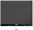
- the etching rate was also evaluated using the "Method for calculating etching rate of ruthenium" described above. From the calculated etching rate, the time required to etch 50 ⁇ ⁇ 10 ⁇ of ruthenium was calculated, and a ruthenium film treated for the time required to etch 50 ⁇ ⁇ 10 ⁇ was prepared, and used as the ruthenium film for surface observation. The ruthenium surface was observed using an electron microscope of 100000x power. The results of the observation are shown in FIG. 3 .
- aqueous solution of tetramethylammonium hypochlorite was obtained identically with Experimental Example 1-1, except that the amount of the ion exchange resin in the step (a) was set at 564 mL, the feed amount of the 10% tetramethylammonium hydroxide solution was set at 2 L, and the concentration of the aqueous solution of sodium hypochlorite in the step (b) was set at 8.39 mass%.
- TMAH tetramethylammonium hydroxide
- aqueous solution of tetramethylammonium hypochlorite was obtained identically with Example 1, except that the amount of the ion exchange resin in the step (a) was set at 705 mL, the feed amount of the 10% tetramethylammonium hydroxide solution was set at 2 L, and the concentration of the aqueous solution of sodium hypochlorite in the step (b) was set at 10.49 mass%.
- TMAH tetramethylammonium hydroxide
- aqueous solution of tetramethylammonium hypochlorite was obtained identically with Experimental Example 1-1, except that the amount of the ion exchange resin in the step (a) was set at 282 mL, and the concentration of the aqueous solution of sodium hypochlorite in the step (b) was set at 4.20 mass%.
- TMAH tetramethylammonium hydroxide
- the amount of ion exchange resin in the step (a) was set at 282 mL, and the concentration of the aqueous solution of sodium hypochlorite in the step (b) was set at 4.20 mass%.
- 500 mg of didecyldimethylammonium chloride was added to obtain a treatment liquid having the composition registered in Table 1. The evaluation results are shown in Table 2.
- a treatment liquid was prepared in the same manner as in Experimental Example 1-1, except that the alkylammonium salt expressed by Formula (1) was not added, and the same evaluation as in Experimental Example 1-1 was performed.
- FIG. 3 shows an electron microscopic image of 100000x of the ruthenium after the etching treatment obtained in Experimental Example 1-1. It is to be known that formation of RuO 2 (particles) on the wafer surface was inhibited and a flat ruthenium surface was obtained.
Landscapes
- Chemical & Material Sciences (AREA)
- Organic Chemistry (AREA)
- Engineering & Computer Science (AREA)
- Materials Engineering (AREA)
- Chemical Kinetics & Catalysis (AREA)
- General Chemical & Material Sciences (AREA)
- Mechanical Engineering (AREA)
- Metallurgy (AREA)
- Inorganic Chemistry (AREA)
- Health & Medical Sciences (AREA)
- Biochemistry (AREA)
- General Health & Medical Sciences (AREA)
- Molecular Biology (AREA)
- Life Sciences & Earth Sciences (AREA)
- Cleaning Or Drying Semiconductors (AREA)
- ing And Chemical Polishing (AREA)
- Weting (AREA)
- Organic Low-Molecular-Weight Compounds And Preparation Thereof (AREA)
Applications Claiming Priority (5)
| Application Number | Priority Date | Filing Date | Title |
|---|---|---|---|
| JP2019024016 | 2019-02-13 | ||
| JP2019045761 | 2019-03-13 | ||
| JP2019093194 | 2019-05-16 | ||
| JP2019110984 | 2019-06-14 | ||
| PCT/JP2020/005663 WO2020166677A1 (ja) | 2019-02-13 | 2020-02-13 | オニウム塩を含む半導体ウェハの処理液 |
Publications (3)
| Publication Number | Publication Date |
|---|---|
| EP3926662A1 EP3926662A1 (en) | 2021-12-22 |
| EP3926662A4 EP3926662A4 (en) | 2023-01-11 |
| EP3926662B1 true EP3926662B1 (en) | 2025-04-30 |
Family
ID=72044225
Family Applications (1)
| Application Number | Title | Priority Date | Filing Date |
|---|---|---|---|
| EP20756178.8A Active EP3926662B1 (en) | 2019-02-13 | 2020-02-13 | Onium salt-containing processing solution for semiconductor wafers |
Country Status (8)
| Country | Link |
|---|---|
| US (1) | US12024663B2 (https=) |
| EP (1) | EP3926662B1 (https=) |
| JP (1) | JP7477466B2 (https=) |
| KR (1) | KR102820838B1 (https=) |
| CN (1) | CN113383408B (https=) |
| SG (1) | SG11202108772PA (https=) |
| TW (1) | TWI904082B (https=) |
| WO (1) | WO2020166677A1 (https=) |
Families Citing this family (8)
| Publication number | Priority date | Publication date | Assignee | Title |
|---|---|---|---|---|
| WO2020256007A1 (ja) * | 2019-06-21 | 2020-12-24 | 株式会社トクヤマ | 酸化ルテニウムガスの吸収液、酸化ルテニウムの分析方法およびトラップ装置、定量分析装置 |
| WO2021210308A1 (ja) * | 2020-04-16 | 2021-10-21 | 富士フイルムエレクトロニクスマテリアルズ株式会社 | 洗浄液、洗浄方法 |
| WO2021210310A1 (ja) * | 2020-04-16 | 2021-10-21 | 富士フイルムエレクトロニクスマテリアルズ株式会社 | 処理液、化学的機械的研磨方法、半導体基板の処理方法 |
| WO2022050273A1 (ja) * | 2020-09-03 | 2022-03-10 | 富士フイルム株式会社 | 組成物、基板の処理方法 |
| JP7819114B2 (ja) * | 2020-11-26 | 2026-02-24 | 株式会社トクヤマ | 半導体ウェハの処理液及びその製造方法 |
| WO2022138561A1 (ja) * | 2020-12-25 | 2022-06-30 | 株式会社トクヤマ | 遷移金属を含む半導体の処理方法、遷移金属を含む半導体の製造方法、および半導体用処理液 |
| JPWO2023190984A1 (https=) * | 2022-03-31 | 2023-10-05 | ||
| JP7809031B2 (ja) * | 2022-08-22 | 2026-01-30 | 株式会社Screenホールディングス | 基板処理方法および基板処理装置 |
Family Cites Families (33)
| Publication number | Priority date | Publication date | Assignee | Title |
|---|---|---|---|---|
| JPS5314019B2 (https=) | 1972-12-20 | 1978-05-15 | ||
| JPS5650112Y2 (https=) | 1976-07-16 | 1981-11-24 | ||
| JP3690837B2 (ja) * | 1995-05-02 | 2005-08-31 | 株式会社荏原製作所 | ポリッシング装置及び方法 |
| US6143192A (en) | 1998-09-03 | 2000-11-07 | Micron Technology, Inc. | Ruthenium and ruthenium dioxide removal method and material |
| TW490756B (en) | 1999-08-31 | 2002-06-11 | Hitachi Ltd | Method for mass production of semiconductor integrated circuit device and manufacturing method of electronic components |
| JP4510979B2 (ja) | 2000-02-23 | 2010-07-28 | ルネサスエレクトロニクス株式会社 | ルテニウム又は酸化ルテニウム除去液の使用方法、及びルテニウム又は酸化ルテニウムの除去方法 |
| JP3585437B2 (ja) * | 2000-11-22 | 2004-11-04 | 株式会社荏原製作所 | ルテニウム膜のエッチング方法 |
| US6498110B2 (en) * | 2001-03-05 | 2002-12-24 | Micron Technology, Inc. | Ruthenium silicide wet etch |
| JP4043234B2 (ja) | 2001-06-18 | 2008-02-06 | 株式会社荏原製作所 | 電解加工装置及び基板処理装置 |
| JP3833139B2 (ja) * | 2002-04-26 | 2006-10-11 | 株式会社荏原製作所 | 電解加工装置 |
| WO2006087099A1 (en) * | 2005-02-16 | 2006-08-24 | Unilever N.V. | Aqueous liquid bleach compositions |
| WO2006110279A1 (en) * | 2005-04-08 | 2006-10-19 | Sachem, Inc. | Selective wet etching of metal nitrides |
| US20090212021A1 (en) * | 2005-06-13 | 2009-08-27 | Advanced Technology Materials, Inc. | Compositions and methods for selective removal of metal or metal alloy after metal silicide formation |
| KR100827591B1 (ko) * | 2006-11-27 | 2008-05-07 | 제일모직주식회사 | 화학적 기계적 연마용 슬러리 조성물 및 그 전구체 조성물 |
| WO2008129891A1 (ja) | 2007-04-13 | 2008-10-30 | Tosoh Corporation | エッチング用組成物及びエッチング方法 |
| JP4552968B2 (ja) * | 2007-05-29 | 2010-09-29 | 住友電気工業株式会社 | 化合物半導体基板の研磨方法、化合物半導体基板、化合物半導体エピ基板の製造方法および化合物半導体エピ基板 |
| US8008202B2 (en) | 2007-08-01 | 2011-08-30 | Cabot Microelectronics Corporation | Ruthenium CMP compositions and methods |
| CN101802911B (zh) * | 2007-09-14 | 2013-01-02 | 花王株式会社 | 用于垂直磁记录方式硬盘用基板的水系洗涤剂组合物 |
| KR100980607B1 (ko) * | 2007-11-08 | 2010-09-07 | 주식회사 하이닉스반도체 | 루테늄 연마용 슬러리 및 그를 이용한 연마 방법 |
| JP4848402B2 (ja) * | 2008-08-20 | 2011-12-28 | ルネサスエレクトロニクス株式会社 | 半導体集積回路装置の製造方法 |
| WO2011074601A1 (ja) * | 2009-12-17 | 2011-06-23 | 昭和電工株式会社 | ルテニウム系金属のエッチング用組成物およびその調製方法 |
| WO2013099955A1 (ja) * | 2011-12-27 | 2013-07-04 | 富士フイルム株式会社 | 半導体基板製品の製造方法及びこれに利用されるエッチング方法 |
| US10472567B2 (en) | 2013-03-04 | 2019-11-12 | Entegris, Inc. | Compositions and methods for selectively etching titanium nitride |
| WO2016068183A1 (ja) * | 2014-10-31 | 2016-05-06 | 富士フイルム株式会社 | ルテニウム除去組成物、及び、磁気抵抗メモリの製造方法 |
| TWI654288B (zh) * | 2015-01-12 | 2019-03-21 | 美商慧盛材料美國責任有限公司 | 用於化學機械平坦化組合物之複合硏磨粒及其使用方法 |
| WO2016140246A1 (ja) * | 2015-03-04 | 2016-09-09 | 日立化成株式会社 | Cmp用研磨液、及び、これを用いた研磨方法 |
| JP6747432B2 (ja) * | 2015-04-13 | 2020-08-26 | 三菱瓦斯化学株式会社 | ウェハを再生するための炭素含有シリコン酸化物を含む材料の洗浄液および洗浄方法 |
| US9976111B2 (en) | 2015-05-01 | 2018-05-22 | Versum Materials Us, Llc | TiN hard mask and etch residual removal |
| JP6761166B2 (ja) | 2015-07-23 | 2020-09-23 | セントラル硝子株式会社 | ウェットエッチング方法及びエッチング液 |
| JP6966570B2 (ja) * | 2017-04-11 | 2021-11-17 | インテグリス・インコーポレーテッド | 化学機械研磨後配合物及び使用方法 |
| CN107976354A (zh) * | 2017-11-22 | 2018-05-01 | 中山市创艺生化工程有限公司 | 一种血细胞分析仪用试剂 |
| JP7219061B2 (ja) | 2018-11-14 | 2023-02-07 | 関東化学株式会社 | ルテニウム除去用組成物 |
| US11346008B2 (en) | 2018-12-14 | 2022-05-31 | Entegris, Inc. | Ruthenium etching composition and method |
-
2020
- 2020-02-13 WO PCT/JP2020/005663 patent/WO2020166677A1/ja not_active Ceased
- 2020-02-13 SG SG11202108772PA patent/SG11202108772PA/en unknown
- 2020-02-13 KR KR1020217022555A patent/KR102820838B1/ko active Active
- 2020-02-13 TW TW109104611A patent/TWI904082B/zh active
- 2020-02-13 US US17/419,058 patent/US12024663B2/en active Active
- 2020-02-13 EP EP20756178.8A patent/EP3926662B1/en active Active
- 2020-02-13 CN CN202080012317.0A patent/CN113383408B/zh active Active
- 2020-02-13 JP JP2020572319A patent/JP7477466B2/ja active Active
Also Published As
| Publication number | Publication date |
|---|---|
| SG11202108772PA (en) | 2021-09-29 |
| JP7477466B2 (ja) | 2024-05-01 |
| KR102820838B1 (ko) | 2025-06-13 |
| KR20210127920A (ko) | 2021-10-25 |
| US12024663B2 (en) | 2024-07-02 |
| TWI904082B (zh) | 2025-11-11 |
| CN113383408B (zh) | 2025-04-08 |
| CN113383408A (zh) | 2021-09-10 |
| JPWO2020166677A1 (https=) | 2020-08-20 |
| WO2020166677A1 (ja) | 2020-08-20 |
| US20220073820A1 (en) | 2022-03-10 |
| EP3926662A4 (en) | 2023-01-11 |
| TW202035355A (zh) | 2020-10-01 |
| EP3926662A1 (en) | 2021-12-22 |
Similar Documents
| Publication | Publication Date | Title |
|---|---|---|
| EP3926662B1 (en) | Onium salt-containing processing solution for semiconductor wafers | |
| TWI899006B (zh) | 含有次氯酸離子的半導體晶圓處理液 | |
| US11932590B2 (en) | Inhibitor for RuO4 gas generation and method for inhibiting RuO4 gas generation | |
| JP5037442B2 (ja) | 窒化チタン除去液、窒化チタン被膜の除去方法、及び窒化チタン除去液の製造方法 | |
| WO2022030627A1 (ja) | 半導体ウエハ用処理液 | |
| EP3926663A1 (en) | Semiconductor wafer treatment liquid containing hypochlorite ions and ph buffer | |
| US12444617B2 (en) | Semiconductor wafer processing liquid containing hypobromite ions and PH buffering agent | |
| WO2022114036A1 (ja) | 半導体ウェハの処理液及びその製造方法 | |
| CN116235282A (zh) | 半导体基板清洗用组合物和清洗方法 | |
| JP7081010B2 (ja) | オニウム塩を含む半導体ウェハの処理液 |
Legal Events
| Date | Code | Title | Description |
|---|---|---|---|
| STAA | Information on the status of an ep patent application or granted ep patent |
Free format text: STATUS: THE INTERNATIONAL PUBLICATION HAS BEEN MADE |
|
| PUAI | Public reference made under article 153(3) epc to a published international application that has entered the european phase |
Free format text: ORIGINAL CODE: 0009012 |
|
| STAA | Information on the status of an ep patent application or granted ep patent |
Free format text: STATUS: REQUEST FOR EXAMINATION WAS MADE |
|
| 17P | Request for examination filed |
Effective date: 20210902 |
|
| AK | Designated contracting states |
Kind code of ref document: A1 Designated state(s): AL AT BE BG CH CY CZ DE DK EE ES FI FR GB GR HR HU IE IS IT LI LT LU LV MC MK MT NL NO PL PT RO RS SE SI SK SM TR |
|
| DAV | Request for validation of the european patent (deleted) | ||
| DAX | Request for extension of the european patent (deleted) | ||
| RIC1 | Information provided on ipc code assigned before grant |
Ipc: C23F 1/46 20060101ALI20220913BHEP Ipc: C23F 1/40 20060101ALI20220913BHEP Ipc: C09K 13/06 20060101ALI20220913BHEP Ipc: C09K 13/04 20060101ALI20220913BHEP Ipc: C07F 9/54 20060101ALI20220913BHEP Ipc: C07C 381/12 20060101ALI20220913BHEP Ipc: C07C 211/63 20060101ALI20220913BHEP Ipc: H01L 23/532 20060101ALI20220913BHEP Ipc: H01L 21/768 20060101ALI20220913BHEP Ipc: H01L 21/3213 20060101AFI20220913BHEP |
|
| REG | Reference to a national code |
Ref legal event code: R079 Ipc: H01L0021321300 Ref country code: DE Ref document number: 602020050427 Country of ref document: DE Free format text: PREVIOUS MAIN CLASS: H01L0021306000 |
|
| A4 | Supplementary search report drawn up and despatched |
Effective date: 20221209 |
|
| RIC1 | Information provided on ipc code assigned before grant |
Ipc: C09K 13/00 20060101ALI20221205BHEP Ipc: C07F 9/54 20060101ALI20221205BHEP Ipc: C07C 381/12 20060101ALI20221205BHEP Ipc: C07C 211/63 20060101ALI20221205BHEP Ipc: C23F 1/46 20060101ALI20221205BHEP Ipc: C23F 1/40 20060101ALI20221205BHEP Ipc: H01L 23/532 20060101ALI20221205BHEP Ipc: H01L 21/768 20060101ALI20221205BHEP Ipc: H01L 21/3213 20060101AFI20221205BHEP |
|
| GRAP | Despatch of communication of intention to grant a patent |
Free format text: ORIGINAL CODE: EPIDOSNIGR1 |
|
| STAA | Information on the status of an ep patent application or granted ep patent |
Free format text: STATUS: GRANT OF PATENT IS INTENDED |
|
| INTG | Intention to grant announced |
Effective date: 20241206 |
|
| GRAS | Grant fee paid |
Free format text: ORIGINAL CODE: EPIDOSNIGR3 |
|
| GRAA | (expected) grant |
Free format text: ORIGINAL CODE: 0009210 |
|
| STAA | Information on the status of an ep patent application or granted ep patent |
Free format text: STATUS: THE PATENT HAS BEEN GRANTED |
|
| AK | Designated contracting states |
Kind code of ref document: B1 Designated state(s): AL AT BE BG CH CY CZ DE DK EE ES FI FR GB GR HR HU IE IS IT LI LT LU LV MC MK MT NL NO PL PT RO RS SE SI SK SM TR |
|
| REG | Reference to a national code |
Ref country code: CH Ref legal event code: EP Ref country code: GB Ref legal event code: FG4D |
|
| REG | Reference to a national code |
Ref country code: DE Ref legal event code: R096 Ref document number: 602020050427 Country of ref document: DE |
|
| REG | Reference to a national code |
Ref country code: IE Ref legal event code: FG4D |
|
| REG | Reference to a national code |
Ref country code: NL Ref legal event code: FP |
|
| REG | Reference to a national code |
Ref country code: AT Ref legal event code: MK05 Ref document number: 1790887 Country of ref document: AT Kind code of ref document: T Effective date: 20250430 |
|
| PG25 | Lapsed in a contracting state [announced via postgrant information from national office to epo] |
Ref country code: FI Free format text: LAPSE BECAUSE OF FAILURE TO SUBMIT A TRANSLATION OF THE DESCRIPTION OR TO PAY THE FEE WITHIN THE PRESCRIBED TIME-LIMIT Effective date: 20250430 Ref country code: ES Free format text: LAPSE BECAUSE OF FAILURE TO SUBMIT A TRANSLATION OF THE DESCRIPTION OR TO PAY THE FEE WITHIN THE PRESCRIBED TIME-LIMIT Effective date: 20250430 Ref country code: PT Free format text: LAPSE BECAUSE OF FAILURE TO SUBMIT A TRANSLATION OF THE DESCRIPTION OR TO PAY THE FEE WITHIN THE PRESCRIBED TIME-LIMIT Effective date: 20250901 |
|
| REG | Reference to a national code |
Ref country code: LT Ref legal event code: MG9D |
|
| PG25 | Lapsed in a contracting state [announced via postgrant information from national office to epo] |
Ref country code: GR Free format text: LAPSE BECAUSE OF FAILURE TO SUBMIT A TRANSLATION OF THE DESCRIPTION OR TO PAY THE FEE WITHIN THE PRESCRIBED TIME-LIMIT Effective date: 20250731 Ref country code: NO Free format text: LAPSE BECAUSE OF FAILURE TO SUBMIT A TRANSLATION OF THE DESCRIPTION OR TO PAY THE FEE WITHIN THE PRESCRIBED TIME-LIMIT Effective date: 20250730 |
|
| PG25 | Lapsed in a contracting state [announced via postgrant information from national office to epo] |
Ref country code: PL Free format text: LAPSE BECAUSE OF FAILURE TO SUBMIT A TRANSLATION OF THE DESCRIPTION OR TO PAY THE FEE WITHIN THE PRESCRIBED TIME-LIMIT Effective date: 20250430 |
|
| PG25 | Lapsed in a contracting state [announced via postgrant information from national office to epo] |
Ref country code: BG Free format text: LAPSE BECAUSE OF FAILURE TO SUBMIT A TRANSLATION OF THE DESCRIPTION OR TO PAY THE FEE WITHIN THE PRESCRIBED TIME-LIMIT Effective date: 20250430 |
|
| PG25 | Lapsed in a contracting state [announced via postgrant information from national office to epo] |
Ref country code: HR Free format text: LAPSE BECAUSE OF FAILURE TO SUBMIT A TRANSLATION OF THE DESCRIPTION OR TO PAY THE FEE WITHIN THE PRESCRIBED TIME-LIMIT Effective date: 20250430 |
|
| PG25 | Lapsed in a contracting state [announced via postgrant information from national office to epo] |
Ref country code: AT Free format text: LAPSE BECAUSE OF FAILURE TO SUBMIT A TRANSLATION OF THE DESCRIPTION OR TO PAY THE FEE WITHIN THE PRESCRIBED TIME-LIMIT Effective date: 20250430 |
|
| PG25 | Lapsed in a contracting state [announced via postgrant information from national office to epo] |
Ref country code: RS Free format text: LAPSE BECAUSE OF FAILURE TO SUBMIT A TRANSLATION OF THE DESCRIPTION OR TO PAY THE FEE WITHIN THE PRESCRIBED TIME-LIMIT Effective date: 20250731 |
|
| PG25 | Lapsed in a contracting state [announced via postgrant information from national office to epo] |
Ref country code: IS Free format text: LAPSE BECAUSE OF FAILURE TO SUBMIT A TRANSLATION OF THE DESCRIPTION OR TO PAY THE FEE WITHIN THE PRESCRIBED TIME-LIMIT Effective date: 20250830 |
|
| PG25 | Lapsed in a contracting state [announced via postgrant information from national office to epo] |
Ref country code: LV Free format text: LAPSE BECAUSE OF FAILURE TO SUBMIT A TRANSLATION OF THE DESCRIPTION OR TO PAY THE FEE WITHIN THE PRESCRIBED TIME-LIMIT Effective date: 20250430 |
|
| REG | Reference to a national code |
Ref country code: DE Ref legal event code: R079 Ref document number: 602020050427 Country of ref document: DE Free format text: PREVIOUS MAIN CLASS: H01L0021321300 Ipc: H10P0050260000 |
|
| PG25 | Lapsed in a contracting state [announced via postgrant information from national office to epo] |
Ref country code: DK Free format text: LAPSE BECAUSE OF FAILURE TO SUBMIT A TRANSLATION OF THE DESCRIPTION OR TO PAY THE FEE WITHIN THE PRESCRIBED TIME-LIMIT Effective date: 20250430 Ref country code: SM Free format text: LAPSE BECAUSE OF FAILURE TO SUBMIT A TRANSLATION OF THE DESCRIPTION OR TO PAY THE FEE WITHIN THE PRESCRIBED TIME-LIMIT Effective date: 20250430 |
|
| PG25 | Lapsed in a contracting state [announced via postgrant information from national office to epo] |
Ref country code: CZ Free format text: LAPSE BECAUSE OF FAILURE TO SUBMIT A TRANSLATION OF THE DESCRIPTION OR TO PAY THE FEE WITHIN THE PRESCRIBED TIME-LIMIT Effective date: 20250430 |
|
| PG25 | Lapsed in a contracting state [announced via postgrant information from national office to epo] |
Ref country code: EE Free format text: LAPSE BECAUSE OF FAILURE TO SUBMIT A TRANSLATION OF THE DESCRIPTION OR TO PAY THE FEE WITHIN THE PRESCRIBED TIME-LIMIT Effective date: 20250430 |
|
| PG25 | Lapsed in a contracting state [announced via postgrant information from national office to epo] |
Ref country code: RO Free format text: LAPSE BECAUSE OF FAILURE TO SUBMIT A TRANSLATION OF THE DESCRIPTION OR TO PAY THE FEE WITHIN THE PRESCRIBED TIME-LIMIT Effective date: 20250430 Ref country code: SK Free format text: LAPSE BECAUSE OF FAILURE TO SUBMIT A TRANSLATION OF THE DESCRIPTION OR TO PAY THE FEE WITHIN THE PRESCRIBED TIME-LIMIT Effective date: 20250430 |
|
| PG25 | Lapsed in a contracting state [announced via postgrant information from national office to epo] |
Ref country code: IT Free format text: LAPSE BECAUSE OF FAILURE TO SUBMIT A TRANSLATION OF THE DESCRIPTION OR TO PAY THE FEE WITHIN THE PRESCRIBED TIME-LIMIT Effective date: 20250430 |
|
| REG | Reference to a national code |
Ref country code: DE Ref legal event code: R097 Ref document number: 602020050427 Country of ref document: DE |
|
| PLBE | No opposition filed within time limit |
Free format text: ORIGINAL CODE: 0009261 |
|
| STAA | Information on the status of an ep patent application or granted ep patent |
Free format text: STATUS: NO OPPOSITION FILED WITHIN TIME LIMIT |
|
| REG | Reference to a national code |
Ref country code: CH Ref legal event code: L10 Free format text: ST27 STATUS EVENT CODE: U-0-0-L10-L00 (AS PROVIDED BY THE NATIONAL OFFICE) Effective date: 20260311 |
|
| PGFP | Annual fee paid to national office [announced via postgrant information from national office to epo] |
Ref country code: NL Payment date: 20260218 Year of fee payment: 7 |
|
| 26N | No opposition filed |
Effective date: 20260202 |
|
| PGFP | Annual fee paid to national office [announced via postgrant information from national office to epo] |
Ref country code: DE Payment date: 20260218 Year of fee payment: 7 |
|
| PGFP | Annual fee paid to national office [announced via postgrant information from national office to epo] |
Ref country code: BE Payment date: 20260218 Year of fee payment: 7 |