EP3915147B1 - Neuartige 3d-nand-speichervorrichtung und verfahren zu ihrer herstellung - Google Patents
Neuartige 3d-nand-speichervorrichtung und verfahren zu ihrer herstellung Download PDFInfo
- Publication number
- EP3915147B1 EP3915147B1 EP19935559.5A EP19935559A EP3915147B1 EP 3915147 B1 EP3915147 B1 EP 3915147B1 EP 19935559 A EP19935559 A EP 19935559A EP 3915147 B1 EP3915147 B1 EP 3915147B1
- Authority
- EP
- European Patent Office
- Prior art keywords
- substrate
- coupled
- connection structure
- doped region
- forming
- Prior art date
- Legal status (The legal status is an assumption and is not a legal conclusion. Google has not performed a legal analysis and makes no representation as to the accuracy of the status listed.)
- Active
Links
Images


Classifications
-
- H—ELECTRICITY
- H10—SEMICONDUCTOR DEVICES; ELECTRIC SOLID-STATE DEVICES NOT OTHERWISE PROVIDED FOR
- H10B—ELECTRONIC MEMORY DEVICES
- H10B43/00—EEPROM devices comprising charge-trapping gate insulators
- H10B43/50—EEPROM devices comprising charge-trapping gate insulators characterised by the boundary region between the core and peripheral circuit regions
-
- H—ELECTRICITY
- H10—SEMICONDUCTOR DEVICES; ELECTRIC SOLID-STATE DEVICES NOT OTHERWISE PROVIDED FOR
- H10B—ELECTRONIC MEMORY DEVICES
- H10B41/00—Electrically erasable-and-programmable ROM [EEPROM] devices comprising floating gates
- H10B41/20—Electrically erasable-and-programmable ROM [EEPROM] devices comprising floating gates characterised by three-dimensional [3D] arrangements, e.g. with cells on different height levels
- H10B41/23—Electrically erasable-and-programmable ROM [EEPROM] devices comprising floating gates characterised by three-dimensional [3D] arrangements, e.g. with cells on different height levels with source and drain on different levels, e.g. with sloping channels
- H10B41/27—Electrically erasable-and-programmable ROM [EEPROM] devices comprising floating gates characterised by three-dimensional [3D] arrangements, e.g. with cells on different height levels with source and drain on different levels, e.g. with sloping channels the channels comprising vertical portions, e.g. U-shaped channels
-
- H—ELECTRICITY
- H10—SEMICONDUCTOR DEVICES; ELECTRIC SOLID-STATE DEVICES NOT OTHERWISE PROVIDED FOR
- H10B—ELECTRONIC MEMORY DEVICES
- H10B41/00—Electrically erasable-and-programmable ROM [EEPROM] devices comprising floating gates
- H10B41/30—Electrically erasable-and-programmable ROM [EEPROM] devices comprising floating gates characterised by the memory core region
- H10B41/35—Electrically erasable-and-programmable ROM [EEPROM] devices comprising floating gates characterised by the memory core region with a cell select transistor, e.g. NAND
-
- H—ELECTRICITY
- H10—SEMICONDUCTOR DEVICES; ELECTRIC SOLID-STATE DEVICES NOT OTHERWISE PROVIDED FOR
- H10B—ELECTRONIC MEMORY DEVICES
- H10B41/00—Electrically erasable-and-programmable ROM [EEPROM] devices comprising floating gates
- H10B41/40—Electrically erasable-and-programmable ROM [EEPROM] devices comprising floating gates characterised by the peripheral circuit region
- H10B41/41—Electrically erasable-and-programmable ROM [EEPROM] devices comprising floating gates characterised by the peripheral circuit region of a memory region comprising a cell select transistor, e.g. NAND
-
- H—ELECTRICITY
- H10—SEMICONDUCTOR DEVICES; ELECTRIC SOLID-STATE DEVICES NOT OTHERWISE PROVIDED FOR
- H10B—ELECTRONIC MEMORY DEVICES
- H10B43/00—EEPROM devices comprising charge-trapping gate insulators
- H10B43/20—EEPROM devices comprising charge-trapping gate insulators characterised by three-dimensional [3D] arrangements, e.g. with cells on different height levels
- H10B43/23—EEPROM devices comprising charge-trapping gate insulators characterised by three-dimensional [3D] arrangements, e.g. with cells on different height levels with source and drain on different levels, e.g. with sloping channels
- H10B43/27—EEPROM devices comprising charge-trapping gate insulators characterised by three-dimensional [3D] arrangements, e.g. with cells on different height levels with source and drain on different levels, e.g. with sloping channels the channels comprising vertical portions, e.g. U-shaped channels
-
- H—ELECTRICITY
- H10—SEMICONDUCTOR DEVICES; ELECTRIC SOLID-STATE DEVICES NOT OTHERWISE PROVIDED FOR
- H10B—ELECTRONIC MEMORY DEVICES
- H10B43/00—EEPROM devices comprising charge-trapping gate insulators
- H10B43/30—EEPROM devices comprising charge-trapping gate insulators characterised by the memory core region
- H10B43/35—EEPROM devices comprising charge-trapping gate insulators characterised by the memory core region with cell select transistors, e.g. NAND
-
- H—ELECTRICITY
- H10—SEMICONDUCTOR DEVICES; ELECTRIC SOLID-STATE DEVICES NOT OTHERWISE PROVIDED FOR
- H10B—ELECTRONIC MEMORY DEVICES
- H10B43/00—EEPROM devices comprising charge-trapping gate insulators
- H10B43/40—EEPROM devices comprising charge-trapping gate insulators characterised by the peripheral circuit region
-
- H—ELECTRICITY
- H10—SEMICONDUCTOR DEVICES; ELECTRIC SOLID-STATE DEVICES NOT OTHERWISE PROVIDED FOR
- H10D—INORGANIC ELECTRIC SEMICONDUCTOR DEVICES
- H10D84/00—Integrated devices formed in or on semiconductor substrates that comprise only semiconducting layers, e.g. on Si wafers or on GaAs-on-Si wafers
- H10D84/01—Manufacture or treatment
- H10D84/0123—Integrating together multiple components covered by H10D12/00 or H10D30/00, e.g. integrating multiple IGBTs
- H10D84/0126—Integrating together multiple components covered by H10D12/00 or H10D30/00, e.g. integrating multiple IGBTs the components including insulated gates, e.g. IGFETs
- H10D84/0149—Manufacturing their interconnections or electrodes, e.g. source or drain electrodes
-
- H—ELECTRICITY
- H10—SEMICONDUCTOR DEVICES; ELECTRIC SOLID-STATE DEVICES NOT OTHERWISE PROVIDED FOR
- H10P—GENERIC PROCESSES OR APPARATUS FOR THE MANUFACTURE OR TREATMENT OF DEVICES COVERED BY CLASS H10
- H10P50/00—Etching of wafers, substrates or parts of devices
- H10P50/73—Etching of wafers, substrates or parts of devices using masks for insulating materials
-
- H—ELECTRICITY
- H10—SEMICONDUCTOR DEVICES; ELECTRIC SOLID-STATE DEVICES NOT OTHERWISE PROVIDED FOR
- H10W—GENERIC PACKAGES, INTERCONNECTIONS, CONNECTORS OR OTHER CONSTRUCTIONAL DETAILS OF DEVICES COVERED BY CLASS H10
- H10W20/00—Interconnections in chips, wafers or substrates
- H10W20/20—Interconnections within wafers or substrates, e.g. through-silicon vias [TSV]
-
- H—ELECTRICITY
- H10—SEMICONDUCTOR DEVICES; ELECTRIC SOLID-STATE DEVICES NOT OTHERWISE PROVIDED FOR
- H10W—GENERIC PACKAGES, INTERCONNECTIONS, CONNECTORS OR OTHER CONSTRUCTIONAL DETAILS OF DEVICES COVERED BY CLASS H10
- H10W72/00—Interconnections or connectors in packages
- H10W72/01—Manufacture or treatment
- H10W72/0198—Manufacture or treatment batch processes
-
- H—ELECTRICITY
- H10—SEMICONDUCTOR DEVICES; ELECTRIC SOLID-STATE DEVICES NOT OTHERWISE PROVIDED FOR
- H10W—GENERIC PACKAGES, INTERCONNECTIONS, CONNECTORS OR OTHER CONSTRUCTIONAL DETAILS OF DEVICES COVERED BY CLASS H10
- H10W80/00—Direct bonding of chips, wafers or substrates
- H10W80/301—Bonding techniques, e.g. hybrid bonding
- H10W80/312—Bonding techniques, e.g. hybrid bonding characterised by the direct bonding of electrically conductive pads
-
- H—ELECTRICITY
- H10—SEMICONDUCTOR DEVICES; ELECTRIC SOLID-STATE DEVICES NOT OTHERWISE PROVIDED FOR
- H10W—GENERIC PACKAGES, INTERCONNECTIONS, CONNECTORS OR OTHER CONSTRUCTIONAL DETAILS OF DEVICES COVERED BY CLASS H10
- H10W80/00—Direct bonding of chips, wafers or substrates
- H10W80/301—Bonding techniques, e.g. hybrid bonding
- H10W80/327—Bonding techniques, e.g. hybrid bonding characterised by the direct bonding of insulating parts, e.g. of silicon oxide layers
-
- H—ELECTRICITY
- H10—SEMICONDUCTOR DEVICES; ELECTRIC SOLID-STATE DEVICES NOT OTHERWISE PROVIDED FOR
- H10W—GENERIC PACKAGES, INTERCONNECTIONS, CONNECTORS OR OTHER CONSTRUCTIONAL DETAILS OF DEVICES COVERED BY CLASS H10
- H10W90/00—Package configurations
- H10W90/701—Package configurations characterised by the relative positions of pads or connectors relative to package parts
- H10W90/791—Package configurations characterised by the relative positions of pads or connectors relative to package parts of direct-bonded pads
- H10W90/792—Package configurations characterised by the relative positions of pads or connectors relative to package parts of direct-bonded pads between multiple chips
Definitions
- a 3D-NAND memory device is an exemplary device of stacking multiple planes of memory cells to achieve greater storage capacity, and to achieve lower costs per bit.
- periphery circuits take up about 20-30% of die area, which lowers NAND bit density. As 3D NAND technology continues to progress to 128 layers and above, the periphery circuits will likely take up more than 50% of the total die area.
- CMOS wafer complementary metal-oxide-semiconductor
- logic technology node i.e. 14nm, 7nm
- VOAs metal vertical interconnect accesses
- US 2018 / 0 277 517 A1 discloses a semiconductor device.
- WO 2020 / 0 211 332 A1 discloses a stacked three-dimensional heterogeneous memory devices and methods for forming same.
- US 2019 / 0 081 069 A1 discloses a three-dimensional memory devices and methods for forming the same.
- inventive concepts relate to formation of a 3D NAND memory device according to claim 1.
- Another aspect relates to a method for manufacturing a 3D-NAND memory device according to claim 7.
- a related 3D-NAND memory device can include two or more n-well regions formed in a top region of a substrate, and two or more array common source (ACS) structures that are formed over the two or more n-well regions. Each of the two or more ACS structures is in contact with a respective n-well region.
- the related 3D-NAND memory device can also have a plurality of M1 routing lines. The M1 routing lines are electrically coupled to the ACS structures through a plurality of M1 VIAs. A plurality of source lines are positioned over the plurality of M2 routing lines. The source lines are electrically coupled to the M1 routing lines through a plurality of M2 VIAs.
- an input voltage is applied to the n-well regions through a conductive channel that is formed by the source lines, the M2 VIAs, the M1 routing lines, the M1 VIAs, and the ACS structures.
- the ACS structures typically are wall-shaped line contacts along a word line (WL) direction of the 3D-NAND memory device. Such a wall-shaped contact needs sufficient conductivity to prevent a ground noise from arising in sensing operations.
- the ACS structures can be formed with tungsten, polysilicon, or tungsten plus polysilicon because tungsten, polysilicon, or tungsten plus polysilicon are appropriate materials to conformally fill deep and wide contact trenches with minimal voids.
- tungsten and polysilicon have relatively high resistivity compared to other contact metals, such as Cu or Al.
- a height of the ACS structures accordingly grows.
- a resistance of the ACS structures inevitably surges in a height direction of the 3D NAND stacks.
- a width of the ACS regions should get proportionally larger, which in turn impacts a die size and wafer mechanical stability due to high tungsten stress.
- a cross-stacking structure is applied to form a 3D-NAND memory device.
- a plurality of transistors are formed over the top surface of a CMOS substrate (or periphery circuit substrate), and a memory cell stack is formed over the top surface of a cell array substrate.
- the CMOS substrate is bonded through bonding VIAs with the cell array substrate.
- the top surface of the CMOS substrate and the top surface of the cell array substrate are aligned facing each other.
- two or more n-well regions extend in the cell array substrate from the top surface of the cell array substrate.
- a plurality of bottom source lines are formed over a bottom surface of the cell array wafer.
- the bottom source lines are coupled to the n-well regions through a plurality of VIA contacts.
- the VIA contacts are formed to extend from the bottom surface of the cell array wafer to reach the n-well regions.
- the n-well regions are coupled to a plurality of top source lines through a conductive channel that is formed by two or more ACS structures formed over and coupled to the n-well regions, a plurality of M1 routing lines formed over and coupled to the ACS structures, and a plurality of top source lines formed over and coupled to the M1 routing lines.
- the bottom source lines (or bottom source line mesh) can be electrically coupled to n-well regions from a polished backside (i.e., the bottom surface) of the cell array substrate. Accordingly, a resistance of source lines to n-well regions can be decreased.
- the present disclosure can have direct connection from source lines to n-well regions through VIA contacts made of conductive metal, such as Cu. In contrast to the related examples, the present disclosure can provide several advantages.
- the decreased resistance of source lines to n-well regions reduces ground noise that is a undesired voltage increase in the n-well regions.
- the resistance of the ACS structures does not impact a source side resistance of the memory device and the ground noise.
- the disclosed structure can eliminate gaps between M1 routing lines that are used to add contacts to connect source line mesh and ACS structures in the related examples, which in turn helps die size reduction in a word line direction.
- the semiconductor device includes a first substrate that has a first side for forming memory cells and a second side that is opposite to the first side.
- the semiconductor device also includes a doped region and a first connection structure (also referred to as a first source line mesh).
- the doped region is formed in the first side of the first substrate and is electrically coupled to at least a source terminal of a transistor (e.g., a source terminal of an end transistor of multiple transistors that are connected in series).
- the first connection structure is formed over the second side of the first substrate and coupled to the doped region through a first VIA.
- the first VIA extends from the second side of the first substrate to the doped region.
- the semiconductor device further includes a common source structure (also referred to as array common source structure) formed over and coupled to the doped region, a bit line formed over the common source structure that is coupled to the common source structure through a second VIA, and a second connection structure (also referred to as a second source line mesh) positioned over the bit line that is coupled to the bit line through a third VIA.
- the first connection structure and the second connection structure are coupled to each other.
- a transistor is formed in a first side of a second substrate and a bonding VIA formed over and coupled to the transistor.
- the first side of the first substrate and the first side of the second substrates are aligned facing each other so that the transistor is coupled to the second connection structure through the bonding VIA.
- the semiconductor device can further include a fourth VIA that is formed over the second connection structure and connected to the bonding VIA.
- the first substrate and the second substrate are bonded each other through the fourth VIA and the bonding VIA.
- the first VIA extends through the doped region and is in contact with the common source structure.
- the semiconductor device can include a spacer layer disposed between the first VIA and the first substrate so that isolates the first VIA from the first substrate.
- a highly doped n+ region can be arranged between the first VIA and the doped region, and the doped region is n-type.
- the first VIA can have at least one of an extended wall-shape that has a tapered cross section or a frustoconical shape.
- the semiconductor device further includes a plurality of channel structures extending from the first side of the first substrate, and a plurality of word lines positioned over the first side of the first substrate in a staircase configuration.
- the plurality of the word lines are spaced apart from each other by a plurality of insulating layers.
- the channel structures extend through the plurality of word lines and the plurality of the insulating layers.
- the plurality of channel structures are disposed below the bit line, and the common source structure extends through the plurality of word lines and the plurality of insulating layers and separates the plurality of the channel structures.
- a method for manufacturing a semiconductor device is disclosed.
- a first VIA that extends from a second side of the first substrate is formed.
- the first substrate has an opposing first side on which a memory stack is formed.
- the memory stack includes a doped region positioned in the first side of the first substrate.
- the doped region is electrically coupled to at least a source terminal of a transistor (e.g., a source terminal of an end transistor of multiple transistors that are connected in series) and the first VIA is in direct contact with the doped region.
- a first connection structure is formed over the first VIA so that the first connection structure is coupled to the doped region through the first VIA.
- a portion of first substrate is removed from the second side of the first substrate.
- the first VIA is subsequently formed.
- the first VIA extends from the second side of the first substrate to the doped region.
- the first connection structure is formed over the first VIA.
- a common source structure is formed over and coupled to the doped region.
- a bit line is formed over the common source structure, and the bit line is coupled to the common source structure through a second VIA.
- a second connection structure is formed over the bit line. The second connection structure is coupled to the bit line through a third VIA. The first connection structure and the second connection structure are coupled to each other.
- a transistor is formed over a first side of a second substrate.
- a bonding VIA is formed over the transistor.
- the bonding VIA is electrically coupled to the transistor.
- the first substrate and the second substrate are bonded through the bonding VIA, where the second connection structure is aligned with the transistor, and coupled to the transistor through the bonding VIA.
- a Through Silicon Via (TSV) is formed that extends from the second side of the first substrate to the first side of the first substrate.
- the first connection structure and the second connection structure are electrically connected through the TSV.
- a n+ region is formed between the first VIA and the doped region, and the doped region is n-type.
- the present invention provides for a 3D-NAND memory and its manufacturing method.
- the 3D-NAND memory includes a transistor formed in a first side of a periphery circuit substrate, a memory cell stack formed over a first side of a cell array substrate, and a first connection structure formed over an opposing second side of the cell array substrate.
- the memory cell stack further includes a doped region formed in the first side of the cell array substrate. The doped region is coupled to the first connection structure through the first VIA that extends from the second side of the cell array substrate to the doped region.
- the memory cell stack also includes a common source structure that extends from the doped region toward the first side of the periphery circuit substrate and is coupled to the doped region.
- a bit line is positioned between the common source structure and a second connection structure.
- the bit line is coupled to the common source structure through a second VIA.
- the second connection structure is coupled to the bit line through a third VIA, and the first side of the cell array substrate and the first side of a periphery circuit substrate are aligned facing each other so that the transistor is coupled to the second connection structure.
- first and second features are in direct contact with each other
- additional features are disposed formed between the first and second features, such that the first and second features may not be in direct contact
- present disclosure may repeat reference numerals and/or letters in the various examples. This repetition is for the purpose of simplicity and clarity and does not in itself dictate a relationship between the various embodiments and/or configurations discussed.
- spatially relative terms such as “beneath,” “below,” “lower,” “above,” “upper” and the like, may be used herein for ease of description to describe one element or feature's relationship to another element(s) or feature(s) as illustrated in the figures.
- the spatially relative terms are intended to encompass different orientations of the device in use or operation in addition to the orientation depicted in the figures.
- the apparatus may be otherwise oriented (rotated 90 degrees or at other orientations) and the spatially relative descriptors used herein may likewise be interpreted accordingly.
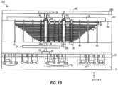
- FIG. 1A is a perspective view of a 3D-NAND memory device 100 and FIG. 1B is a cross-sectional view of the 3D-NAND memory device 100.
- the cross-sectional view of the 3D-NAND memory device 100 in FIG. 1B is obtained from a line A-A' along a Y-direction (i.e., bit line direction) of the memory device 100 in FIG. 1A .
- the memory device 100 can have a first substrate 10 that is suitable for complementary metal-oxide-semiconductor (CMOS) technology, and is referred to as CMOS substrate 10 or periphery circuit substrate 10. Circuits in the CMOS technology are formed using p-type MOS (PMOS) transistors and n-type MOS (NMOS) transistors. In some examples, the PMOS transistors and NMOS transistors are collectively referred to as CMOS transistors. A plurality of CMOS transistors are formed over a top surface 10a of the CMOS substrate 10. The CMOS transistors can form electric circuits to handle data I/O as well as memory cell operations of the memory device 100. For example, as shown in FIG. 1A , a plurality of NMOS transistors 12 and a plurality of PMOS transistors 14 are formed on a top portion of the CMOS substrate 10.
- CMOS substrate 10 complementary metal-oxide-semiconductor
- a plurality of bonding VIAs 16 are formed over the CMOS transistors and electrically coupled to the CMOS transistors.
- the bonding VIAs 16 can be electrically connected to gates, source regions, or drain regions of the CMOS transistors.
- the memory device 100 further includes a second substrate 18 that is suitable for memory cells and is referred to as cell array substrate 18.
- a memory cell stack can be formed over a top surface 18a of the cell array substrate 18, and a plurality of bottom source lines 34 can be formed over an opposing bottom surface 18b of the cell array substrate 18.
- the bottom source lines 34 are connected to form a bottom source line mesh, and the bottom source line mesh can also be referred to as a bottom connection structure.
- the memory cell stack includes two or more n-well regions 30 (shown as 30a and 30b in Fig. 1A ) that extend into the cell array substrate 18 from the top surface 18a.
- the n-well regions 30 are coupled to the bottom source lines 34 through a plurality of first VIAs 32 that extends from the bottom surface 18b of the cell array substrate 18 to the n-well regions 30.
- Two or more array common source (ACS) structures 28 that extend from the n-well regions 30 toward the top surface 10a of the CMOS substrate 10 and are coupled to the n-well regions 30.
- Each of the two or more n-well regions 30 can be in direct contact with a respective ACS structure.
- a plurality of M1 routing lines 24 are positioned between the ACS structures 28 and a plurality of top source lines 20.
- the top source lines 20 are connected to form a top source line mesh, and the top source line mesh can also be referred to as a top connection structure.
- the M1 routing lines 24 are coupled to the ACS regions 28 through a plurality of second VIAs 26.
- an ACS structure 28a can connect to a M1 routing line 24 through a second VIA 26.
- the M1 routing lines include a plurality of bit lines that are coupled to a plurality of channel structures 38.
- the channel structures 38 are illustrated in FIG. 1B .
- the top source lines 20 are formed over the M1 routing lines 24 and coupled to the M1 routing lines through a plurality of third VIAs 22.
- a top source line 20 is electrically connected to a M1 routing line 24 through a third VIA 22.
- the top surface 18a of the cell array substrate 18 and the top surface 10a of the CMOS substrate 10 are aligned facing each other so that the transistors are coupled to the top source lines 20 through the bonding VIAs 16.
- a source line 20 is electrically connected to a PMOS transistor 14 through a bonding VIA 16.
- the cell array substrate 18 can include a p-well region 36 that is formed in a top region of the cell array substrate 18, where the n-well regions 30 can be positioned in the p-well region 36.
- the p-well region 36 can extend into the cell array substrate 18 from the top surface 18a with a depth from 0.5 um to 5 um according to the design requirements.
- the p-well is also known as 'active tub' since voltages are applied to the tub during erasing or programming the memory device 100.
- the p-well can be also configured to isolate the memory cell stack from adjacent components.
- a top source line 20 is electrically coupled to one or more CMOS transistors, such as one of the PMOS transistors 14, through one or more bonding VIAs 16.
- An M1 routing line 24 is electrically coupled to the top source line 20 through a third VIA 22.
- the ACS structure 28a is electrically coupled to M1 routing line 24 through a second VIAs 26.
- An n-well region 30a is in contact with an ACS structures 28a.
- the n-well regions 30 further extend into the cell array substrate 18 from the top surface 18a.
- the first VIAs 32 extend into the cell array substrate 18 from the bottom surface 18b to the n-well regions 30.
- the bottom source lines 34 are formed over the first VIAs 32 and in direct contact with the first VIAs 32.
- the memory device 100 also includes the plurality of channel structures 38.
- the channel structures 38 protrude from the top surface 18a of the cell array substrate 18 along a height direction (Z-direction) that are perpendicular to the cell array substrate 18.
- a plurality of word lines 42 are positioned over the top surface 18a of the cell array substrate18 with a staircase configuration, and are spaced apart from each other by a plurality of insulating layers 44.
- the channel structures 38 extend through the plurality of word lines 42 and the plurality of the insulation layers 44.
- the channel structures 38 are electrically coupled to M1 routing lines 24 through top channel contacts (not shown). In the Fig.
- the M1 routing lines 24 that are connected to the channel structures 38 are configured as bit lines for the memory cell array, and can be referred to as bit lines 24.
- the M1 routing lines 24 extend in a length direction (Y-direction) of the cell array substrate 18.
- the ACS structures 28 extend through the plurality of word lines 42 and the plurality of insulating layers 44 along the height direction, and further extend in a width direction (X-direction) of the cell array substrate 18.
- the plurality of the channel structures 38 are separated by the ACS regions 28.
- the memory device 100 also includes a plurality of dummy channel structures 40.
- the dummy channel structures 40 protrude from the top surface 18a of the cell array substrate 18 along the height direction of the cell array substrate 18. Some of the dummy channel structures 40 can further extend through the word lines 42 and insulating layers 44.
- the ACS structures 28 have a top portion 28' that is made of tungsten, and a bottom portion 28'' that is made of polysilicon.
- the channel structures 38 can have a cylindrical shape with sidewalls and a bottom region. Of course, other shapes are possible.
- the channel structures 38 are formed along the height direction of the cell array substrate 18, and electrically coupled with the cell array substrate 18 VIA bottom channel contacts 48 of the channel structures 38.
- Each of the channel structures 38 further includes a respective channel layer, a respective tunneling layer, a respective charge trapping layer, and a respective barrier layer. For simplicity and clarity, the channel layer, tunneling layer, charge trapping layer, and barrier layer are not shown in FIG. 1B .
- the top source lines 20 and the bottom source lines 34 are electrically connected through one or more through silicon VIAs (TSVs) that are not shown in FIGS. 1A and 1B .
- TSVs through silicon VIAs
- a plurality of spacer layers 50 are formed between the first VIAs 32 and the cell array substrate 18 in order to isolates the first VIAs 32 from the cell array substrate 18.
- the spacer layers 50 can be a dielectric layer, such as a Tetraethyl orthosilicate (TEOS) layer.
- TEOS Tetraethyl orthosilicate
- the first VIAs 32 can have an extended wall-shape that has a tapered cross section, a frustoconical shape, or other suitable shapes.
- a plurality of fourth VIAs can be formed over the top source lines 20.
- the fourth VIAs can be bonded with the bonding VIAs 16 subsequently so that the top source lines 20 are coupled to the transistors through the bonded fourth and bonding VIAs.
- a plurality of n+ regions can be arranged between the first VIAs 32 and the n-well regions 30 to improve conductivity between the first VIAs 32 and the n-well regions 30.
- Each of the n+ regions can be disposed between a respective first VIA and a respective n-well region 30.
- the n-well regions 30 can be doped through an ion implantation process with phosphorus at a dopant concentration from 10e11 cm -3 to 10e14 cm -3 .
- the N+ regions can be doped with phosphorus at a dopant concentration from 10e14 cm -3 to 10e18 cm -3 .
- a dielectric layer 46 can be formed over the bottom surface 18b of the cell array wafer 18, and the bottom source lines 34 are formed in the dielectric layer 46. Further, an insulating layer (not shown) can be disposed between the bottom surface 18b of the cell array wafer 18 and the bottom source lines 34 so that the bottom source lines 34 are spaced apart from the cell array 18. Accordingly, the second VIAs 32 can extend through the insulating layer, and further extend into the cell array wafer 18 from the bottom surface 18b.
- the first VIAs 32 can be made of Cu, W, Ru, or other suitable material.
- a barrier layer can be disposed between the first VIAs 32 and the spacer layers 50.
- the barrier layer can be made of Ta, TaN, Ti, TiN, or other suitable materials.
- the top source lines 20 and the bottom source lines 34 can be made of Cu, Al, W, or other suitable materials.
- FIGS. 1A and 1B are merely exemplary embodiments of the disclosed 3D-NAND memory device 100.
- the 3D-NAND memory device can include other components, structures, and dimensions according to different design requirements.
- FIG. 2 is a schematic perspective view of a related 3D-NAND memory device 200 in three-dimensions, in accordance with exemplary embodiments of the disclosure.
- the memory device 200 has a CMOS substrate 70.
- a plurality of CMOS transistors are formed over a top surface 70a of the CMOS substrate 70.
- the CMOS transistors can include NMOS transistors 72 and PMOS transistors 74.
- a plurality of bonding VIAs 76 are formed over the CMOS transistors and electrically coupled to the CMOS transistors.
- the bonding VIAs 76 can be electrically connected to source regions, drain regions, or gates of the CMOS transistors.
- a cell array substrate 80 is positioned over the bonding VIAs 76.
- Two or more n-well regions 78 are formed in the cell array substrate 80.
- the n-well regions 78 extend into the cell array substrate 80 from a top surface 80a.
- a p-well region 94 is formed in the cell array substrate 80.
- two or more ACS structures 82 are formed in a top position of the cell array substrate 80.
- two or more ACS structures 82 are formed. Each of the n-well regions 78 is in direct contact with a respective ACS structure 82.
- a plurality of M1 VIAs 88 are formed.
- a plurality of M1 routing lines 86 are arranged over the ACS structures 82.
- the M1 routing lines 86 are coupled to the ACS structures 82 through the M1 VIAs 88.
- a plurality of M2 VIAs 90 are formed over the M1 routing lines 86.
- a plurality of source lines (or a source line mesh) 92 are formed.
- the source lines 92 are electrically coupled to the M1 routing lines 86 through the M2 VIAs 90.
- the memory device 200 further includes a plurality of channel regions 84.
- the channel regions 84 protrude from the top surface 80a and extend along of a height direction (Z-direction) of the cell array substrate 80.
- the channel structures 84 are positioned below the M1 routing lines 86 and electrically coupled to the M1 routing lines through top channel contacts (not shown).
- the M1 routing lines that are connected to the channel structures can be named as bit lines.
- the memory device 200 further includes a plurality of word lines (not shown in FIG. 2 ) formed over the top surface 80a of the cell array substrate 80.
- the word lines are spaced apart from each other by a plurality of insulating layers (not shown in FIG. 2 ).
- the channel structures 84 extend through the word lines and the insulating layers.
- the ACS structures 82 also extend through the word lines and the insulating layers.
- the channel structures 84 and the n-well regions 78 can be electrically coupled to the CMOS transistors formed in the CMOS substrate 70 through the bonding VIAs 76.
- an input voltage can be applied to the n-well regions 78 through a conductive channel that is formed by the source lines 92, the M2 VIAs 90, the M1 routing lines 86, the M1 VIAs 88, and the ACS structures 82.
- the ACS structures 82 typically are wall-shaped line contacts along a word line direction (X-direction) of the cell array substrate 80. Such a wall-shaped contact needs sufficient conductivity to prevent an arising ground noise during sensing operations.
- a height of the ACS structures also increases.
- the increased height of the ACS structures results in an increased resistance of the ACS structures.
- a width of the ACS structures can be increased, which in turn impacts a die size and wafer mechanical stability due to high tungsten stress.
- Figures 3A through 7 are perspective and cross-sectional views of various intermediary steps of manufacturing the 3D-NAND memory device 100, in accordance with exemplary embodiments of the disclosure.
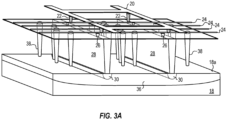
- FIG. 3A is a schematic perspective view of a memory cell stack that is formed over the cell array substrate 18.
- the memory cell stack can be formed through a variety of semiconductor manufacturing processes.
- the semiconductor manufacturing processes can include a photolithography process, a dry etching process, a wet etching process, a wet clean process, an implantation process, a film deposition process (i.e., CVD, PVD, diffusion, electroplating), a surface planarization process (i.e., CMP), and other suitable semiconductor manufacturing processes.
- the memory stack can have a similar configuration that is illustrated in FIG. 1A .
- the memory stack can includes the n-well regions 30 that extend from the top surface 18a into the cell array substrate 18.
- the ACS structures 28 are formed over the n-well regions 30 and in contact with the n-well regions.
- the ACS regions 28 and the M1 routing lines 24 are electrically connected through the second VIAs 26.
- the top source lines (source line mesh) 20 are electrically connected to the M1 routing lines 24 through the third VIAs 22.
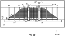
- FIG. 3B is a cross-sectional view of the memory cell stack that has a similar configuration illustrated in FIG. 1B .
- the memory cells stack further includes the channel regions 38 and the dummy channel regions 40.
- the channel regions 38 and dummy channel regions 40 protrude from the top surface 18a and extend along of the height direction of the cell array substrate 18.
- the channel structures 38 are positioned below the M1 routing lines 24 and electrically coupled to the M1 routing lines 24 through the top channel contacts (not shown).
- the M1 routing lines that are connected to the channel structures can be named as bit lines.
- the memory cell stack further includes the word lines 42 formed over the top surface 18a of the cell array substrate 18.
- the word lines 42 are spaced apart from each other by the insulating layer 44.
- the channel structures 38 extend through the word lines 42 and the insulating layers 44.
- the ACS structures 28 also extend through the word lines 42 and the insulating layers 44.
- the memory cell stack can be flipped upside down and the bottom surface 18b of the cell array substrate 18 is exposed.
- a subsequent surface removal process such as a CMP process, an etching process, or a combination thereof, can be applied to remove a portion of the cell array substrate 18 from the bottom surface 18b. After the surface removal process, the thickness of the cell array substrate 18 is reduced.
- the plurality of first VIAs 33 can be formed through a variety of semiconductor manufacturing processes that include a photolithography process, an etching process, a film deposition process (i.e., CVD, electroplating), and a surface planarization process.
- a patterned mask layer can be formed over the bottom surface 18b of the cell array substrate 18 through the photolithography process.
- a dry etching process can transfer patterns in the mask layer into the cell array substrate to form a plurality of VIA openings.
- a spacer layer 50 can be deposited in the VIA openings and a conductive layer (i.e., Cu) can be formed over the spacer layer 50 to fill the VIA openings through an electroplating process.
- a subsequent surface planarization process, such as CMP, can be applied to remove excessive Cu over the bottom surface of the cell array substrate.
- the conductive layer that remains in the VIA openings become the first VIAs 32.
- the first VIAs 32 extend into the cell array substrate 18 from the bottom surface 18b and land on the n-well regions 30 so as to form electrical connection.
- the second VIAs 32 can be made of Cu, W, Ru, or the like.
- a barrier layer (not shown) can be formed between the spacer layers 50 and the first VIAs 32.
- the barrier layer can be made of Ti, TiN, TaN, Ta, or other suitable materials.
- a plurality of n+ regions can be formed at exposed area of the n-well regions when the n-well regions are exposed by the plurality of VIA openings.
- the n+ regions can be made by an ion implantation process.
- the spacer layer 50, and the conductive layer can be subsequently deposited in the VIA openings.
- the bottom source lines 34 can be formed over the bottom surface 18a of the cell array substrate 18.
- a dielectric layer 46 such as SiO
- a subsequent photolithography process can be applied to form trench openings in the dielectric layer 46.
- a film deposition process can then be applied to fill the trench openings with conductive material, such as Cu, Al, W, or the like.
- a subsequent CMP process can be applied to remove excessive the conduction material over a top surface of the dielectric layer 46. The conductive material that remains in the trench openings form the bottom source lines 34.
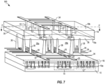
- the plurality of CMOS transistors such as PMOS 14 and NMOS 12, can be formed over the top surface 10a of the CMOS substrate 10.
- the plurality of bonding VIAs 16 can be formed over the CMOS transistors.
- the cell array substrate 18 and the CMOS substrate 10 can be bonded together through the bonding VIAs 16.
- the top surface 10a of the CMOS substrate 10 and the top surface 18a of the cell array substrate 18 are aligned facing each other so that the transistors are coupled to the top source lines 20 through the bonding VIAs 16.
- the 3D-NAND memory device 100 is formed, which has a same configuration as the memory device shown in FIGS. 1A and 1B .
- the fourth VIAs are formed over the top source lines 20, and the fourth VIAs are connected to the bonding VIAs 16 so that the cell array substrate 18 and the CMOS substrate 10 are bonded together.
- a plurality of TSVs can also be formed.
- the TSVs can extend into the cell array substrate 18 from the bottom surface 18b of the cell array substrate 18, and connect the top source lines 20 and bottom source lines 34.
- FIG. 8 is a flowchart of an exemplary process for manufacturing the 3D-NAND memory device 100, in accordance with embodiments of the disclosure.
- the process 800 begins at step 810 where a memory cell stack can be formed over a top surface of a first substrate.
- the first substrate further has an opposing bottom surface.
- the memory cell stack includes two or more n-well regions formed in the first substrate.
- the two or more n-well regions extend into the first substrate from the top surface.
- the memory stack can also include two or more ACS structures formed over the two or more n-well regions. Each of the ACS structures is in direct contact with a respective n-well region.
- a plurality of M1 routing lines are formed over the ACS structures.
- the M1 routing lines are electrically coupled to the ACS structures through a plurality of M1 VIAs. Further, a plurality of top source lines formed over the plurality of M1 routing lines. The M1 routing lines are electrically coupled to the top source lines through a plurality of M2 VIAs. In some embodiments, step 810 can be performed as illustrated with reference to FIGS. 3A-3B .
- step 820 a portion of the first substrate can be removed from the bottom surface of the first substrate.
- the bottom portion of the first substrate can be removed through an etching process, a CMP process, or the like, or a combination thereof.
- step 820 can be performed as illustrated with reference to FIGS. 4A-4B .
- step 830 a plurality of VIA contacts can be formed that extend into the first substrate from the bottom surface to contact the n-well regions.
- a plurality of bottom source lines can be formed over the VIA contacts. The plurality of bottom source lines are electrically connected to the n-well regions through the VIA contacts.
- step 830 can be performed as illustrate with reference to FIGS. 5A-6B .
- step 840 a plurality of transistors are formed over a top surface of a second substrate, a plurality of bonding VIAs are formed over the transistors. Further, the first substrate and the second substrate are bonded together through the bonding VIAs. The top surface of the first substrate and the top surface of the second substrates are aligned facing each other so that the transistors are coupled to the top source lines through the bonding VIAs.
- step 830 can be performed as illustrate with reference to FIG. 7 .
- interconnect structures e.g., metallization layers having conductive lines and/or VIAs
- Such interconnect structures electrically connect the semiconductor device 100 with other contact structures and/or active devices to form functional circuits. Additional device features such as passivation layers, input/output structures, and the like may also be formed.
- an input voltage is applied to a n-well region through a conductive channel that is formed by a source line, a M1 routing line, an ACS structure, and the n-well region.
- a resistance of the conductive channel is inevitably affected by a resistance of the ACS structure.
- a height of a 3D NAND stack increases with density, a height of the ACS region accordingly grows.
- the resistance of the ACS region inevitably increases in the height direction of the 3D NAND stack.
- the increased resistance of the ACS region results in an elevated resistance of the conductive channel.
- the elevated resistance of the conductive channel accordingly can cause ground noise arising in sensing operations of the related memory devices.
- the source lines can be electrically coupled to the n-well regions from a polished backside (i.e., the bottom surface) of the cell array substrate. Accordingly, a resistance of source lines to n-well regions can be decreased. The decreased resistance of source lines to n-well regions can reduce the ground noise.
- the resistance of the ACS structures does not impact a source side resistance of the memory device and the ground noise.
- the disclosed structure can eliminate gaps between M1 routing lines that are used to add contacts to connect the source line mesh and the ACS structures, which in turn helps a reduction of die size in a word line direction.
Landscapes
- Non-Volatile Memory (AREA)
- Semiconductor Memories (AREA)
Claims (10)
- 3D-NAND-Speichervorrichtung (100), die Folgendes aufweist:ein erstes Substrat (10) mit einer ersten Seite, auf der ein Speicherstapel ausgebildet ist, und einer zweiten Seite, die der ersten Seite gegenüberliegt;einen dotierten Bereich, der in der ersten Seite des ersten Substrats (10) ausgebildet ist und elektrisch mit mindestens einem Source-Anschluss eines Speichertransistors gekoppelt ist, der auf der ersten Seite des ersten Substrats (10) ausgebildet ist;eine erste Verbindungsstruktur, die über der zweiten Seite des ersten Substrats (10) ausgebildet ist und mit dem dotierten Bereich über eine erste Durchkontaktierung (32, 33) gekoppelt ist, wobei sich die erste Durchkontaktierung (32, 33) von der zweiten Seite des ersten Substrats (10) zu dem dotierten Bereich erstreckt;eine gemeinsame Source-Struktur (28), die über dem dotierten Bereich ausgebildet und mit diesem gekoppelt ist, wobei die gemeinsame Source-Struktur (28) einen oberen Abschnitt (28'), der aus Wolfram besteht, und einen unteren Abschnitt (28"), der aus Polysilizium besteht, aufweist;eine Bitleitung, die über der gemeinsamen Source-Struktur (28) ausgebildet ist und mit der gemeinsamen Source-Struktur (28) über eine zweite Durchkontaktierung gekoppelt ist;
eine zweite Verbindungsstruktur, die über der Bitleitung positioniert ist und über eine dritte Durchkontaktierung (22) mit der Bitleitung gekoppelt ist, wobei die erste Verbindungsstruktur und die zweite Verbindungsstruktur miteinander gekoppelt sind;eine Vielzahl von Kanalstrukturen (38, 84), die sich von der ersten Seite des ersten Substrats (10) erstrecken; undeine Vielzahl von Wortleitungen (42), die über der ersten Seite des ersten Substrats (10) in einer treppenförmigen Konfiguration positioniert sind, wobei:
die Vielzahl der Wortleitungen (42) durch eine Vielzahl von Isolierschichten (44) voneinander beabstandet sind,die Vielzahl der Kanalstrukturen (38, 84) sich durch die Vielzahl der Wortleitungen und die Vielzahl der Isolierschichten erstreckt,die Vielzahl der Kanalstrukturen (38, 84) unter der Bitleitung angeordnet ist unddie gemeinsame Source-Struktur sich durch die Vielzahl der Wortleitungen und die Vielzahl der Isolationsschichten (44) erstreckt und trennt die Vielzahl der Kanalstrukturen (38, 84) trennt. - 3D-NAND-Speichervorrichtung (100) nach Anspruch 1, ferner umfassend:einen Transistor, der in einer ersten Seite eines zweiten Substrats (18) ausgebildet ist; undeine Bonding-Durchkontaktierung (16, 76), die über dem Transistor ausgebildet und mit diesem gekoppelt ist,
wobei die erste Seite des ersten Substrats (10) und die erste Seite des zweiten Substrats (18) so ausgerichtet sind, dass sie einander zugewandt sind, so dass der Transistor durch die Bonding-Durchkontaktierung (16, 76) mit der zweiten Verbindungsstruktur gekoppelt ist,wobei eine vierte Durchkontaktierung zwischen der zweiten Verbindungsstruktur und der Bonding-Durchkontaktierung (16, 76) angeordnet ist. - 3D-NAND-Speichervorrichtung (100) nach Anspruch 1, wobei sich die erste Durchkontaktierung (32, 33) durch den dotierten Bereich erstreckt und mit der gemeinsamen Source-Struktur in Kontakt steht.
- 3D-NAND-Speichervorrichtung (100) nach Anspruch 1, ferner umfassend: eine Abstandsschicht (50), die zwischen der ersten Durchkontaktierung (32, 33) und dem ersten Substrat (10) angeordnet ist, isoliert die erste Durchkontaktierung (32, 33) von dem ersten Substrat (10).
- 3D-NAND-Speichervorrichtung (100) nach Anspruch 1, ferner umfassend: einen n+-Bereich, der zwischen der ersten Durchkontaktierung (32, 33) und dem dotierten Bereich angeordnet ist, wobei der dotierte Bereich vom n-Typ ist.
- 3D-NAND-Speichervorrichtung (100) nach Anspruch 1, wobei die erste Durchkontaktierung (32, 33) zumindest eine erweiterte Wandform mit einem sich verjüngenden Querschnitt oder einer kegelstumpfförmigen Form aufweist.
- Verfahren zur Herstellung einer 3D-NAND-Speichervorrichtung (100), das folgende Schritte aufweist:Bilden einer ersten Durchkontaktierung (32, 33), die sich von einer zweiten Seite eines ersten Substrats (10) erstreckt, wobei das erste Substrat (10) eine gegenüberliegende erste Seite aufweist, auf der ein Speicherstapel ausgebildet ist, wobei der Speicherstapel einen dotierten Bereich aufweist, der in der ersten Seite des ersten Substrats (10) angeordnet ist und elektrisch mit mindestens einem Source-Anschluss eines Transistors gekoppelt ist, der in der ersten Seite des ersten Substrats (10) ausgebildet ist, und wobei die erste Durchkontaktierung (32, 33) elektrisch mit dem dotierten Bereich verbunden ist;
Bilden einer ersten Verbindungsstruktur über der ersten Durchkontaktierung (32, 33), so dass die erste Verbindungsstruktur mit dem dotierten Bereich über die erste Durchkontaktierung (32, 33) gekoppelt ist;Bilden einer gemeinsamen Source-Struktur (28) über dem dotierten Bereich und gekoppelt an den dotierten Bereich, wobei die gemeinsame Source-Struktur (28) einen oberen Abschnitt (28'), der aus Wolfram besteht, und einen unteren Abschnitt (28"), der aus Polysilizium besteht, aufweist;Bilden einer Bitleitung über der gemeinsamen Source-Struktur (28), wobei die Bitleitung über eine zweite Durchkontaktierung mit der gemeinsamen Source-Struktur (28) gekoppelt ist;Bilden einer zweiten Verbindungsstruktur über der Bitleitung, wobei die zweite Verbindungsstruktur über eine dritte Durchkontaktierung (22) mit der Bitleitung gekoppelt ist, wobei die erste Verbindungsstruktur und die zweite Verbindungsstruktur miteinander gekoppelt sind;Bilden einer Vielzahl von Kanalstrukturen (38, 84), die sich von der ersten Seite des ersten Substrats (10) erstrecken; undBilden einer Vielzahl von Wortleitungen (42), die über der ersten Seite des ersten Substrats (10) in einer treppenförmigen Konfiguration positioniert sind, wobei:die Vielzahl der Wortleitungen (42) durch eine Vielzahl von Isolierschichten (44) voneinander beabstandet sind,die Vielzahl der Kanalstrukturen (38, 84) sich durch die Vielzahl er Wortleitungen und die Vielzahl der Isolierschichten erstreckt,
die Vielzahl der Kanalstrukturen (38, 84) unterhalb der Bitleitung angeordnet ist unddie gemeinsame Source-Struktur sich durch die Vielzahl der Wortleitungen und die Vielzahl der Isolierschichten (44) erstreckt und die Vielzahl der Kanalstrukturen (38, 84) trennt. - Verfahren nach Anspruch 7, wobei das Bilden der ersten Verbindungsstruktur über der ersten Durchkontaktierung (32, 33) ferner folgende Schritte aufweist:Entfernen eines Teils des ersten Substrats (10) von der zweiten Seite des ersten Substrats (10);Bilden der ersten Durchkontaktierung (32, 33), die sich von der zweiten Seite des ersten Substrats (10) zu dem dotierten Bereich erstreckt; undBilden der ersten Verbindungsstruktur über der ersten Durchkontaktierung (32, 33).
- Verfahren nach Anspruch 8, wobei die erste Durchkontaktierung (32, 33) zumindest eine erweiterte Wandform mit einem sich verjüngenden Querschnitt oder einer kegelstumpfförmigen Form aufweist,
oder wobei das Verfahren ferner folgenden Schritt aufweist:
Bilden eines n+-Bereichs zwischen der ersten Durchkontaktierung (32, 33) und dem dotierten Bereich, wobei der dotierte Bereich vom n-Typ ist. - Verfahren nach Anspruch 8, das ferner folgende Schritte aufweist:Bilden eines Transistors über einer ersten Seite eines zweiten Substrats (18); Bilden einer Bonding-Durchkontaktierung (16, 76) über dem Transistor, wobei die Bonding-Durchkontaktierung (16, 76) elektrisch mit dem Transistor gekoppelt ist; und
Bonden des ersten Substrats (10) und des zweiten Substrats (18) durch die Bonding-Durchkontaktierung (16, 76), wobei die zweite Verbindungsstruktur mit dem Transistor ausgerichtet ist und durch die Bonding-Durchkontaktierung (16, 76) mit dem Transistor gekoppelt ist,oder wobei das Verfahren ferner umfasst:
Bilden einer Durchgangs-Silizium-Durchkontaktierung (TSV), die sich von der zweiten Seite des ersten Substrats (10) zur ersten Seite des ersten Substrats (10) erstreckt, wobei die erste Verbindungsstruktur und die zweite Verbindungsstruktur durch die TSV elektrisch verbunden sind.
Priority Applications (1)
| Application Number | Priority Date | Filing Date | Title |
|---|---|---|---|
| EP25153819.5A EP4521880A3 (de) | 2019-06-27 | 2019-06-27 | Neuartige 3d-nand-speichervorrichtung und verfahren zur formung davon |
Applications Claiming Priority (1)
| Application Number | Priority Date | Filing Date | Title |
|---|---|---|---|
| PCT/CN2019/093179 WO2020258130A1 (en) | 2019-06-27 | 2019-06-27 | Novel 3d nand memory device and method of forming the same |
Related Child Applications (1)
| Application Number | Title | Priority Date | Filing Date |
|---|---|---|---|
| EP25153819.5A Division EP4521880A3 (de) | 2019-06-27 | 2019-06-27 | Neuartige 3d-nand-speichervorrichtung und verfahren zur formung davon |
Publications (3)
| Publication Number | Publication Date |
|---|---|
| EP3915147A1 EP3915147A1 (de) | 2021-12-01 |
| EP3915147A4 EP3915147A4 (de) | 2022-11-23 |
| EP3915147B1 true EP3915147B1 (de) | 2025-01-29 |
Family
ID=68544595
Family Applications (2)
| Application Number | Title | Priority Date | Filing Date |
|---|---|---|---|
| EP25153819.5A Pending EP4521880A3 (de) | 2019-06-27 | 2019-06-27 | Neuartige 3d-nand-speichervorrichtung und verfahren zur formung davon |
| EP19935559.5A Active EP3915147B1 (de) | 2019-06-27 | 2019-06-27 | Neuartige 3d-nand-speichervorrichtung und verfahren zu ihrer herstellung |
Family Applications Before (1)
| Application Number | Title | Priority Date | Filing Date |
|---|---|---|---|
| EP25153819.5A Pending EP4521880A3 (de) | 2019-06-27 | 2019-06-27 | Neuartige 3d-nand-speichervorrichtung und verfahren zur formung davon |
Country Status (7)
| Country | Link |
|---|---|
| US (4) | US11088166B2 (de) |
| EP (2) | EP4521880A3 (de) |
| JP (1) | JP7292403B2 (de) |
| KR (3) | KR102923273B1 (de) |
| CN (2) | CN110494979B (de) |
| TW (1) | TWI703711B (de) |
| WO (1) | WO2020258130A1 (de) |
Families Citing this family (23)
| Publication number | Priority date | Publication date | Assignee | Title |
|---|---|---|---|---|
| EP4521880A3 (de) * | 2019-06-27 | 2025-05-14 | Yangtze Memory Technologies Co., Ltd. | Neuartige 3d-nand-speichervorrichtung und verfahren zur formung davon |
| KR102848950B1 (ko) * | 2019-09-24 | 2025-08-20 | 삼성전자주식회사 | 집적회로 소자 |
| CN111316442B (zh) * | 2020-01-28 | 2021-05-14 | 长江存储科技有限责任公司 | 三维存储器件及用于形成三维存储器件的方法 |
| CN112701121B (zh) | 2020-01-28 | 2023-09-12 | 长江存储科技有限责任公司 | 三维存储器件及用于形成三维存储器件的方法 |
| WO2021163944A1 (en) * | 2020-02-20 | 2021-08-26 | Yangtze Memory Technologies Co., Ltd. | Dram memory device with xtacking architecture |
| CN112352315B (zh) * | 2020-04-14 | 2022-10-11 | 长江存储科技有限责任公司 | 具有背面互连结构的三维存储器件 |
| WO2021208268A1 (en) | 2020-04-14 | 2021-10-21 | Yangtze Memory Technologies Co., Ltd. | Three-dimensional memory device with backside interconnect structures |
| EP4136675B1 (de) * | 2020-04-14 | 2025-07-16 | Yangtze Memory Technologies Co., Ltd. | Verfahren zur herstellung einer dreidimensionalen speichervorrichtung mit rückseitigem source-kontakt |
| CN111566815B (zh) * | 2020-04-14 | 2021-09-14 | 长江存储科技有限责任公司 | 具有背面源极触点的三维存储器件 |
| TWI780473B (zh) * | 2020-07-07 | 2022-10-11 | 大陸商長江存儲科技有限責任公司 | 具有背面互連結構的立體記憶體元件以及其形成方法 |
| EP4694614A3 (de) * | 2020-07-31 | 2026-04-08 | Yangtze Memory Technologies Co., Ltd. | Verfahren zur herstellung von kontaktstrukturen und halbleiterbauelemente dafür |
| KR102881083B1 (ko) * | 2020-09-23 | 2025-11-06 | 삼성전자주식회사 | 반도체 장치 및 이를 포함하는 전자 시스템 |
| KR102874826B1 (ko) | 2020-10-22 | 2025-10-22 | 삼성전자주식회사 | 반도체 메모리 장치, 이를 포함하는 전자 시스템 및 이의 제조 방법 |
| KR102898249B1 (ko) * | 2020-11-13 | 2025-12-11 | 삼성전자주식회사 | 반도체 장치 및 이를 포함하는 데이터 저장 시스템 |
| JP2022118667A (ja) * | 2021-02-02 | 2022-08-15 | キオクシア株式会社 | 半導体記憶装置 |
| TWI800024B (zh) * | 2021-02-05 | 2023-04-21 | 旺宏電子股份有限公司 | 半導體裝置及其操作方法 |
| KR102885144B1 (ko) * | 2021-02-23 | 2025-11-14 | 삼성전자주식회사 | 가변 저항 메모리 장치 |
| US12255143B2 (en) * | 2021-02-26 | 2025-03-18 | Micron Technology, Inc. | Microelectronic devices including composite pad structures on staircase structures, and related methods, memory devices, and electronic systems |
| CN113078164B (zh) * | 2021-03-26 | 2022-04-15 | 长江存储科技有限责任公司 | 一种半导体器件 |
| KR102950736B1 (ko) | 2022-06-22 | 2026-04-08 | 삼성전자주식회사 | 집적회로 소자 및 이를 포함하는 전자 시스템 |
| CN115172268B (zh) * | 2022-07-04 | 2025-10-14 | 中微半导体设备(上海)股份有限公司 | 一种在高深宽比结构中沉积钨的方法及其半导体基片 |
| JP2024044686A (ja) * | 2022-09-21 | 2024-04-02 | キオクシア株式会社 | 半導体記憶装置 |
| US20250380512A1 (en) * | 2024-06-07 | 2025-12-11 | Taiwan Semiconductor Manufacturing Company, Ltd. | Multi-finger mos circuit, method of manufacturing the same, and system |
Citations (1)
| Publication number | Priority date | Publication date | Assignee | Title |
|---|---|---|---|---|
| CN109860197A (zh) * | 2019-02-27 | 2019-06-07 | 长江存储科技有限责任公司 | 三维存储器及形成三维存储器的方法 |
Family Cites Families (39)
| Publication number | Priority date | Publication date | Assignee | Title |
|---|---|---|---|---|
| JP3199969B2 (ja) | 1994-12-13 | 2001-08-20 | キヤノン株式会社 | 多点測距装置 |
| JPH08186235A (ja) | 1994-12-16 | 1996-07-16 | Texas Instr Inc <Ti> | 半導体装置の製造方法 |
| JPH08227980A (ja) | 1995-02-21 | 1996-09-03 | Toshiba Corp | 半導体装置及びその製造方法 |
| US7772632B2 (en) | 2006-08-21 | 2010-08-10 | Micron Technology, Inc. | Memory arrays and methods of fabricating memory arrays |
| US7875529B2 (en) | 2007-10-05 | 2011-01-25 | Micron Technology, Inc. | Semiconductor devices |
| US20090242955A1 (en) * | 2008-03-31 | 2009-10-01 | Qimonda Ag | Integrated Circuit, Memory Device and Methods of Manufacturing the Same |
| US20110115018A1 (en) | 2009-11-13 | 2011-05-19 | Maxim Integrated Products, Inc. | Mos power transistor |
| KR101800438B1 (ko) | 2010-11-05 | 2017-11-23 | 삼성전자주식회사 | 3차원 반도체 장치 및 그 제조 방법 |
| KR101952272B1 (ko) | 2012-11-06 | 2019-02-26 | 삼성전자주식회사 | 반도체 기억 소자 |
| JP6203152B2 (ja) * | 2014-09-12 | 2017-09-27 | 東芝メモリ株式会社 | 半導体記憶装置の製造方法 |
| KR102415401B1 (ko) * | 2015-05-21 | 2022-07-01 | 삼성전자주식회사 | 3차원 반도체 메모리 장치 및 그것의 동작 방법 |
| KR20170014757A (ko) | 2015-07-31 | 2017-02-08 | 에스케이하이닉스 주식회사 | 반도체 장치 및 그 제조방법 |
| US9911748B2 (en) * | 2015-09-28 | 2018-03-06 | Sandisk Technologies Llc | Epitaxial source region for uniform threshold voltage of vertical transistors in 3D memory devices |
| US9818759B2 (en) | 2015-12-22 | 2017-11-14 | Sandisk Technologies Llc | Through-memory-level via structures for a three-dimensional memory device |
| KR102649372B1 (ko) | 2016-01-08 | 2024-03-21 | 삼성전자주식회사 | 3차원 반도체 메모리 장치 |
| TWI621248B (zh) * | 2016-12-15 | 2018-04-11 | 旺宏電子股份有限公司 | 立體記憶體元件及其製作方法 |
| CN106876401B (zh) * | 2017-03-07 | 2018-10-30 | 长江存储科技有限责任公司 | 存储器件的形成方法 |
| KR102283330B1 (ko) * | 2017-03-27 | 2021-08-02 | 삼성전자주식회사 | 반도체 소자 |
| KR102332346B1 (ko) * | 2017-04-10 | 2021-12-01 | 삼성전자주식회사 | 3차원 반도체 메모리 장치 및 그의 제조 방법 |
| US10224340B2 (en) * | 2017-06-19 | 2019-03-05 | Sandisk Technologies Llc | Three-dimensional memory device having discrete direct source strap contacts and method of making thereof |
| US10176880B1 (en) * | 2017-07-01 | 2019-01-08 | Intel Corporation | Selective body reset operation for three dimensional (3D) NAND memory |
| CN107658315B (zh) * | 2017-08-21 | 2019-05-14 | 长江存储科技有限责任公司 | 半导体装置及其制备方法 |
| EP3580782A4 (de) | 2017-08-21 | 2020-12-02 | Yangtze Memory Technologies Co., Ltd. | Dreidimensionale speicherbauelemente und verfahren zur formung davon |
| CN109473441B (zh) * | 2017-08-31 | 2021-08-31 | 长江存储科技有限责任公司 | 一种3d nand存储器存储单元结构 |
| CN107658317B (zh) * | 2017-09-15 | 2019-01-01 | 长江存储科技有限责任公司 | 一种半导体装置及其制备方法 |
| US10283452B2 (en) * | 2017-09-15 | 2019-05-07 | Yangtze Memory Technology Co., Ltd. | Three-dimensional memory devices having a plurality of NAND strings |
| US10283513B1 (en) * | 2017-11-06 | 2019-05-07 | Sandisk Technologies Llc | Three-dimensional memory device with annular blocking dielectrics and method of making thereof |
| CN107968091A (zh) * | 2017-11-16 | 2018-04-27 | 长江存储科技有限责任公司 | 一种共源极钨墙与钨栅极之间高质量间隙层的3d nand制备方法 |
| US10535669B2 (en) * | 2017-11-23 | 2020-01-14 | Yangtze Memory Technologies Co., Ltd. | Three-dimensional memory devices and fabricating methods thereof |
| KR102524614B1 (ko) * | 2017-11-24 | 2023-04-24 | 삼성전자주식회사 | 반도체 메모리 소자 |
| US10147732B1 (en) * | 2017-11-30 | 2018-12-04 | Yangtze Memory Technologies Co., Ltd. | Source structure of three-dimensional memory device and method for forming the same |
| US10304852B1 (en) * | 2018-02-15 | 2019-05-28 | Sandisk Technologies Llc | Three-dimensional memory device containing through-memory-level contact via structures |
| KR102612406B1 (ko) | 2018-04-06 | 2023-12-13 | 삼성전자주식회사 | 반도체 메모리 소자 |
| KR102614849B1 (ko) | 2018-05-21 | 2023-12-18 | 삼성전자주식회사 | 지지대를 갖는 3d 반도체 소자 및 그 형성 방법 |
| CN109119426B (zh) * | 2018-09-28 | 2024-04-16 | 长江存储科技有限责任公司 | 3d存储器件 |
| CN109887920A (zh) * | 2019-02-19 | 2019-06-14 | 长江存储科技有限责任公司 | 三维存储器 |
| CN109755254A (zh) * | 2019-02-28 | 2019-05-14 | 长江存储科技有限责任公司 | 三维存储器及其制作方法 |
| JP7331119B2 (ja) * | 2019-04-15 | 2023-08-22 | 長江存儲科技有限責任公司 | 複数の機能性チップを伴う三次元nandメモリデバイスの集積 |
| EP4521880A3 (de) * | 2019-06-27 | 2025-05-14 | Yangtze Memory Technologies Co., Ltd. | Neuartige 3d-nand-speichervorrichtung und verfahren zur formung davon |
-
2019
- 2019-06-27 EP EP25153819.5A patent/EP4521880A3/de active Pending
- 2019-06-27 CN CN201980001306.XA patent/CN110494979B/zh active Active
- 2019-06-27 KR KR1020247007025A patent/KR102923273B1/ko active Active
- 2019-06-27 EP EP19935559.5A patent/EP3915147B1/de active Active
- 2019-06-27 KR KR1020217029047A patent/KR102644013B1/ko active Active
- 2019-06-27 KR KR1020267002727A patent/KR20260033552A/ko active Pending
- 2019-06-27 JP JP2021554776A patent/JP7292403B2/ja active Active
- 2019-06-27 WO PCT/CN2019/093179 patent/WO2020258130A1/en not_active Ceased
- 2019-06-27 CN CN202011459262.6A patent/CN112510052B/zh active Active
- 2019-08-15 TW TW108129062A patent/TWI703711B/zh active
- 2019-12-12 US US16/712,210 patent/US11088166B2/en active Active
-
2021
- 2021-05-26 US US17/330,594 patent/US11563029B2/en active Active
- 2021-07-01 US US17/365,684 patent/US11616077B2/en active Active
-
2023
- 2023-02-22 US US18/172,415 patent/US20230200074A1/en active Pending
Patent Citations (1)
| Publication number | Priority date | Publication date | Assignee | Title |
|---|---|---|---|---|
| CN109860197A (zh) * | 2019-02-27 | 2019-06-07 | 长江存储科技有限责任公司 | 三维存储器及形成三维存储器的方法 |
Also Published As
| Publication number | Publication date |
|---|---|
| EP4521880A3 (de) | 2025-05-14 |
| KR20210125070A (ko) | 2021-10-15 |
| KR102644013B1 (ko) | 2024-03-05 |
| EP4521880A2 (de) | 2025-03-12 |
| KR102923273B1 (ko) | 2026-02-04 |
| CN112510052B (zh) | 2023-09-12 |
| TW202101738A (zh) | 2021-01-01 |
| KR20260033552A (ko) | 2026-03-10 |
| US20210327900A1 (en) | 2021-10-21 |
| JP2022524453A (ja) | 2022-05-02 |
| US11088166B2 (en) | 2021-08-10 |
| EP3915147A4 (de) | 2022-11-23 |
| CN110494979A (zh) | 2019-11-22 |
| US20230200074A1 (en) | 2023-06-22 |
| EP3915147A1 (de) | 2021-12-01 |
| US11616077B2 (en) | 2023-03-28 |
| WO2020258130A1 (en) | 2020-12-30 |
| KR20240036110A (ko) | 2024-03-19 |
| CN110494979B (zh) | 2021-01-29 |
| TWI703711B (zh) | 2020-09-01 |
| US20200411541A1 (en) | 2020-12-31 |
| CN112510052A (zh) | 2021-03-16 |
| JP7292403B2 (ja) | 2023-06-16 |
| US20210280606A1 (en) | 2021-09-09 |
| US11563029B2 (en) | 2023-01-24 |
Similar Documents
| Publication | Publication Date | Title |
|---|---|---|
| EP3915147B1 (de) | Neuartige 3d-nand-speichervorrichtung und verfahren zu ihrer herstellung | |
| CN111801798B (zh) | 三维存储器件 | |
| CN111801799B (zh) | 用于形成三维存储器件的方法 | |
| CN112041986B (zh) | 用于形成具有用于阶梯区域的支持结构的三维存储器件的方法 | |
| JP7026707B2 (ja) | 3次元メモリデバイスのハイブリッドボンディングコンタクト構造 | |
| CN111801800B (zh) | 三维存储器件 | |
| CN112352315B (zh) | 具有背面互连结构的三维存储器件 | |
| JP7459136B2 (ja) | 三次元メモリデバイス、および三次元メモリデバイスを形成するための方法 | |
| CN112219289B (zh) | 用于形成半导体器件中的片上电容器结构的方法 | |
| CN110622305B (zh) | 电容器结构及其形成方法 | |
| CN113039643B (zh) | 半导体器件中的片上电容器及其形成方法 | |
| CN112166501B (zh) | 半导体器件中的片上电容器结构 | |
| CN112689897B (zh) | 三维存储器件的接触焊盘及其制造方法 |
Legal Events
| Date | Code | Title | Description |
|---|---|---|---|
| STAA | Information on the status of an ep patent application or granted ep patent |
Free format text: STATUS: THE INTERNATIONAL PUBLICATION HAS BEEN MADE |
|
| PUAI | Public reference made under article 153(3) epc to a published international application that has entered the european phase |
Free format text: ORIGINAL CODE: 0009012 |
|
| STAA | Information on the status of an ep patent application or granted ep patent |
Free format text: STATUS: REQUEST FOR EXAMINATION WAS MADE |
|
| 17P | Request for examination filed |
Effective date: 20210824 |
|
| AK | Designated contracting states |
Kind code of ref document: A1 Designated state(s): AL AT BE BG CH CY CZ DE DK EE ES FI FR GB GR HR HU IE IS IT LI LT LU LV MC MK MT NL NO PL PT RO RS SE SI SK SM TR |
|
| DAV | Request for validation of the european patent (deleted) | ||
| DAX | Request for extension of the european patent (deleted) | ||
| REG | Reference to a national code |
Ref country code: DE Ref legal event code: R079 Ipc: H01L0027115730 Ref document number: 602019065562 Country of ref document: DE Free format text: PREVIOUS MAIN CLASS: H01L0027115240 |
|
| A4 | Supplementary search report drawn up and despatched |
Effective date: 20221020 |
|
| RIC1 | Information provided on ipc code assigned before grant |
Ipc: H01L 23/00 20060101ALI20221014BHEP Ipc: H01L 27/11582 20170101ALI20221014BHEP Ipc: H01L 27/11575 20170101ALI20221014BHEP Ipc: H01L 27/11573 20170101AFI20221014BHEP |
|
| STAA | Information on the status of an ep patent application or granted ep patent |
Free format text: STATUS: EXAMINATION IS IN PROGRESS |
|
| 17Q | First examination report despatched |
Effective date: 20230802 |
|
| REG | Reference to a national code |
Ref legal event code: R079 Free format text: PREVIOUS MAIN CLASS: H01L0027115730 Ref country code: DE Ref legal event code: R079 Ref document number: 602019065562 Country of ref document: DE Free format text: PREVIOUS MAIN CLASS: H01L0027115730 Ipc: H01L0023000000 |
|
| RIC1 | Information provided on ipc code assigned before grant |
Ipc: H10B 43/50 20230101ALI20240726BHEP Ipc: H10B 43/40 20230101ALI20240726BHEP Ipc: H10B 43/27 20230101ALI20240726BHEP Ipc: H01L 23/00 20060101AFI20240726BHEP |
|
| GRAP | Despatch of communication of intention to grant a patent |
Free format text: ORIGINAL CODE: EPIDOSNIGR1 |
|
| STAA | Information on the status of an ep patent application or granted ep patent |
Free format text: STATUS: GRANT OF PATENT IS INTENDED |
|
| INTG | Intention to grant announced |
Effective date: 20241008 |
|
| GRAS | Grant fee paid |
Free format text: ORIGINAL CODE: EPIDOSNIGR3 |
|
| P01 | Opt-out of the competence of the unified patent court (upc) registered |
Free format text: CASE NUMBER: APP_61760/2024 Effective date: 20241119 |
|
| GRAA | (expected) grant |
Free format text: ORIGINAL CODE: 0009210 |
|
| STAA | Information on the status of an ep patent application or granted ep patent |
Free format text: STATUS: THE PATENT HAS BEEN GRANTED |
|
| AK | Designated contracting states |
Kind code of ref document: B1 Designated state(s): AL AT BE BG CH CY CZ DE DK EE ES FI FR GB GR HR HU IE IS IT LI LT LU LV MC MK MT NL NO PL PT RO RS SE SI SK SM TR |
|
| REG | Reference to a national code |
Ref country code: GB Ref legal event code: FG4D |
|
| REG | Reference to a national code |
Ref country code: CH Ref legal event code: EP |
|
| REG | Reference to a national code |
Ref country code: DE Ref legal event code: R096 Ref document number: 602019065562 Country of ref document: DE |
|
| REG | Reference to a national code |
Ref country code: IE Ref legal event code: FG4D |
|
| REG | Reference to a national code |
Ref country code: NL Ref legal event code: MP Effective date: 20250129 |
|
| PG25 | Lapsed in a contracting state [announced via postgrant information from national office to epo] |
Ref country code: NL Free format text: LAPSE BECAUSE OF FAILURE TO SUBMIT A TRANSLATION OF THE DESCRIPTION OR TO PAY THE FEE WITHIN THE PRESCRIBED TIME-LIMIT Effective date: 20250129 |
|
| PG25 | Lapsed in a contracting state [announced via postgrant information from national office to epo] |
Ref country code: RS Free format text: LAPSE BECAUSE OF FAILURE TO SUBMIT A TRANSLATION OF THE DESCRIPTION OR TO PAY THE FEE WITHIN THE PRESCRIBED TIME-LIMIT Effective date: 20250429 |
|
| PG25 | Lapsed in a contracting state [announced via postgrant information from national office to epo] |
Ref country code: FI Free format text: LAPSE BECAUSE OF FAILURE TO SUBMIT A TRANSLATION OF THE DESCRIPTION OR TO PAY THE FEE WITHIN THE PRESCRIBED TIME-LIMIT Effective date: 20250129 |
|
| PG25 | Lapsed in a contracting state [announced via postgrant information from national office to epo] |
Ref country code: PL Free format text: LAPSE BECAUSE OF FAILURE TO SUBMIT A TRANSLATION OF THE DESCRIPTION OR TO PAY THE FEE WITHIN THE PRESCRIBED TIME-LIMIT Effective date: 20250129 |
|
| PGFP | Annual fee paid to national office [announced via postgrant information from national office to epo] |
Ref country code: DE Payment date: 20250618 Year of fee payment: 7 |
|
| PG25 | Lapsed in a contracting state [announced via postgrant information from national office to epo] |
Ref country code: ES Free format text: LAPSE BECAUSE OF FAILURE TO SUBMIT A TRANSLATION OF THE DESCRIPTION OR TO PAY THE FEE WITHIN THE PRESCRIBED TIME-LIMIT Effective date: 20250129 |
|
| PGFP | Annual fee paid to national office [announced via postgrant information from national office to epo] |
Ref country code: GB Payment date: 20250522 Year of fee payment: 7 |
|
| REG | Reference to a national code |
Ref country code: LT Ref legal event code: MG9D |
|
| PG25 | Lapsed in a contracting state [announced via postgrant information from national office to epo] |
Ref country code: IS Free format text: LAPSE BECAUSE OF FAILURE TO SUBMIT A TRANSLATION OF THE DESCRIPTION OR TO PAY THE FEE WITHIN THE PRESCRIBED TIME-LIMIT Effective date: 20250529 Ref country code: NO Free format text: LAPSE BECAUSE OF FAILURE TO SUBMIT A TRANSLATION OF THE DESCRIPTION OR TO PAY THE FEE WITHIN THE PRESCRIBED TIME-LIMIT Effective date: 20250429 |
|
| REG | Reference to a national code |
Ref country code: AT Ref legal event code: MK05 Ref document number: 1764343 Country of ref document: AT Kind code of ref document: T Effective date: 20250129 |
|
| PG25 | Lapsed in a contracting state [announced via postgrant information from national office to epo] |
Ref country code: HR Free format text: LAPSE BECAUSE OF FAILURE TO SUBMIT A TRANSLATION OF THE DESCRIPTION OR TO PAY THE FEE WITHIN THE PRESCRIBED TIME-LIMIT Effective date: 20250129 |
|
| PG25 | Lapsed in a contracting state [announced via postgrant information from national office to epo] |
Ref country code: PT Free format text: LAPSE BECAUSE OF FAILURE TO SUBMIT A TRANSLATION OF THE DESCRIPTION OR TO PAY THE FEE WITHIN THE PRESCRIBED TIME-LIMIT Effective date: 20250529 Ref country code: LV Free format text: LAPSE BECAUSE OF FAILURE TO SUBMIT A TRANSLATION OF THE DESCRIPTION OR TO PAY THE FEE WITHIN THE PRESCRIBED TIME-LIMIT Effective date: 20250129 |
|
| PGFP | Annual fee paid to national office [announced via postgrant information from national office to epo] |
Ref country code: FR Payment date: 20250522 Year of fee payment: 7 |
|
| PG25 | Lapsed in a contracting state [announced via postgrant information from national office to epo] |
Ref country code: GR Free format text: LAPSE BECAUSE OF FAILURE TO SUBMIT A TRANSLATION OF THE DESCRIPTION OR TO PAY THE FEE WITHIN THE PRESCRIBED TIME-LIMIT Effective date: 20250430 Ref country code: BG Free format text: LAPSE BECAUSE OF FAILURE TO SUBMIT A TRANSLATION OF THE DESCRIPTION OR TO PAY THE FEE WITHIN THE PRESCRIBED TIME-LIMIT Effective date: 20250129 |
|
| PG25 | Lapsed in a contracting state [announced via postgrant information from national office to epo] |
Ref country code: AT Free format text: LAPSE BECAUSE OF FAILURE TO SUBMIT A TRANSLATION OF THE DESCRIPTION OR TO PAY THE FEE WITHIN THE PRESCRIBED TIME-LIMIT Effective date: 20250129 |
|
| PG25 | Lapsed in a contracting state [announced via postgrant information from national office to epo] |
Ref country code: SE Free format text: LAPSE BECAUSE OF FAILURE TO SUBMIT A TRANSLATION OF THE DESCRIPTION OR TO PAY THE FEE WITHIN THE PRESCRIBED TIME-LIMIT Effective date: 20250129 |
|
| PG25 | Lapsed in a contracting state [announced via postgrant information from national office to epo] |
Ref country code: SM Free format text: LAPSE BECAUSE OF FAILURE TO SUBMIT A TRANSLATION OF THE DESCRIPTION OR TO PAY THE FEE WITHIN THE PRESCRIBED TIME-LIMIT Effective date: 20250129 |
|
| PG25 | Lapsed in a contracting state [announced via postgrant information from national office to epo] |
Ref country code: DK Free format text: LAPSE BECAUSE OF FAILURE TO SUBMIT A TRANSLATION OF THE DESCRIPTION OR TO PAY THE FEE WITHIN THE PRESCRIBED TIME-LIMIT Effective date: 20250129 |
|
| PG25 | Lapsed in a contracting state [announced via postgrant information from national office to epo] |
Ref country code: IT Free format text: LAPSE BECAUSE OF FAILURE TO SUBMIT A TRANSLATION OF THE DESCRIPTION OR TO PAY THE FEE WITHIN THE PRESCRIBED TIME-LIMIT Effective date: 20250129 |
|
| PG25 | Lapsed in a contracting state [announced via postgrant information from national office to epo] |
Ref country code: CZ Free format text: LAPSE BECAUSE OF FAILURE TO SUBMIT A TRANSLATION OF THE DESCRIPTION OR TO PAY THE FEE WITHIN THE PRESCRIBED TIME-LIMIT Effective date: 20250129 Ref country code: EE Free format text: LAPSE BECAUSE OF FAILURE TO SUBMIT A TRANSLATION OF THE DESCRIPTION OR TO PAY THE FEE WITHIN THE PRESCRIBED TIME-LIMIT Effective date: 20250129 |
|
| PG25 | Lapsed in a contracting state [announced via postgrant information from national office to epo] |
Ref country code: RO Free format text: LAPSE BECAUSE OF FAILURE TO SUBMIT A TRANSLATION OF THE DESCRIPTION OR TO PAY THE FEE WITHIN THE PRESCRIBED TIME-LIMIT Effective date: 20250129 |
|
| PG25 | Lapsed in a contracting state [announced via postgrant information from national office to epo] |
Ref country code: SK Free format text: LAPSE BECAUSE OF FAILURE TO SUBMIT A TRANSLATION OF THE DESCRIPTION OR TO PAY THE FEE WITHIN THE PRESCRIBED TIME-LIMIT Effective date: 20250129 |
|
| REG | Reference to a national code |
Ref country code: DE Ref legal event code: R097 Ref document number: 602019065562 Country of ref document: DE |
|
| REG | Reference to a national code |
Ref country code: DE Ref legal event code: R079 Ref document number: 602019065562 Country of ref document: DE Free format text: PREVIOUS MAIN CLASS: H01L0023000000 Ipc: H10W0099000000 |
|
| PLBE | No opposition filed within time limit |
Free format text: ORIGINAL CODE: 0009261 |
|
| STAA | Information on the status of an ep patent application or granted ep patent |
Free format text: STATUS: NO OPPOSITION FILED WITHIN TIME LIMIT |
|
| REG | Reference to a national code |
Ref country code: CH Ref legal event code: L10 Free format text: ST27 STATUS EVENT CODE: U-0-0-L10-L00 (AS PROVIDED BY THE NATIONAL OFFICE) Effective date: 20251210 |
|
| 26N | No opposition filed |
Effective date: 20251030 |
|
| REG | Reference to a national code |
Ref country code: CH Ref legal event code: H13 Free format text: ST27 STATUS EVENT CODE: U-0-0-H10-H13 (AS PROVIDED BY THE NATIONAL OFFICE) Effective date: 20260127 |
|
| PG25 | Lapsed in a contracting state [announced via postgrant information from national office to epo] |
Ref country code: MC Free format text: LAPSE BECAUSE OF FAILURE TO SUBMIT A TRANSLATION OF THE DESCRIPTION OR TO PAY THE FEE WITHIN THE PRESCRIBED TIME-LIMIT Effective date: 20250129 |
|
| PG25 | Lapsed in a contracting state [announced via postgrant information from national office to epo] |
Ref country code: LU Free format text: LAPSE BECAUSE OF NON-PAYMENT OF DUE FEES Effective date: 20250627 |
|
| REG | Reference to a national code |
Ref country code: BE Ref legal event code: MM Effective date: 20250630 |
|
| PG25 | Lapsed in a contracting state [announced via postgrant information from national office to epo] |
Ref country code: IE Free format text: LAPSE BECAUSE OF NON-PAYMENT OF DUE FEES Effective date: 20250627 |
|
| PG25 | Lapsed in a contracting state [announced via postgrant information from national office to epo] |
Ref country code: BE Free format text: LAPSE BECAUSE OF NON-PAYMENT OF DUE FEES Effective date: 20250630 |