EP3778471B1 - Herstellungsverfahren von siliciumnanodrähten auf kohlenstoffbasierten pulvern zur verwendung in batterien - Google Patents
Herstellungsverfahren von siliciumnanodrähten auf kohlenstoffbasierten pulvern zur verwendung in batterien Download PDFInfo
- Publication number
- EP3778471B1 EP3778471B1 EP20195843.6A EP20195843A EP3778471B1 EP 3778471 B1 EP3778471 B1 EP 3778471B1 EP 20195843 A EP20195843 A EP 20195843A EP 3778471 B1 EP3778471 B1 EP 3778471B1
- Authority
- EP
- European Patent Office
- Prior art keywords
- carbon
- nanowires
- tumbler
- silicon
- based substrate
- Prior art date
- Legal status (The legal status is an assumption and is not a legal conclusion. Google has not performed a legal analysis and makes no representation as to the accuracy of the status listed.)
- Active
Links
- OKTJSMMVPCPJKN-UHFFFAOYSA-N Carbon Chemical compound [C] OKTJSMMVPCPJKN-UHFFFAOYSA-N 0.000 title claims description 169
- 239000002070 nanowire Substances 0.000 title claims description 159
- 229910052710 silicon Inorganic materials 0.000 title claims description 87
- 239000010703 silicon Substances 0.000 title claims description 74
- XUIMIQQOPSSXEZ-UHFFFAOYSA-N Silicon Chemical compound [Si] XUIMIQQOPSSXEZ-UHFFFAOYSA-N 0.000 title claims description 72
- 229910052799 carbon Inorganic materials 0.000 title claims description 61
- 238000004519 manufacturing process Methods 0.000 title claims description 40
- 239000000843 powder Substances 0.000 title description 52
- 238000000034 method Methods 0.000 claims description 113
- 230000008569 process Effects 0.000 claims description 82
- 239000007789 gas Substances 0.000 claims description 78
- 239000002245 particle Substances 0.000 claims description 42
- 239000000758 substrate Substances 0.000 claims description 42
- 238000002347 injection Methods 0.000 claims description 37
- 239000007924 injection Substances 0.000 claims description 37
- 238000006243 chemical reaction Methods 0.000 claims description 28
- 238000004518 low pressure chemical vapour deposition Methods 0.000 claims description 21
- 239000003054 catalyst Substances 0.000 claims description 20
- 239000002131 composite material Substances 0.000 claims description 20
- 238000001816 cooling Methods 0.000 claims description 17
- 238000010438 heat treatment Methods 0.000 claims description 15
- 239000002105 nanoparticle Substances 0.000 claims description 12
- 230000015572 biosynthetic process Effects 0.000 claims description 7
- 239000010949 copper Substances 0.000 claims description 7
- 238000011068 loading method Methods 0.000 claims description 7
- 229910052802 copper Inorganic materials 0.000 claims description 6
- 239000002243 precursor Substances 0.000 claims description 5
- RYGMFSIKBFXOCR-UHFFFAOYSA-N Copper Chemical compound [Cu] RYGMFSIKBFXOCR-UHFFFAOYSA-N 0.000 claims description 4
- 229910021383 artificial graphite Inorganic materials 0.000 claims description 4
- 238000002156 mixing Methods 0.000 claims description 4
- 229910021382 natural graphite Inorganic materials 0.000 claims description 4
- 239000007787 solid Substances 0.000 claims description 3
- 230000007704 transition Effects 0.000 claims description 3
- 230000000737 periodic effect Effects 0.000 claims description 2
- QPLDLSVMHZLSFG-UHFFFAOYSA-N Copper oxide Chemical compound [Cu]=O QPLDLSVMHZLSFG-UHFFFAOYSA-N 0.000 claims 1
- 239000005751 Copper oxide Substances 0.000 claims 1
- 229910000431 copper oxide Inorganic materials 0.000 claims 1
- 238000007790 scraping Methods 0.000 claims 1
- 238000003786 synthesis reaction Methods 0.000 claims 1
- 229910002804 graphite Inorganic materials 0.000 description 69
- 239000010439 graphite Substances 0.000 description 69
- 238000005229 chemical vapour deposition Methods 0.000 description 39
- 239000000463 material Substances 0.000 description 21
- HBBGRARXTFLTSG-UHFFFAOYSA-N Lithium ion Chemical compound [Li+] HBBGRARXTFLTSG-UHFFFAOYSA-N 0.000 description 19
- 229910001416 lithium ion Inorganic materials 0.000 description 19
- 239000010405 anode material Substances 0.000 description 17
- BLRPTPMANUNPDV-UHFFFAOYSA-N Silane Chemical compound [SiH4] BLRPTPMANUNPDV-UHFFFAOYSA-N 0.000 description 13
- 239000003792 electrolyte Substances 0.000 description 12
- 229910052744 lithium Inorganic materials 0.000 description 11
- 229910000077 silane Inorganic materials 0.000 description 11
- 239000006183 anode active material Substances 0.000 description 10
- 230000008901 benefit Effects 0.000 description 10
- IJGRMHOSHXDMSA-UHFFFAOYSA-N Atomic nitrogen Chemical compound N#N IJGRMHOSHXDMSA-UHFFFAOYSA-N 0.000 description 8
- WHXSMMKQMYFTQS-UHFFFAOYSA-N Lithium Chemical compound [Li] WHXSMMKQMYFTQS-UHFFFAOYSA-N 0.000 description 8
- 239000011149 active material Substances 0.000 description 7
- 239000002041 carbon nanotube Substances 0.000 description 7
- 238000009826 distribution Methods 0.000 description 7
- 239000005543 nano-size silicon particle Substances 0.000 description 7
- VYPSYNLAJGMNEJ-UHFFFAOYSA-N Silicium dioxide Chemical compound O=[Si]=O VYPSYNLAJGMNEJ-UHFFFAOYSA-N 0.000 description 6
- 239000011248 coating agent Substances 0.000 description 6
- 238000000576 coating method Methods 0.000 description 6
- 229910052751 metal Inorganic materials 0.000 description 6
- 239000002184 metal Substances 0.000 description 6
- 238000012545 processing Methods 0.000 description 6
- 238000010926 purge Methods 0.000 description 6
- 230000001351 cycling effect Effects 0.000 description 5
- 230000000694 effects Effects 0.000 description 5
- 239000011888 foil Substances 0.000 description 5
- 238000006138 lithiation reaction Methods 0.000 description 5
- XKRFYHLGVUSROY-UHFFFAOYSA-N Argon Chemical compound [Ar] XKRFYHLGVUSROY-UHFFFAOYSA-N 0.000 description 4
- 229910000905 alloy phase Inorganic materials 0.000 description 4
- 239000011230 binding agent Substances 0.000 description 4
- 229910021393 carbon nanotube Inorganic materials 0.000 description 4
- BERDEBHAJNAUOM-UHFFFAOYSA-N copper(I) oxide Inorganic materials [Cu]O[Cu] BERDEBHAJNAUOM-UHFFFAOYSA-N 0.000 description 4
- KRFJLUBVMFXRPN-UHFFFAOYSA-N cuprous oxide Chemical compound [O-2].[Cu+].[Cu+] KRFJLUBVMFXRPN-UHFFFAOYSA-N 0.000 description 4
- 230000007246 mechanism Effects 0.000 description 4
- 239000000203 mixture Substances 0.000 description 4
- 229910052757 nitrogen Inorganic materials 0.000 description 4
- 239000011148 porous material Substances 0.000 description 4
- 239000010453 quartz Substances 0.000 description 4
- 229910045601 alloy Inorganic materials 0.000 description 3
- 239000000956 alloy Substances 0.000 description 3
- 125000004429 atom Chemical group 0.000 description 3
- 230000008859 change Effects 0.000 description 3
- 239000002482 conductive additive Substances 0.000 description 3
- 229910052734 helium Inorganic materials 0.000 description 3
- 230000033001 locomotion Effects 0.000 description 3
- 239000002086 nanomaterial Substances 0.000 description 3
- 238000007086 side reaction Methods 0.000 description 3
- 239000002153 silicon-carbon composite material Substances 0.000 description 3
- 239000000243 solution Substances 0.000 description 3
- UFHFLCQGNIYNRP-UHFFFAOYSA-N Hydrogen Chemical compound [H][H] UFHFLCQGNIYNRP-UHFFFAOYSA-N 0.000 description 2
- 229910010661 Li22Si5 Inorganic materials 0.000 description 2
- 229910052786 argon Inorganic materials 0.000 description 2
- 125000004432 carbon atom Chemical group C* 0.000 description 2
- 239000002388 carbon-based active material Substances 0.000 description 2
- 238000013461 design Methods 0.000 description 2
- 238000010586 diagram Methods 0.000 description 2
- 238000007599 discharging Methods 0.000 description 2
- 229910052737 gold Inorganic materials 0.000 description 2
- 239000010931 gold Substances 0.000 description 2
- 239000001307 helium Substances 0.000 description 2
- SWQJXJOGLNCZEY-UHFFFAOYSA-N helium atom Chemical compound [He] SWQJXJOGLNCZEY-UHFFFAOYSA-N 0.000 description 2
- 239000001257 hydrogen Substances 0.000 description 2
- 229910052739 hydrogen Inorganic materials 0.000 description 2
- 239000011261 inert gas Substances 0.000 description 2
- 238000003780 insertion Methods 0.000 description 2
- 230000037431 insertion Effects 0.000 description 2
- 238000009830 intercalation Methods 0.000 description 2
- 230000002687 intercalation Effects 0.000 description 2
- VNWKTOKETHGBQD-UHFFFAOYSA-N methane Chemical compound C VNWKTOKETHGBQD-UHFFFAOYSA-N 0.000 description 2
- 239000000047 product Substances 0.000 description 2
- 229910052814 silicon oxide Inorganic materials 0.000 description 2
- 239000002210 silicon-based material Substances 0.000 description 2
- 239000011856 silicon-based particle Substances 0.000 description 2
- 238000003860 storage Methods 0.000 description 2
- 239000000126 substance Substances 0.000 description 2
- 230000008961 swelling Effects 0.000 description 2
- 238000002230 thermal chemical vapour deposition Methods 0.000 description 2
- 238000009827 uniform distribution Methods 0.000 description 2
- UGFAIRIUMAVXCW-UHFFFAOYSA-N Carbon monoxide Chemical compound [O+]#[C-] UGFAIRIUMAVXCW-UHFFFAOYSA-N 0.000 description 1
- 229910005001 Li12Si7 Inorganic materials 0.000 description 1
- 229910005321 Li15Si4 Inorganic materials 0.000 description 1
- 239000002033 PVDF binder Substances 0.000 description 1
- HMDDXIMCDZRSNE-UHFFFAOYSA-N [C].[Si] Chemical compound [C].[Si] HMDDXIMCDZRSNE-UHFFFAOYSA-N 0.000 description 1
- 230000003044 adaptive effect Effects 0.000 description 1
- 239000000654 additive Substances 0.000 description 1
- 230000000996 additive effect Effects 0.000 description 1
- 238000005275 alloying Methods 0.000 description 1
- HSFWRNGVRCDJHI-UHFFFAOYSA-N alpha-acetylene Natural products C#C HSFWRNGVRCDJHI-UHFFFAOYSA-N 0.000 description 1
- 229910052782 aluminium Inorganic materials 0.000 description 1
- XAGFODPZIPBFFR-UHFFFAOYSA-N aluminium Chemical compound [Al] XAGFODPZIPBFFR-UHFFFAOYSA-N 0.000 description 1
- 229910003481 amorphous carbon Inorganic materials 0.000 description 1
- 238000013459 approach Methods 0.000 description 1
- 230000004888 barrier function Effects 0.000 description 1
- 239000006227 byproduct Substances 0.000 description 1
- 229910002091 carbon monoxide Inorganic materials 0.000 description 1
- 239000003575 carbonaceous material Substances 0.000 description 1
- 239000010406 cathode material Substances 0.000 description 1
- 238000010924 continuous production Methods 0.000 description 1
- 230000008602 contraction Effects 0.000 description 1
- 239000011889 copper foil Substances 0.000 description 1
- 238000000354 decomposition reaction Methods 0.000 description 1
- 238000000151 deposition Methods 0.000 description 1
- 230000008021 deposition Effects 0.000 description 1
- 230000001627 detrimental effect Effects 0.000 description 1
- 238000011161 development Methods 0.000 description 1
- 238000009792 diffusion process Methods 0.000 description 1
- 238000004146 energy storage Methods 0.000 description 1
- 238000005516 engineering process Methods 0.000 description 1
- 125000002534 ethynyl group Chemical group [H]C#C* 0.000 description 1
- 230000001747 exhibiting effect Effects 0.000 description 1
- 238000000605 extraction Methods 0.000 description 1
- 239000007770 graphite material Substances 0.000 description 1
- 229910021385 hard carbon Inorganic materials 0.000 description 1
- 230000016507 interphase Effects 0.000 description 1
- 230000002427 irreversible effect Effects 0.000 description 1
- 238000002955 isolation Methods 0.000 description 1
- 238000011031 large-scale manufacturing process Methods 0.000 description 1
- 150000002641 lithium Chemical group 0.000 description 1
- 229910021437 lithium-transition metal oxide Inorganic materials 0.000 description 1
- 230000014759 maintenance of location Effects 0.000 description 1
- 238000012986 modification Methods 0.000 description 1
- 230000004048 modification Effects 0.000 description 1
- 150000002894 organic compounds Chemical class 0.000 description 1
- 230000000704 physical effect Effects 0.000 description 1
- 229920000642 polymer Polymers 0.000 description 1
- 229920002959 polymer blend Polymers 0.000 description 1
- 229920002981 polyvinylidene fluoride Polymers 0.000 description 1
- 230000000750 progressive effect Effects 0.000 description 1
- 238000010298 pulverizing process Methods 0.000 description 1
- 230000002441 reversible effect Effects 0.000 description 1
- 230000000630 rising effect Effects 0.000 description 1
- 150000003376 silicon Chemical class 0.000 description 1
- 239000011863 silicon-based powder Substances 0.000 description 1
- 239000002002 slurry Substances 0.000 description 1
- 229910021384 soft carbon Inorganic materials 0.000 description 1
- 239000007784 solid electrolyte Substances 0.000 description 1
- 239000011800 void material Substances 0.000 description 1
Images


Classifications
-
- B—PERFORMING OPERATIONS; TRANSPORTING
- B01—PHYSICAL OR CHEMICAL PROCESSES OR APPARATUS IN GENERAL
- B01J—CHEMICAL OR PHYSICAL PROCESSES, e.g. CATALYSIS OR COLLOID CHEMISTRY; THEIR RELEVANT APPARATUS
- B01J3/00—Processes of utilising sub-atmospheric or super-atmospheric pressure to effect chemical or physical change of matter; Apparatus therefor
-
- B—PERFORMING OPERATIONS; TRANSPORTING
- B01—PHYSICAL OR CHEMICAL PROCESSES OR APPARATUS IN GENERAL
- B01J—CHEMICAL OR PHYSICAL PROCESSES, e.g. CATALYSIS OR COLLOID CHEMISTRY; THEIR RELEVANT APPARATUS
- B01J15/00—Chemical processes in general for reacting gaseous media with non-particulate solids, e.g. sheet material; Apparatus specially adapted therefor
-
- B—PERFORMING OPERATIONS; TRANSPORTING
- B01—PHYSICAL OR CHEMICAL PROCESSES OR APPARATUS IN GENERAL
- B01J—CHEMICAL OR PHYSICAL PROCESSES, e.g. CATALYSIS OR COLLOID CHEMISTRY; THEIR RELEVANT APPARATUS
- B01J19/00—Chemical, physical or physico-chemical processes in general; Their relevant apparatus
- B01J19/28—Moving reactors, e.g. rotary drums
-
- B—PERFORMING OPERATIONS; TRANSPORTING
- B01—PHYSICAL OR CHEMICAL PROCESSES OR APPARATUS IN GENERAL
- B01J—CHEMICAL OR PHYSICAL PROCESSES, e.g. CATALYSIS OR COLLOID CHEMISTRY; THEIR RELEVANT APPARATUS
- B01J4/00—Feed or outlet devices; Feed or outlet control devices
- B01J4/001—Feed or outlet devices as such, e.g. feeding tubes
- B01J4/007—Feed or outlet devices as such, e.g. feeding tubes provided with moving parts
-
- C—CHEMISTRY; METALLURGY
- C01—INORGANIC CHEMISTRY
- C01B—NON-METALLIC ELEMENTS; COMPOUNDS THEREOF; METALLOIDS OR COMPOUNDS THEREOF NOT COVERED BY SUBCLASS C01C
- C01B33/00—Silicon; Compounds thereof
- C01B33/02—Silicon
- C01B33/021—Preparation
- C01B33/023—Preparation by reduction of silica or free silica-containing material
- C01B33/025—Preparation by reduction of silica or free silica-containing material with carbon or a solid carbonaceous material, i.e. carbo-thermal process
-
- C—CHEMISTRY; METALLURGY
- C22—METALLURGY; FERROUS OR NON-FERROUS ALLOYS; TREATMENT OF ALLOYS OR NON-FERROUS METALS
- C22C—ALLOYS
- C22C38/00—Ferrous alloys, e.g. steel alloys
- C22C38/02—Ferrous alloys, e.g. steel alloys containing silicon
-
- C—CHEMISTRY; METALLURGY
- C23—COATING METALLIC MATERIAL; COATING MATERIAL WITH METALLIC MATERIAL; CHEMICAL SURFACE TREATMENT; DIFFUSION TREATMENT OF METALLIC MATERIAL; COATING BY VACUUM EVAPORATION, BY SPUTTERING, BY ION IMPLANTATION OR BY CHEMICAL VAPOUR DEPOSITION, IN GENERAL; INHIBITING CORROSION OF METALLIC MATERIAL OR INCRUSTATION IN GENERAL
- C23C—COATING METALLIC MATERIAL; COATING MATERIAL WITH METALLIC MATERIAL; SURFACE TREATMENT OF METALLIC MATERIAL BY DIFFUSION INTO THE SURFACE, BY CHEMICAL CONVERSION OR SUBSTITUTION; COATING BY VACUUM EVAPORATION, BY SPUTTERING, BY ION IMPLANTATION OR BY CHEMICAL VAPOUR DEPOSITION, IN GENERAL
- C23C16/00—Chemical coating by decomposition of gaseous compounds, without leaving reaction products of surface material in the coating, i.e. chemical vapour deposition [CVD] processes
- C23C16/22—Chemical coating by decomposition of gaseous compounds, without leaving reaction products of surface material in the coating, i.e. chemical vapour deposition [CVD] processes characterised by the deposition of inorganic material, other than metallic material
- C23C16/24—Deposition of silicon only
-
- C—CHEMISTRY; METALLURGY
- C23—COATING METALLIC MATERIAL; COATING MATERIAL WITH METALLIC MATERIAL; CHEMICAL SURFACE TREATMENT; DIFFUSION TREATMENT OF METALLIC MATERIAL; COATING BY VACUUM EVAPORATION, BY SPUTTERING, BY ION IMPLANTATION OR BY CHEMICAL VAPOUR DEPOSITION, IN GENERAL; INHIBITING CORROSION OF METALLIC MATERIAL OR INCRUSTATION IN GENERAL
- C23C—COATING METALLIC MATERIAL; COATING MATERIAL WITH METALLIC MATERIAL; SURFACE TREATMENT OF METALLIC MATERIAL BY DIFFUSION INTO THE SURFACE, BY CHEMICAL CONVERSION OR SUBSTITUTION; COATING BY VACUUM EVAPORATION, BY SPUTTERING, BY ION IMPLANTATION OR BY CHEMICAL VAPOUR DEPOSITION, IN GENERAL
- C23C16/00—Chemical coating by decomposition of gaseous compounds, without leaving reaction products of surface material in the coating, i.e. chemical vapour deposition [CVD] processes
- C23C16/44—Chemical coating by decomposition of gaseous compounds, without leaving reaction products of surface material in the coating, i.e. chemical vapour deposition [CVD] processes characterised by the method of coating
- C23C16/4417—Methods specially adapted for coating powder
-
- C—CHEMISTRY; METALLURGY
- C23—COATING METALLIC MATERIAL; COATING MATERIAL WITH METALLIC MATERIAL; CHEMICAL SURFACE TREATMENT; DIFFUSION TREATMENT OF METALLIC MATERIAL; COATING BY VACUUM EVAPORATION, BY SPUTTERING, BY ION IMPLANTATION OR BY CHEMICAL VAPOUR DEPOSITION, IN GENERAL; INHIBITING CORROSION OF METALLIC MATERIAL OR INCRUSTATION IN GENERAL
- C23C—COATING METALLIC MATERIAL; COATING MATERIAL WITH METALLIC MATERIAL; SURFACE TREATMENT OF METALLIC MATERIAL BY DIFFUSION INTO THE SURFACE, BY CHEMICAL CONVERSION OR SUBSTITUTION; COATING BY VACUUM EVAPORATION, BY SPUTTERING, BY ION IMPLANTATION OR BY CHEMICAL VAPOUR DEPOSITION, IN GENERAL
- C23C16/00—Chemical coating by decomposition of gaseous compounds, without leaving reaction products of surface material in the coating, i.e. chemical vapour deposition [CVD] processes
- C23C16/44—Chemical coating by decomposition of gaseous compounds, without leaving reaction products of surface material in the coating, i.e. chemical vapour deposition [CVD] processes characterised by the method of coating
- C23C16/455—Chemical coating by decomposition of gaseous compounds, without leaving reaction products of surface material in the coating, i.e. chemical vapour deposition [CVD] processes characterised by the method of coating characterised by the method used for introducing gases into reaction chamber or for modifying gas flows in reaction chamber
- C23C16/45563—Gas nozzles
- C23C16/45578—Elongated nozzles, tubes with holes
-
- C—CHEMISTRY; METALLURGY
- C23—COATING METALLIC MATERIAL; COATING MATERIAL WITH METALLIC MATERIAL; CHEMICAL SURFACE TREATMENT; DIFFUSION TREATMENT OF METALLIC MATERIAL; COATING BY VACUUM EVAPORATION, BY SPUTTERING, BY ION IMPLANTATION OR BY CHEMICAL VAPOUR DEPOSITION, IN GENERAL; INHIBITING CORROSION OF METALLIC MATERIAL OR INCRUSTATION IN GENERAL
- C23C—COATING METALLIC MATERIAL; COATING MATERIAL WITH METALLIC MATERIAL; SURFACE TREATMENT OF METALLIC MATERIAL BY DIFFUSION INTO THE SURFACE, BY CHEMICAL CONVERSION OR SUBSTITUTION; COATING BY VACUUM EVAPORATION, BY SPUTTERING, BY ION IMPLANTATION OR BY CHEMICAL VAPOUR DEPOSITION, IN GENERAL
- C23C16/00—Chemical coating by decomposition of gaseous compounds, without leaving reaction products of surface material in the coating, i.e. chemical vapour deposition [CVD] processes
- C23C16/44—Chemical coating by decomposition of gaseous compounds, without leaving reaction products of surface material in the coating, i.e. chemical vapour deposition [CVD] processes characterised by the method of coating
- C23C16/54—Apparatus specially adapted for continuous coating
-
- H—ELECTRICITY
- H01—ELECTRIC ELEMENTS
- H01J—ELECTRIC DISCHARGE TUBES OR DISCHARGE LAMPS
- H01J37/00—Discharge tubes with provision for introducing objects or material to be exposed to the discharge, e.g. for the purpose of examination or processing thereof
- H01J37/32—Gas-filled discharge tubes
- H01J37/32009—Arrangements for generation of plasma specially adapted for examination or treatment of objects, e.g. plasma sources
- H01J37/32403—Treating multiple sides of workpieces, e.g. 3D workpieces
-
- H—ELECTRICITY
- H01—ELECTRIC ELEMENTS
- H01J—ELECTRIC DISCHARGE TUBES OR DISCHARGE LAMPS
- H01J37/00—Discharge tubes with provision for introducing objects or material to be exposed to the discharge, e.g. for the purpose of examination or processing thereof
- H01J37/32—Gas-filled discharge tubes
- H01J37/32431—Constructional details of the reactor
- H01J37/3244—Gas supply means
-
- H—ELECTRICITY
- H01—ELECTRIC ELEMENTS
- H01M—PROCESSES OR MEANS, e.g. BATTERIES, FOR THE DIRECT CONVERSION OF CHEMICAL ENERGY INTO ELECTRICAL ENERGY
- H01M10/00—Secondary cells; Manufacture thereof
- H01M10/05—Accumulators with non-aqueous electrolyte
- H01M10/056—Accumulators with non-aqueous electrolyte characterised by the materials used as electrolytes, e.g. mixed inorganic/organic electrolytes
- H01M10/0564—Accumulators with non-aqueous electrolyte characterised by the materials used as electrolytes, e.g. mixed inorganic/organic electrolytes the electrolyte being constituted of organic materials only
- H01M10/0565—Polymeric materials, e.g. gel-type or solid-type
-
- H—ELECTRICITY
- H01—ELECTRIC ELEMENTS
- H01M—PROCESSES OR MEANS, e.g. BATTERIES, FOR THE DIRECT CONVERSION OF CHEMICAL ENERGY INTO ELECTRICAL ENERGY
- H01M4/00—Electrodes
- H01M4/02—Electrodes composed of, or comprising, active material
- H01M4/04—Processes of manufacture in general
- H01M4/0402—Methods of deposition of the material
- H01M4/0416—Methods of deposition of the material involving impregnation with a solution, dispersion, paste or dry powder
-
- H—ELECTRICITY
- H01—ELECTRIC ELEMENTS
- H01M—PROCESSES OR MEANS, e.g. BATTERIES, FOR THE DIRECT CONVERSION OF CHEMICAL ENERGY INTO ELECTRICAL ENERGY
- H01M4/00—Electrodes
- H01M4/02—Electrodes composed of, or comprising, active material
- H01M4/13—Electrodes for accumulators with non-aqueous electrolyte, e.g. for lithium-accumulators; Processes of manufacture thereof
- H01M4/134—Electrodes based on metals, Si or alloys
-
- H—ELECTRICITY
- H01—ELECTRIC ELEMENTS
- H01M—PROCESSES OR MEANS, e.g. BATTERIES, FOR THE DIRECT CONVERSION OF CHEMICAL ENERGY INTO ELECTRICAL ENERGY
- H01M4/00—Electrodes
- H01M4/02—Electrodes composed of, or comprising, active material
- H01M4/13—Electrodes for accumulators with non-aqueous electrolyte, e.g. for lithium-accumulators; Processes of manufacture thereof
- H01M4/139—Processes of manufacture
- H01M4/1395—Processes of manufacture of electrodes based on metals, Si or alloys
-
- H—ELECTRICITY
- H01—ELECTRIC ELEMENTS
- H01M—PROCESSES OR MEANS, e.g. BATTERIES, FOR THE DIRECT CONVERSION OF CHEMICAL ENERGY INTO ELECTRICAL ENERGY
- H01M4/00—Electrodes
- H01M4/02—Electrodes composed of, or comprising, active material
- H01M4/36—Selection of substances as active materials, active masses, active liquids
- H01M4/362—Composites
- H01M4/366—Composites as layered products
-
- H—ELECTRICITY
- H01—ELECTRIC ELEMENTS
- H01M—PROCESSES OR MEANS, e.g. BATTERIES, FOR THE DIRECT CONVERSION OF CHEMICAL ENERGY INTO ELECTRICAL ENERGY
- H01M4/00—Electrodes
- H01M4/02—Electrodes composed of, or comprising, active material
- H01M4/36—Selection of substances as active materials, active masses, active liquids
- H01M4/38—Selection of substances as active materials, active masses, active liquids of elements or alloys
- H01M4/381—Alkaline or alkaline earth metals elements
- H01M4/382—Lithium
-
- H—ELECTRICITY
- H01—ELECTRIC ELEMENTS
- H01M—PROCESSES OR MEANS, e.g. BATTERIES, FOR THE DIRECT CONVERSION OF CHEMICAL ENERGY INTO ELECTRICAL ENERGY
- H01M4/00—Electrodes
- H01M4/02—Electrodes composed of, or comprising, active material
- H01M4/36—Selection of substances as active materials, active masses, active liquids
- H01M4/58—Selection of substances as active materials, active masses, active liquids of inorganic compounds other than oxides or hydroxides, e.g. sulfides, selenides, tellurides, halogenides or LiCoFy; of polyanionic structures, e.g. phosphates, silicates or borates
- H01M4/583—Carbonaceous material, e.g. graphite-intercalation compounds or CFx
- H01M4/587—Carbonaceous material, e.g. graphite-intercalation compounds or CFx for inserting or intercalating light metals
-
- H—ELECTRICITY
- H01—ELECTRIC ELEMENTS
- H01M—PROCESSES OR MEANS, e.g. BATTERIES, FOR THE DIRECT CONVERSION OF CHEMICAL ENERGY INTO ELECTRICAL ENERGY
- H01M4/00—Electrodes
- H01M4/86—Inert electrodes with catalytic activity, e.g. for fuel cells
- H01M4/88—Processes of manufacture
- H01M4/8825—Methods for deposition of the catalytic active composition
- H01M4/8867—Vapour deposition
-
- B—PERFORMING OPERATIONS; TRANSPORTING
- B01—PHYSICAL OR CHEMICAL PROCESSES OR APPARATUS IN GENERAL
- B01J—CHEMICAL OR PHYSICAL PROCESSES, e.g. CATALYSIS OR COLLOID CHEMISTRY; THEIR RELEVANT APPARATUS
- B01J2204/00—Aspects relating to feed or outlet devices; Regulating devices for feed or outlet devices
- B01J2204/002—Aspects relating to feed or outlet devices; Regulating devices for feed or outlet devices the feeding side being of particular interest
-
- H—ELECTRICITY
- H01—ELECTRIC ELEMENTS
- H01M—PROCESSES OR MEANS, e.g. BATTERIES, FOR THE DIRECT CONVERSION OF CHEMICAL ENERGY INTO ELECTRICAL ENERGY
- H01M10/00—Secondary cells; Manufacture thereof
- H01M10/05—Accumulators with non-aqueous electrolyte
- H01M10/052—Li-accumulators
- H01M10/0525—Rocking-chair batteries, i.e. batteries with lithium insertion or intercalation in both electrodes; Lithium-ion batteries
-
- H—ELECTRICITY
- H01—ELECTRIC ELEMENTS
- H01M—PROCESSES OR MEANS, e.g. BATTERIES, FOR THE DIRECT CONVERSION OF CHEMICAL ENERGY INTO ELECTRICAL ENERGY
- H01M4/00—Electrodes
- H01M4/02—Electrodes composed of, or comprising, active material
- H01M4/36—Selection of substances as active materials, active masses, active liquids
- H01M4/38—Selection of substances as active materials, active masses, active liquids of elements or alloys
- H01M4/386—Silicon or alloys based on silicon
-
- H—ELECTRICITY
- H01—ELECTRIC ELEMENTS
- H01M—PROCESSES OR MEANS, e.g. BATTERIES, FOR THE DIRECT CONVERSION OF CHEMICAL ENERGY INTO ELECTRICAL ENERGY
- H01M4/00—Electrodes
- H01M4/02—Electrodes composed of, or comprising, active material
- H01M4/36—Selection of substances as active materials, active masses, active liquids
- H01M4/58—Selection of substances as active materials, active masses, active liquids of inorganic compounds other than oxides or hydroxides, e.g. sulfides, selenides, tellurides, halogenides or LiCoFy; of polyanionic structures, e.g. phosphates, silicates or borates
- H01M4/583—Carbonaceous material, e.g. graphite-intercalation compounds or CFx
-
- H—ELECTRICITY
- H01—ELECTRIC ELEMENTS
- H01M—PROCESSES OR MEANS, e.g. BATTERIES, FOR THE DIRECT CONVERSION OF CHEMICAL ENERGY INTO ELECTRICAL ENERGY
- H01M4/00—Electrodes
- H01M4/02—Electrodes composed of, or comprising, active material
- H01M4/62—Selection of inactive substances as ingredients for active masses, e.g. binders, fillers
- H01M4/624—Electric conductive fillers
- H01M4/625—Carbon or graphite
-
- H—ELECTRICITY
- H01—ELECTRIC ELEMENTS
- H01M—PROCESSES OR MEANS, e.g. BATTERIES, FOR THE DIRECT CONVERSION OF CHEMICAL ENERGY INTO ELECTRICAL ENERGY
- H01M4/00—Electrodes
- H01M4/86—Inert electrodes with catalytic activity, e.g. for fuel cells
- H01M4/90—Selection of catalytic material
- H01M4/9075—Catalytic material supported on carriers, e.g. powder carriers
- H01M4/9083—Catalytic material supported on carriers, e.g. powder carriers on carbon or graphite
-
- Y—GENERAL TAGGING OF NEW TECHNOLOGICAL DEVELOPMENTS; GENERAL TAGGING OF CROSS-SECTIONAL TECHNOLOGIES SPANNING OVER SEVERAL SECTIONS OF THE IPC; TECHNICAL SUBJECTS COVERED BY FORMER USPC CROSS-REFERENCE ART COLLECTIONS [XRACs] AND DIGESTS
- Y02—TECHNOLOGIES OR APPLICATIONS FOR MITIGATION OR ADAPTATION AGAINST CLIMATE CHANGE
- Y02E—REDUCTION OF GREENHOUSE GAS [GHG] EMISSIONS, RELATED TO ENERGY GENERATION, TRANSMISSION OR DISTRIBUTION
- Y02E60/00—Enabling technologies; Technologies with a potential or indirect contribution to GHG emissions mitigation
- Y02E60/10—Energy storage using batteries
-
- Y—GENERAL TAGGING OF NEW TECHNOLOGICAL DEVELOPMENTS; GENERAL TAGGING OF CROSS-SECTIONAL TECHNOLOGIES SPANNING OVER SEVERAL SECTIONS OF THE IPC; TECHNICAL SUBJECTS COVERED BY FORMER USPC CROSS-REFERENCE ART COLLECTIONS [XRACs] AND DIGESTS
- Y02—TECHNOLOGIES OR APPLICATIONS FOR MITIGATION OR ADAPTATION AGAINST CLIMATE CHANGE
- Y02E—REDUCTION OF GREENHOUSE GAS [GHG] EMISSIONS, RELATED TO ENERGY GENERATION, TRANSMISSION OR DISTRIBUTION
- Y02E60/00—Enabling technologies; Technologies with a potential or indirect contribution to GHG emissions mitigation
- Y02E60/30—Hydrogen technology
- Y02E60/50—Fuel cells
-
- Y—GENERAL TAGGING OF NEW TECHNOLOGICAL DEVELOPMENTS; GENERAL TAGGING OF CROSS-SECTIONAL TECHNOLOGIES SPANNING OVER SEVERAL SECTIONS OF THE IPC; TECHNICAL SUBJECTS COVERED BY FORMER USPC CROSS-REFERENCE ART COLLECTIONS [XRACs] AND DIGESTS
- Y02—TECHNOLOGIES OR APPLICATIONS FOR MITIGATION OR ADAPTATION AGAINST CLIMATE CHANGE
- Y02P—CLIMATE CHANGE MITIGATION TECHNOLOGIES IN THE PRODUCTION OR PROCESSING OF GOODS
- Y02P70/00—Climate change mitigation technologies in the production process for final industrial or consumer products
- Y02P70/50—Manufacturing or production processes characterised by the final manufactured product
Definitions
- Embodiments of the present application relate generally to manufacturing apparatus, systems and methods of growing silicon (Si) nanowires on carbon based substrates, such as on the particles of graphite powders, to economically make silicon-carbon hybrid active materials to be used for example in lithium ion batteries. More specifically, embodiments of the present application relate to inventive tumbler reactors and chemical vapor deposition (CVD) systems and methods for growing silicon nanowires on carbon based substrates at large-scale quantities to meet the growing demand for active materials for the battery industry.
- Si silicon
- CVD chemical vapor deposition
- LIBs Lithium ion batteries
- LIBs are one of the most promising areas for further advancement.
- LIBs generally are comprised of an anode, a cathode, a separator material separating the cathode and the anode, and an electrolyte.
- the anode of most commercially available LIBs generally includes a copper foil current collector coated with a mixture of graphite powder, a binder material and/or conductive additives.
- the cathode of most commercially available LIBs generally includes an aluminum foil current collector coated with a lithium transition metal oxide based cathode material.
- Traditional LIB anodes include intercalation-based active materials, such as natural or synthetic graphites, which have limited charge capacity and are falling short of the rising market demand for higher energy density (volumetric or gravimetric), higher power density, greater cycling life, longer battery lifespan, faster charging rates, larger temperature charging range or operating range, lesser swelling, and other key performance metrics.
- intercalation-based active materials such as natural or synthetic graphites, which have limited charge capacity and are falling short of the rising market demand for higher energy density (volumetric or gravimetric), higher power density, greater cycling life, longer battery lifespan, faster charging rates, larger temperature charging range or operating range, lesser swelling, and other key performance metrics.
- the ratio of Li/Si ranges from 1.71 for the alloy phase Li 12 Si 7 (with a theoretical capacity of 1636 mAh/g) to 3.75 for the alloy phase Li 15 Si 4 (with a theoretical capacity of 3579 mAh/g).
- the richest alloy phase Li 22 Si 5 has a ratio of 4.4 and a theoretical capacity of 4,200 mAh/g, but it is typically not reached in practical applications.
- Si has slightly higher voltage plateau than that of graphite, so it has attractive safety characteristics.
- Si is an abundant and inexpensive material, and lithiated Si is more stable in typical lithium-ion battery electrolytes than lithiated graphite.
- active materials based on Si nanowires grown and/or attached onto carbon based substrate can be produced in large quantities at attractive costs and address prior limitations of other silicon comprising active anode materials for LIBs.
- Nanowires are typically described as "one-dimensional nanostructures" because of very small radius and high length/radius aspect ratio.
- the nanowires can have an average diameter less than about 200 nm, e.g., between about 5 nm and about 100 nm, e.g., between 20 nm and about 50 nm.
- Si nanowires exhibit aspect ratios (length-to-width ratio) of 5, 10 or 15 or more, 25 or more, 50 or more, or even greater than 100.
- Si nanowires present unique physical, chemical and electrical properties making them suitable to overcome many of the side effects produced by other forms of silicon-comprising materials when they are used as anode active material in LIBs.
- the high surface curvature (i.e. small diameter) of the Si-nanowires provides a lower energy barrier for lithium insertion and allows for an easier release of mechanical stress due to lithium ions disrupting the silicon structure.
- the nanowire's crystalline structure typically becomes amorphous and the nanowires become more flexible, adjusting to volume changes without exhibiting cracks.
- each nanowire When silicon nanowires are grown directly onto the surface of graphite particles, each nanowire is free to expand and contract while remaining attached at one end, where the nanowire is attached to and makes electrical contract with the surface of the graphite particle.
- the alloy formed by the combination of lithium and silicon atoms greatly increases conductivity, enabling the efficient transport of electrons along each nanowire to and from the graphitic substrate.
- the many nanowires attached to the surface of each particle of graphite can expand and contract within the pores between graphite particles while remaining electrically connected at their respective attached points to the carbon-based substrate.
- the graphite particles are in electrical contact with one another, in a porous structure containing a binder and a conductive additive.
- the porous anode layer comprises of adjacent graphite particles (each particle connected to a large number of Si nanowires), enabling both the flow of lithium-ions thru the electrolyte to and from the nanowires and the flow of electrons to and from the nanowires thru the graphite particles and eventually to the current collector foil of the anode electrode. Because each nanowire is attached at one end to the graphite substrate, there is no need for the nanowires to make direct electrical contact with one another: the electrons follow an electrical path from each nanowire thru its attachment on the surface of the graphite particle, and thru the graphite particles to the electrode current collector. Thus, each nanowire is free to flex and change shape during cycling without affecting the electrical connectivity or the mechanical integrity of the anode composite layer.
- the anodes comprise a small percentage of silicon additive, such as silicon oxide (SiO x ) particles mixed in with the active material graphite powder.
- KR20160035824 describes inter alia a thermal chemical vapor deposition apparatus and a thermal chemical vapor deposition method for uniform deposition of powder.
- US2015/0086871 describes inter alia methods for producing nanostructures from copper-based catalysts on porous substrates.
- Si nanowires composites suitable as anode material for LIBs has been constrained by production methods capable of producing less than a metric ton per year, with low yield and high unit cost.
- the present invention provides for the fabrication of industrial quantities of material comprising silicon nanowires attached at one end to the surface of graphite particles, within precise specifications and at an acceptable cost following an efficient and automated process.
- Embodiments of the present invention relate generally to manufacturing apparatus, systems and methods of making silicon (Si) nanowires suitable for use as anode active material in lithium ion batteries.
- manufacturing apparatus, systems and methods are provided to grow Si nanowires on graphite or carbon powders using chemical vapor deposition (CVD) processes to produce at industrial scale.
- CVD chemical vapor deposition
- embodiments of the present application provide an inventive tumbler reactor and chemical vapor deposition (CVD) system configured to grow silicon nanowires on carbon-based substrate, such as graphite particles or powder, in scaled up quantities.
- CVD chemical vapor deposition
- the apparatus and methods of the present application may be used to provide industrial scale anode materials for the LIBs industry.
- tumbler reactor and tumbler are used interchangeably.
- a method of manufacturing silicon nanowires in which silicon nanowires are grown onto carbon based substrate by chemical vapor deposition of a silicon containing precursor to form a carbon-based silicon nanowire composite, wherein conversion of the silicon containing precursor to the silicon nanowires is at least 30%. In other embodiments the conversion is at least 50%, or preferably at least 70%, , or preferably at least 90%, or even greater than 98%, and wherein at least 1 kg of the composite of silicon nanowires and carbon-based substrate can be produced per batch, preferably in batches greater than 10 Kg each, or even greater than 20 Kg each, and wherein the mass of silicon is at least 4 wt.
- carbon-based silicon nanowire composite is also sometimes referred to as “carbon-based silicon nanowire composite powder” or simply a “carbon-silicon composite,” and that the terms are used interchangeably.
- the carbon-based silicon nanowire composite is further processed to form an anode, by coating an electrode foil according to techniques known in the art.
- the anode is further combined with a cathode, a separator and an electrolyte to form a lithium ion battery.
- a Low-Pressure CVD system configured, modified and/or adapted to provide faster cooling and heating of the CVD chamber.
- the LPCVD system may be configured to move the furnace heating/cooling unit that heats and cools the process tube and tumbler reactor away from the chamber to increase the furnace utilization efficiency.
- a carriage rail with wheels is provided and configured to allow the tumbler reactor to move in and out of the metal or quartz process tube.
- the carriage rail may also be configured to support the tumbler reactor when it is heavy for large load of carbon-based silicon nanowires composite.
- the tumbler reactor may be kept in a fixed position with respect to the furnace assembly and the heating and cooling elements may be moved along the same axis as that of the tumbler.
- a metal process tube is used, thereby replacing a quartz process tube, to enable the loading of heavier powder material into the tumbler reactor, which enables greater Si nanowires production volume.
- the apparatus of the present application is configured to provide carbon based-silicon nanowires composite production volume of up to hundreds or even thousands of metric tons per year. The capability to produce at such scale is a significant advantage over prior manufacturing techniques, and the greater production volume provided by the apparatus and system of the present invention will enable the widespread adoption of carbon based-silicon nanowires composite as anode materials for the battery industry.
- the LPCVD system of the present application integrates a tumbler reactor having a rotating and mixing mechanism.
- the rotating and mixing mechanism is coupled with a gas manifold and optionally with one or more scrapers.
- the gas manifold may be comprised of several configurations to manage gas distribution throughout the tumbler reactor.
- the gas manifold may be a single elongated member, or may be U-shaped, or may be a frame manifold, and the like.
- the gas manifold may be combined with one or more scrapers.
- the tumbler may be cylindrical and its cross section may be circular or polygonal.
- the tumbler may consist of one of more batch chambers of similar length, or may consist of a helicoidally configured continuous chamber.
- a rotating helix may push the substrate material forward through a sequence of one or more heating zones, reaction zones and cooling zones where the injection of reactive gases is directed toward the reaction zones where silane is converted into silicon nanowires.
- the tumbler may be positioned horizontally, vertically or at any angle with respect to the floor onto which the furnace is located.
- the tumbler further comprises one or more fins mounted on one or more inner walls of the tumbler reactor.
- the fins can be of any suitable size, shape or distribution and are configured to provide control and/or distribution of the powder motion in the tumbler, particularly during injection of process gases.
- the fins may be configured to prevent the graphite or carbon-based powder from slipping along the walls during rotation of the tumbler reactor.
- the fins may also assist in lifting the loaded graphite powders as the tumbler reactor rotates, and optionally optimize the precursor gas and heat distribution within the reactor.
- embodiments of the present application provide systems and methods that are adaptive to produce silicon nanowires on a variety of different types of natural or synthetic graphite particles to provide flexible and robust manufacturing.
- the graphite particles may have a low BET (less than 5 sq. m / g) or a high BET (greater than 15 sq. m / g), and may be coated or uncoated, spherical or flaky, or any combination thereof.
- Embodiments of the present application relate generally to manufacturing apparatus, systems and methods of making silicon (Si) nanowires suitable for use as anode active material in lithium ion batteries (LIBs).
- manufacturing apparatus, systems and methods are provided configured to grow Si nanowires on carbon based substrate, such as graphite particles or any carbon-comprising powders, by chemical vapor deposition to produce increased production volumes.
- Si nanowires grown and attached onto graphite as anode active material in LIBs circumvent the side effects of conventional bulk Si while preserving Si superior energy density compared to C.
- Si nanowires grown and/or attached onto graphite can have an average diameter less than about 200 nm, e.g., between about 5 nm and about 100 nm, e.g., between 30 nm and about 50 nm.
- Si nanowires diameters are determined by the catalyst nanoparticle size, for example, Cu2O nanoparticle size is in the range of 5nm ⁇ 200nm, Si nanowires exhibit aspect ratios (length-to-width ratio) of 5, or 10, or 15 or more, 25 or more, 50 or more, and greater than 100.
- the Si nanowire length is determined by growth time, temperature, pressure, gas flow rate, catalyst activity and density on the graphite powder surface. When the growth process temperature, pressure, gas flow rate and catalyst/density are selected the growth time mainly controls the Si nanowire length.
- Si nanowires may be referred to as one-dimensional (1-D) materials due to their length being much greater than their radial dimension.
- Shape and geometry of Si nanowires facilitate a quick diffusion of lithium ions and mitigate side reactions between Si nanowires and the electrolyte when used in LIBs.
- the structure of the Si nanowires is transformed from a substantially crystalline to a substantially amorphous structure, and thus the Si nanowires become more flexible and capable to self-organize to better occupy the available space between graphite particles more efficiently.
- a battery manufacturer will typically set the voltage range to a smaller value than the full operating range of the battery and will set the electrical current to a smaller value than the top-rated current specified in the cell data sheet.
- This approach allows for careful building up of the SEI layer onto each silicon nanowire during the first few lithiation cycles performed by the battery manufacturer.
- the nanowires are protected from merging and/or fusing with adjacent nanowires, and thus can more easily flex and change shape while remaining attached at one end to the surface of graphite substrate.
- the inventors have found that by becoming flexible and remaining free to expand and contract during each cycle after the initial SEI formation cycles, the silicon nanowires progressively adjust their shape and position along adjacent silicon nanowires attached to the same graphite particle or to neighboring graphite particles.
- the silicon nanowires occupy a small fraction of the surface of the carbon-based substrate, for example the area where the silicon nanowires are attached represent less than 5% or even less than 1% of the surface of the graphite particle.
- the silicon nanowires occupy a small fraction of the surface of the carbon-based substrate, for example the area where the silicon nanowires are attached represent less than 5% or even less than 1% of the surface of the graphite particle.
- the Si nanowires attached on the graphite particles become like a sponge material that occupy the pore spaces of the graphite substrate, while significantly limiting the swelling of the electrode.
- the mechanical and electrical integrity of the anode layer is provided by the interconnected network of graphite particles, held together with a binder and optionally a conductive additive, much like in a traditional graphite-only anode, and the sponge-like collection of silicon nanowires arranged within the pores of the graphite particles absorbs and releases the lithium ions, while enabling the flow of electrons thru the graphite particles to the current collector foil. Additionally, when the silicon is substantially amorphous and the nanowire remains intact, the conductivity of the electrons along the nanowire is excellent.
- the nanowires remain attached at one end to the graphite particles and remain free to flex along their axis. Electrons can travel very quickly to and from the carbon-based porous layer which typically adheres to the copper current collector thanks to the binder.
- This hybrid Si/C material, SEI formation process and anode layer arrangement enable LIBs to have higher energy density and handle greater power, with better capacity retention over chargedischarge cycling than traditional LIBs with graphite-only active anode material or other silicon-comprising anode materials.
- Si-nanowires grown on graphite particles result into a powder that can be sieved and used in slurry with existing roll-to-roll battery electrode coating manufacturing equipment.
- Si nanowires exhibit aspect ratios (length-to-width ratio) of 5, or 10 or 15 or more, 25 or more, 50 or more, and greater than 100.
- As such Si nanowires may be referred to as one-dimensional (1-D) materials due to their length being much greater than their lateral dimension.
- Carbon nanotubes (CNT) with Si nanoparticles on the surface are also 1-D materials and they have been described as a potential alternative to Si nanowires as anode active material in LIBs.
- the Si nanoparticles on the CNTs have a surface-to-volume ratio which is much larger than that of the Si nanowires. This distinction causes the physical structure and unique chemical, electrical properties of Si nanowires to be substantially different (and better) than those of carbon nanotubes with Si nanoparticles when used as anode active anode material in LIBs.
- the two structures exhibit very different properties and performance.
- the carbon (graphite) is simply the substrate on which the nanowires are attached.
- the Si nanowires have a surface-to-volume ratio which remain approximately constant as their length is increased (i.e. as more atoms of silicon are added), while the surface to volume ratio increases when the number of silicon nanoparticles is increased. This unique geometrical/physical property produces several benefits as described below.
- lithium ions move from the cathode to the anode and back through the electrolyte during each charging and discharging cycle.
- Si-nanowires are used as active anode material in a LIB, the silicon can be electrochemically very active when in direct contact with the electrolyte, producing side reactions (and by-products) which result into an SEI layer around the Si nanowires.
- the formation of a SEI layer around the Si-nanowires during the first few cycles provides a more electrochemically passive protection, preventing further silicon-electrolyte reactions while still allowing lithium ions to diffuse through the SEI.
- Si-nanowires Unlike the larger surface-to-volume ratio of Si nanoparticles, Si-nanowires have lower surface-to-volume ratio at equivalent Si mass. Thus, less SEI needs to be formed to passivate the surface of Si nanowires than that of silicon nanoparticles on CNTs. Hence, the electrolyte-silicon side reactions on Si-nanowires consume less electrolyte during SEI formation, produce a more stable SEI layers around the Si-nanowires, and help in retaining reversible capacity thru larger number of cycles.
- the inventors have also discovered that lithium ions can lithiate and diffuse fast in the Si nanowires, while lithium ions also intercalate into the graphite particles.
- both the silicon in the nanowires and the carbon in the substrate participate to the storage of lithium and the flow of electrons.
- the ratio of lithium stored in the nanowires to the lithium stored in the graphite particles is related to the weight ratio Si/C in the composite active material. At higher Si/C ratios, a lesser fraction of the lithium is stored within the carbon structures and a greater fraction of the lithium is stored within the silicon nanostructures.
- Si nanowires on carbon substrate are particularly valuable as materials for batteries
- the manufacturing of Si nanowires at industrial scale has been proven to be very difficult, and has not been realized yet. Accordingly, the present application describes novel manufacturing apparatus, systems and methods of making silicon (Si) nanowires suitable for use as anode active material in lithium ion batteries at industrial scale.
- the carbon-based substrate powders used in the tumbler reactor and system of the present application can be comprised of any one or more of: natural graphite, artificial graphite, soft carbon, hard carbon, and amorphous carbon.
- Such carbon-based substrate powders have a Brunauer-Emmett-Teller (BET) surface area in the range of approximately 1 - 30 m 2 /g, more preferably in the range of approximately 5 - 30m 2 /g for higher Si wt. % nanowire growth, and a tap density of 0.01 - 1.5 g/cc.
- BET Brunauer-Emmett-Teller
- the carbon-based substrate powders of the present application can be modified by its surface coating, such as carbon coating, by decomposing organic compounds such as acetylene, methane, carbon monoxide, sugar, and polymers such as CMC, PVDF, PAA, PVAand polymer mixtures.
- Catalyst nanoparticles such as Au or Cu or Cu 2 O and the like, are deposited on the carbon-based substrate powder surface to catalyze silane decomposition for Si nanowire growth.
- Au catalyst has a Vapor-Liquid-Solid (VLS) nanowire growth mechanism while Cu or Cu 2 O have a Vapor-Solid-Solid (VSS) nanowire growth mechanism which enables much higher Si wt. % nanowire growth on the carbon-based substrate, as described in greater detail for example in United States published patent application nos. US 2015/0086871 and US 2010/0297502 .
- Fabrication of the Si nanowires anode material is based on the inventive industriallysized combined fixed- and fluidized-bed reactor design and system as described herein, which allows each batch to load the graphite powder at a large scale, for example from 0.5kg, 1kg, 1.5kg, 2kg and 2.5kg up to 5kg, or 10kg or 100kg or 500kg to produce Si nanowire-graphite composite materials with larger than 4 wt.% Si.
- a "batch" size is understood to mean the weight of silicon-carbon composite powder that is produced in a single reactor chamber during the "growing step" of the process. In a continuous process, a "batch" size is weight of the silicon-carbon composite powder produced per hour in a single processing apparatus.
- the tumbler reactor and CVD system of the present application are highly scalable.
- the tumbler reactor is capable of producing at least 1 kg of Si nanowires on graphite powder per batch (1 kg/batch).
- the tumbler reactor produces at least 10 kg of Si nanowires on graphite powder per batch (10 kg/batch), or at least 100 kg of Si nanowires on graphite powder per batch (100 kg/batch).
- the system and manufacturing method of the present application achieves utilization or conversion of the Si source material (e.g. Silane) to Si nanowires approaching 100%.
- utilization of the Si source material is in the range of about 30 - 100%, or in the range of 30 - 99.5%, and more usually in the range of about 70 - 99.5%.
- Si nanowires are grown in the system described herein using the following conditions: temperature of about 300 - 900 °C, silane concentration of about 5 - 100% in the process gas mixture of: SiH 4 of about 5 - 100 wt.%, He (or Ar or N 2 ) of about 0 - 50 wt.%, and H 2 of about 0 - 50 wt.%, at a growth time in the range of about 10 - 500 minutes.
- the aforementioned conditions and tumbler rotation are preferably controlled by computer with automatic software for the production.
- embodiments of the tumbler reactor, system and method provide surface density control which enables the selective formation of varying Si wt.% on the carbon powders.
- the higher BET surface area graphite powders combined with the use of Cu 2 O catalysts enable uniform Si nanowires growth of 35 wt. % or more of Si as the Si nanowire surface density (simply, Si%/m 2 ) on the substrate surface can be controlled on a suitable graphite substrate having BET surface area in the range of about 1 - 30 m 2 /g.
- the number of Si nanowires per square meter of the substrate surface will be similar.
- the inventors have first discovered such surface density control, which enables 32% Si anode material to be cycled in the cells as well as 8% Si anode material, because the volume expansion of Si nanowires during lithiation can be accommodated by more void spaces among the graphite particles in the anode composite layer.
- embodiments of the present application are shown illustrating the inventive tumbler reactor and chemical vapor deposition (CVD) system configured to grow silicon nanowires on graphite or carbon-based powders in scaled up quantities.
- CVD chemical vapor deposition
- a low-pressure CVD (LPCVD) system 100 is shown, generally comprised of an elongated CVD chamber 102, process tube 104 and tumbler reactor 106.
- the CVD chamber 102 includes heating elements 108 and 110, respectively, which are typically controlled by a processor 128 to heat and cool the process tube 104 and tumbler reactor 106 according to a particular process recipe.
- the process tube 104 is an elongated cylindrical tube formed of quartz and is positioned inside of the CVD chamber 102. During operation, the process tube 104 is maintained under vacuum. Purge gas, typically nitrogen, is injected into the process tube by vacuum port 112, and an exhaust port 114 connected to a vacuum pump and a cyclone (not shown) is provided at the output end of the process tube 104 to provide the low pressure environment.
- Purge gas typically nitrogen
- Tumbler reactor 106 is comprised of an elongated, cylindrical metal chamber and is positioned inside of the process tube 104.
- the tumbler reactor 106 is configured to rotate inside of the process tube.
- An electric motor 120 drives the rotation of tumbler 106 via rotation gear 115.
- Tumbler reactor 106 includes a gas manifold 116 for injecting process gases into the reactor. Any suitable silicon containing process gas may be injected through gas manifold 116. In some embodiments, silane in combination with one or more inert gases, such as nitrogen, helium, argon, and/or hydrogen is injected into tumbler reactor 106 through gas manifold 116. In some embodiments, gas manifold 116 is comprised of a single elongated gas injection member 117 that extends at least a portion of, or the substantial length of tumbler reactor 106. In some embodiments, a plurality of injection ports 119 are positioned along the gas injection member 117 to inject process gases into tumbler reactor 106.
- the injection ports are substantially equally distributed along the gas injection member to provide substantially uniform distribution of the process gas within the tumbler reactor.
- the gas injection member 117 is stationary. Alternatively, the gas injection member 117 may rotate. Some process gases are injected into the tumbler reactor 106 by gas purge line 112.
- tumbler reactor 106 further includes one or more scrapers 113.
- Scraper 113 is configured to scrap at least a portion of the inner walls of tumbler reactor 106 to prevent build-up of powder on the inner walls.
- scraper 113 is positioned at one or more of the ends of the tumbler reactor and scraps powder from the periphery of the tumbler reactor.
- scraper 113 may be comprised of an elongated blade that extends at least a portion of, or the substantial length of the tumbler reactor 106 to scrap powder buildup along the inner wall.
- scraper 113 may be integrated with gas manifold 116.
- scraper 113 is attached to the gas injection member 117 by attachment members 121a and 121b which are secured to the feedthrough of flanges 122a and 122b disposed at opposite ends of gas injection member 117.
- the flanges may be fixed and vacuum-tightened, and thus the scraper 113 will likewise be stationary.
- the tumbler reactor 106 rotates while the scraper stays stationary.
- scraper 113 may be configured to rotate.
- scraper 113 is comprised of an elongated blade 124, the outer side of which scraps powder from the inner wall of the tumbler reactor 106 during tumbler rotation.
- the elongated blade 124 may include a brush-like member 125 positioned along a portion or the substantial length of the outer side of blade 124, such that the brush-like member 125 scraps powder from the inner wall of the tumbler reactor 106 during tumbler rotation.
- FIG. 2A illustrates another embodiment of a low-pressure CVD (LPCVD) system 200, and is generally comprised of an elongated CVD chamber 202, process tube 204 and tumbler reactor 206.
- the CVD chamber 202 includes heating elements 208 and 210, which are controlled by a processor 228 to heat the CVD chamber according to a particular process recipe.
- the process tube 204 is an elongated cylindrical tube formed of metal.
- the process tube 204 is evacuated by purge gas via port 212 to provide a low-pressure environment.
- the process tube 206 is exhausted by exhaust port 214 positioned at the output Docket No.: 074214-045100 3 end of the process tube 204 and connected to a vacuum pump and a cyclone (not shown).
- the tumbler reactor 206 is configured to rotate inside of the process tube 204.
- An electric motor 220 drives the rotation of tumbler reactor 206 via rotation gear 215.
- LPCVD system 200 is adapted to provide faster cooling and heating of the process tube 204 and tumbler reactor 206.
- the tumbler reactor 206 is configured to be removed from the CVD chamber 202.
- the tumbler reactor 206 and process tube 204 may be removed from the CVD chamber 202 once the process is complete, and then allowed to cool, while another tumbler reactor and process tube are placed into the process tube and CVD chamber.
- This configuration allows for faster processing since the CVD chamber does not need to be cooled and then heated for each batch, thereby increasing utilization efficiency of the system.
- CVD system 200 further includes a carriage rail 221 with wheels 222 that is configured to slide the tumbler reactor 206 in and out of the process tube 204 and to support the tumbler reactor 206.
- the carriage rail allows the tumbler reactor 206 to move in and out of the metal process tube 204.
- the carriage rail also supports the tumbler reactor 206 when it is heavy with powders.
- a metal process tube 204 is used, thereby replacing a quartz process tube, to enable loading of heavier powder material into the tumbler reactor 206, which provides increases Si nanowire production volume.
- the tumbler reactor 206 and process tube 204 are configured to slide in and out of the CVD chamber 202.
- Tumbler reactor 206 includes a gas manifold 216 for injecting process gases into the reactor.
- gas manifold 216 is comprised of a single elongated gas injection member that extends the substantial length of tumbler reactor 206.
- the gas manifold is comprised of a U-shaped gas injection member 217.
- a plurality of injection ports 219 are positioned along the U-shaped gas injection member 217 to inject process gases into tumbler reactor 206.
- the injection ports are substantially equally distributed along the gas injection member to provide substantially uniform distribution of the process gas within the tumbler reactor.
- the U-shaped gas injection member 217 is stationary. Alternatively, the U-shaped gas injection member 217 may rotate.
- the tumbler reactor 206 may further include one or more scrapers 213 as described above with respect to FIG. 1 .
- Scraper 213 is configured to scrap at least a portion of the inner walls of tumbler reactor 206 to prevent build-up of powder on the inner walls.
- the scraper 213 is positioned at one or both of the ends of the tumbler reactor and scraps powder from the periphery.
- scraper 213 may be comprised of an elongated blade that extends the substantial length of the tumbler reactor 206 to scrap powder buildup along the inner wall.
- scraper 213 may be integrated with U-shaped gas manifold 216.
- the scraper 213 is attached to the gas injection member 217 by attachment members 223a and 223b secured to opposite ends of U-shaped gas injection member 217.
- the tumbler reactor 206 rotates while the U-shaped gas injection member 217 and scraper 213 stay fixed.
- U-shaped gas injection member and scraper may be configured to rotate.
- scraper 213 is comprised of an elongated blade 224 with a brush-like member 225 positioned along a portion or the substantial length of the outer side of blade 224, such that the brush-like member 225 scraps powder from the inner wall of the tumbler reactor 206 during rotation.
- FIG. 2B An alternative embodiment is illustrated in FIG. 2B , wherein to increase throughput and reduce process time between cycles, the CVD chamber 202 is moved away from the process tube 204 and tumbler reactor 206, as shown generally by the direction of the arrow in Fig. 2B .
- CVD chamber 202 with its heating elements 108, 110 is pulled away from the tumbler reactor 206 and process tube 204 once the process is complete, and thus may then receive another tumbler reactor and process tube for more processing.
- This configuration allows for faster processing since the CVD chamber does not need to be cooled and then heated for each batch, thereby increasing utilization efficiency of the system.
- a carriage rail 226 with wheels 227 are positioned to carry and slide the CVD chamber 202 away from the process tube 204 and tumbler reactor 206.
- FIG. 3A illustrates a partial cross-sectional view of exemplary tumbler reactor 300
- Figs. 3B and 3C shows partial end views of tumbler reactor 300
- FIG. 3D shows a partial bottom cut-away view of tumbler reactor 300
- tumbler reactor 300 is comprised of an elongated cylindrical tube 303, having first 301 and second 302 ends. Both ends 301 and 302 are generally comprised of a mesh end cap 304 and end plate 306.
- End plate 306 has a toothed outer edge 305 that extends the entire periphery of the end plate 306 which serves as a gear to rotate the tumbler reactor 300 (for simplicity only a portion of the toothed outer edge is illustrated in the figures).
- the outer gear 305 engages smaller rotation gear 115, 215 ( FIGs. 1 , 2A and 2B ) , coupled to motor 120 to drive the rotation the tumbler reactor 300.
- a frame 308 ( FIG. 3B ) may be provided for securing the mesh end cap and the end plate via attachment bolts 307.
- Frame 308 includes apertures configured to receive various components, such as for example the injection manifold 116, 216.
- mesh end cap 304 is comprised of a mesh having a plurality of apertures 309 which are sized to allow flow of the process, purge and other gases between the tumbler reactor and the process tube, while containing the graphite powder inside the tumbler reactor and prohibiting the flow of any graphite powder into the process tube.
- the size of the mesh apertures 309 in the mesh end cap 304 can vary depending on the size and/or shape of the graphite powder loaded into the tumbler reactor 300.
- the mesh end cap 304 enables uniform gas distribution from the gas manifold to the graphite powder inside the tumbler reactor.
- Tumbler reactor 400 includes one or more fins 402 mounted or formed on one or more inner walls 404 of the tumbler reactor 400.
- the fins 402 are of any suitable size, shape or distribution and are configured to provide control and/or distribution of the powder motion in the tumbler reactor, particularly during injection of process gases.
- the fins 402 are configured to prevent the graphite or carbon-based powder from slipping along or clinging to the walls during rotation of the tumbler reactor. The fins may also assist in lifting the loaded graphite powders as the tumbler reactor rotates.
- the fins 402 are an elongated lip that projects from the surface of the inner wall.
- the height of the fins 402 may vary depending on the type of graphite powder used, among other factors. In some embodiments, the height of the fins 402 are in the range of about 0.05 to 50mm. The height of each of the fins 402 may be uniform, alternatively the height of one or more of the fins 402 may vary.
- the fins 402 may have a rectangular shape as shown in FIG. 4A , or a triangular shape as shown in FIG. 4B , among other shapes.
- the fins 402 have a curved shape which assists in lifting the graphite powder as the tumbler reactor rotates. Those of ordinary skill in the art will recognize that many different shapes may be used.
- a CVD system 500 is disclosed comprised of two or more tumbler reactors 503a and 503b as illustrated in FIG. 5 .
- the tumbler reactors 503a and 503b are coupled via flanges 504, and are rotated together by a rotating gear 506 coupled to rotating electric motor 508.
- the tumbler reactors 503a and 503b may be independent.
- Process gas in this example silane or silane with a mixture with other gases, such as N 2 , Ar, H 2 or He
- Process gas is injected into each of the tumbler reactors independently through ports 501.
- the tumbler reactor rotates inside the process tube and CVD chamber and mixes pre-treated graphite powder loaded in the tumbler reactor while a process gas such as silane (SiH 4 ) is injected into the tumbler reactor under controlled pressure and temperature to ensure the proper condition to grow Si nanowires on the graphite powder.
- a process gas such as silane (SiH 4 ) is injected into the tumbler reactor under controlled pressure and temperature to ensure the proper condition to grow Si nanowires on the graphite powder.
- FIG. 6 illustrates a high-level process flow diagram 600 overview of the manufacturing process to Si nanowires according to embodiments of the present application.
- the tumbler reactor is loaded with graphite or carbon powder pre-treated with catalyst particles (Au or Cu or Cu oxides) deposited on it, and weighed at step 602.
- the tumbler reactor is inserted into the process tube and CVD chamber where the tumbler reactor and process tube are heated to a specific temperature at step 604.
- Si nanowires are grown by chemical vapor deposition at step 606. After silicon nanowire growth, the tumbler is removed from the CVD chamber and cooled at step 608.
- the formed graphite powder with Si nanowires is unloaded at step 610.
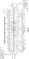
- FIG. 7 illustrates a cross-sectional partial view of an alternative embodiment of a LPCVD system 700 wherein three tumblers 706a, 706b and 706c are processed in a semi-continuous manufacturing process.
- Each tumbler reactor is loaded with graphite powders with catalysts deposited on the graphite and the tumbler reactor is inserted on one end of the LPCVD system and extracted on the opposite end of the LPCVD system after being processed through a sequence of three active zones, comprised of a heating zone 701, a reaction zone 703, and a cooling zone 705.
- the three active zones are separated from each other by two buffer zones 702 and 704 which allow the transition of each tumbler from an active zone to the next under controlled conditions of pressure and temperature.
- the tumbler 706a is heated to reach specific temperature and pressure conditions before moving to the reaction zone 703 through the buffer zone 702.
- the graphite powder contained in the tumbler reactor 706b mix with the silicon-containing process gas(es) to grow silicon nanowires on the graphite powder, before transitioning to the cooling zone 705.
- the carbon-based silicon nanowire composite powder contained in the tumbler 706c is cooled down before extracting the tumbler to unload the powder.
- This configuration ensures a semi-continuous manufacturing process where three tumblers are always present in each of the three active zones 701, 703 and 705 at any moment in time.
- the advantage of this configuration is that the reaction zone 703 is continuously growing nanowires in a tumbler with no interruption, except for the periodic transition of the tumblers from one active zone to the next.
- the configuration can be expanded to include N active zones separated from each other through N-1 buffer zones, where N is greater than 3.
- FIG. 8 illustrates a cross sectional partial view of an alternative embodiment of a LPCVD system 800 wherein the tumbler reactor comprises a helicoidal chamber 802 configured for continuous manufacturing process.
- the tumbler reactor comprises a helicoidal chamber 802 configured for continuous manufacturing process.
- a rotating helix or auger pushes the substrate powder material forward through a sequence of one or more heating zones, reaction zones and cooling zones where the injection of process gases is directed toward the reaction zones where silane is converted into silicon nanowires.
- LPCDV system 800 includes an elongated CVD chamber 802 which is comprised of at least one preheating zone 804, reaction zone 806 and cooling zone 808, and a gas manifold 801 for injecting process gases (and optionally other gases) into CVD chamber 802.
- the chamber 802 is maintained under vacuum.
- Purge gas typically nitrogen, is injected into the chamber by vacuum port 810, and an exhaust port 812 connected to a cyclone (not shown) is provided at the output end of the chamber 802 to provide the low pressure environment.
- the gas manifold 801 is comprised of an elongated gas injection member 814 that extends through the substantial or entire length of the chamber 802.
- the gas injection member 814 contains a plurality of injection ports 815 along a section of the gas injection member 814 that is positioned in the reaction zone 806.
- the injection of process gases in the reaction zone 806 (generally silane, optionally mixed with one or more inert gases such as nitrogen, argon, helium and/or hydrogen) convert silane into silicon nanowires grown on the graphite powder.
- the sections of the gas injection member 814 that are positioned in the preheating 804 and cooling zones 808 do not contain ports and thus process gases are not injected into these zones.
- Graphite powder is loaded into the chamber 802 by graphite injector 816.
- the graphite powder has been pretreated to deposit catalysts on the graphite powder.
- a rotating helix or auger 803 pushes the graphite powder forward through the preheating zone 804, reaction zone 806, and cooling zone 808.
- the auger 803 may be integrated with the gas injection member 814, or alternatively may be separate from the gas injection member 814.
- a gas conduit is formed through the center of the auger for radially distributing the gases.
- a scraper as described above can be included in one or more of the zones 804, 806, 808 to minimize buildup of powder on the inner walls of the chamber 802.
- the graphite powder As the graphite powder enters the chamber 802, the graphite powder is dried under vacuum and preheated in preheating zone 804. As the graphite powder travels through the preheating zone, the graphite is heated to a specified temperate. The heated graphite powder then exits the preheating zone and enters the reaction zone. Optionally, the preheating and reaction zones may be separated by purge or isolation curtains (not shown) or other suitable means to partially or fully isolate the zones. As the heated graphite powder enters and travels through the reaction zone 806, the graphite powder mixes with the silicon-containing process gas(es) to grow silicon nanowires on the graphite powder to form a carbon-based silicon nanowire composite powder. Next, this silicon nanowire graphite powder travels through the cooling zone 808 where the powder is cooled. Once the powder (now the formed product) passes through the cooling zone 808, the powder is removed continuously from the chamber 802 via product output 818.
- the graphite powder moves through the multiple zones by helical movement driven by the auger 803.
- Each of the zones 804, 806, 808 may require a different residence or travel time, depending on the processing step being carried out in each zone.
- preheating of the graphite powder in the preheating zone 804 may require more time than the time needed to grow the silicon nanowires in the reaction zone 806.
- control of the residence or travel time though a particular zone is achieved by varying the pitch of the auger 803 in that zone, as represented in FIG. 8 which shows three auger sections 1, 2 and 3.
- the pitch of the auger may be adjusted to be narrower or wider, depending on the need.
- the speed of travel of the graphite powder through each zone may be selectively tuned. While the three auger sections illustrated in FIG. 8 are similar in length, this is solely for simplicity and it will be understood that the length of the various auger sections may vary according to the teaching of the present invention.
- a semi-continuous batch system and process are provided, which enable multiple tumbler reactors to be processed in a semi-continuous manner.
- the process tube is elongated and configured to accommodate four tumbler reactors for example, with heating, reaction (growing) and cooling zones such that multiple tumbler reactors may undergo processing and move from zone to zone through the process tube, which allows tumblers to be loaded and unloaded at each end of the process tube in a semi-continuous manner.
- the methods, systems and reactors uses to produce the carbon-based silicon nanowire composite powders describe above, are further processed to form an anode.
- the anode is formed by coating an electrode foil with the carbon-based silicon nanowire composite powders according to coating techniques known in the art.
- the anode is further combined with a cathode, a separator and an electrolyte to form a lithium ion battery.
- the apparatus and methods described herein provide significant advantages over prior manufacturing techniques, and the increased production volume provided by the apparatus and system of the present application will help enable and promote the widespread adoption of Si nanowires grown on graphite or other carbon powders as anode materials in the battery industry.
Claims (10)
- Verfahren zum Herstellen eines kohlenstoffbasierten Silizium-Nanodraht-Verbundstoffs, das Verfahren umfassend:Bereitstellen eines kohlenstoffbasierten Substrats, das Katalysator-Nanopartikel aufweist, die auf der Oberfläche des kohlenstoffbasierten Substrats abgeschieden sind;Laden des kohlenstoffbasierten Substrats mit den darauf abgeschiedenen Katalysator-Nanopartikeln in eine Vielzahl von Tumbler-Reaktoren;Einsetzen der Vielzahl von Tumbler-Reaktoren, die das kohlenstoffbasierte Substrat mit den darauf abgeschiedenen Katalysator-Nanopartikeln enthalten, in ein Niederdruck-CVD-System, umfassend eine Abfolge von N aktiven Zonen, die durch N-1 Pufferzonen voneinander getrennt sind, die aktiven Zonen umfassend mindestens eine Heizzone, mindestens eine Reaktionszone und mindestens eine Kühlzone;Erhitzen des kohlenstoffbasierten Substrats mit den darauf abgeschiedenen Katalysator-Nanopartikeln in einem oder mehreren der Vielzahl von Tumbler-Reaktoren, die in der mindestens einen Heizzone positioniert sind, bis das kohlenstoffbasierte Substrat eine spezifische Temperatur erreicht;Züchten von Silizium-umfassenden Nanodrähten auf einem kohlenstoffbasierte Substrat aus den Katalysator-Nanopartikeln in einem oder mehreren der Vielzahl von Tumbler-Reaktoren, die in der mindestens einen Reaktionszone angeordnet sind, um einen kohlenstoffbasierten Silizium-Nanodraht-Verbundstoff durch eine Dampf-Feststoff-Synthesetechnik (VSS) zu bilden, undperiodisches Ändern der Position der Vielzahl von Tumbler-Reaktoren in dem Niederdruck-CVD-System über die Pufferzonen unter kontrollierten Druck- und Temperaturbedingungen, sodass die mindestens eine Reaktionszone kontinuierlich Silizium-umfassende Nanodrähte wachsen lässt, mit Ausnahme des periodischen Übergangs der Vielzahl von Tumbler-Reaktoren von einer aktiven Zone zur nächsten.
- Verfahren nach Anspruch 1, wobei das kohlenstoffbasierte Substrat mindestens eines von natürlichen Graphitpartikeln oder synthetischen Graphitpartikeln umfasst.
- Verfahren nach Anspruch 1, wobei die Katalysator-Nanopartikel Kupfer oder ein Kupferoxid umfassen.
- Verfahren nach Anspruch 1, wobei ein Züchten ferner Folgendes umfasst: Mischen des kohlenstoffbasierten Substrats, während ein oder mehrere Prozessgase über Einspritzöffnungen, die entlang eines Einspritzelements angeordnet sind, gleichförmig in einen oder mehrere der Vielzahl von Tumbler-Reaktoren eingespritzt werden.
- Verfahren nach Anspruch 4, wobei Temperatur und Konzentration des einen oder der mehreren Prozessgase in einem oder mehreren der Tumbler-Reaktoren durch einen Computer mit automatischer Software für die Produktion gesteuert werden.
- Verfahren nach Anspruch 4, wobei ein Mischen ferner Folgendes umfasst: Drehen des einen oder der mehreren der Vielzahl von Tumbler-Reaktoren, die in der mindestens einen Reaktionszone positioniert sind.
- Verfahren nach Anspruch 4, wobei das eine oder die mehreren Prozessgase einen Silizium-umfassenden Vorläufer umfassen und die Umwandlung des Silizium-umfassenden Vorläufers in Silizium-Nanodrähte mehr als 90 % ist.
- Verfahren nach Anspruch 1, wobei das Laden ferner Folgendes umfasst: Laden einer Gewichtsmenge von mehr als 10 kg des kohlenstoffbasierten Substrats mit den darauf abgeschiedenen Katalysator-Nanopartikeln in jeden der Vielzahl von Tumbler-Reaktoren.
- Verfahren nach Anspruch 1, wobei das Laden ferner Folgendes umfasst: Laden einer Gewichtsmenge von mehr als 100 kg des kohlenstoffbasierten Substrats mit den darauf abgeschiedenen Katalysator-Nanopartikeln in jeden der Vielzahl von Tumbler-Reaktoren.
- Verfahren nach Anspruch 1, ferner umfassend: Abstreifen der Innenwände von einem oder mehreren der Tumbler-Reaktoren in der Niederdruck-CVD-Anlage, um den Aufbau von kohlenstoffbasiertem Substrat an den Innenwänden zu minimieren.
Priority Applications (1)
| Application Number | Priority Date | Filing Date | Title |
|---|---|---|---|
| PL20195843T PL3778471T3 (pl) | 2016-07-15 | 2017-07-14 | Sposób wytwarzania nanodrutów krzemowych na proszkach węglowych do stosowania w bateriach |
Applications Claiming Priority (3)
| Application Number | Priority Date | Filing Date | Title |
|---|---|---|---|
| US201662363087P | 2016-07-15 | 2016-07-15 | |
| PCT/US2017/042246 WO2018013991A2 (en) | 2016-07-15 | 2017-07-14 | Manufacturing apparatus and method for making silicon nanowires on carbon based powders for use in batteries |
| EP17828578.9A EP3484810B1 (de) | 2016-07-15 | 2017-07-14 | Verfahren und vorrichtung zur herstellung von siliciumnanodrähten auf kohlenstoffbasierten pulvern zur verwendung in batterien |
Related Parent Applications (2)
| Application Number | Title | Priority Date | Filing Date |
|---|---|---|---|
| EP17828578.9A Division EP3484810B1 (de) | 2016-07-15 | 2017-07-14 | Verfahren und vorrichtung zur herstellung von siliciumnanodrähten auf kohlenstoffbasierten pulvern zur verwendung in batterien |
| EP17828578.9A Division-Into EP3484810B1 (de) | 2016-07-15 | 2017-07-14 | Verfahren und vorrichtung zur herstellung von siliciumnanodrähten auf kohlenstoffbasierten pulvern zur verwendung in batterien |
Publications (2)
| Publication Number | Publication Date |
|---|---|
| EP3778471A1 EP3778471A1 (de) | 2021-02-17 |
| EP3778471B1 true EP3778471B1 (de) | 2022-04-20 |
Family
ID=60940785
Family Applications (4)
| Application Number | Title | Priority Date | Filing Date |
|---|---|---|---|
| EP23195245.8A Pending EP4292702A3 (de) | 2016-07-15 | 2017-07-14 | Verfahren und vorrichtung zur herstellung von siliciumnanodrähten auf kohlenstoffbasierten pulvern zur verwendung in batterien |
| EP23195238.3A Pending EP4273296A1 (de) | 2016-07-15 | 2017-07-14 | Verfahren und vorrichtung zur herstellung von siliciumnanodrähten auf kohlenstoffbasierten pulvern zur verwendung in batterien |
| EP17828578.9A Active EP3484810B1 (de) | 2016-07-15 | 2017-07-14 | Verfahren und vorrichtung zur herstellung von siliciumnanodrähten auf kohlenstoffbasierten pulvern zur verwendung in batterien |
| EP20195843.6A Active EP3778471B1 (de) | 2016-07-15 | 2017-07-14 | Herstellungsverfahren von siliciumnanodrähten auf kohlenstoffbasierten pulvern zur verwendung in batterien |
Family Applications Before (3)
| Application Number | Title | Priority Date | Filing Date |
|---|---|---|---|
| EP23195245.8A Pending EP4292702A3 (de) | 2016-07-15 | 2017-07-14 | Verfahren und vorrichtung zur herstellung von siliciumnanodrähten auf kohlenstoffbasierten pulvern zur verwendung in batterien |
| EP23195238.3A Pending EP4273296A1 (de) | 2016-07-15 | 2017-07-14 | Verfahren und vorrichtung zur herstellung von siliciumnanodrähten auf kohlenstoffbasierten pulvern zur verwendung in batterien |
| EP17828578.9A Active EP3484810B1 (de) | 2016-07-15 | 2017-07-14 | Verfahren und vorrichtung zur herstellung von siliciumnanodrähten auf kohlenstoffbasierten pulvern zur verwendung in batterien |
Country Status (11)
| Country | Link |
|---|---|
| US (3) | US11728477B2 (de) |
| EP (4) | EP4292702A3 (de) |
| JP (2) | JP7155104B2 (de) |
| KR (1) | KR102531225B1 (de) |
| CN (1) | CN109689567B (de) |
| DK (2) | DK3778471T3 (de) |
| ES (2) | ES2913682T3 (de) |
| FI (1) | FI3484810T3 (de) |
| HU (2) | HUE064985T2 (de) |
| PL (2) | PL3778471T3 (de) |
| WO (1) | WO2018013991A2 (de) |
Families Citing this family (13)
| Publication number | Priority date | Publication date | Assignee | Title |
|---|---|---|---|---|
| CN106936677B (zh) * | 2015-12-31 | 2020-06-26 | 华为技术有限公司 | 一种模块化ups系统及功率设备的数据传输方法 |
| ES2913682T3 (es) | 2016-07-15 | 2022-06-03 | Oned Mat Inc | Procedimiento de fabricación para la fabricación de nanocables de silicio en polvos a base de carbono para su uso en baterías |
| US11174552B2 (en) * | 2018-06-12 | 2021-11-16 | Applied Materials, Inc. | Rotary reactor for uniform particle coating with thin films |
| US11641012B2 (en) | 2019-01-14 | 2023-05-02 | Global Graphene Group, Inc. | Process for producing graphene/silicon nanowire hybrid material for a lithium-ion battery |
| KR20200100928A (ko) * | 2019-02-19 | 2020-08-27 | 현대자동차주식회사 | 분말의 표면 처리 장치 및 이를 이용한 분말의 표면 처리 방법 |
| TWI765795B (zh) | 2019-04-24 | 2022-05-21 | 美商應用材料股份有限公司 | 具有旋轉葉片與氣體注入之用於在固定腔室中塗覆粒子的反應器 |
| BR112022003964A2 (pt) | 2019-09-03 | 2022-05-24 | Haldor Topsoe As | Forno reformador com tubos reformadores suportados |
| CN110592559B (zh) * | 2019-09-17 | 2021-08-27 | 淮北摩兰科技有限公司 | 一种显示屏线路保护装置及方法 |
| CN110641028B (zh) * | 2019-09-25 | 2021-05-04 | 大同新成新材料股份有限公司 | 碳毡加工生产用翻转式热压机及其使用方法 |
| EP3822395A1 (de) * | 2019-11-13 | 2021-05-19 | Fundación Imdea Materiales | Nanodrahtnetzwerk |
| CN112599758B (zh) * | 2021-03-03 | 2021-07-06 | 拓米(成都)应用技术研究院有限公司 | 纳米硅团聚体复合负极材料及其制备方法 |
| CN117396428A (zh) | 2021-05-28 | 2024-01-12 | 恩维雷斯公司 | 用于制备硅-碳复合材料的方法 |
| US20230307613A1 (en) * | 2021-12-23 | 2023-09-28 | Oned Material, Inc. | Novel composites for anode electrodes |
Family Cites Families (85)
| Publication number | Priority date | Publication date | Assignee | Title |
|---|---|---|---|---|
| US3395674A (en) * | 1963-09-23 | 1968-08-06 | Int Resistance Co | Apparatus for vapor coating tumbling substrates |
| US4136216A (en) | 1975-08-26 | 1979-01-23 | Surface Technology, Inc. | Non-precious metal colloidal dispersions for electroless metal deposition |
| JPS5268886A (en) * | 1975-12-08 | 1977-06-08 | Fujitsu Ltd | Surface treatment method of powder |
| US4171225A (en) | 1976-01-23 | 1979-10-16 | U.S. Philips Corporation | Electroless copper plating solutions |
| US4400436A (en) | 1980-06-30 | 1983-08-23 | Ppg Industries, Inc. | Direct electroless deposition of cuprous oxide films |
| JPS58136701A (ja) | 1982-02-08 | 1983-08-13 | Japan Synthetic Rubber Co Ltd | 微粒子のコーティング方法 |
| DE3328709A1 (de) | 1983-08-09 | 1985-02-28 | Bayer Ag, 5090 Leverkusen | Drehrohrofen und dessen verwendung |
| JPS6142362U (ja) | 1985-07-18 | 1986-03-18 | 日本精工株式会社 | 緊急ロツク解除機構付シ−トベルト巻取装置 |
| JPS6345834U (de) | 1986-09-12 | 1988-03-28 | ||
| US5897945A (en) | 1996-02-26 | 1999-04-27 | President And Fellows Of Harvard College | Metal oxide nanorods |
| US6036774A (en) | 1996-02-26 | 2000-03-14 | President And Fellows Of Harvard College | Method of producing metal oxide nanorods |
| US5677082A (en) | 1996-05-29 | 1997-10-14 | Ucar Carbon Technology Corporation | Compacted carbon for electrochemical cells |
| US5997832A (en) | 1997-03-07 | 1999-12-07 | President And Fellows Of Harvard College | Preparation of carbide nanorods |
| US6479030B1 (en) | 1997-09-16 | 2002-11-12 | Inorganic Specialists, Inc. | Carbon electrode material |
| US6303266B1 (en) | 1998-09-24 | 2001-10-16 | Kabushiki Kaisha Toshiba | Resin useful for resist, resist composition and pattern forming process using the same |
| FR2786208B1 (fr) * | 1998-11-25 | 2001-02-09 | Centre Nat Rech Scient | Procede de croissance cristalline sur substrat et reacteur pour sa mise en oeuvre |
| US6225198B1 (en) | 2000-02-04 | 2001-05-01 | The Regents Of The University Of California | Process for forming shaped group II-VI semiconductor nanocrystals, and product formed using process |
| US6306736B1 (en) | 2000-02-04 | 2001-10-23 | The Regents Of The University Of California | Process for forming shaped group III-V semiconductor nanocrystals, and product formed using process |
| US6326056B1 (en) * | 2000-02-16 | 2001-12-04 | Specialty Coating Systems, Inc. | Mobile cellular tumble coating method |
| EP1136587B1 (de) * | 2000-03-23 | 2013-05-15 | Hitachi Metals, Ltd. | Vorrichtung zum Auftragen von Filmen |
| KR100995457B1 (ko) | 2000-08-22 | 2010-11-18 | 프레지던트 앤드 펠로우즈 오브 하버드 칼리지 | 나노센서 제조 방법 |
| US7301199B2 (en) | 2000-08-22 | 2007-11-27 | President And Fellows Of Harvard College | Nanoscale wires and related devices |
| JP2002060943A (ja) | 2000-08-22 | 2002-02-28 | Tohoku Electric Power Co Inc | 高純度シリコンの被覆方法及び装置 |
| NO20010929D0 (no) * | 2001-02-23 | 2001-02-23 | Norsk Hydro As | FremgangsmÕte for utøvelse av termiske reaksjoner mellom reaktanter samt en ovn for samme |
| KR100394080B1 (ko) * | 2001-03-20 | 2003-08-06 | 광주과학기술원 | 표면 개질된 실리카와 그 제조방법 및 장치 |
| KR101008294B1 (ko) | 2001-03-30 | 2011-01-13 | 더 리전트 오브 더 유니버시티 오브 캘리포니아 | 나노구조체 및 나노와이어의 제조 방법 및 그로부터 제조되는 디바이스 |
| JP4388717B2 (ja) * | 2001-06-27 | 2009-12-24 | 株式会社ユーテック | Cvd成膜装置及びcvd成膜方法 |
| US20040026684A1 (en) | 2002-04-02 | 2004-02-12 | Nanosys, Inc. | Nanowire heterostructures for encoding information |
| US6872645B2 (en) | 2002-04-02 | 2005-03-29 | Nanosys, Inc. | Methods of positioning and/or orienting nanostructures |
| US20040037767A1 (en) | 2002-08-21 | 2004-02-26 | First Nano, Inc. | Method and apparatus of carbon nanotube fabrication |
| US7067867B2 (en) | 2002-09-30 | 2006-06-27 | Nanosys, Inc. | Large-area nonenabled macroelectronic substrates and uses therefor |
| CN1150997C (zh) | 2002-12-27 | 2004-05-26 | 浙江大学 | 在碳纳米管表面负载纳米单金属粒子的方法 |
| EP1445236A1 (de) | 2003-02-05 | 2004-08-11 | Université de Liège | Verfahren und Vorrichtung zur Herstellung von Kohlenstoffnanoröhren |
| JP4274414B2 (ja) * | 2003-05-21 | 2009-06-10 | 富士機械製造株式会社 | 球状半導体素子の製造方法及び製造装置 |
| US7261779B2 (en) * | 2003-06-05 | 2007-08-28 | Lockheed Martin Corporation | System, method, and apparatus for continuous synthesis of single-walled carbon nanotubes |
| CN1249276C (zh) | 2003-07-11 | 2006-04-05 | 华中师范大学 | 化学沉淀法制备稳定的纳米氧化亚铜晶须的方法 |
| KR100771393B1 (ko) | 2003-10-20 | 2007-10-30 | 하리마 카세이 가부시키가이샤 | 건조 분말상의 금속 미립자 및 금속 산화물 미립자와 그용도 |
| US20110039690A1 (en) | 2004-02-02 | 2011-02-17 | Nanosys, Inc. | Porous substrates, articles, systems and compositions comprising nanofibers and methods of their use and production |
| US7553371B2 (en) | 2004-02-02 | 2009-06-30 | Nanosys, Inc. | Porous substrates, articles, systems and compositions comprising nanofibers and methods of their use and production |
| US7105428B2 (en) | 2004-04-30 | 2006-09-12 | Nanosys, Inc. | Systems and methods for nanowire growth and harvesting |
| EP1829141B1 (de) | 2004-12-09 | 2013-05-29 | Nanosys, Inc. | Auf nanodrähten basierende membranelektrodenbaugruppen für brennstoffzellen |
| US7842432B2 (en) | 2004-12-09 | 2010-11-30 | Nanosys, Inc. | Nanowire structures comprising carbon |
| JP2008540309A (ja) | 2005-05-12 | 2008-11-20 | ベリー スモール パーティクル コンパニー ピーティーワイ リミテッド | 材料の製造方法 |
| CN101292365B (zh) | 2005-06-17 | 2012-04-04 | 依路米尼克斯公司 | 纳米结构的光伏器件及其制造方法 |
| EP1952467B9 (de) | 2005-11-21 | 2012-03-14 | Nanosys, Inc. | Nanodraht-strukturen mit kohlenstoff |
| KR100778011B1 (ko) | 2005-12-06 | 2007-11-28 | 한국과학기술원 | 자기조립 초분자체를 이용한 금속 나노와이어 어레이의제조방법 |
| JP2009522197A (ja) | 2005-12-29 | 2009-06-11 | ナノシス・インコーポレイテッド | パターン形成された基板上のナノワイヤの配向した成長のための方法 |
| CN100463111C (zh) | 2006-01-14 | 2009-02-18 | 清华大学 | 硅线的制备方法 |
| JP2008019461A (ja) | 2006-07-11 | 2008-01-31 | Fujifilm Corp | 金属ナノ粒子の製造方法、金属ナノ粒子及び金属ナノ粒子分散物 |
| KR100783667B1 (ko) * | 2006-08-10 | 2007-12-07 | 한국화학연구원 | 입자형 다결정 실리콘의 제조방법 및 제조장치 |
| JP2010509171A (ja) | 2006-11-07 | 2010-03-25 | ナノシス・インク. | ナノワイヤー成長用システム及び方法 |
| US20080135089A1 (en) | 2006-11-15 | 2008-06-12 | General Electric Company | Graded hybrid amorphous silicon nanowire solar cells |
| KR100824301B1 (ko) * | 2006-12-21 | 2008-04-22 | 세메스 주식회사 | 반응 챔버와 이를 포함하는 탄소나노튜브 합성 장치 및 설비 |
| CN100448798C (zh) | 2007-04-29 | 2009-01-07 | 北京科技大学 | 一种制备碳化硅晶须增强碳化硅复合材料零件的方法 |
| GB0713898D0 (en) | 2007-07-17 | 2007-08-29 | Nexeon Ltd | A method of fabricating structured particles composed of silcon or a silicon-based material and their use in lithium rechargeable batteries |
| WO2009021988A1 (fr) | 2007-08-14 | 2009-02-19 | Universite Libre De Bruxelles | Procédé de dépôt de nanoparticules sur un support |
| US20090186276A1 (en) | 2008-01-18 | 2009-07-23 | Aruna Zhamu | Hybrid nano-filament cathode compositions for lithium metal or lithium ion batteries |
| US20110308463A1 (en) | 2008-05-30 | 2011-12-22 | Alta Devices, Inc. | Chemical vapor deposition reactor with isolated sequential processing zones |
| CN102119120B (zh) * | 2008-08-08 | 2013-08-07 | 株式会社东芝 | 纳米碳生成装置 |
| KR101073853B1 (ko) | 2008-12-29 | 2011-10-17 | 도레이첨단소재 주식회사 | 기재 상에 나노 구조체로 이루어진 망상 필름의 제조 방법 및 그에 따라 제조된 나노 구조체 망상 필름이 구비된 기재 |
| FR2944783B1 (fr) | 2009-04-28 | 2011-06-03 | Commissariat Energie Atomique | Procede d'elaboration de nanofils de silicium et/ou de germanium. |
| JP5686988B2 (ja) | 2009-05-04 | 2015-03-18 | シャープ株式会社 | 燃料電池用膜電極複合体に用いられる触媒層、それを用いる燃料電池用膜電極複合体、燃料電池、およびその製造方法 |
| US20100285358A1 (en) | 2009-05-07 | 2010-11-11 | Amprius, Inc. | Electrode Including Nanostructures for Rechargeable Cells |
| DK3859830T3 (da) | 2009-05-19 | 2022-04-11 | Oned Mat Inc | Nanostrukturerede materialer til batterianvendelser |
| EP2440323B1 (de) * | 2009-06-09 | 2019-08-28 | Haydale Graphene Industries plc | Verfahren und vorrichtung zur partikelverarbeitung mit plasma |
| US8623288B1 (en) | 2009-06-29 | 2014-01-07 | Nanosys, Inc. | Apparatus and methods for high density nanowire growth |
| CN101604753A (zh) | 2009-07-24 | 2009-12-16 | 成都中科来方能源科技有限公司 | 碳硅复合材料及其制备方法和用途 |
| US9138965B2 (en) | 2009-10-30 | 2015-09-22 | The Board Of Trustees Of The Leland Stanford Junior University | Conductive fibrous materials |
| WO2011060024A2 (en) | 2009-11-11 | 2011-05-19 | Amprius, Inc. | Open structures in substrates for electrodes |
| CN101791538A (zh) | 2010-03-17 | 2010-08-04 | 上海大学 | 用负载氧化铜介孔碳材料去除水溶液中酚的方法 |
| KR101128928B1 (ko) * | 2010-10-26 | 2012-03-27 | 주식회사 지오스 | 열화학 기상 증착법을 이용한 탄소나노튜브 대량 합성장치 |
| CA2819999C (en) * | 2010-12-08 | 2018-09-04 | Innovative Carbon Limited | Particulate materials, composites comprising them, preparation and uses thereof |
| WO2013016339A2 (en) | 2011-07-26 | 2013-01-31 | Nanosys, Inc. | Nanostructured battery active materials and methods of producing same |
| KR20130037091A (ko) | 2011-10-05 | 2013-04-15 | 삼성에스디아이 주식회사 | 음극 활물질 및 이를 채용한 리튬 전지 |
| CN102530931B (zh) | 2011-12-14 | 2014-04-02 | 天津大学 | 基于石墨烯的纳米复合材料及其制备方法 |
| US8865057B2 (en) | 2012-02-06 | 2014-10-21 | Wisconsin Alumni Research Foundation | Apparatus and methods for industrial-scale production of metal matrix nanocomposites |
| US9711787B2 (en) | 2012-11-30 | 2017-07-18 | Lg Chem, Ltd. | Anode active material for lithium secondary battery, preparation method thereof, and lithium secondary battery comprising the same |
| KR101557559B1 (ko) | 2012-11-30 | 2015-10-07 | 주식회사 엘지화학 | 리튬 이차 전지용 음극재, 이의 제조 방법 및 이를 포함하는 리튬 이차 전지 |
| US9676627B2 (en) | 2014-05-14 | 2017-06-13 | University Of Dayton | Growth of silicon and boron nitride nanomaterials on carbon fibers by chemical vapor deposition |
| KR101637980B1 (ko) * | 2014-09-24 | 2016-07-08 | 울산과학기술원 | 열 화학기상증착 장치 및 열 화학기상증착 방법 |
| JP6312212B2 (ja) * | 2014-11-18 | 2018-04-18 | 信越化学工業株式会社 | 回転式筒状炉、及び非水電解質二次電池用負極活物質の製造方法 |
| JP6312213B2 (ja) * | 2014-11-18 | 2018-04-18 | 信越化学工業株式会社 | 回転式筒状炉、及び非水電解質二次電池用負極活物質の製造方法 |
| US10516169B2 (en) * | 2015-11-12 | 2019-12-24 | Sonata Scientific LLC | Apparatus and method for coating bulk quantities of solid particles |
| ES2913682T3 (es) | 2016-07-15 | 2022-06-03 | Oned Mat Inc | Procedimiento de fabricación para la fabricación de nanocables de silicio en polvos a base de carbono para su uso en baterías |
| US11174552B2 (en) * | 2018-06-12 | 2021-11-16 | Applied Materials, Inc. | Rotary reactor for uniform particle coating with thin films |
-
2017
- 2017-07-14 ES ES20195843T patent/ES2913682T3/es active Active
- 2017-07-14 FI FIEP17828578.9T patent/FI3484810T3/fi active
- 2017-07-14 HU HUE17828578A patent/HUE064985T2/hu unknown
- 2017-07-14 EP EP23195245.8A patent/EP4292702A3/de active Pending
- 2017-07-14 JP JP2019502003A patent/JP7155104B2/ja active Active
- 2017-07-14 CN CN201780056498.5A patent/CN109689567B/zh active Active
- 2017-07-14 EP EP23195238.3A patent/EP4273296A1/de active Pending
- 2017-07-14 PL PL20195843T patent/PL3778471T3/pl unknown
- 2017-07-14 HU HUE20195843A patent/HUE058982T2/hu unknown
- 2017-07-14 DK DK20195843.6T patent/DK3778471T3/da active
- 2017-07-14 KR KR1020197004648A patent/KR102531225B1/ko active IP Right Grant
- 2017-07-14 DK DK17828578.9T patent/DK3484810T3/da active
- 2017-07-14 ES ES17828578T patent/ES2962317T3/es active Active
- 2017-07-14 WO PCT/US2017/042246 patent/WO2018013991A2/en unknown
- 2017-07-14 EP EP17828578.9A patent/EP3484810B1/de active Active
- 2017-07-14 PL PL17828578.9T patent/PL3484810T3/pl unknown
- 2017-07-14 EP EP20195843.6A patent/EP3778471B1/de active Active
- 2017-07-14 US US15/650,797 patent/US11728477B2/en active Active
- 2017-07-14 US US15/650,775 patent/US10862114B2/en active Active
-
2022
- 2022-10-04 JP JP2022160349A patent/JP2022189833A/ja active Pending
-
2023
- 2023-07-10 US US18/220,171 patent/US20230352668A1/en active Pending
Also Published As
| Publication number | Publication date |
|---|---|
| KR102531225B1 (ko) | 2023-05-10 |
| HUE064985T2 (hu) | 2024-04-28 |
| CN109689567B (zh) | 2022-09-09 |
| DK3484810T3 (da) | 2023-11-20 |
| EP4292702A3 (de) | 2024-04-17 |
| FI3484810T3 (fi) | 2023-11-09 |
| JP7155104B2 (ja) | 2022-10-18 |
| EP4273296A1 (de) | 2023-11-08 |
| EP3484810A4 (de) | 2020-03-25 |
| US20230352668A1 (en) | 2023-11-02 |
| HUE058982T2 (hu) | 2022-10-28 |
| KR20190030723A (ko) | 2019-03-22 |
| US10862114B2 (en) | 2020-12-08 |
| WO2018013991A2 (en) | 2018-01-18 |
| PL3484810T3 (pl) | 2024-02-19 |
| ES2913682T3 (es) | 2022-06-03 |
| EP3484810A2 (de) | 2019-05-22 |
| US20180019467A1 (en) | 2018-01-18 |
| PL3778471T3 (pl) | 2022-06-13 |
| JP2022189833A (ja) | 2022-12-22 |
| ES2962317T3 (es) | 2024-03-18 |
| EP3778471A1 (de) | 2021-02-17 |
| DK3778471T3 (da) | 2022-05-23 |
| US20180019468A1 (en) | 2018-01-18 |
| US11728477B2 (en) | 2023-08-15 |
| CN109689567A (zh) | 2019-04-26 |
| EP4292702A2 (de) | 2023-12-20 |
| WO2018013991A3 (en) | 2018-02-22 |
| EP3484810B1 (de) | 2023-10-11 |
| JP2019527187A (ja) | 2019-09-26 |
Similar Documents
| Publication | Publication Date | Title |
|---|---|---|
| US20230352668A1 (en) | Manufacturing apparatus and method for making silicon nanowires on carbon based powders for use in batteries | |
| Hu et al. | High performance germanium-based anode materials | |
| Wu et al. | Designing nanostructured Si anodes for high energy lithium ion batteries | |
| Zhu et al. | Achieving high-performance silicon anodes of lithium-ion batteries via atomic and molecular layer deposited surface coatings: An overview | |
| Weng et al. | Electrodeposited silicon nanowires from silica dissolved in molten salts as a binder-free anode for lithium-ion batteries | |
| JP5965040B2 (ja) | 非水電解質二次電池用負極活物質の製造方法 | |
| JP2018519648A (ja) | 非水電解質二次電池用負極材、その製造方法、及びこれを含む非水電解質二次電池 | |
| US8920970B2 (en) | Anode materials for lithium-ion batteries | |
| Zhao et al. | Nanostructured electrode materials for rechargeable lithium-ion batteries | |
| KR20160065107A (ko) | 규소 함유 재료, 비수전해질 이차 전지용 부극, 비수전해질 이차 전지 및 그들의 제조 방법 | |
| Jaramillo-Cabanzo et al. | One-dimensional nanomaterials in lithium-ion batteries | |
| US20220052323A1 (en) | Synthesis of graphitic shells on silicon nanoparticles | |
| US20240162426A1 (en) | Manufacturing apparatus and method for making silicon nanowires on carbon based powders for use in batteries | |
| KR102610381B1 (ko) | 탄소나노튜브 복합체를 포함하는 리튬이차전지용 음극재 제조방법 및 이를 위한 제조장치 | |
| US20220246932A1 (en) | Electrode, electrical energy storage device & method | |
| JP2015218080A (ja) | 粒状珪素酸化物及びその製造方法 |
Legal Events
| Date | Code | Title | Description |
|---|---|---|---|
| PUAI | Public reference made under article 153(3) epc to a published international application that has entered the european phase |
Free format text: ORIGINAL CODE: 0009012 |
|
| STAA | Information on the status of an ep patent application or granted ep patent |
Free format text: STATUS: THE APPLICATION HAS BEEN PUBLISHED |
|
| AC | Divisional application: reference to earlier application |
Ref document number: 3484810 Country of ref document: EP Kind code of ref document: P |
|
| AK | Designated contracting states |
Kind code of ref document: A1 Designated state(s): AL AT BE BG CH CY CZ DE DK EE ES FI FR GB GR HR HU IE IS IT LI LT LU LV MC MK MT NL NO PL PT RO RS SE SI SK SM TR |
|
| STAA | Information on the status of an ep patent application or granted ep patent |
Free format text: STATUS: REQUEST FOR EXAMINATION WAS MADE |
|
| 17P | Request for examination filed |
Effective date: 20210811 |
|
| RBV | Designated contracting states (corrected) |
Designated state(s): AL AT BE BG CH CY CZ DE DK EE ES FI FR GB GR HR HU IE IS IT LI LT LU LV MC MK MT NL NO PL PT RO RS SE SI SK SM TR |
|
| RIC1 | Information provided on ipc code assigned before grant |
Ipc: H01M 4/90 20060101ALN20211104BHEP Ipc: H01M 4/583 20100101ALN20211104BHEP Ipc: H01M 4/62 20060101ALN20211104BHEP Ipc: H01M 4/38 20060101ALN20211104BHEP Ipc: H01M 4/36 20060101ALN20211104BHEP Ipc: H01M 10/0525 20100101ALN20211104BHEP Ipc: B01J 4/00 20060101ALI20211104BHEP Ipc: B01J 3/00 20060101ALI20211104BHEP Ipc: B01J 19/28 20060101ALI20211104BHEP Ipc: B01J 15/00 20060101ALI20211104BHEP Ipc: C23C 16/54 20060101ALI20211104BHEP Ipc: B01J 19/00 20060101ALI20211104BHEP Ipc: C22C 38/02 20060101ALI20211104BHEP Ipc: H01M 4/88 20060101ALI20211104BHEP Ipc: H01J 37/32 20060101ALI20211104BHEP Ipc: C23C 16/455 20060101ALI20211104BHEP Ipc: C23C 16/44 20060101ALI20211104BHEP Ipc: C23C 16/24 20060101ALI20211104BHEP Ipc: C23C 16/22 20060101ALI20211104BHEP Ipc: C01B 33/029 20060101ALI20211104BHEP Ipc: C01B 33/021 20060101ALI20211104BHEP Ipc: C01B 33/023 20060101ALI20211104BHEP Ipc: C01B 33/027 20060101ALI20211104BHEP Ipc: C01B 33/02 20060101ALI20211104BHEP Ipc: B82Y 30/00 20110101ALI20211104BHEP Ipc: B82Y 99/00 20110101ALI20211104BHEP Ipc: B82Y 40/00 20110101AFI20211104BHEP |
|
| REG | Reference to a national code |
Ref country code: DE Ref legal event code: R079 Ref document number: 602017056431 Country of ref document: DE Free format text: PREVIOUS MAIN CLASS: B82Y0040000000 Ipc: C23C0016240000 |
|
| GRAP | Despatch of communication of intention to grant a patent |
Free format text: ORIGINAL CODE: EPIDOSNIGR1 |
|
| STAA | Information on the status of an ep patent application or granted ep patent |
Free format text: STATUS: GRANT OF PATENT IS INTENDED |
|
| RIC1 | Information provided on ipc code assigned before grant |
Ipc: H01M 4/90 20060101ALN20211201BHEP Ipc: H01M 4/583 20100101ALN20211201BHEP Ipc: H01M 4/62 20060101ALN20211201BHEP Ipc: H01M 4/38 20060101ALN20211201BHEP Ipc: H01M 4/36 20060101ALN20211201BHEP Ipc: H01M 10/0525 20100101ALN20211201BHEP Ipc: B01J 19/28 20060101ALI20211201BHEP Ipc: B01J 15/00 20060101ALI20211201BHEP Ipc: B01J 4/00 20060101ALI20211201BHEP Ipc: B82Y 30/00 20110101ALI20211201BHEP Ipc: B82Y 99/00 20110101ALI20211201BHEP Ipc: B82Y 40/00 20110101ALI20211201BHEP Ipc: B01J 3/00 20060101ALI20211201BHEP Ipc: H01M 4/88 20060101ALI20211201BHEP Ipc: H01J 37/32 20060101ALI20211201BHEP Ipc: C22C 38/02 20060101ALI20211201BHEP Ipc: C23C 16/54 20060101ALI20211201BHEP Ipc: C23C 16/455 20060101ALI20211201BHEP Ipc: C23C 16/44 20060101ALI20211201BHEP Ipc: C23C 16/24 20060101AFI20211201BHEP |
|
| INTG | Intention to grant announced |
Effective date: 20211223 |
|
| RIC1 | Information provided on ipc code assigned before grant |
Ipc: H01M 10/0525 20100101ALN20211213BHEP Ipc: H01M 4/90 20060101ALN20211213BHEP Ipc: H01M 4/62 20060101ALN20211213BHEP Ipc: H01M 4/583 20100101ALN20211213BHEP Ipc: H01M 4/38 20060101ALN20211213BHEP Ipc: H01M 4/36 20060101ALN20211213BHEP Ipc: B01J 19/28 20060101ALI20211213BHEP Ipc: B01J 15/00 20060101ALI20211213BHEP Ipc: B01J 4/00 20060101ALI20211213BHEP Ipc: B01J 3/00 20060101ALI20211213BHEP Ipc: H01M 4/88 20060101ALI20211213BHEP Ipc: H01J 37/32 20060101ALI20211213BHEP Ipc: C22C 38/02 20060101ALI20211213BHEP Ipc: C23C 16/54 20060101ALI20211213BHEP Ipc: C23C 16/455 20060101ALI20211213BHEP Ipc: C23C 16/44 20060101ALI20211213BHEP Ipc: C23C 16/24 20060101AFI20211213BHEP |
|
| GRAS | Grant fee paid |
Free format text: ORIGINAL CODE: EPIDOSNIGR3 |
|
| GRAA | (expected) grant |
Free format text: ORIGINAL CODE: 0009210 |
|
| STAA | Information on the status of an ep patent application or granted ep patent |
Free format text: STATUS: THE PATENT HAS BEEN GRANTED |
|
| AC | Divisional application: reference to earlier application |
Ref document number: 3484810 Country of ref document: EP Kind code of ref document: P |
|
| AK | Designated contracting states |
Kind code of ref document: B1 Designated state(s): AL AT BE BG CH CY CZ DE DK EE ES FI FR GB GR HR HU IE IS IT LI LT LU LV MC MK MT NL NO PL PT RO RS SE SI SK SM TR |
|
| REG | Reference to a national code |
Ref country code: GB Ref legal event code: FG4D |
|
| REG | Reference to a national code |
Ref country code: CH Ref legal event code: EP |
|
| REG | Reference to a national code |
Ref country code: IE Ref legal event code: FG4D |
|
| REG | Reference to a national code |
Ref country code: FI Ref legal event code: FGE Ref country code: DE Ref legal event code: R096 Ref document number: 602017056431 Country of ref document: DE |
|
| REG | Reference to a national code |
Ref country code: AT Ref legal event code: REF Ref document number: 1485202 Country of ref document: AT Kind code of ref document: T Effective date: 20220515 |
|
| REG | Reference to a national code |
Ref country code: DK Ref legal event code: T3 Effective date: 20220518 |
|
| REG | Reference to a national code |
Ref country code: NL Ref legal event code: FP |
|
| REG | Reference to a national code |
Ref country code: SE Ref legal event code: TRGR |
|
| REG | Reference to a national code |
Ref country code: ES Ref legal event code: FG2A Ref document number: 2913682 Country of ref document: ES Kind code of ref document: T3 Effective date: 20220603 |
|
| REG | Reference to a national code |
Ref country code: NO Ref legal event code: T2 Effective date: 20220420 |
|
| REG | Reference to a national code |
Ref country code: LT Ref legal event code: MG9D |
|
| REG | Reference to a national code |
Ref country code: HU Ref legal event code: AG4A Ref document number: E058982 Country of ref document: HU |
|
| PG25 | Lapsed in a contracting state [announced via postgrant information from national office to epo] |
Ref country code: PT Free format text: LAPSE BECAUSE OF FAILURE TO SUBMIT A TRANSLATION OF THE DESCRIPTION OR TO PAY THE FEE WITHIN THE PRESCRIBED TIME-LIMIT Effective date: 20220822 Ref country code: LT Free format text: LAPSE BECAUSE OF FAILURE TO SUBMIT A TRANSLATION OF THE DESCRIPTION OR TO PAY THE FEE WITHIN THE PRESCRIBED TIME-LIMIT Effective date: 20220420 Ref country code: HR Free format text: LAPSE BECAUSE OF FAILURE TO SUBMIT A TRANSLATION OF THE DESCRIPTION OR TO PAY THE FEE WITHIN THE PRESCRIBED TIME-LIMIT Effective date: 20220420 Ref country code: GR Free format text: LAPSE BECAUSE OF FAILURE TO SUBMIT A TRANSLATION OF THE DESCRIPTION OR TO PAY THE FEE WITHIN THE PRESCRIBED TIME-LIMIT Effective date: 20220721 Ref country code: BG Free format text: LAPSE BECAUSE OF FAILURE TO SUBMIT A TRANSLATION OF THE DESCRIPTION OR TO PAY THE FEE WITHIN THE PRESCRIBED TIME-LIMIT Effective date: 20220720 |
|
| PG25 | Lapsed in a contracting state [announced via postgrant information from national office to epo] |
Ref country code: RS Free format text: LAPSE BECAUSE OF FAILURE TO SUBMIT A TRANSLATION OF THE DESCRIPTION OR TO PAY THE FEE WITHIN THE PRESCRIBED TIME-LIMIT Effective date: 20220420 Ref country code: LV Free format text: LAPSE BECAUSE OF FAILURE TO SUBMIT A TRANSLATION OF THE DESCRIPTION OR TO PAY THE FEE WITHIN THE PRESCRIBED TIME-LIMIT Effective date: 20220420 Ref country code: IS Free format text: LAPSE BECAUSE OF FAILURE TO SUBMIT A TRANSLATION OF THE DESCRIPTION OR TO PAY THE FEE WITHIN THE PRESCRIBED TIME-LIMIT Effective date: 20220820 |
|
| REG | Reference to a national code |
Ref country code: DE Ref legal event code: R097 Ref document number: 602017056431 Country of ref document: DE |
|
| PG25 | Lapsed in a contracting state [announced via postgrant information from national office to epo] |
Ref country code: SM Free format text: LAPSE BECAUSE OF FAILURE TO SUBMIT A TRANSLATION OF THE DESCRIPTION OR TO PAY THE FEE WITHIN THE PRESCRIBED TIME-LIMIT Effective date: 20220420 Ref country code: RO Free format text: LAPSE BECAUSE OF FAILURE TO SUBMIT A TRANSLATION OF THE DESCRIPTION OR TO PAY THE FEE WITHIN THE PRESCRIBED TIME-LIMIT Effective date: 20220420 Ref country code: EE Free format text: LAPSE BECAUSE OF FAILURE TO SUBMIT A TRANSLATION OF THE DESCRIPTION OR TO PAY THE FEE WITHIN THE PRESCRIBED TIME-LIMIT Effective date: 20220420 |
|
| PLBE | No opposition filed within time limit |
Free format text: ORIGINAL CODE: 0009261 |
|
| STAA | Information on the status of an ep patent application or granted ep patent |
Free format text: STATUS: NO OPPOSITION FILED WITHIN TIME LIMIT |
|
| PG25 | Lapsed in a contracting state [announced via postgrant information from national office to epo] |
Ref country code: MC Free format text: LAPSE BECAUSE OF FAILURE TO SUBMIT A TRANSLATION OF THE DESCRIPTION OR TO PAY THE FEE WITHIN THE PRESCRIBED TIME-LIMIT Effective date: 20220420 |
|
| 26N | No opposition filed |
Effective date: 20230123 |
|
| PG25 | Lapsed in a contracting state [announced via postgrant information from national office to epo] |
Ref country code: AL Free format text: LAPSE BECAUSE OF FAILURE TO SUBMIT A TRANSLATION OF THE DESCRIPTION OR TO PAY THE FEE WITHIN THE PRESCRIBED TIME-LIMIT Effective date: 20220420 |
|
| PG25 | Lapsed in a contracting state [announced via postgrant information from national office to epo] |
Ref country code: LU Free format text: LAPSE BECAUSE OF NON-PAYMENT OF DUE FEES Effective date: 20220714 |
|
| PG25 | Lapsed in a contracting state [announced via postgrant information from national office to epo] |
Ref country code: SI Free format text: LAPSE BECAUSE OF FAILURE TO SUBMIT A TRANSLATION OF THE DESCRIPTION OR TO PAY THE FEE WITHIN THE PRESCRIBED TIME-LIMIT Effective date: 20220420 |
|
| P01 | Opt-out of the competence of the unified patent court (upc) registered |
Effective date: 20230525 |
|
| PG25 | Lapsed in a contracting state [announced via postgrant information from national office to epo] |
Ref country code: IE Free format text: LAPSE BECAUSE OF NON-PAYMENT OF DUE FEES Effective date: 20220714 |
|
| PGFP | Annual fee paid to national office [announced via postgrant information from national office to epo] |
Ref country code: NO Payment date: 20230626 Year of fee payment: 7 Ref country code: NL Payment date: 20230619 Year of fee payment: 7 Ref country code: FR Payment date: 20230616 Year of fee payment: 7 Ref country code: DK Payment date: 20230627 Year of fee payment: 7 Ref country code: CZ Payment date: 20230620 Year of fee payment: 7 |
|
| PGFP | Annual fee paid to national office [announced via postgrant information from national office to epo] |
Ref country code: SK Payment date: 20230614 Year of fee payment: 7 Ref country code: PL Payment date: 20230623 Year of fee payment: 7 Ref country code: FI Payment date: 20230627 Year of fee payment: 7 |
|
| PGFP | Annual fee paid to national office [announced via postgrant information from national office to epo] |
Ref country code: BE Payment date: 20230616 Year of fee payment: 7 |
|
| PGFP | Annual fee paid to national office [announced via postgrant information from national office to epo] |
Ref country code: IT Payment date: 20230712 Year of fee payment: 7 Ref country code: GB Payment date: 20230614 Year of fee payment: 7 Ref country code: ES Payment date: 20230802 Year of fee payment: 7 Ref country code: CH Payment date: 20230801 Year of fee payment: 7 Ref country code: AT Payment date: 20230626 Year of fee payment: 7 |
|
| PGFP | Annual fee paid to national office [announced via postgrant information from national office to epo] |
Ref country code: SE Payment date: 20230710 Year of fee payment: 7 Ref country code: HU Payment date: 20230628 Year of fee payment: 7 Ref country code: DE Payment date: 20230614 Year of fee payment: 7 |
|
| PG25 | Lapsed in a contracting state [announced via postgrant information from national office to epo] |
Ref country code: MK Free format text: LAPSE BECAUSE OF FAILURE TO SUBMIT A TRANSLATION OF THE DESCRIPTION OR TO PAY THE FEE WITHIN THE PRESCRIBED TIME-LIMIT Effective date: 20220420 Ref country code: CY Free format text: LAPSE BECAUSE OF FAILURE TO SUBMIT A TRANSLATION OF THE DESCRIPTION OR TO PAY THE FEE WITHIN THE PRESCRIBED TIME-LIMIT Effective date: 20220420 |