EP3769006B1 - Optische vorrichtung - Google Patents
Optische vorrichtung Download PDFInfo
- Publication number
- EP3769006B1 EP3769006B1 EP19771669.9A EP19771669A EP3769006B1 EP 3769006 B1 EP3769006 B1 EP 3769006B1 EP 19771669 A EP19771669 A EP 19771669A EP 3769006 B1 EP3769006 B1 EP 3769006B1
- Authority
- EP
- European Patent Office
- Prior art keywords
- light
- optical
- layer
- pattern
- cavity
- Prior art date
- Legal status (The legal status is an assumption and is not a legal conclusion. Google has not performed a legal analysis and makes no representation as to the accuracy of the status listed.)
- Active
Links
Images


Classifications
-
- G—PHYSICS
- G02—OPTICS
- G02B—OPTICAL ELEMENTS, SYSTEMS OR APPARATUS
- G02B6/00—Light guides; Structural details of arrangements comprising light guides and other optical elements, e.g. couplings
- G02B6/0001—Light guides; Structural details of arrangements comprising light guides and other optical elements, e.g. couplings specially adapted for lighting devices or systems
- G02B6/0011—Light guides; Structural details of arrangements comprising light guides and other optical elements, e.g. couplings specially adapted for lighting devices or systems the light guides being planar or of plate-like form
- G02B6/0033—Means for improving the coupling-out of light from the light guide
- G02B6/0035—Means for improving the coupling-out of light from the light guide provided on the surface of the light guide or in the bulk of it
-
- G—PHYSICS
- G02—OPTICS
- G02B—OPTICAL ELEMENTS, SYSTEMS OR APPARATUS
- G02B5/00—Optical elements other than lenses
- G02B5/02—Diffusing elements; Afocal elements
- G02B5/0205—Diffusing elements; Afocal elements characterised by the diffusing properties
- G02B5/0236—Diffusing elements; Afocal elements characterised by the diffusing properties the diffusion taking place within the volume of the element
- G02B5/0247—Diffusing elements; Afocal elements characterised by the diffusing properties the diffusion taking place within the volume of the element by means of voids or pores
-
- G—PHYSICS
- G02—OPTICS
- G02B—OPTICAL ELEMENTS, SYSTEMS OR APPARATUS
- G02B6/00—Light guides; Structural details of arrangements comprising light guides and other optical elements, e.g. couplings
- G02B6/0001—Light guides; Structural details of arrangements comprising light guides and other optical elements, e.g. couplings specially adapted for lighting devices or systems
- G02B6/0011—Light guides; Structural details of arrangements comprising light guides and other optical elements, e.g. couplings specially adapted for lighting devices or systems the light guides being planar or of plate-like form
- G02B6/0013—Means for improving the coupling-in of light from the light source into the light guide
- G02B6/0023—Means for improving the coupling-in of light from the light source into the light guide provided by one optical element, or plurality thereof, placed between the light guide and the light source, or around the light source
- G02B6/0031—Reflecting element, sheet or layer
-
- G—PHYSICS
- G02—OPTICS
- G02B—OPTICAL ELEMENTS, SYSTEMS OR APPARATUS
- G02B6/00—Light guides; Structural details of arrangements comprising light guides and other optical elements, e.g. couplings
- G02B6/0001—Light guides; Structural details of arrangements comprising light guides and other optical elements, e.g. couplings specially adapted for lighting devices or systems
- G02B6/0011—Light guides; Structural details of arrangements comprising light guides and other optical elements, e.g. couplings specially adapted for lighting devices or systems the light guides being planar or of plate-like form
- G02B6/0033—Means for improving the coupling-out of light from the light guide
- G02B6/0035—Means for improving the coupling-out of light from the light guide provided on the surface of the light guide or in the bulk of it
- G02B6/004—Scattering dots or dot-like elements, e.g. microbeads, scattering particles, nanoparticles
- G02B6/0043—Scattering dots or dot-like elements, e.g. microbeads, scattering particles, nanoparticles provided on the surface of the light guide
-
- G—PHYSICS
- G02—OPTICS
- G02B—OPTICAL ELEMENTS, SYSTEMS OR APPARATUS
- G02B6/00—Light guides; Structural details of arrangements comprising light guides and other optical elements, e.g. couplings
- G02B6/0001—Light guides; Structural details of arrangements comprising light guides and other optical elements, e.g. couplings specially adapted for lighting devices or systems
- G02B6/0011—Light guides; Structural details of arrangements comprising light guides and other optical elements, e.g. couplings specially adapted for lighting devices or systems the light guides being planar or of plate-like form
- G02B6/0033—Means for improving the coupling-out of light from the light guide
- G02B6/005—Means for improving the coupling-out of light from the light guide provided by one optical element, or plurality thereof, placed on the light output side of the light guide
- G02B6/0055—Reflecting element, sheet or layer
-
- G—PHYSICS
- G02—OPTICS
- G02B—OPTICAL ELEMENTS, SYSTEMS OR APPARATUS
- G02B6/00—Light guides; Structural details of arrangements comprising light guides and other optical elements, e.g. couplings
- G02B6/0001—Light guides; Structural details of arrangements comprising light guides and other optical elements, e.g. couplings specially adapted for lighting devices or systems
- G02B6/0011—Light guides; Structural details of arrangements comprising light guides and other optical elements, e.g. couplings specially adapted for lighting devices or systems the light guides being planar or of plate-like form
- G02B6/0033—Means for improving the coupling-out of light from the light guide
- G02B6/0063—Means for improving the coupling-out of light from the light guide for extracting light out both the major surfaces of the light guide
-
- G—PHYSICS
- G02—OPTICS
- G02B—OPTICAL ELEMENTS, SYSTEMS OR APPARATUS
- G02B6/00—Light guides; Structural details of arrangements comprising light guides and other optical elements, e.g. couplings
- G02B6/0001—Light guides; Structural details of arrangements comprising light guides and other optical elements, e.g. couplings specially adapted for lighting devices or systems
- G02B6/0011—Light guides; Structural details of arrangements comprising light guides and other optical elements, e.g. couplings specially adapted for lighting devices or systems the light guides being planar or of plate-like form
- G02B6/0065—Manufacturing aspects; Material aspects
-
- G—PHYSICS
- G02—OPTICS
- G02B—OPTICAL ELEMENTS, SYSTEMS OR APPARATUS
- G02B6/00—Light guides; Structural details of arrangements comprising light guides and other optical elements, e.g. couplings
- G02B6/0001—Light guides; Structural details of arrangements comprising light guides and other optical elements, e.g. couplings specially adapted for lighting devices or systems
- G02B6/0011—Light guides; Structural details of arrangements comprising light guides and other optical elements, e.g. couplings specially adapted for lighting devices or systems the light guides being planar or of plate-like form
- G02B6/0013—Means for improving the coupling-in of light from the light source into the light guide
- G02B6/0015—Means for improving the coupling-in of light from the light source into the light guide provided on the surface of the light guide or in the bulk of it
- G02B6/002—Means for improving the coupling-in of light from the light source into the light guide provided on the surface of the light guide or in the bulk of it by shaping at least a portion of the light guide, e.g. with collimating, focussing or diverging surfaces
-
- G—PHYSICS
- G02—OPTICS
- G02B—OPTICAL ELEMENTS, SYSTEMS OR APPARATUS
- G02B6/00—Light guides; Structural details of arrangements comprising light guides and other optical elements, e.g. couplings
- G02B6/0001—Light guides; Structural details of arrangements comprising light guides and other optical elements, e.g. couplings specially adapted for lighting devices or systems
- G02B6/0011—Light guides; Structural details of arrangements comprising light guides and other optical elements, e.g. couplings specially adapted for lighting devices or systems the light guides being planar or of plate-like form
- G02B6/0033—Means for improving the coupling-out of light from the light guide
- G02B6/0035—Means for improving the coupling-out of light from the light guide provided on the surface of the light guide or in the bulk of it
- G02B6/0036—2-D arrangement of prisms, protrusions, indentations or roughened surfaces
-
- G—PHYSICS
- G02—OPTICS
- G02B—OPTICAL ELEMENTS, SYSTEMS OR APPARATUS
- G02B6/00—Light guides; Structural details of arrangements comprising light guides and other optical elements, e.g. couplings
- G02B6/24—Coupling light guides
- G02B6/42—Coupling light guides with opto-electronic elements
- G02B6/4201—Packages, e.g. shape, construction, internal or external details
- G02B6/4219—Mechanical fixtures for holding or positioning the elements relative to each other in the couplings; Alignment methods for the elements, e.g. measuring or observing methods especially used therefor
- G02B6/4236—Fixing or mounting methods of the aligned elements
- G02B6/424—Mounting of the optical light guide
- G02B6/4243—Mounting of the optical light guide into a groove
-
- G—PHYSICS
- G02—OPTICS
- G02B—OPTICAL ELEMENTS, SYSTEMS OR APPARATUS
- G02B6/00—Light guides; Structural details of arrangements comprising light guides and other optical elements, e.g. couplings
- G02B6/24—Coupling light guides
- G02B6/42—Coupling light guides with opto-electronic elements
- G02B6/4201—Packages, e.g. shape, construction, internal or external details
- G02B6/4256—Details of housings
- G02B6/4257—Details of housings having a supporting carrier or a mounting substrate or a mounting plate
- G02B6/4259—Details of housings having a supporting carrier or a mounting substrate or a mounting plate of the transparent type
-
- G—PHYSICS
- G09—EDUCATION; CRYPTOGRAPHY; DISPLAY; ADVERTISING; SEALS
- G09F—DISPLAYING; ADVERTISING; SIGNS; LABELS OR NAME-PLATES; SEALS
- G09F13/00—Illuminated signs; Luminous advertising
- G09F13/18—Edge-illuminated signs
- G09F2013/1804—Achieving homogeneous illumination
Definitions
- the present invention pertains to light-transmissive substrate optics.
- the present invention concerns an optically transparent illumination device comprising light distribution element.
- Transparent illumination devices gain importance in a variety of applications, such as general luminaire, window and façade illumination, reflective and transparent display illumination, street and traffic signage, etc.
- Four main challenges exist to provide a good transparent solution namely: 1. Surface relief optical pattern, open structure; 2. Light distribution management; 3. Stray light control; and 4. High transparency.
- Several frontlight solutions have been developed in past; however, most of those have failed and never penetrated to the market for different reasons.
- Open optical structure causes problems due to contamination and physical defect risk. This solution is not suitable for most real industrial applications. Fully integrated, laminated illumination devices cannot utilize surface relief pattern solutions. Additionally, open structures have always light leakages, developed as stray light.
- any kind of surface illumination devices such as a signage, a display illumination with visual viewing performance, is supposed to have minimized stray light in viewing direction, because it can lower the visual contrast ratio dramatically.
- This feature is a big challenge almost in all applications.
- the reason is that the optical pattern itself can cause stray light by light leakage and Fresnel reflection.
- Light rays arriving to optical pattern (inside the lightguide) at a majority of incident angles are extracted at a first optical pattern surface (a light entrance surface); however, some light rays that arrive at certain angles of incidence are transmitted through the pattern and can cause undesired stray light and Fresnel reflection.
- non-laminated device solutions always caused Fresnel stray light by their external surfaces.
- optical transparency always depends on optical pattern features and their properties and visibilities with and without ambient light. Naturally, larger features are more visible, but even smaller features become visible when device is illuminated, because low pattern density may form visible bright spots that typically cause stray light for a viewing angle.
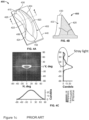
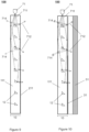
- Figs. 1a-1b shows a conventional lightguide 1 solution, wherein Fig. la is an opensurface lightguide and Fig. 1b is a lightguide comprising air-cavities 12A formed in a lightguide medium 2.
- Figs. 1a-1b shows a fundamental problem of undesired stray light in lightguides for frontlight-, backlight- and general illumination concepts, encountered by conventional solutions.
- Light leakage problem occurs in conventional surface relief patterns configured as open structures, as well as advanced cavity pattern structures. This is the common problem and there has been not reasonable solution offered yet.
- Fig. 1c illustrates a frontlight solution utilizing cavity optics known from U.S. Application publication no. 2018/0088270 (Tuohioja et al).
- Fig. 1c that depicts Figs. 4A-4C of the abovementioned publication provides, among others, a cross-sectional view of light distribution angles. Developing stray light is indicated by a circle on the conoscopic Fig. 4C (numbering pertains to that in the reference publication). Mentioned publication does not teach how to minimize the stray light problem; neither teaches how to optimize incoupled light distribution together with the first pattern surface design in order to achieve preferred illumination without stray light, which lowers viewing performance, e.g. contrast, of the display. The publication further lacks indication on dealing with decreased contrast performance and transparency caused by Fresnel reflection.
- known solutions generally involve extracting light by pattern profiles, wherein light arrives at said profiles at most suitable angles of incidence. Neither of these solutions deals with challenging angles of incident that involve development of stray light.
- An objective of the present invention is to at least alleviate each of the problems arising from the limitations and disadvantages of the related art.
- the objective is achieved by various embodiments of a transparent optical device, according to what is defined in the independent claim 1.
- the optical function or functions of the optically functional layer is/are established by an at least one of the: dimensions, shape, periodicity and disposition of the cavities within the feature pattern and by a fill factor value for said feature pattern.
- the exit surface is configured to transmit light with at least a refraction function.
- the entrance surface is configured to incouple light arriving thereto at a predetermined angle of incidence or a range of angles of incidence smaller than the critical angle relative to the surface normal, whereby outcoupled Fresnel reflection is avoided.
- the cavities in the at least one feature pattern 11 are configured to outcouple incident light arriving at the entrance surface, via a total internal reflection (TIR) function.
- TIR total internal reflection
- the cavities in the at least one feature pattern comprise an antireffective layer disposed at the entrance surface within an interior of the cavity. In an embodiment, the cavities in the at least one feature pattern further comprise an antireflective layer disposed at the exit surface within an interior of the cavity.
- the cavities are filled by a gaseous medium, preferably, with air.
- the embedded cavity features alternate with a plurality of related light passages.
- the embedded feature pattern is established in the light-transmitting carrier medium by a laminate structure formed by an entirely flat, planar layer of the carrier medium arranged against a patterned layer of the carrier medium, whereby a plurality of optically functional internal cavities is formed at an interface between the layers.
- the transparent optical device further comprises an antireflective layer disposed at the interface between the layers formed by the light-transmitting carrier medium.
- the embedded optical cavity features are selected from the group consisting of a groove, a recess, a dot, and a pixel, wherein said cavity features have crosswise profiles selected from: binary-, blazed-, slanted-, prism-, trapezoid-, hemispherical profiles, and the like, and wherein said features have lengthwise shape selected from: linear, curved, waved, sinusoid, and the like.
- the at least one feature pattern is a hybrid pattern comprising a plurality of discrete feature profiles and/or a plurality of at least partly continuous feature profiles.
- the at least one feature pattern is fully integrated and/or embedded within the light-transmitting carrier medium.
- the transparent optical device further comprises an at least one antireflective layer disposed on the optically functional layer , whereby the feature pattern is configured to cooperate, in terms of its optical function or functions, with said antireflective layer such as to avoid Fresnel reflection.
- the lightguide medium and the optically functional layer are an optical polymer and/or glass.
- the transparent optical device further comprises an at least one optical filter layer disposed on an at least one surface of the lightguide medium and provided with an at least one optical function through its entire surface coverage or at predetermined areas thereof, wherein the at least one optical function of said optical filter layer, in terms of at least the material it is formed of, is selected from: reflection, transmission, polarization, and refraction.
- said optical filter layer is formed of a substrate material having a refractive index lower than the refractive index of material constituting the optically functional layer and, preferably, lower than the refractive index of material constituting the lightguide medium.
- the optical filter layer is configured as a reflective Total Internal Reflection layer structure.
- the optical filter layer is disposed on both surfaces of the lightguide medium. In an embodiment, said optical filter layer is disposed between the lightguide medium and the optically functional layer.
- the optical filter layer comprises a plurality of optical apertures to enable light transmission therethrough, said apertures being arranged within a predetermined location at said optical filter layer or extending along and/or across an entire surface of said optical filter layer.
- the transparent optical device further comprises an optical contact layer configured to establish an optical bonding with at least a part of an illumination surface.
- said optical contact layer is a uniform layer optionally provided with an at least one feature pattern comprising a plurality of optically functional features.
- said optical contact layer is configured to establish a non-permanent optical joint with the illumination surface. In an embodiment, said optical contact layer is configured to establish a permanent connection with the illumination surface.
- the transparent optical device further comprises at least one light source.
- optical transparency is established in presence and in absence of illumination derived from said at least one light source.
- the transparent optical device is configured as a frontlight illumination device or a backlight illumination device.
- a non-claimed transparent illuminated article is provided, which article comprises the transparent optical device according to the embodiments.
- the solution provided hereby is advantageously realized as integrated (internal) cavity optics.
- light is often partially transmitted (penetrated) into said cavities, whereby undesired refraction and Fresnel reflection is caused and perfect light distribution control is not achievable.
- extracted light distribution in terms of reflection and refraction angles and directions, accordingly) can be finally controlled with high precision by TIR extraction functionality of the associated optically functional feature pattern.
- Optical transparency of the present device is attributable to a number of structural characteristics that allow for avoiding or at least minimizing an amount of scattered- and stray light caused by Fresnel reflections, for example.
- the solution allows for improving visual quality of an image on a display device, for example, by eliminating haziness, ghosting, formation of double images due to stray light, "washout" of colour display, and avoiding a lower display contrast.
- the solution can be utilized for frontlight and backlight, window and façade illumination, signage and signal lighting, solar applications, decorative illumination, light shields and masks, public and general illumination, such as roof lighting, and the like.
- frontlight and backlight window and façade illumination
- signage and signal lighting solar applications
- decorative illumination light shields and masks
- public and general illumination such as roof lighting, and the like.
- Present disclosure is focused on providing the optical device with markedly improved transparency with light off and on modes that further enables eliminating or at least minimizing harmful stray light and Fresnel reflections.
- the optical device presented hereby is primarily configured for light-coupling and illumination purposes. Transparency thereof is attained by thorough selection of materials and element design, which are targeted, on the whole, to minimizing stray light by a variety of ways, whereby Fresnel reflection is also minimized.
- optical and light are largely utilized as synonyms unless explicitly stated otherwise and refer to electromagnetic radiation within a certain portion of the electromagnetic spectrum, preferably, but not limited to, visible light.
- optical filter or a “light filter” refers, in the present disclosure, to a device or a material used to change the spectral intensity distribution or the state of polarization of electromagnetic radiation incident thereupon.
- the filter may be involved in performing a variety of optical functions, selected from: transmission, reflection, absorption, refraction, interference, diffraction, scattering and polarization.
- the term "lightguide” or “waveguide”) refers, in the present disclosure, to a device or a structure configured to transmit light therealong (e.g. from a light source to a light extraction surface).
- the definition involves any type of the lightguide, including, but not limited to a light pipe type component, a lightguide plate, a lightguide panel, and the like.
- carrier or “carrier medium” generally refers to a flat, planar member composed of a substrate material configured for light propagation and optionally constituting a layered structure.
- a number of refers herein to any positive integer starting from one (1), e.g. to one, two, or three; whereas the expression “a plurality of” refers herein to any positive integer starting from two (2), e.g. to two, three, or four.
- first and second are not intended to denote any order, quantity, or importance, but rather are used to merely distinguish one element from another.
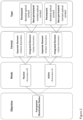
- FIG. 2 shows is a chart that defines different phases of feature characterization by which the transparent lightguide solution can be attained.
- the present disclosure thus provides inter alia for a lightguide solution whose transparency does not depend on illumination mode.
- the optical device 100, 100A is transparent when light is on and when light is off.
- Present solution further exploits a concept of light outcoupling (extraction) at predetermined angles, whereby undesired stray light can be avoided.
- the optical device 100, 100A can be configured to provide illumination for a single side of an illumination surface (such as a display or a poster) or dual-side illumination (such as a façade or a window). It is important to specify illumination purpose in each case, in view of preferred illumination distribution, visual angle range etc., in order to construct the optical device in a manner most beneficial for eliminating or at least minimizing undesired stray light, in particular, in display and facade illumination.
- an illumination surface such as a display or a poster
- dual-side illumination such as a façade or a window
- the present invention addresses a fundamental problem, in particular, in view of improving internal cavity performance by reducing stray light leakage at profile surfaces and eliminating or at least minimizing internal Fresnel reflection. Best results can be attained by combining two or more characteristic features. A number of primary solutions on achieving transparency and reduction of stray light / undesired Fresnel reflections are presented hereinbelow.
- Transparent lightguide and transparent cavity optics have many applications.
- the optical pattern itself has to be designed and optimized on a case-by-case basis.
- the at least one optical pattern provided within the optically functional layer is established by the relief forms selected from the group consisting of: a groove, a recess, a dot, and a pixel, wherein said relief forms have crosswise concave or convex profiles selected from: binary, blazed, slanted, prism, trapezoid, hemispherical, and the like, and wherein said relief forms have lengthwise shape selected from: linear, curved, waved, sinusoid, and the like.
- a transparent optical device referred to, in some instances, as a "transparent illumination device”, is illustrated at Fig. 11 .
- transparent we refer to a function of optical transparency generally defined as a physical property of material that allows photons arriving at a surface of said material to pass through the material unaffected, such as without being scattered, absorbed or back-reflected.
- Optical transparency of the present device 100 is established by a number of structural attributes described hereinbelow that allow for avoiding or at least minimizing an amount of scattered- and stray light caused by Fresnel reflections, for example, whereby visual haziness, ghosting and/or formation of double images due to stray light and colour “washout", etc. are further eliminated.
- 100A For different product configurations (e.g. frontlight, backlight, illumination plate for a variety of illuminated targets), it is important to understand fundamental criteria and requirements implied by the end product to proceed with.
- Present disclosure provides a comprehensive solution for transparent optical devices with internal cavity performance optimized, in particular, in terms of avoiding stray light produced by light leakage via the profile surfaces and/or by internal Fresnel reflection.
- Different configurations presented herein below involve a combination of two or more characteristics directed to attaining transparency and on avoiding stray light.
- the transparent optical device 100 hereafter, the optical device 100, comprises a lightguide medium 101 and at least one optically functional layer 10.
- the lightguide medium is advantageously configured for light propagation, whereas the optically functional layer 10 is configured to establish optical transparency of the device 101 via a control function over light incident thereto and via at least a light outcoupling function. Mentioned optical functions are attributable, in a non-limiting manner, to provision of at least one optically functional feature pattern 11 ( Fig. 9 ).
- Fig. 9 is a cross-sectional view of the optically functional layer 10.
- the layer 10 thus forms a light distribution structure and comprises at least one feature pattern 11 established in a light-transmitting carrier medium 111 by a plurality of embedded optical features.
- the optical features are formed by a plurality of internal optical cavities 12 (viz. internal, embedded or integrated cavity optics). The latter are further referred to as “cavities” or “cavity profiles”.
- FIG. 3l shows internal organization within the layer structure 10, whereupon an entirely flat, planar layer 111A of the carrier medium is arranged against a patterned layer 111B of the carrier medium such, that an internal (viz. embedded or integrated) feature pattern 11 is established at an interface between a patterned layer 111 and a planar layer 111A.
- the boundary between the carrier layers 111A, 111B is not shown to emphasize an essentially "one-piece" nature of the complete structure 10.
- the complete structure 10 is provided as a single layer.
- the optically functional layer 10 is provided in the form of a film, a sheet or a coating for a waveguide medium 101.
- the transparent optical device 100 thus comprises the lightguide medium 101 configured for light propagation, and the at least one optically functional layer 10 comprising at least one optically functional feature pattern 11 formed in a light-transmitting carrier medium 111 by a plurality of embedded features provided as optically functional internal cavities 12.
- Said at least one feature pattern 11 is further configured to perform an incident light control function and at least a light outcoupling function by establishing a predetermined incoupled light distribution at the pattern 11 and/or by modifying the refractive indices of materials and elements provided in the optical device and interfaces therebetween, whereby stray light is minimized and optical transparency of the device 100 is established.
- the optical function or functions of the optically functional layer 10 is/are established by an at least one of the: dimensions, shape, periodicity and disposition of the cavities 12 within the feature pattern 11 and by the Fill factor value for said feature pattern.
- Optical features such as cavities 12, are provided within a reference area, such as within the optically functional layer with the pattern 11.
- design parameters for said optical features such as fill factor and/or density, as well as period, pitch, height, length, angle, curvature, local pixel size, position, etc.
- Fill factor (FF) also referred to as filling factor, defined by a percent (%) ratio of the optical features 12 to a unit area, is one of the key parameters in designing optical solutions. FF thus defines a relative portion of the features 12 in the reference area.
- optically functional layer 10 with optical cavity pattern is typically design in an application-specific manner for transparent backlight, frontlight and illumination panels, whereby optical pattern design can be have or constant pattern density or gradient pattern density, wherein the Fill factor value for pattern density has to be at relatively low level, such as 10 - 50% of the total area.
- a range of Fill factor variation between the neighboring local regions should be approximately ( ⁇ ) 3%, whereas the same between the opposite corner regions - approximately ( ⁇ ) 20% in order to avoid / minimize pattern visibility due to high- and low Fill factor variations between different regions.
- Achieved transparency influences final efficiency; the more transparent is the solution, the greater efficiency can be attained. Maximal efficiency is attainable by both continuous periodic profiles and local profiles such as pixels.
- maximal Fill factor can be optimized in terms of transparency, haziness and stray light.
- One significant benefit is to have constant and efficient 3D optical pattern (solid filling factor design), which can be utilized for multiple applications. This reduces mastering and product costs, and makes possible producing optical devices of relatively large sizes, e.g. greater than 0,5 - 1,5 m 2 (square meters).
- a refractive index value (n1) of said carrier medium 111 exceeds the refractive index value (n2) of medium that fills the embedded cavities 12.
- the cavities 12 comprise at least a first surface 121, configured as an entrance surface to receive incident light and a second surface 122, configured as an exit surface, through which light exiting the cavity is transmitted in the medium 111 to be utilized for illuminating a target surface. Only light that follows a predetermined path, by being guided by the cavity pattern, disclosed hereby, can be exploited for illumination purposes.
- the light-transmitting carrier medium 111 is thus provided as an optical polymer or glass.
- the carrier medium 111 is polymethyl methacrylate (PMMA).
- the cavities 12 are filled with a gaseous medium. It is further preferred that the cavities 12 are filled with air. Nevertheless, any other gaseous medium, as well as any fluid, liquid, gel or solid, can be provided as a filling material for said cavities.
- Figs. 3a and 3i illustrate a configuration, in which light incident on the first (entrance) surface 121 is outcoupled (extracted) via a total internal reflection (TIR) or refraction.
- TIR total internal reflection
- this type of sole light management and arrangement requires a special light source with narrowed light distribution or light incoupling collimation in at least a vertical direction, whereby limiting a range of angles incident at the lightguide element.
- This solution requires e.g. approximately 10° vertical light collimation in order to achieve TIR function.
- Special optical arrangement is required for the light incoupling, which can be integrated into the light source or into the lightguide edge. Such arrangement may comprise an optical element and/or redirecting reflector layers on both surfaces of the lightguide in the incoupling area. Also, an absorption layer can be utilized, wherein all larger incident light angles are eliminated.
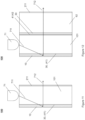
- Figs. 3b and 3j illustrate asymmetric cavity-optics solutions and a basic Fresnel reflection problem encountered thereby.
- Light is incident at the pattern (cavities 12) at such an angle / angles, at which light, when redirected inside the cavity 12, forms harmful stray light via Fresnel reflections.
- Fresnel-reflected (stray) light 714 can be further out-coupled from the pattern (dashed line) at a display surface.
- Fig. 3c shows a symmetric optical cavity solution, in which the first (entrance) surface 121 is configured to incouple incident light arriving thereat and to direct light rays into the cavity towards the second surface 122, and wherein the second surface 122 is configured to receive light rays arriving thereat and to transmit said light rays outside the cavity into the light-transmitting carrier medium 111 for propagation in said medium 11 and/or for outcoupling (out of the layer 10 / the device 100 toward an illumination surface).
- Fresnel reflection caused by the second surface 122 is not outcoupled from the cavity (trapped). Such pattern design minimizes undesired stray light.
- the second surface 122 configured to transmit and redirect light cooperates with the first surface 121 of a subsequent cavity 12, whereby light extraction/outcoupling efficiency can be improved by optimizing directions of light rays incident onto each (subsequent) cavity.
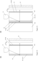
- Fig. 3d and 3k illustrate a configuration, for minimizing stray light by eliminating Fresnel reflection via provision of a layer 21 with additional optical functionality, such as an antireflective layer, on the first surface 121 ( Fig. 3d ) or on the second surface 122 ( Fig. 3k ), as discussed further below. Avoidance of Fresnel reflection is indicated by a crossed arrow.
- Fig. 3e illustrates a cavity-optics solution and a stray light problem encountered thereby.
- incident light is received at the first surface 121 and redirected inside the cavity 12, wherefrom light leakage occurs (stray light, Fig. 3e ), by refraction at a bottom surface of the cavity, i.e. at an interface between the cavity (n2) and surrounding medium (n1).
- undesired light strays and/or Fresnel reflection can be avoided or at least minimized by providing at least the first surface 121 to incouple light arriving thereto at a predetermined angle or a range of angles.
- the entrance surface 121 is configured to incouple and to further distribute light arriving thereto at a predetermined angle of incidence or a range of angles of incidence smaller than the critical angle relative to the surface normal, whereby outcoupled Fresnel reflection is avoided.
- Critical angle is an incident angle of light relative to the surface normal, at which a phenomenon of the total internal reflection occurs.
- the angle of incidence becomes a critical angle (i.e. equal to the critical angle), when the angle of refraction constitutes 90 degrees relative to the surface normal.
- TIR occurs, when light passes from a medium with high(er) refractive index (R i ) to a medium with low(er) R i , for example, from plastic (R i 1.4 - 1.6) or glass (R i 1.5) to the air (R i 1) or to any other media with essentially low refractive indices.
- Fig. 3f thus illustrates a solution enabling transmission of light through the optical pattern (the cavities 12), wherein light stray is avoided or at least minimized by limiting an angle of incidence ( ⁇ max ) at the first surface 121.
- ⁇ max an angle of incidence
- the first surface of the cavity profile is configured to limit a range of incident angles to values below the critical angle relative to the surface normal for avoidance of leaked stray light through the bottom interface.
- Angles of incidence can be limited by provision of an optical collimation element, a redirecting reflector or an absorption layer (not shown) at the surface 121 (light incoupling edge), wherein vertical light distribution is required to be in the range of approximately ( ⁇ ) 15°.
- the first surface 121 of the cavity can be constructed / designed to enable proper (further) outcoupling and transmission of light through the optical pattern, whereby stray light is minimized by limited angle of incident ( ⁇ max ).
- ⁇ max a cos n 3 n 1 wherein n3 is the refractive index (R i ) of an external medium outside the lightguide (viz. outside the light-transmitting carrier 111; see Fig. 17, A ).
- the first surface 121 has to be modified in order to incouple incident light and to redirect thus incoupled light to a predetermined, single focus point at the opposite wall 122, preferably close to the bottom surface (interface), whereby stray light can be avoided.
- the entrance surface 121 is further configured to incouple light arriving thereto with a collimation function and to direct light rays into the cavity such that light propagates through the cavity while avoiding hitting any other surface except the exit surface 122.
- Fig. 3g further illustrates a solution enabling transmission of light through the optical pattern (the cavities 12), by modifying an at least first surface profile (shown by a dashed triangle further enlarged at Fig. 3h ).
- the solution allows for avoiding or at least minimizing light stray by modifying a refraction angle of incident light (dashed line).
- n3 is the refractive index (Ri) of an external medium outside the lightguide (viz. outside the light-transmitting carrier 111)
- ⁇ is the variable angle as a function of the surface profile.
- the first surface 121 is configured such as to incouple and to (pre)collimate light arriving thereto, whereby incoupled, (pre)collimated light distribution is established inside the cavity, in which light is further directed towards the second (exit) surface (the bottom surface is not hit).
- Figs. 3f, 3g illustrate a solution, in which light propagating in the cavity 12 does not hit the bottom surface of said cavity, whereby the stray light problem ( Fig. 3e ) is avoided.
- the layer structure 10 further comprises an antireflective layer 21 disposed at the interface between the sublayers 111A, 111B formed by the light-transmitting carrier medium 111.
- an antireflective layer 21 disposed at the interface between the sublayers 111A, 111B formed by the light-transmitting carrier medium 111.
- a plurality of embedded (internal) cavity features 12 thus alternate with a plurality of related light passages 13.
- Said light passages 13 are light-transmitting carrier medium material 111.
- the cavities can be provided with the antireflective layer 21 at the first-(entrance) and/or the second- (exit) surfaces thereof.
- the antireflective layer 21 can be configured as a coating or a structure, preferably, as a broadband anti-reflection (AR) by an AR pattern or a multi-layer coating or a low refractive index (R i )-coating, in order to minimize e.g. Fresnel reflection ( Fig. 3d , 3k ).
- AR broadband anti-reflection
- R i low refractive index
- the optically functional layer 10 can be further configured to comprise the optical cavities 12 established with the three-dimensional profiles selected from one of the essentially blazed, curved or wave-shaped profiles. In some instances it is preferred that the optical cavities 12 are established with the three-dimensional profiles provided as symmetrical sinusoidal waveforms or asymmetrical sinusoidal waveforms.
- the at least one optical feature pattern 11 can be established by the optical features selected from the group consisting of: a groove, a recess, a dot, and a pixel, wherein said features have crosswise concave or convex profiles selected from: binary, blazed, slanted, prism, trapezoid, hemispherical, microlens and the like, and wherein said structures have lengthwise shape selected from: linear, curved, waved, sinusoid, and the like.
- Said at least one optical feature pattern 11 can be configured as: a periodical grating structure, micro- and nano-optical profiles, discrete patterns, grating pixel pattern (local periodic), and the like.
- the smallest pattern features (cavities) 12 can be further optimized and minimized.
- the sharp tips can be optimized and minimized by cutting off, rounding or flattening, in order to minimize particular scattering.
- Such an arrangement solves a problem common for conventional solutions, wherein the optical pattern profiles may cause scattering of diffraction distortion, known as a rainbow effect, which is some cause undesired performance.
- Exemplary pattern solutions for transparent illumination are further presented on Figs. 15 and 16 .
- the optical cavity pattern solution can be provided with comprising relatively small pattern features (not exceeding 25 ⁇ m), which cannot be captured by human eye. Whether larger features are utilized, it is preferred that AR-coatings or AR-patterns are further provided on the profile surfaces (hybrid pattern; Figs. 3d , 3k, 3l ), which makes the pattern less visible to human eye. It is preferred that cavity surface quality is of optical grade, whereby scattering can be effectively avoided, and so stray light.
- Fig. 15 thus shows the exemplary pattern features 12 for transparent illumination, in particular, for "invisible" (to human eye) pattern size.
- Pattern properties are provided in the table 1 hereinbelow. Table 1 .
- Pattern properties for exemplary profiles A and B (Fig. 15).
- Property Exemplary profile A Exemplary profile B Pattern height 5 ⁇ m 2.5 ⁇ m Pattern length 43 ⁇ m 21.5 ⁇ m Front face angle 54° 54° Back face angle 85° 85° Tip radius 0.5 ⁇ m 0.5 ⁇ m In/out feed angle 26° 26°
- the profiles can be fabricated by fast tool servo (FTS) machining, for example.
- FTS fast tool servo
- profile parameters are adjustable to achieve desired performance. Additionally adjustable parameters include profile orientation, provision of a single pattern or a periodic pattern, provisions of discrete (pixel) pattern or continuous pattern, etc.
- the optical feature pattern 11 comprising the above described cavity profiles can be generally referred to as a "hybrid" pattern that comprises a plurality of discrete feature profiles and/or a plurality of at least partly continuous feature profiles.
- Said hybrid pattern can thus be configured as a discrete pattern (e.g. a pixel) or as a continuous pattern.
- said hybrid pattern can be configured to comprise a plurality of optical features 12 provided as discrete profiles or at least partly continuous profiles.
- the optically functional layer 10 can be further configured such, that within the at least one optical feature pattern, the plurality of optical cavities 12 is arranged into an array or arrays extending along and/or across an entire area occupied by said feature pattern (not shown).
- the transparent optical device 100 further comprises an at least one optical filter layer 41, 42 (a light filter layer) disposed on at least one surface of the lightguide medium 101 and provided with at least one optical function through its entire surface coverage or at predetermined areas thereof. Mentioned optical function is selected from at least: reflection, transmission, polarization, and refraction.
- the optical filter layer 41, 42 is disposed on both surfaces of the lightguide medium 101.
- the light filter layer 41, 42 is preferably configured as a thin film with a layer (film) thickness (h > ⁇ ) within a range of 0,2 - 50 micrometers ( ⁇ m).
- layer thickness can vary within a range of 0,2 - 50 micrometers ( ⁇ m), preferably, within a range of 0,2 - 10 ⁇ m.
- the light filter layer 41, 42 is composed of the substrate material provided as a so called low refractive index material and having the refractive index within a range of 1,10 - 1,41. In any event the refractive index of the light filter layer is provided below 1,5; preferably, below 1,4.
- the light filter layer contains nano-silica material in a mesopo-rous film.
- the low R i cladding interphase is coated, laminated or bonded with a low-(out)gassing material in order to sustain an index value.
- the light filter layer 41, 42 is configured as a total internal reflection layer structure.
- the filter layer 141 can thus be implemented as a reflective TIR solution, based on available TIR materials, such as TiO 2 , BaSO 4 , SiO 2 , Al 2 O 2 , Al, Ag, dielectric materials and high reflection (HR)-coating materials.
- the light filter layer 41, 42 is formed of a substrate material (second medium, n2, Fig. 4a ) having the refractive index (R i ) lower than the refractive index of the material constituting the optically functional layer 10, 111 and/or the optically transparent (lightguide) substrate 101 (first medium, n1, Fig. 4a ), whereby n1 > n2 ( Fig. 4a ).
- Relationship between the refractive index (R i ) value of the light filter layer and the lightguide-related parameters, such as an average brightness (Nits) and extraction efficiency (%) is shown in Table 2 below.
- the expression "low R i layer” refers to the light filter layer 41, 42. Table 2 .
- the optical filter layer is a cladding, a coating or a film.
- the optical filter layer can be configured as a continuous, uniform layer 42.
- the optical filter layer (41) can comprise a plurality of optical apertures 41A to enable light transmission therethrough, said apertures being arranged within a predetermined location at said optical filter layer or extending along and/or across an entire surface of said optical filter layer ( Figs. 4a-4c ).
- the optical apertures 41A are configured adjustable in terms of their dimensions, size and/or shape thereof.
- the apertures can be essentially circular or rectangular, with the size in either format provided in a range of 0,5 - 50 ⁇ m, preferably, within a range of 1 - 30 ⁇ m.
- the aforesaid range is indicative of any one of the length and/or width parameters.
- the aforesaid range is indicative of an individual aperture diameter.
- the depth parameter is defined by the thickness of the light filter layer 41 and it is provided within the range of 0,2 - 50 ⁇ m, as defined hereinabove.
- the apertures 41A can be provided as continuous structures, extending over larger areas (in comparison to mentioned above), and having any arbitrary shape.
- Aperture density and/or the fill factor (per a surface area unit) can be constant (within a range of 0,1% - 100%).
- the apertures are established in the light filter layer 41 in a predetermined manner.
- provision of apertures is uniform (with constant size, shape and periodicity) along an entire length of a light distribution element, such as a lightguide, i.e. from a light source (e.g. LED) end to the opposite end.
- the apertures can be provided variable in terms of at least size, shape or periodicity from the LED end to the opposite end.
- the apertures can be arranged with a variable density utilizing gradual fill factor.
- the light distribution element can be configured to include the light filter layer 141 with the apertures, whose size gradually increases from said LED end to the opposite side.
- the optically functional layer with the pattern 11 is primarily configured to propagate and (out)couple light incident thereto
- the light filter layer is configured to selectively control and filter light incident thereto and/or propagating via the lightguide.
- the apertures 41A can be further configured, individually or collectively, to perform a variety of functions, such as light transmission, scattering, refraction, reflection, and the like.
- the aperture(s) can be configured to provide the light outcoupling function.
- the optical filter can further include apertures with varying optical functionalities, including, but not limited to optical refractive index, non-reflective material, higher optical density, different optical contrast, etc., which provide for light transmitting therethrough and form as a light channel, and have light- and wave- controlling and/or filtering properties to achieve a predetermined light-/signal figure, distribution and efficiency for illumination purposes.
- optical functionalities including, but not limited to optical refractive index, non-reflective material, higher optical density, different optical contrast, etc.
- the apertures in the light filter layer can be further filled with a fill material having the refractive index same or higher, as compared to the refractive index of the material the optically transparent (lightguide) substrate 101 is made from.
- Figs. 4a and 4b shows an optical device, embodied at 100A, as an optical pattern-free lightguide element.
- the transparent optical device 100A thus comprises the lightguide medium 101 configured for light propagation, the optical filter layer 41, 42 disposed on an at least one surface of the lightguide medium and provided with an at least one optical function established through its entire surface coverage or at predetermined areas thereof by at least the material said optical filter layer is made of.
- Said optical filter layer is a continuous layer formed of a material having a refractive index lower than the refractive index of the material constituting the lightguide medium.
- the optical filter layer 41, 42 is configured to minimize scattering of light rays propagating through the transparent optical device by the at least one optical function selected from: reflection, transmission, polarization, and refraction.
- Fig. 4a thus illustrates a lightguide concept without optical pattern(s) 11.
- the frontlight solution shown on Fig. 4a comprises the lightguide medium 101 laminated between optical filter layers 41, 42.
- Fig. 4a shows an example, wherein the lower optical filter layer 41 comprises optical apertures 41A, whereas the upper optical filter layer 42 is configured as the uniform layer without apertures.
- the lightguide 101 can be made of plastic (PMMA, PC) or glass.
- the stack is disposed on an illumination surface 51 (a paper like display or a printed poster, for example), and can be further covered with a cover 62 (hereby, a top cover made of plastic or glass, for example), with an adhesive layer 30, such as optically clear adhesive (OCA), for example.
- OCA optically clear adhesive
- the enlarged boxes (Option 1, Option 2) light propagates through the apertures 41A, from the lightguide medium 101 (n1, first medium) to an underlying layer 30 (n1, second medium), which has about the same refractive index than the first medium (however, higher or lower R i values may not be excluded).
- the refractive index of apertures formed at an interface between the lightguide 101 and, hereby, an underlying layer 30 ( Fig. 4a ) or an overlaying layer (not shown) typically matches with R i values of the first- and/or the second medium n1, whereas the R i value of the optical filter (n2) comprising said apertures, is generally lower than n1.
- the light filter layer 41, 42 can be configured as a transparent, low refractive index filter layer or as reflective TIR layer (e.g. diffusive or specular TIR layer) formed on the at least one side of the optically transparent (lightguide) substrate 101 or at or both sides thereof (top and bottom surfaces).
- Said optical filter can be: a) applied directly on a flat surface, b) laminated by an adhesive layer, or c) bonded by chemical surface treatment such as VUV (vacuum UV), atmospheric plasma treatment or microwave assisted bonding.
- the light filter layer 41, 42 has gradually variable low R i values to provide preferred light distribution even in an absence of apertures.
- the apertures 41A within the light filter layer 41 can be optically modulated, whereby a variety of light distribution patterns produced by the light filter layer can be attained, including, but not limited to: uniform, symmetric, discrete, or asymmetric light distribution patterns.
- the optical filter layer 41 including optical apertures 41A is thus provided on an at least one side of the lightguide medium.
- the optical filter can thus include apertures with varying optical functionalities, including, but not limited to optical refractive index, non-reflective material, higher optical density, different optical contrast, etc., which provide light passing through it such as a light channel and have light- and wave- controlling and/or filtering properties to achieve a predetermined light-/signal figure, distribution and efficiency for illumination purpose.
- Light distribution by the optical apertures forming a predetermined figure / image or signal can be uniform, non-uniform or discrete. Thereby, uniform, non-uniform or discrete image / figure or signal can be formed.
- Apertures can be provided on both sides of the optical filter layer forming uniform / continuous or discrete areas.
- the apertures can be provided throughout the entire surface of the optical filter layer or at predetermined areas thereof.
- the principal function of apertures is to control the amount of incident light propagating from the first medium to the second medium without light out-coupling, meaning all incident light angle is larger or the same as the critical angle in the medium. Especially, light uniformity control can thus be achieved without optical pattern.
- Optical apertures have a number of primary functions, such as transmitting light therethrough from the first medium to the second medium, which determines desired light distribution and/or uniformity.
- Light distribution in the first and second medium typically has an incident light angle below the critical angle (an angle of incidence above which TIR occurs) with regard to the medium interface, when air or low Ri filter / -cladding are forming the interface. As a result, light is not out-coupled from the medium.
- Fig. 4b shows the optical device 100A configured as a frontlight solution, in which the lightguide 101 is arranged on the top of the stack (i.e. it is not laminated between layers).
- Configuration comprises a single optical filter layer 41 configured as a low R i cladding with apertures.
- a topmost surface of the lightguide can be further deposited with a hard coating with preferably low R i value in order to prevent light leakage upon top surface contamination or defect.
- Fig. 4c illustrates the optical device 100 solution for frontlight illumination that comprises the optically functional layer 10 configured as the cavity optics lightguide, and uniform optical filter layers (low R i cladding layers) 42 provided on both sides of the light-transmitting carrier medium 111. Mentioned optical filter layers 42 can be applied onto the medium 111 surface directly or indirectly (viz. by means of adhesive or without adhesive).
- Fig. 4c thus comprises the light filter without apertures and with an optical pattern, such as an outcoupling pattern.
- the optical pattern 11 is fully integrated inside the lightguide medium 111 and may have different forms or shapes, such as micro-lens, blazed- or slanted forms, discrete pattern or multiple pattern pixel forms, which has periodical and grating features.
- Lightguide element is laminated, bonded with an adhesive 30, such as optically clear adhesive (OCA) or liquid optically clear adhesive (LOCA), and the like, which has higher R i than the low R i cladding 42, preferably the same refractive index than the lightguide medium 111 has.
- Fig. 4c thus shows a stack solution, in which the optically functional layer 10 provided with the optical filter layers 42 at both sides thereof is further laminated between the display surface 51 (hereby, a reflective display or a poster) and the top cover layer 62 made of plastics or glass.
- the optically functional layer 10 comprises cavity features 12 having non-identical shapes.
- the same configuration having identical shapes can be further provided.
- incident light is coupled by means of the optical cavity pattern(s) 11 into a first medium 111 to achieve a smaller incidence angle than the critical angle (relative to the surface normal), in order to transmit light through the low R i cladding 42 towards a second medium.
- the second medium may comprise an optical pattern solution (not shown) configured for light out-coupling to form preferred light distribution and illumination.
- the second medium may be void of the optical pattern configured specifically for light directing; thereby, the optical pattern shall outcouple light with preferred angle distribution.
- Provision of the optical device comprising the optical filter layer 42 (without apertures) as a lower layer, further topped with the optically functionally layer 10, has benefits that such structure can couple and direct light reflected from the bottom reflector back to the first medium 111, whereby a preferred light distribution is established.
- the optical device shown on Fig. 4c thus comprises the lightguide medium 111 for incoupled light propagation together with optical filters 42 for light distribution uniformity control.
- the cavity pattern is configured such that angle at which light is incident on the pattern is equal to or exceeding the critical angle ( ⁇ ⁇ C ) in the medium.
- Optical pattern 11 is preferably a uniform pattern with a constant Fill factor, with full filling or with discrete filling. Variable Fill factor may support preferred illumination- or signal indication objective.
- Fig. 9 being illustrative of a fundamental solution aiming at minimizing stray light by Fresnel reflection via provision of an antireflective layer 211 on a light extraction surface (extracted light 712) of the optical device 100, which is not in optical contact with an illumination surface.
- the AR layer is formed by a single layer or a multilayer coating or by an AR nanostructured layer.
- top surface is a light extraction surface for single-side ambient illumination
- said top surface can be provided with the AR-layer 211 (AR-coating or AR-pattern) on its outer side in order to minimize undesired Fresnel reflection in the opposite direction.
- the transparent optical device 100 further comprises the at least one antireflective layer 211 disposed on the optically functional layer 10, whereby the feature pattern 11 is configured to cooperate, in terms of its optical function or functions, with said antireflective layer 211 such as to avoid Fresnel reflection.
- the antireflective layer 211 can comprise a polarizer.
- Fig. 10 illustrates a fundamental solution aiming at minimizing stray light by Fresnel reflection via provision of an optical contact layer 31 configured to establish an optical bonding with at least a part of the illumination surface 51, such as a display surface.
- the optical contact layer is configured to establish the optical contact with the illumination surface or at least a part of by e.g. traditional optical contacting, wherein the surfaces are bonded together without any adhesives or mechanical attachments.
- the optical contact layer 31 can be provided for the entire surface 51 or for part of said surface. In some configurations the optical contact layer 31 is provided as a uniform layer. In some other configurations, the optical contact layer 31 can be further provided with an at least one feature pattern comprising a plurality of optically functional features (e.g. optical patterns, extraction features, etc.). In an event said pattern is not in the contact, it should be applied as close as possible to the illuminated surface 51. It is preferred that said pattern in the optical contact is configured, in terms of dimensions, as small as to remain invisible to human eye.
- the optical device can further comprise an additional AR layer at every interface, such as between the lightguide 111 and the optical bonding 31 (not shown). This can further minimize Fresnel reflection
- Fig. 10 thus shows a solution for minimizing Fresnel reflection stray light by optical bonding on the light extraction surface of the lightguide element.
- Optical bonding forms optical contact with illumination surface, such as display, and it can be utilized in full- or partial area of the illumination surface.
- Optical contact can be formed by optical patterns, extraction features, as well. Additional AR layer, AR coating or AR-pattern in every interface, e.g. between lightguide and bonding, can minimize the Fresnel reflection.
- the optical contact layer 31 is configured to establish a non-permanent optical joint with the illumination surface 51.
- the optical contact layer 31 is configured to establish permanent connection with the illumination surface 51.
- Fig. 11 illustrates the transparent optical device 100 configured as a transparent illumination element for ambient lighting.
- the device 100 shown on Fig. 11 device comprises the lightguide medium 101, an optical extraction layer 10 laminated at one side of the lightguide medium 101 and the antireflective layer 211 on the outer side.
- the optically functional layer 10 comprises an at least one extraction pattern with constant density or gradual density.
- the layer 10 can be laminated to the lightguide medium 101 by an adhesive layer 30, optionally comprising an optical filter layer (low R i layer), preferably configured as the optical filter layer 41 with apertures.
- an optical filter layer low R i layer
- Fig. 12 illustrates the transparent optical device 100 configured as a transparent illumination element for ambient lighting.
- the device 100 shown on Fig. 12 comprises the lightguide medium 101, the optical extraction layer 10 laminated to one side of said medium 101 and the cover 62 at the other side of said medium 101.
- the cover is further provided with the AR layer 211 at an external side (light extraction surface).
- the lightguide medium can be laminated to the cover 62 by the adhesive layer 30 optimally provided with the optical filter layer 41, 42 (with or without apertures).
- Fig. 13 illustrates the transparent optical device 100 for display lighting.
- the stack includes a lightguide medium 101 with the optically functional layer 10 for optical extraction at one side of the lightguide 101 and the optical filter layer with or without apertures 41, 42 at another side of the lightguide.
- the stack can include the optical filter layer configured as the low R i cladding, preferably, the cladding with apertures (layer 41), also between the optically functional layer 10 and the lightguide medium 101, in conjunction with the adhesive layer 30, configured as optically clear adhesive (OCA), for example.
- OCA optically clear adhesive
- the stack can further comprise the optical contact layer 31 at the illumination side, provided in conjunction with the low R i cladding layer 41/42.
- Said optical contact layer 31 is preferably configured as a non-permanent bonding layer formed by elastic, essentially soft optical material.
- Fig. 14 illustrates the transparent optical device 100 for display lighting. Configuration generally follows the solution shown on Fig. 13 ; however, the stack shown on Fig. 14 additionally includes the cover 62, such as a cover glass, laminated with the optically functional layer 10. The solution further comprises the optical filter layer 41, 42 (with or without apertures) provided between the optically functional layer 10 and the cover glass 62. Similarly to Fig. 13 , the stack includes the optical contact layer 31 configured as the non-permanent bonding layer formed by elastic, essentially soft optical material.
- the optical contact 31 between the lightguide 111, 101 and the illumination surface 51 can be further provided as a rigid optical material.
- the optical boding 31 contacts the illuminated surface 51, in order to minimize stray light and keep the contrast ratio high. It is preferred that the layer 31 is manufactured form durable material, to attain reliability upon several openings (for non-permanent solutions).
- the transparent optical device 100 comprises the optical filter layer 41, 42 disposed between the lightguide medium 101 and the optically functional layer 10.
- a transparent optical device 100 comprising a lightguide medium 101 configured for light propagation, an at least one optically functional layer 10 comprising at least one optically functional feature pattern 11 formed in a light-transmitting carrier medium 111 by a plurality of embedded features provided as optically functional internal cavities 12, which at least one feature pattern 11 is configured to perform at least a light outcoupling function, and an optical contact layer 31 configured to establish a non-permanent, re-openable optical joint with an illumination surface 51.
- the device 100, 100A further comprises an at least one light source 71, selected from: a Light Emitting Diode (LED), an Organic Light Emitting Diode (OLED), a laser diode, a LED bar, an OLED strip, a microchip LED strip, and a cold cathode tube.
- LED Light Emitting Diode
- OLED Organic Light Emitting Diode
- laser diode a laser diode
- LED bar a LED bar
- OLED strip an OLED strip
- microchip LED strip a microchip LED strip
- cold cathode tube a cold cathode tube
- Optical transparency of said optical device is established in presence and in absence of illumination derived from said at least one light source 71.
- the transparent optical device is configured as a frontlight illumination device or a backlight illumination device. Hybrid illumination with transparent frontlight and backlight can thus be attained, which can be switched for different modes, viz. a transparent mode with transparent directional lightguide on top of the illuminated surface 51 / display (illumination away) and a non-transparent mode with light mask with transparent lightguide on the backside of display (illumination towards).
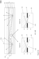
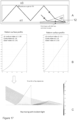
- Fig. 5 being illustrative of a fact that pattern profiles and angular control of incident light have an influence on light extraction efficiency and stray light development.
- Figure 5 thus illustrates stray light minimization by a hybrid solution, wherein the first surface 121 of the pattern cavity profile 12 combines light received at limited angles of incidence, smaller than the critical angle relative to the surface normal, whereby light leakage, such as stray light is effectively avoided.
- Diagrams on the upper side of Fig. 5 can be illustrative of the solution shown on Fig. 3e , whereas the same on the lower side can be illustrative of the solution shown on Fig. 3f .
- Optical cavities 12, in particular, in terms of first surfaces 121 thereof can be designed such as to enable controlling an angle or a range of angle of incident light arriving at said surface.
- Fig. 5 one may observe that by narrowing the incident light angle one can markedly reduce change stray light from the flat bottom surface. Compare upper figure showing light incident at an angle 26.5° (strong stray light) with the lower figure showing light incident at an angle 19.4 ° (minimized stray light) showing a remarkable improvement in terms of minimizing stray light. This is very important design criteria for producing improvements in terms of light extraction and reduction of stray light.
- the same improvement can be achieved by cavity profile optimization by equation, especially advanced equation for optimizing the bottom side/or and shape of the cavity profile ( Fig. 3g, 3h ).
- the first surface of said cavity profile can be defined by equations 2, 3 presented hereinabove.
- Limitation of incident light angle ranges in the lightguide can be achieved and controlled by at least partially collimating incoupled light (at the first surface 121) or by absorbing light arriving at larger angles (compared to the critical angle) of incident light in the incoupling region. The latter is attained by provision of the antireflective layer 21 at the surface 121 ( Fig. 3d ).
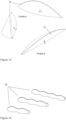
- Fig. 6 is illustrative of the fact that design of pattern cavity profiles has an influence on light extraction efficiency and stray light development.
- Fig. 6 demonstrates relationship between the cavity contact angle (realized as a micro-lens solution), light extraction efficiency and stray light development as follows: providing the indication of contact angle impact on the light intensity and extraction distribution; illustrating the results of basic simulation for different ML contact angles; and providing charts for light extraction and intensity distribution (without spatial dependency).
- the optical cavity profile 12 and, in particular, its first (entrance) surface has to be designed bearing in mind optimized light extraction and stray light ratio.
- Air-cavity microlenses ( Figs. 3i-3l ) are beneficial in terms of developing less stray light, possessing higher extraction efficiency and better (extracted light) distribution, in comparison to conventional micro-lens solutions.
- the contact angle for the ML profile is simulated in terms of extraction angle value, extraction efficiency and stray light level.
- Fig. 7 compares the optical device 100 (micro-lens air-cavity design) and a conventional frontlight, in terms of micro-lens light extraction and reduction of stray light.
- the optical device 100 is configures as a stack comprising the air-cavity lightguide configured as the optically functional layer 10 with the cavities 12 laminated (top or bottom) to a light absorbing surface 61 by the adhesive 30, preferably, optically clear adhesive (OSA), further comprising the optical filter 41 or 42 (low R i cladding with or without apertures).
- OSA optically clear adhesive
- a conventional micro-lens frontlight solution is thus compared with the air-cavity micro-lens frontlight solution by analysing both light extraction efficiency with its angular distribution and stray light ratio, wherein bottom and top surfaces have been applied an absorbing layer for each analysis.
- the solution 100 configured as the air-cavity micro-lens frontlight has over 2.5 times higher light extraction, better distribution angle, over 14 times better stray light ratio compared to the conventional solution.
- Fig. 7 is an example demonstrating an impact of the pattern profile on final result.
- One of the main goals here is avoidance of light penetration inside the pattern profile via critical incident angle, which may cause more stray light by reflection.
- Fig. 8 illustrates that the antireflective (AR) layer 21, 211 has an influence on development of stray light.
- A stray light by Fresnel reflection is shown.
- B improved stray light by minimized Fresnel reflection is shown.
- Improvements in view of minimizing Fresnel stray light, can be provided by pattern design, as well as and internal (21) and external (211) AR-layer arrangements, like at interior surfaces of the cavities (21) or at the bonding interface (211).
- achievable stray light value can be over 20 times lower than the original.
- optical pattern cavity profiles 12, and their first extraction surface and the second transmitting surface can be designed in combination with the internal AR-layer 21 to achieve improved light extraction and stray light level ( Fig. 3d , 3k, 3l ).
- the AR-layer 21 can be formed by a single layer coating or by multilayer coatings. Also the AR nanostructure can be utilized, in particular, in cavity optics, wherein one slanted surface can provide reasonable demoulding and replication. AR-layer thus works for two directions in the surface. Pattern profile then has hybrid structure, whereby light refraction and anti-reflection can be executed ( Figs. 3d , 3k, 3l ).
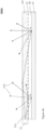
- Fig. 17 further illustrates a design method for pattern surface profiles 12, in particular, for the bottom areas thereof, in terms of light redirecting such as to minimize stray light, light leakage from said bottom surface(s). Calculation(s) are performed according to the advanced equation (3) (shown also on Fig. 3h ). Ray tracing model ( Fig. 17, C ) further depicts light transmission through the opposite surface.
- a transparent illuminated article that comprises the transparent optical device 100, 100A as described herein above.
- Said transparent illuminated article can be configured as a window, a façade illumination and/or indication element, a roof illumination and/or indication element, a signage, a signboard, a poster, a marketing board, an advertisement board illumination and/or indication element, and an illumination element configured for solar applications.
- optical device 100, 100A Use of the optical device 100, 100A is provided in illumination and indication solutions.
- use of the device 100, 100A is provided in decorative illumination, in illumination of light shields and masks, in public and general illumination, including window-, façade- and roof illumination-, signage-, signboard-, poster-, marketing board- and/or an advertisement board illumination and indication, and in solar applications.
Landscapes
- Physics & Mathematics (AREA)
- General Physics & Mathematics (AREA)
- Optics & Photonics (AREA)
- Engineering & Computer Science (AREA)
- Manufacturing & Machinery (AREA)
- Planar Illumination Modules (AREA)
- Optical Elements Other Than Lenses (AREA)
- Light Guides In General And Applications Therefor (AREA)
- Theoretical Computer Science (AREA)
- Laminated Bodies (AREA)
- Illuminated Signs And Luminous Advertising (AREA)
- Glass Compositions (AREA)
- Optical Communication System (AREA)
Claims (13)
- Transparente optische Vorrichtung (100), umfassend:ein Lichtleitermedium (101), das für die Ausbreitung von Licht konfiguriert ist, undmindestens eine optisch funktionelle Schicht (10), die mindestens ein optisch funktionelles Merkmalsmuster (11) umfasst, das in einem lichtdurchlässigen Trägermedium (111) durch eine Vielzahl von eingebetteten Merkmalen gebildet wird, die als optisch funktionelle Innenhohlräume (12) bereitgestellt sind,wobei das mindestens eine Merkmalsmuster (11) so konfiguriert ist, dass es eine Steuerfunktion für einfallendes Licht und mindestens eine Lichtauskopplungsfunktion ausführt, indem es eine vorbestimmte eingekoppelte Lichtverteilung an dem mindestens einen Muster (11) herstellt und/oder die Brechungsindizes von Materialien und Elementen, die in der optischen Vorrichtung bereitgestellt sind, und von Grenzflächen dazwischen modifiziert, wodurch
Streulicht minimiert wird und die optische Transparenz der Vorrichtung (100) hergestellt wird;wobei die Hohlräume (12) in dem mindestens einen Merkmalsmuster (11) eine Eintrittsfläche (121) und eine Austrittsfläche (122) umfassen, wobei die Eintrittsfläche (121) so konfiguriert ist, dass sie einfallendes Licht, das dort ankommt, einkoppelt und Lichtstrahlen in den Hohlraum in Richtung der Austrittsfläche (122) lenkt, und wobei die Austrittsfläche (122) so konfiguriert ist, dass sie Lichtstrahlen, die dort ankommen, empfängt und die Lichtstrahlen außerhalb des Hohl-raums in das lichtdurchlässige Trägermedium (111) zur Ausbreitung und/oder zur Auskopplung überträgt;dadurch gekennzeichnet, dass die Eintrittsfläche (121) weiter so konfiguriert ist, dass sie dort ankommendes Licht mit einer Kollimationsfunktion einkoppelt und Lichtstrahlen in den Hohlraum lenkt, so dass sich Licht durch den Hohlraum ausbreitet, während es vermieden wird, auf irgendeine andere Fläche außer der Austrittsfläche (122) zu treffen. - Transparente optische Vorrichtung (100) nach Anspruch 1, wobei die optische Funktion oder Funktionen der optisch funktionellen Schicht (10) hergestellt ist/sind durch mindestens eines von: Abmessungen, Form, Periodizität und Anordnung der Hohlräume (12) innerhalb des Merkmalsmusters (11) und durch einen Füllfaktorwert für das Merkmalsmuster.
- Transparente optische Vorrichtung (100) nach einem vorstehenden Anspruch, wobei die Austrittsfläche (122) so konfiguriert ist, dass sie Licht mit mindestens einer Brechungsfunktion überträgt.
- Transparente optische Vorrichtung (100) nach einem vorstehenden Anspruch, wobei die Eintrittsfläche (121) so konfiguriert ist, dass sie Licht, das unter einem vorbestimmten Einfallswinkel oder einem Bereich von Einfallswinkeln, der kleiner als der kritische Winkel relativ zu der Oberflächennormalen ist, dort ankommt, einkoppelt, wodurch eine ausgekoppelte Fresnel-Reflexion vermieden wird.
- Transparente optische Vorrichtung (100) nach einem der Ansprüche 1 oder 2, wobei die Hohlräume (12) in dem mindestens einen Merkmalsmuster (11) so konfiguriert sind, dass sie einfallendes Licht, das an der Eintrittsfläche (121) ankommt, über eine Funktion der internen Totalreflexion (TIR) auskoppeln.
- Transparente optische Vorrichtung (100) nach einem vorstehenden Anspruch, wobei die Hohlräume (12) in dem mindestens einen Merkmalsmuster (11) eine Antireflexionsschicht (21) umfassen, die an der Eintrittsfläche (121) innerhalb eines Innenraums des Hohlraums angeordnet ist.
- Transparente optische Vorrichtung (100) nach einem vorstehenden Anspruch, wobei die Hohlräume (12) in dem mindestens einen Merkmalsmuster (11) weiter eine Antireflexionsschicht (21) umfassen, die an der Austrittsfläche (122) innerhalb eines Innenraums des Hohlraums angeordnet ist.
- Transparente optische Vorrichtung (100) nach einem vorstehenden Anspruch, wobei sich in dem Merkmalsmuster (11) die eingebetteten Hohlraummerkmale (12) mit einer Vielzahl von zugehörigen Lichtdurchgängen (13) abwechseln.
- Transparente optische Vorrichtung (100) nach einem vorstehenden Anspruch, wobei das eingebettete Merkmalsmuster (11) in dem lichtdurchlässigen Trägermedium (111) durch eine Laminatstruktur gebildet ist, die durch eine völlig flache, ebene Schicht (111A) des Trägermediums (111) gebildet ist, die gegen eine gemusterte Schicht (111B) des Trägermediums (111) angeordnet ist, wodurch eine Vielzahl von optisch funktionellen Innenhohlräumen (12) an einer Grenzfläche zwischen den Schichten (111A, 111B) gebildet wird.
- Transparente optische Vorrichtung (100) nach Anspruch 9, weiter umfassend eine Antireflexionsschicht (21), die an der Grenzfläche zwischen den durch das lichtdurchlässige Trägermedium gebildeten Schichten (111A, 111B) angeordnet ist.
- Transparente optische Vorrichtung (100) nach einem vorstehenden Anspruch, weiter umfassend eine mindestens eine optische Filterschicht (41, 42), die auf einer mindestens einen Oberfläche des Lichtleitermediums (101) angeordnet und mit mindestens einer optischen Funktion über ihre gesamte Oberflächenabdeckung oder in vorbestimmten Bereichen davon versehen ist, wobei die mindestens eine optische Funktion der optischen Filterschicht in Bezug auf mindestens das Material, aus dem sie gebildet ist, ausgewählt ist aus: Reflexion, Transmission, Polarisation und Brechung.
- Transparente optische Vorrichtung (100) nach einem vorstehenden Anspruch, weiter umfassend eine optische Kontaktschicht (31), die so konfiguriert ist, dass sie eine optische Verbindung mit mindestens einem Teil einer Beleuchtungsfläche (51) herstellt.
- Verwendung der in einem der Ansprüche 1 - 12 definierten transparenten optischen Vorrichtung (100, 100A) zur Beleuchtung und Anzeige, ausgewählt aus der Gruppe bestehend aus: dekorativer Beleuchtung, Lichtabschirmungen und -masken, öffentlicher und allgemeiner Beleuchtung, einschließlich Fenster-, Fassaden- und Dachbeleuchtung, Beleuchtung und Anzeige von Schildern, Werbetafeln, Plakaten, Marketingtafeln und/oder Werbetafeln, und in Solaranwendungen.
Applications Claiming Priority (2)
| Application Number | Priority Date | Filing Date | Title |
|---|---|---|---|
| US201862646461P | 2018-03-22 | 2018-03-22 | |
| PCT/IB2019/052345 WO2019180676A1 (en) | 2018-03-22 | 2019-03-22 | Optical device |
Publications (3)
| Publication Number | Publication Date |
|---|---|
| EP3769006A1 EP3769006A1 (de) | 2021-01-27 |
| EP3769006A4 EP3769006A4 (de) | 2022-01-05 |
| EP3769006B1 true EP3769006B1 (de) | 2025-04-30 |
Family
ID=67986049
Family Applications (5)
| Application Number | Title | Priority Date | Filing Date |
|---|---|---|---|
| EP19771669.9A Active EP3769006B1 (de) | 2018-03-22 | 2019-03-22 | Optische vorrichtung |
| EP19771868.7A Active EP3770485B1 (de) | 2018-03-22 | 2019-03-22 | Optische vorrichtung |
| EP19770456.2A Active EP3770651B1 (de) | 2018-03-22 | 2019-03-22 | Optisches element |
| EP19771579.0A Active EP3770484B1 (de) | 2018-03-22 | 2019-03-22 | Optische vorrichtung |
| EP19770523.9A Active EP3770483B1 (de) | 2018-03-22 | 2019-03-22 | Optische vorrichtung |
Family Applications After (4)
| Application Number | Title | Priority Date | Filing Date |
|---|---|---|---|
| EP19771868.7A Active EP3770485B1 (de) | 2018-03-22 | 2019-03-22 | Optische vorrichtung |
| EP19770456.2A Active EP3770651B1 (de) | 2018-03-22 | 2019-03-22 | Optisches element |
| EP19771579.0A Active EP3770484B1 (de) | 2018-03-22 | 2019-03-22 | Optische vorrichtung |
| EP19770523.9A Active EP3770483B1 (de) | 2018-03-22 | 2019-03-22 | Optische vorrichtung |
Country Status (8)
| Country | Link |
|---|---|
| US (6) | US11402563B2 (de) |
| EP (5) | EP3769006B1 (de) |
| JP (5) | JP7474694B2 (de) |
| KR (5) | KR102671601B1 (de) |
| CN (5) | CN111886443B (de) |
| SG (2) | SG11202009209YA (de) |
| TW (5) | TWI794456B (de) |
| WO (5) | WO2019180676A1 (de) |
Families Citing this family (49)
| Publication number | Priority date | Publication date | Assignee | Title |
|---|---|---|---|---|
| EP3704519A4 (de) | 2017-11-01 | 2021-08-04 | Nitto Denko Corporation | Lichtverteilungsstruktur und element, zugehöriges verfahren und verwendungen |
| EP3847505B1 (de) * | 2018-10-26 | 2023-08-02 | Huawei Technologies Co., Ltd. | Lichtleiter für eine elektronische anzeige und diesen lichtleiter enthaltende elektronische anzeige |
| CN113710952B (zh) * | 2019-04-29 | 2024-05-31 | 昕诺飞控股有限公司 | 光发射设备 |
| JP7363400B2 (ja) * | 2019-11-15 | 2023-10-18 | オムロン株式会社 | 表示装置及び遊技機 |
| TWI750559B (zh) * | 2019-12-24 | 2021-12-21 | 大陸商廣州印芯半導體技術有限公司 | 光感測系統及奈米結構層 |
| US20230102613A1 (en) * | 2020-02-21 | 2023-03-30 | Nitto Denko Corporation | Adhesive layer, laminate, optical laminate, method for producing optical laminate, and optical device |
| TWI799685B (zh) * | 2020-03-06 | 2023-04-21 | 元太科技工業股份有限公司 | 前光模組與具有前光模組之顯示裝置 |
| CN111239887B (zh) * | 2020-03-24 | 2024-06-14 | 杭州矽能新材料有限公司 | 一种导光膜及其生产方法及导光装置 |
| CN115335763A (zh) * | 2020-03-27 | 2022-11-11 | 日东电工株式会社 | 背光灯单元及图像显示装置 |
| EP4130549A4 (de) * | 2020-03-30 | 2024-05-29 | Nitto Denko Corporation | Rückbeleuchtungseinheit und bildanzeigevorrichtung |
| US11554579B2 (en) * | 2020-07-21 | 2023-01-17 | Sensitile Systems, Llc | Structure that forms a visual representation and method for making the same |
| JP7625606B2 (ja) * | 2020-07-28 | 2025-02-03 | 日東電工株式会社 | 卓上照明装置 |
| WO2022024853A1 (ja) * | 2020-07-28 | 2022-02-03 | 日東電工株式会社 | 照明装置 |
| US20230280523A1 (en) * | 2020-07-28 | 2023-09-07 | Nitto Denko Corporation | Lighting-device light guide member, lighting device, and building material |
| CN116670426A (zh) * | 2020-07-28 | 2023-08-29 | 日东电工株式会社 | 面照明装置、包含面照明装置的空间以及照明方法 |
| JP2023130531A (ja) * | 2020-07-28 | 2023-09-21 | 日東電工株式会社 | 窓照明装置 |
| EP4191124A4 (de) | 2020-07-28 | 2024-08-14 | Nitto Denko Corporation | Gebäude |
| CN116157619A (zh) | 2020-07-28 | 2023-05-23 | 日东电工株式会社 | 照明装置 |
| US12078837B2 (en) | 2020-08-06 | 2024-09-03 | Nitto Denko Corporation | Light deflection tape, related method and uses |
| JP2023536923A (ja) * | 2020-08-06 | 2023-08-30 | 日東電工株式会社 | 光インカップリング素子、関連する方法および使用 |
| CN116075754A (zh) * | 2020-08-06 | 2023-05-05 | 日东电工株式会社 | 光内耦合带、相关方法和用途 |
| EP4198584A4 (de) * | 2020-08-14 | 2024-07-31 | New Vision Display Technology (Shenzen) Co., Ltd. | Lichtleiterplatte, vordere lichtleiterstruktur für reflektierenden tft-bildschirm und sonnenlichtbildschirm |
| WO2022071165A1 (ja) | 2020-09-29 | 2022-04-07 | 日東電工株式会社 | 光学部材、その製造方法、および配光素子 |
| CN112731648A (zh) * | 2021-01-05 | 2021-04-30 | 上海交通大学医学院附属第九人民医院 | 一种紧凑型口腔内三维成像光路的制作方法 |
| CN113321879B (zh) * | 2021-05-14 | 2023-03-28 | 浙江学泰文具有限公司 | 一种具有高擦字性能的橡皮擦及其制备方法 |
| JP7462840B2 (ja) | 2021-06-09 | 2024-04-05 | 日東電工株式会社 | 照明装置用導光部材および照明装置 |
| JPWO2022264930A1 (de) | 2021-06-17 | 2022-12-22 | ||
| JPWO2023276705A1 (de) * | 2021-06-29 | 2023-01-05 | ||
| EP4363768A1 (de) * | 2021-07-01 | 2024-05-08 | Sioptica GmbH | Lichtleiter und anzeigeschirm mit einem solchen lichtleiter |
| CN115891332A (zh) * | 2021-09-30 | 2023-04-04 | 法国圣戈班玻璃公司 | 一种可发光玻璃基制品 |
| KR102390541B1 (ko) | 2021-10-25 | 2022-04-26 | 대한민국 | 스마트 유압식 볼라드 시스템 |
| CN118176454A (zh) * | 2021-10-29 | 2024-06-11 | 日东电工株式会社 | 光学层叠体、光学装置、光学层叠体的制造方法 |
| JP2023142309A (ja) | 2022-03-24 | 2023-10-05 | 日東電工株式会社 | 光学部材の検査方法、検査装置及び製造方法 |
| TWI809776B (zh) * | 2022-03-24 | 2023-07-21 | 詠巨科技有限公司 | 光學膜及應用其的發光模組 |
| JP2023142896A (ja) * | 2022-03-25 | 2023-10-06 | 日東電工株式会社 | 光学積層体 |
| JP2023149499A (ja) * | 2022-03-31 | 2023-10-13 | 日東電工株式会社 | 光学部材および光学素子 |
| JPWO2023189036A1 (de) * | 2022-03-31 | 2023-10-05 | ||
| CN115175387B (zh) * | 2022-07-15 | 2025-09-16 | 上海骏珲新材料科技有限公司 | 自限温远红外碳纤维复合面状电热材料及其制备方法 |
| JP2024048153A (ja) * | 2022-09-27 | 2024-04-08 | 日東電工株式会社 | 光学装置、光学部材および導光部材 |
| JP2024048143A (ja) * | 2022-09-27 | 2024-04-08 | 日東電工株式会社 | 照明装置 |
| JP2024049628A (ja) * | 2022-09-29 | 2024-04-10 | 日東電工株式会社 | 光学部材および照明装置 |
| TWI835459B (zh) * | 2022-10-25 | 2024-03-11 | 元太科技工業股份有限公司 | 光源裝置與顯示器 |
| US20250102723A1 (en) * | 2022-10-25 | 2025-03-27 | E Ink Holdings Inc. | Display and front light module |
| KR200498289Y1 (ko) * | 2023-01-13 | 2024-08-30 | 영 패스트 옵토일렉트로닉스 씨오., 엘티디. | 전자종이 디스플레이의 조명 구조 |
| JP2024174483A (ja) | 2023-06-05 | 2024-12-17 | 日東電工株式会社 | 積層フィルム、およびロール |
| US20250035836A1 (en) * | 2023-07-25 | 2025-01-30 | Google Llc | Overmolding and overcasting for encapsulating polymer reflective waveguide |
| JP2025132769A (ja) * | 2024-02-29 | 2025-09-10 | 日東電工株式会社 | 積層フィルム及び積層フィルムの製造方法 |
| JP2025153473A (ja) * | 2024-03-29 | 2025-10-10 | 日東電工株式会社 | 積層光学部材及び光学装置 |
| CN119937081B (zh) * | 2025-04-10 | 2025-08-01 | 大连三通科技发展有限公司 | 导光薄膜组件、前光模组和反射式显示装置 |
Citations (1)
| Publication number | Priority date | Publication date | Assignee | Title |
|---|---|---|---|---|
| WO2018063844A1 (en) * | 2016-09-29 | 2018-04-05 | Amazon Technologies, Inc. | Lightguide assembly for electronic display |
Family Cites Families (97)
| Publication number | Priority date | Publication date | Assignee | Title |
|---|---|---|---|---|
| JP2803134B2 (ja) | 1988-03-16 | 1998-09-24 | 日産化学工業株式会社 | 細長い形状のシリカゾル及びその製造法 |
| JP4836316B2 (ja) | 1999-09-29 | 2011-12-14 | 富士フイルム株式会社 | 反射防止膜、偏光板、及び画像表示装置 |
| JP4006918B2 (ja) * | 2000-02-28 | 2007-11-14 | オムロン株式会社 | 面光源装置及びその製造方法 |
| US7004610B2 (en) * | 2000-09-25 | 2006-02-28 | Mitsubishi Rayon Co., Ltd. | Light source device |
| JP4472221B2 (ja) | 2000-09-25 | 2010-06-02 | 三菱レイヨン株式会社 | 漏光モジュレータを有する光源装置 |
| JP4260358B2 (ja) | 2000-12-01 | 2009-04-30 | 日本ライツ株式会社 | 導光板および平面照明装置 |
| JP2002196152A (ja) * | 2000-12-27 | 2002-07-10 | Mitsubishi Rayon Co Ltd | 光源装置用導光体及びこれを用いた光源装置並びにフロントライト |
| JP2002289020A (ja) * | 2001-03-28 | 2002-10-04 | Sharp Corp | 画像表示装置および該装置に用いられる照明装置 |
| US7327415B2 (en) | 2001-12-14 | 2008-02-05 | Rohm And Haas Denmark Finance A/S | Microvoided light diffuser |
| US7321712B2 (en) | 2002-12-20 | 2008-01-22 | Crystal Fibre A/S | Optical waveguide |
| WO2004083918A1 (en) | 2003-03-21 | 2004-09-30 | Crystal Fibre A/S | Photonic bandgap optical waveguidewith anti-resonant core boundary |
| KR20060006076A (ko) * | 2003-05-02 | 2006-01-18 | 코닌클리케 필립스 일렉트로닉스 엔.브이. | 확산 반사 디스플레이를 위한 프론트 광 |
| JP2004347957A (ja) * | 2003-05-23 | 2004-12-09 | Toshiba Corp | 液晶表示装置用バックライトおよび液晶表示装置 |
| JP2004014527A (ja) * | 2003-09-08 | 2004-01-15 | Omron Corp | 面光源装置 |
| WO2005101106A1 (en) * | 2004-04-15 | 2005-10-27 | Koninklijke Philips Electronics N.V. | Transflective lcd display device |
| KR100668314B1 (ko) | 2004-11-22 | 2007-01-12 | 삼성전자주식회사 | 백라이트 유니트 |
| JP2006286489A (ja) * | 2005-04-01 | 2006-10-19 | Hitachi Chem Co Ltd | 導光板 |
| JP2007087647A (ja) * | 2005-09-20 | 2007-04-05 | Sharp Corp | 導光板、バックライトおよび液晶表示装置 |
| JP4140736B2 (ja) | 2006-03-15 | 2008-08-27 | 日東電工株式会社 | 粘着型光学フィルム、積層光学フィルムおよび画像表示装置 |
| KR100819253B1 (ko) * | 2006-07-19 | 2008-04-02 | 삼성전자주식회사 | 휴대 단말기용 백라이트 유닛 |
| JP2008040171A (ja) | 2006-08-07 | 2008-02-21 | Pentax Corp | セルフクリーニング効果を有する反射防止膜を設けた光学素子及びその製造方法 |
| JP2008114413A (ja) * | 2006-11-01 | 2008-05-22 | Hitachi Chem Co Ltd | 微粒子積層膜積層体、その製造方法及びそれを用いた光学部材 |
| KR20080042219A (ko) * | 2006-11-09 | 2008-05-15 | 삼성전자주식회사 | 표시장치 |
| US7607815B2 (en) | 2006-11-27 | 2009-10-27 | Avago Technologies Ecbu Ip (Singapore) Pte. Ltd. | Low profile and high efficiency lighting device for backlighting applications |
| JP4148299B1 (ja) * | 2007-02-13 | 2008-09-10 | ソニー株式会社 | 光学包装体およびその製造方法、照明装置、ならびに表示装置 |
| JP4899930B2 (ja) * | 2007-02-28 | 2012-03-21 | ソニー株式会社 | ライトガイド、バックライト装置、ディスプレイ装置及び電子機器 |
| US7733439B2 (en) * | 2007-04-30 | 2010-06-08 | Qualcomm Mems Technologies, Inc. | Dual film light guide for illuminating displays |
| US7991257B1 (en) * | 2007-05-16 | 2011-08-02 | Fusion Optix, Inc. | Method of manufacturing an optical composite |
| JP4346680B2 (ja) * | 2007-11-13 | 2009-10-21 | パナソニック株式会社 | 発光装置 |
| JP2009212076A (ja) * | 2008-02-07 | 2009-09-17 | Sony Corp | 面発光体及び車両用窓 |
| US8654061B2 (en) * | 2008-02-12 | 2014-02-18 | Qualcomm Mems Technologies, Inc. | Integrated front light solution |
| JP5161609B2 (ja) * | 2008-02-22 | 2013-03-13 | 株式会社クラレ | 液晶表示装置及び導光板 |
| JP5108623B2 (ja) * | 2008-05-19 | 2012-12-26 | アルプス電気株式会社 | 導光装置及びその製造方法 |
| JP2010050064A (ja) * | 2008-08-25 | 2010-03-04 | Citizen Electronics Co Ltd | 導光板、面状ライトユニット及び表示装置並びに導光板の製造方法 |
| CN101750643B (zh) * | 2008-12-05 | 2012-12-19 | 鸿富锦精密工业(深圳)有限公司 | 透镜及采用该透镜的光源模组 |
| US9246038B2 (en) * | 2009-06-24 | 2016-01-26 | University Of Rochester | Light collecting and emitting apparatus, method, and applications |
| US8498505B2 (en) * | 2009-06-24 | 2013-07-30 | University Of Rochester | Dimpled light collection and concentration system, components thereof, and methods |
| JP2011070865A (ja) | 2009-09-25 | 2011-04-07 | Shin Etsu Polymer Co Ltd | ライトガイド体 |
| US8950924B2 (en) * | 2009-12-08 | 2015-02-10 | 3M Innovative Properties Company | Optical constructions incorporating a light guide and low refractive index films |
| JP2011150861A (ja) * | 2010-01-20 | 2011-08-04 | Opt Design:Kk | Led光源装置及びこの光源装置を用いた照明装置 |
| TW201135285A (en) * | 2010-04-01 | 2011-10-16 | Ind Tech Res Inst | Composite color separation system |
| US20110244187A1 (en) * | 2010-04-06 | 2011-10-06 | Modilis Holdings Llc | Internal Cavity Optics |
| BR112012025700A8 (pt) * | 2010-04-06 | 2018-06-26 | Oy Silidomia | estrutura de laminado com cavidades embutidas e método de fabricação relacionado |
| JP6356420B2 (ja) | 2010-04-14 | 2018-07-11 | スリーエム イノベイティブ プロパティズ カンパニー | パターン付き勾配ポリマーフィルム及び方法 |
| US9651729B2 (en) * | 2010-04-16 | 2017-05-16 | Flex Lighting Ii, Llc | Reflective display comprising a frontlight with extraction features and a light redirecting optical element |
| KR20130130707A (ko) * | 2010-10-28 | 2013-12-02 | 반얀 에너지, 인크 | 집광 및 조명 시스템을 위한 방향전환 광소자 |
| CN102741713B (zh) * | 2010-11-02 | 2015-06-10 | 大日本印刷株式会社 | 光学组件以及显示装置 |
| JP5278412B2 (ja) | 2010-11-17 | 2013-09-04 | オムロン株式会社 | 面光源装置及び立体表示装置 |
| WO2012075352A1 (en) * | 2010-12-04 | 2012-06-07 | 3M Innovative Properties Company | Illumination assembly and method of forming same |
| TWI442110B (zh) * | 2011-01-26 | 2014-06-21 | Coretronic Corp | 導光板及光源模組 |
| US10288254B2 (en) * | 2011-02-25 | 2019-05-14 | 3M Innovative Properties Company | Front-lit reflective display device |
| JP6128576B2 (ja) | 2011-04-22 | 2017-05-17 | 日東電工株式会社 | 光学積層体 |
| EP2711749A4 (de) * | 2011-05-20 | 2015-03-04 | Yamaha Corp | Lichtführung |
| WO2012161155A1 (ja) * | 2011-05-26 | 2012-11-29 | シャープ株式会社 | バックライトユニット及び液晶表示装置 |
| TWI507784B (zh) * | 2011-09-29 | 2015-11-11 | Toppan Printing Co Ltd | 照明裝置、顯示裝置 |
| JP2013104916A (ja) * | 2011-11-10 | 2013-05-30 | Sony Corp | 表示装置および電子機器 |
| US20140140091A1 (en) * | 2012-11-20 | 2014-05-22 | Sergiy Victorovich Vasylyev | Waveguide illumination system |
| JP5853739B2 (ja) * | 2012-02-03 | 2016-02-09 | オムロン株式会社 | コリメート光源及び面光源装置 |
| WO2013121914A1 (ja) * | 2012-02-14 | 2013-08-22 | 凸版印刷株式会社 | 照明装置および表示装置 |
| KR20140129157A (ko) * | 2012-02-17 | 2014-11-06 | 쓰리엠 이노베이티브 프로퍼티즈 컴파니 | 백라이트 시스템 |
| US8328403B1 (en) * | 2012-03-21 | 2012-12-11 | Morgan Solar Inc. | Light guide illumination devices |
| JP2013239289A (ja) * | 2012-05-14 | 2013-11-28 | Mitsubishi Electric Corp | 面状光源装置及びそれを備えた表示装置 |
| US8630518B2 (en) * | 2012-05-22 | 2014-01-14 | Sharp Laboratories Of America, Inc. | Ultra-thin waveguide with controlled light extraction |
| JP2015149119A (ja) | 2012-05-30 | 2015-08-20 | シャープ株式会社 | 照明装置及び表示装置 |
| JP2014011003A (ja) * | 2012-06-29 | 2014-01-20 | Panasonic Corp | 照明装置 |
| US20140009838A1 (en) * | 2012-07-03 | 2014-01-09 | 3M Innovative Properties Company | Decorative film articles utilizing fresnel lens films |
| US10139550B2 (en) * | 2012-08-24 | 2018-11-27 | 3M Innovative Properties Company | Variable index light extraction layer and method of making the same |
| KR102058054B1 (ko) | 2012-10-12 | 2019-12-23 | 삼성전자주식회사 | 백라이트 유닛 및 이를 이용한 디스플레이 장치 |
| US20140169029A1 (en) * | 2012-12-13 | 2014-06-19 | 3M Innovative Properties Company | Beaded clear optical layers for turning or extracting light |
| US9568662B2 (en) * | 2013-03-15 | 2017-02-14 | Cree, Inc. | Optical waveguide body |
| TWI490568B (zh) * | 2013-03-22 | 2015-07-01 | E Ink Holdings Inc | 顯示裝置及其前光模組 |
| US9453958B2 (en) * | 2013-06-17 | 2016-09-27 | Dai Nippon Printing Co., Ltd. | Light guide plate and illumination apparatus |
| CN104282225B (zh) * | 2013-07-01 | 2017-07-14 | 元太科技工业股份有限公司 | 显示装置 |
| US10823895B2 (en) * | 2014-01-29 | 2020-11-03 | E Ink Holdings Inc. | Light-emitting module |
| JP2015213051A (ja) * | 2014-04-16 | 2015-11-26 | 三菱レイヨン株式会社 | 面光源の製造方法及び面光源 |
| KR102181945B1 (ko) * | 2014-05-14 | 2020-11-23 | 엘지이노텍 주식회사 | 광원 모듈 및 이를 구비하는 조명 장치 |
| US10356296B2 (en) * | 2016-08-05 | 2019-07-16 | Gingy Technology Inc. | Light guide for finger print reader |
| KR102232783B1 (ko) * | 2014-10-16 | 2021-03-29 | 삼성디스플레이 주식회사 | 백라이트 유닛 및 이를 포함하는 액정표시장치 |
| US9684338B1 (en) * | 2015-03-09 | 2017-06-20 | Amazon Technologies, Inc. | Multifunctional layer for a display device |
| JP6175094B2 (ja) | 2015-03-31 | 2017-08-02 | 日東電工株式会社 | 粘着剤組成物、透明導電層用粘着剤層、粘着剤層付偏光フィルム、及び画像表示装置 |
| TWI547742B (zh) * | 2015-06-01 | 2016-09-01 | 揚昇照明股份有限公司 | 背光模組 |
| WO2017004003A1 (en) * | 2015-06-30 | 2017-01-05 | 3M Innovative Properties Company | Barrier elements for light directing articles |
| JP7152130B2 (ja) | 2015-09-07 | 2022-10-12 | 日東電工株式会社 | 低屈折率層、積層フィルム、低屈折率層の製造方法、積層フィルムの製造方法、光学部材および画像表示装置 |
| WO2017176691A1 (en) * | 2016-04-08 | 2017-10-12 | Corning Incorporated | Backlight units comprising a thin light guide plate and a light coupling unit |
| CN105700239A (zh) * | 2016-04-22 | 2016-06-22 | 深圳市华星光电技术有限公司 | 背光模组及显示装置 |
| US9921357B2 (en) * | 2016-06-21 | 2018-03-20 | Sharp Kabushiki Kaisha | Thin backlight with recycling to reduce the bezel width |
| TWI595270B (zh) * | 2016-07-20 | 2017-08-11 | 台達電子工業股份有限公司 | 背光模組及其立體顯示裝置 |
| CN106772762A (zh) * | 2016-12-27 | 2017-05-31 | 惠科股份有限公司 | 背光模块 |
| JP7182358B2 (ja) | 2017-01-31 | 2022-12-02 | 日東電工株式会社 | 低屈折率層含有粘接着シート、低屈折率層含有粘接着シートの製造方法、および光学デバイス |
| JP2018123233A (ja) | 2017-01-31 | 2018-08-09 | 日東電工株式会社 | 空隙層、空隙層含有粘接着シート、空隙層の製造方法、空隙層含有粘接着シートの製造方法、および光学デバイス |
| TWI597532B (zh) * | 2017-04-28 | 2017-09-01 | 台達電子工業股份有限公司 | 背光模組及其應用之立體顯示裝置 |
| EP3704519A4 (de) * | 2017-11-01 | 2021-08-04 | Nitto Denko Corporation | Lichtverteilungsstruktur und element, zugehöriges verfahren und verwendungen |
| KR20190050320A (ko) * | 2017-11-02 | 2019-05-13 | 삼성디스플레이 주식회사 | 백라이트 유닛 및 백라이트 유닛을 포함하는 표시 장치 |
| CN109991696B (zh) * | 2017-12-29 | 2020-10-09 | 中强光电股份有限公司 | 显示器 |
| KR102529662B1 (ko) * | 2018-09-11 | 2023-05-10 | 삼성디스플레이 주식회사 | 전자 장치 |
| JP7363400B2 (ja) * | 2019-11-15 | 2023-10-18 | オムロン株式会社 | 表示装置及び遊技機 |
| US11029564B1 (en) * | 2019-12-19 | 2021-06-08 | Lumileds Llc | Polarizing edge coupled light in backlight |
-
2019
- 2019-03-22 EP EP19771669.9A patent/EP3769006B1/de active Active
- 2019-03-22 SG SG11202009209YA patent/SG11202009209YA/en unknown
- 2019-03-22 WO PCT/IB2019/052345 patent/WO2019180676A1/en not_active Ceased
- 2019-03-22 EP EP19771868.7A patent/EP3770485B1/de active Active
- 2019-03-22 US US16/982,715 patent/US11402563B2/en active Active
- 2019-03-22 US US16/982,313 patent/US11442214B2/en active Active
- 2019-03-22 EP EP19770456.2A patent/EP3770651B1/de active Active
- 2019-03-22 JP JP2020507920A patent/JP7474694B2/ja active Active
- 2019-03-22 CN CN201980020748.9A patent/CN111886443B/zh active Active
- 2019-03-22 CN CN201980020685.7A patent/CN111886441B/zh active Active
- 2019-03-22 KR KR1020207027132A patent/KR102671601B1/ko active Active
- 2019-03-22 KR KR1020207026630A patent/KR102671603B1/ko active Active
- 2019-03-22 TW TW108110122A patent/TWI794456B/zh active
- 2019-03-22 TW TW108110121A patent/TWI816767B/zh active
- 2019-03-22 TW TW108110100A patent/TWI837121B/zh active
- 2019-03-22 WO PCT/JP2019/012011 patent/WO2019182092A1/ja not_active Ceased
- 2019-03-22 CN CN201980020694.6A patent/CN111886442A/zh active Pending
- 2019-03-22 EP EP19771579.0A patent/EP3770484B1/de active Active
- 2019-03-22 KR KR1020207025197A patent/KR102671594B1/ko active Active
- 2019-03-22 CN CN201980020966.2A patent/CN111936785A/zh active Pending
- 2019-03-22 WO PCT/JP2019/012010 patent/WO2019182091A1/ja not_active Ceased
- 2019-03-22 TW TW108110161A patent/TWI840347B/zh active
- 2019-03-22 CN CN201980020695.0A patent/CN111919151A/zh active Pending
- 2019-03-22 WO PCT/JP2019/012021 patent/WO2019182098A1/ja not_active Ceased
- 2019-03-22 SG SG11202009332VA patent/SG11202009332VA/en unknown
- 2019-03-22 TW TW108110134A patent/TWI812690B/zh active
- 2019-03-22 JP JP2020507914A patent/JP7386786B2/ja active Active
- 2019-03-22 EP EP19770523.9A patent/EP3770483B1/de active Active
- 2019-03-22 US US16/982,251 patent/US11249238B2/en active Active
- 2019-03-22 KR KR1020207028618A patent/KR102671598B1/ko active Active
- 2019-03-22 JP JP2020550661A patent/JP7341157B2/ja active Active
- 2019-03-22 JP JP2020507918A patent/JP7462552B2/ja active Active
- 2019-03-22 US US16/981,917 patent/US20210109274A1/en not_active Abandoned
- 2019-03-22 JP JP2020507915A patent/JP7317800B2/ja active Active
- 2019-03-22 KR KR1020207026101A patent/KR102671591B1/ko active Active
- 2019-03-22 WO PCT/JP2019/012029 patent/WO2019182100A1/ja not_active Ceased
- 2019-03-22 US US16/982,293 patent/US11733447B2/en active Active
-
2021
- 2021-08-12 US US17/400,785 patent/US11391880B2/en active Active
Patent Citations (1)
| Publication number | Priority date | Publication date | Assignee | Title |
|---|---|---|---|---|
| WO2018063844A1 (en) * | 2016-09-29 | 2018-04-05 | Amazon Technologies, Inc. | Lightguide assembly for electronic display |
Also Published As
Similar Documents
| Publication | Publication Date | Title |
|---|---|---|
| EP3769006B1 (de) | Optische vorrichtung | |
| KR102746689B1 (ko) | 개량된 배광 소자 |
Legal Events
| Date | Code | Title | Description |
|---|---|---|---|
| STAA | Information on the status of an ep patent application or granted ep patent |
Free format text: STATUS: THE INTERNATIONAL PUBLICATION HAS BEEN MADE |
|
| PUAI | Public reference made under article 153(3) epc to a published international application that has entered the european phase |
Free format text: ORIGINAL CODE: 0009012 |
|
| STAA | Information on the status of an ep patent application or granted ep patent |
Free format text: STATUS: REQUEST FOR EXAMINATION WAS MADE |
|
| 17P | Request for examination filed |
Effective date: 20201021 |
|
| AK | Designated contracting states |
Kind code of ref document: A1 Designated state(s): AL AT BE BG CH CY CZ DE DK EE ES FI FR GB GR HR HU IE IS IT LI LT LU LV MC MK MT NL NO PL PT RO RS SE SI SK SM TR |
|
| AX | Request for extension of the european patent |
Extension state: BA ME |
|
| DAV | Request for validation of the european patent (deleted) | ||
| DAX | Request for extension of the european patent (deleted) | ||
| REG | Reference to a national code |
Ref country code: DE Free format text: PREVIOUS MAIN CLASS: F21S0002000000 Ipc: G02B0006000000 Ref legal event code: R079 Ref document number: 602019069351 Country of ref document: DE |
|
| A4 | Supplementary search report drawn up and despatched |
Effective date: 20211202 |
|
| RIC1 | Information provided on ipc code assigned before grant |
Ipc: F21V 8/00 20060101ALI20211126BHEP Ipc: G02B 6/00 20060101AFI20211126BHEP |
|
| STAA | Information on the status of an ep patent application or granted ep patent |
Free format text: STATUS: EXAMINATION IS IN PROGRESS |
|
| 17Q | First examination report despatched |
Effective date: 20230306 |
|
| GRAP | Despatch of communication of intention to grant a patent |
Free format text: ORIGINAL CODE: EPIDOSNIGR1 |
|
| STAA | Information on the status of an ep patent application or granted ep patent |
Free format text: STATUS: GRANT OF PATENT IS INTENDED |
|
| INTG | Intention to grant announced |
Effective date: 20241127 |
|
| GRAS | Grant fee paid |
Free format text: ORIGINAL CODE: EPIDOSNIGR3 |
|
| GRAA | (expected) grant |
Free format text: ORIGINAL CODE: 0009210 |
|
| STAA | Information on the status of an ep patent application or granted ep patent |
Free format text: STATUS: THE PATENT HAS BEEN GRANTED |
|
| AK | Designated contracting states |
Kind code of ref document: B1 Designated state(s): AL AT BE BG CH CY CZ DE DK EE ES FI FR GB GR HR HU IE IS IT LI LT LU LV MC MK MT NL NO PL PT RO RS SE SI SK SM TR |
|
| REG | Reference to a national code |
Ref country code: CH Ref legal event code: EP Ref country code: GB Ref legal event code: FG4D |
|
| REG | Reference to a national code |
Ref country code: DE Ref legal event code: R096 Ref document number: 602019069351 Country of ref document: DE |
|
| P01 | Opt-out of the competence of the unified patent court (upc) registered |
Free format text: CASE NUMBER: APP_17933/2025 Effective date: 20250414 |
|
| REG | Reference to a national code |
Ref country code: IE Ref legal event code: FG4D |
|
| REG | Reference to a national code |
Ref country code: NL Ref legal event code: MP Effective date: 20250430 |
|
| REG | Reference to a national code |
Ref country code: AT Ref legal event code: MK05 Ref document number: 1790517 Country of ref document: AT Kind code of ref document: T Effective date: 20250430 |
|
| PG25 | Lapsed in a contracting state [announced via postgrant information from national office to epo] |
Ref country code: FI Free format text: LAPSE BECAUSE OF FAILURE TO SUBMIT A TRANSLATION OF THE DESCRIPTION OR TO PAY THE FEE WITHIN THE PRESCRIBED TIME-LIMIT Effective date: 20250430 Ref country code: PT Free format text: LAPSE BECAUSE OF FAILURE TO SUBMIT A TRANSLATION OF THE DESCRIPTION OR TO PAY THE FEE WITHIN THE PRESCRIBED TIME-LIMIT Effective date: 20250901 Ref country code: ES Free format text: LAPSE BECAUSE OF FAILURE TO SUBMIT A TRANSLATION OF THE DESCRIPTION OR TO PAY THE FEE WITHIN THE PRESCRIBED TIME-LIMIT Effective date: 20250430 |
|
| REG | Reference to a national code |
Ref country code: LT Ref legal event code: MG9D |
|
| PG25 | Lapsed in a contracting state [announced via postgrant information from national office to epo] |
Ref country code: NO Free format text: LAPSE BECAUSE OF FAILURE TO SUBMIT A TRANSLATION OF THE DESCRIPTION OR TO PAY THE FEE WITHIN THE PRESCRIBED TIME-LIMIT Effective date: 20250730 Ref country code: GR Free format text: LAPSE BECAUSE OF FAILURE TO SUBMIT A TRANSLATION OF THE DESCRIPTION OR TO PAY THE FEE WITHIN THE PRESCRIBED TIME-LIMIT Effective date: 20250731 |
|
| PG25 | Lapsed in a contracting state [announced via postgrant information from national office to epo] |
Ref country code: PL Free format text: LAPSE BECAUSE OF FAILURE TO SUBMIT A TRANSLATION OF THE DESCRIPTION OR TO PAY THE FEE WITHIN THE PRESCRIBED TIME-LIMIT Effective date: 20250430 Ref country code: NL Free format text: LAPSE BECAUSE OF FAILURE TO SUBMIT A TRANSLATION OF THE DESCRIPTION OR TO PAY THE FEE WITHIN THE PRESCRIBED TIME-LIMIT Effective date: 20250430 |
|
| PG25 | Lapsed in a contracting state [announced via postgrant information from national office to epo] |
Ref country code: BG Free format text: LAPSE BECAUSE OF FAILURE TO SUBMIT A TRANSLATION OF THE DESCRIPTION OR TO PAY THE FEE WITHIN THE PRESCRIBED TIME-LIMIT Effective date: 20250430 |
|
| PG25 | Lapsed in a contracting state [announced via postgrant information from national office to epo] |
Ref country code: HR Free format text: LAPSE BECAUSE OF FAILURE TO SUBMIT A TRANSLATION OF THE DESCRIPTION OR TO PAY THE FEE WITHIN THE PRESCRIBED TIME-LIMIT Effective date: 20250430 |
|
| PG25 | Lapsed in a contracting state [announced via postgrant information from national office to epo] |
Ref country code: AT Free format text: LAPSE BECAUSE OF FAILURE TO SUBMIT A TRANSLATION OF THE DESCRIPTION OR TO PAY THE FEE WITHIN THE PRESCRIBED TIME-LIMIT Effective date: 20250430 |
|
| PG25 | Lapsed in a contracting state [announced via postgrant information from national office to epo] |
Ref country code: RS Free format text: LAPSE BECAUSE OF FAILURE TO SUBMIT A TRANSLATION OF THE DESCRIPTION OR TO PAY THE FEE WITHIN THE PRESCRIBED TIME-LIMIT Effective date: 20250731 |
|
| PG25 | Lapsed in a contracting state [announced via postgrant information from national office to epo] |
Ref country code: IS Free format text: LAPSE BECAUSE OF FAILURE TO SUBMIT A TRANSLATION OF THE DESCRIPTION OR TO PAY THE FEE WITHIN THE PRESCRIBED TIME-LIMIT Effective date: 20250830 |
|
| PG25 | Lapsed in a contracting state [announced via postgrant information from national office to epo] |
Ref country code: LV Free format text: LAPSE BECAUSE OF FAILURE TO SUBMIT A TRANSLATION OF THE DESCRIPTION OR TO PAY THE FEE WITHIN THE PRESCRIBED TIME-LIMIT Effective date: 20250430 |