EP3522204A2 - Localized annealing of metal-silicon carbide ohmic contacts - Google Patents
Localized annealing of metal-silicon carbide ohmic contacts Download PDFInfo
- Publication number
- EP3522204A2 EP3522204A2 EP19163652.1A EP19163652A EP3522204A2 EP 3522204 A2 EP3522204 A2 EP 3522204A2 EP 19163652 A EP19163652 A EP 19163652A EP 3522204 A2 EP3522204 A2 EP 3522204A2
- Authority
- EP
- European Patent Office
- Prior art keywords
- metal
- sic
- annealing
- laser light
- location
- Prior art date
- Legal status (The legal status is an assumption and is not a legal conclusion. Google has not performed a legal analysis and makes no representation as to the accuracy of the status listed.)
- Granted
Links
- 229910010271 silicon carbide Inorganic materials 0.000 title claims abstract description 290
- 238000000137 annealing Methods 0.000 title claims abstract description 61
- HBMJWWWQQXIZIP-UHFFFAOYSA-N silicon carbide Chemical compound [Si+]#[C-] HBMJWWWQQXIZIP-UHFFFAOYSA-N 0.000 claims abstract description 183
- 229910052751 metal Inorganic materials 0.000 claims abstract description 154
- 239000002184 metal Substances 0.000 claims abstract description 154
- 239000000758 substrate Substances 0.000 claims abstract description 153
- 238000000034 method Methods 0.000 claims abstract description 85
- 239000000463 material Substances 0.000 claims abstract description 65
- 239000004065 semiconductor Substances 0.000 claims abstract description 14
- 229920002120 photoresistant polymer Polymers 0.000 claims description 31
- 238000005224 laser annealing Methods 0.000 claims description 30
- 230000003213 activating effect Effects 0.000 claims description 11
- 230000000903 blocking effect Effects 0.000 claims description 8
- 230000004913 activation Effects 0.000 claims description 4
- PXHVJJICTQNCMI-UHFFFAOYSA-N Nickel Chemical compound [Ni] PXHVJJICTQNCMI-UHFFFAOYSA-N 0.000 description 20
- BASFCYQUMIYNBI-UHFFFAOYSA-N platinum Chemical compound [Pt] BASFCYQUMIYNBI-UHFFFAOYSA-N 0.000 description 14
- 230000015572 biosynthetic process Effects 0.000 description 13
- 229910052759 nickel Inorganic materials 0.000 description 10
- 229910021332 silicide Inorganic materials 0.000 description 9
- RTAQQCXQSZGOHL-UHFFFAOYSA-N Titanium Chemical compound [Ti] RTAQQCXQSZGOHL-UHFFFAOYSA-N 0.000 description 7
- 229910052697 platinum Inorganic materials 0.000 description 7
- FVBUAEGBCNSCDD-UHFFFAOYSA-N silicide(4-) Chemical compound [Si-4] FVBUAEGBCNSCDD-UHFFFAOYSA-N 0.000 description 7
- 229910052719 titanium Inorganic materials 0.000 description 7
- 239000010936 titanium Substances 0.000 description 7
- 238000010894 electron beam technology Methods 0.000 description 6
- 230000008901 benefit Effects 0.000 description 4
- 229910002601 GaN Inorganic materials 0.000 description 3
- 238000005530 etching Methods 0.000 description 3
- 238000004519 manufacturing process Methods 0.000 description 3
- 229910018540 Si C Inorganic materials 0.000 description 2
- 230000001413 cellular effect Effects 0.000 description 2
- 239000007943 implant Substances 0.000 description 2
- 239000000203 mixture Substances 0.000 description 2
- 230000008569 process Effects 0.000 description 2
- 239000004380 Cholic acid Substances 0.000 description 1
- JMASRVWKEDWRBT-UHFFFAOYSA-N Gallium nitride Chemical compound [Ga]#N JMASRVWKEDWRBT-UHFFFAOYSA-N 0.000 description 1
- 229910002650 Ni-SiC Inorganic materials 0.000 description 1
- GRYLNZFGIOXLOG-UHFFFAOYSA-N Nitric acid Chemical compound O[N+]([O-])=O GRYLNZFGIOXLOG-UHFFFAOYSA-N 0.000 description 1
- OAICVXFJPJFONN-UHFFFAOYSA-N Phosphorus Chemical compound [P] OAICVXFJPJFONN-UHFFFAOYSA-N 0.000 description 1
- 229910045601 alloy Inorganic materials 0.000 description 1
- 239000000956 alloy Substances 0.000 description 1
- 230000004075 alteration Effects 0.000 description 1
- 238000006243 chemical reaction Methods 0.000 description 1
- 238000000576 coating method Methods 0.000 description 1
- 238000000151 deposition Methods 0.000 description 1
- 230000008029 eradication Effects 0.000 description 1
- 238000000605 extraction Methods 0.000 description 1
- 238000010438 heat treatment Methods 0.000 description 1
- 238000005468 ion implantation Methods 0.000 description 1
- 150000002500 ions Chemical class 0.000 description 1
- 230000031700 light absorption Effects 0.000 description 1
- 230000000873 masking effect Effects 0.000 description 1
- 150000002739 metals Chemical class 0.000 description 1
- 238000004377 microelectronic Methods 0.000 description 1
- 230000004048 modification Effects 0.000 description 1
- 238000012986 modification Methods 0.000 description 1
- 229910017604 nitric acid Inorganic materials 0.000 description 1
- 238000000206 photolithography Methods 0.000 description 1
- 238000001020 plasma etching Methods 0.000 description 1
- 230000001360 synchronised effect Effects 0.000 description 1
Images


Classifications
-
- H—ELECTRICITY
- H01—ELECTRIC ELEMENTS
- H01L—SEMICONDUCTOR DEVICES NOT COVERED BY CLASS H10
- H01L21/00—Processes or apparatus adapted for the manufacture or treatment of semiconductor or solid state devices or of parts thereof
- H01L21/02—Manufacture or treatment of semiconductor devices or of parts thereof
- H01L21/04—Manufacture or treatment of semiconductor devices or of parts thereof the devices having at least one potential-jump barrier or surface barrier, e.g. PN junction, depletion layer or carrier concentration layer
- H01L21/18—Manufacture or treatment of semiconductor devices or of parts thereof the devices having at least one potential-jump barrier or surface barrier, e.g. PN junction, depletion layer or carrier concentration layer the devices having semiconductor bodies comprising elements of Group IV of the Periodic System or AIIIBV compounds with or without impurities, e.g. doping materials
- H01L21/28—Manufacture of electrodes on semiconductor bodies using processes or apparatus not provided for in groups H01L21/20 - H01L21/268
-
- H—ELECTRICITY
- H01—ELECTRIC ELEMENTS
- H01L—SEMICONDUCTOR DEVICES NOT COVERED BY CLASS H10
- H01L33/00—Semiconductor devices with at least one potential-jump barrier or surface barrier specially adapted for light emission; Processes or apparatus specially adapted for the manufacture or treatment thereof or of parts thereof; Details thereof
- H01L33/36—Semiconductor devices with at least one potential-jump barrier or surface barrier specially adapted for light emission; Processes or apparatus specially adapted for the manufacture or treatment thereof or of parts thereof; Details thereof characterised by the electrodes
- H01L33/40—Materials therefor
-
- H—ELECTRICITY
- H01—ELECTRIC ELEMENTS
- H01L—SEMICONDUCTOR DEVICES NOT COVERED BY CLASS H10
- H01L21/00—Processes or apparatus adapted for the manufacture or treatment of semiconductor or solid state devices or of parts thereof
- H01L21/02—Manufacture or treatment of semiconductor devices or of parts thereof
- H01L21/04—Manufacture or treatment of semiconductor devices or of parts thereof the devices having at least one potential-jump barrier or surface barrier, e.g. PN junction, depletion layer or carrier concentration layer
- H01L21/0445—Manufacture or treatment of semiconductor devices or of parts thereof the devices having at least one potential-jump barrier or surface barrier, e.g. PN junction, depletion layer or carrier concentration layer the devices having semiconductor bodies comprising crystalline silicon carbide
- H01L21/048—Making electrodes
- H01L21/0485—Ohmic electrodes
-
- H—ELECTRICITY
- H01—ELECTRIC ELEMENTS
- H01L—SEMICONDUCTOR DEVICES NOT COVERED BY CLASS H10
- H01L33/00—Semiconductor devices with at least one potential-jump barrier or surface barrier specially adapted for light emission; Processes or apparatus specially adapted for the manufacture or treatment thereof or of parts thereof; Details thereof
- H01L33/005—Processes
- H01L33/0095—Post-treatment of devices, e.g. annealing, recrystallisation or short-circuit elimination
-
- H—ELECTRICITY
- H01—ELECTRIC ELEMENTS
- H01L—SEMICONDUCTOR DEVICES NOT COVERED BY CLASS H10
- H01L21/00—Processes or apparatus adapted for the manufacture or treatment of semiconductor or solid state devices or of parts thereof
- H01L21/02—Manufacture or treatment of semiconductor devices or of parts thereof
- H01L21/027—Making masks on semiconductor bodies for further photolithographic processing not provided for in group H01L21/18 or H01L21/34
- H01L21/0271—Making masks on semiconductor bodies for further photolithographic processing not provided for in group H01L21/18 or H01L21/34 comprising organic layers
- H01L21/0272—Making masks on semiconductor bodies for further photolithographic processing not provided for in group H01L21/18 or H01L21/34 comprising organic layers for lift-off processes
-
- H—ELECTRICITY
- H01—ELECTRIC ELEMENTS
- H01L—SEMICONDUCTOR DEVICES NOT COVERED BY CLASS H10
- H01L21/00—Processes or apparatus adapted for the manufacture or treatment of semiconductor or solid state devices or of parts thereof
- H01L21/02—Manufacture or treatment of semiconductor devices or of parts thereof
- H01L21/04—Manufacture or treatment of semiconductor devices or of parts thereof the devices having at least one potential-jump barrier or surface barrier, e.g. PN junction, depletion layer or carrier concentration layer
- H01L21/18—Manufacture or treatment of semiconductor devices or of parts thereof the devices having at least one potential-jump barrier or surface barrier, e.g. PN junction, depletion layer or carrier concentration layer the devices having semiconductor bodies comprising elements of Group IV of the Periodic System or AIIIBV compounds with or without impurities, e.g. doping materials
- H01L21/26—Bombardment with radiation
- H01L21/263—Bombardment with radiation with high-energy radiation
- H01L21/2636—Bombardment with radiation with high-energy radiation for heating, e.g. electron beam heating
-
- H—ELECTRICITY
- H01—ELECTRIC ELEMENTS
- H01L—SEMICONDUCTOR DEVICES NOT COVERED BY CLASS H10
- H01L21/00—Processes or apparatus adapted for the manufacture or treatment of semiconductor or solid state devices or of parts thereof
- H01L21/02—Manufacture or treatment of semiconductor devices or of parts thereof
- H01L21/04—Manufacture or treatment of semiconductor devices or of parts thereof the devices having at least one potential-jump barrier or surface barrier, e.g. PN junction, depletion layer or carrier concentration layer
- H01L21/18—Manufacture or treatment of semiconductor devices or of parts thereof the devices having at least one potential-jump barrier or surface barrier, e.g. PN junction, depletion layer or carrier concentration layer the devices having semiconductor bodies comprising elements of Group IV of the Periodic System or AIIIBV compounds with or without impurities, e.g. doping materials
- H01L21/26—Bombardment with radiation
- H01L21/263—Bombardment with radiation with high-energy radiation
- H01L21/268—Bombardment with radiation with high-energy radiation using electromagnetic radiation, e.g. laser radiation
-
- H—ELECTRICITY
- H01—ELECTRIC ELEMENTS
- H01L—SEMICONDUCTOR DEVICES NOT COVERED BY CLASS H10
- H01L2924/00—Indexing scheme for arrangements or methods for connecting or disconnecting semiconductor or solid-state bodies as covered by H01L24/00
- H01L2924/0001—Technical content checked by a classifier
- H01L2924/0002—Not covered by any one of groups H01L24/00, H01L24/00 and H01L2224/00
-
- H—ELECTRICITY
- H01—ELECTRIC ELEMENTS
- H01L—SEMICONDUCTOR DEVICES NOT COVERED BY CLASS H10
- H01L33/00—Semiconductor devices with at least one potential-jump barrier or surface barrier specially adapted for light emission; Processes or apparatus specially adapted for the manufacture or treatment thereof or of parts thereof; Details thereof
- H01L33/02—Semiconductor devices with at least one potential-jump barrier or surface barrier specially adapted for light emission; Processes or apparatus specially adapted for the manufacture or treatment thereof or of parts thereof; Details thereof characterised by the semiconductor bodies
- H01L33/26—Materials of the light emitting region
- H01L33/34—Materials of the light emitting region containing only elements of group IV of the periodic system
Definitions
- This invention relates to microelectronic devices, and more particularly, to the fabrication of light emitting devices (LEDs) and LEDs so formed.
- LEDs light emitting devices
- SiC-based light emitting devices can affect the forward voltage needed to operate the devices at a given current level.
- SiC-based light emitting diode C450-CB230-E1000 available from Cree, Inc. has a substrate thickness of about 250 ⁇ m (+/- 25 ⁇ m) and has an associated forward operating voltage of about 3.5 volts at about 10 mA forward operating current.
- reducing the thickness of the SiC substrate of an LED may reduce the forward voltage, which may yield reduced power consumption in such diodes.
- ohmic contacts on SiC at low/room temperature by, for example, implanting ions into a backside of a SiC wafer.
- the doped region may be removed during the thinning, which may make the implant superfluous.
- metals deposited to form ohmic contacts may not have ohmic properties when deposited on the substrate as the implant may be performed in a later step. Ion implantation for the formation of ohmic contacts is discussed, for example, in U.S. Patent Application Serial Nos. 09/787,189 and 10/003,331 , the disclosures of which are incorporated herein by reference in their entireties as if set forth fully herein.
- metal ohmic contacts by depositing a metal, such as nickel, and annealing the metal at a high temperature (such as temperatures greater than 900°C). High temperature annealing may damage epitaxial layers of gallium nitride based materials included on the SiC substrate. Accordingly, there is a need for improved methods for forming ohmic contacts to substrates of materials such as SiC, GaN, InGaN or the like.
- Embodiments according to the invention can provide localized annealing of metal-silicon carbide ohmic contacts in semiconductor devices and devices so formed.
- a contact can be formed by forming a metal on a Silicon Carbide (SiC) layer and annealing an interface location of the metal and the SiC layer to form a metal-SiC material thereat and avoiding annealing at a location on the SiC layer to avoid forming the metal-SiC material thereat.
- the layer can be a SiC substrate.
- the annealing can include annealing at the interface location and annealing according to a pattern to avoid annealing at the location.
- the interface location can be a first interface location and the location on the SiC substrate can be a second interface location of the metal and the SiC substrate.
- the annealing can include impinging laser light through an opening in a mask layer onto the metal layer at the first interface location and blocking the laser light with the mask layer opposite the second interface location to avoid annealing at the second interface location.
- the annealing can include activating a laser opposite the interface location to impinge laser light onto the metal layer at the interface location and de-activating the laser opposite the location to avoid annealing at the location.
- forming the metal can include forming the metal on the SiC substrate to form the location spaced-apart from the SiC substrate.
- the metal can be formed in a pattern to expose a portion of the SiC substrate at the location and the annealing can include activating a laser opposite the interface location to impinge laser light onto the metal layer at the interface location. Activation of the laser can be maintained opposite the location.
- the metal-SiC material at the interface location can be a metal ohmic contact on a back side of the substrate opposite a front side of the substrate having an epitaxial layer thereon.
- the annealing can include impinging laser light on the interface location to form at least one ohmic contact including opposing ohmic contact boundaries having a non-ohmic contact region therebetween.
- the at least one ohmic contact can be a plurality of ohmic contacts including respective opposing ohmic contact boundaries defining a striped pattern forming an oblique angle with a side of the device. In some embodiments according to the invention, the at least one ohmic contact can include a plurality of ohmic contacts including respective opposing ohmic contact boundaries defining a striped pattern parallel to a side of the device.
- the at least one ohmic contact can include a plurality of ohmic contacts including respective opposing ohmic contact boundaries defining a circular pattern.
- the interface location can be a first interface location and the location on the SiC substrate comprises a second interface location of the metal and the SiC substrate. Annealing can include impinging an electron beam on the interface location and blocking the electron beam from impinging the second interface location.
- forming a contact for a light emitting device can include forming a metal on a Silicon Carbide (SiC) substrate and laser annealing interface locations of the metal and the SiC substrate according to a pattern to form a metal-SiC material thereat corresponding to the pattern.
- forming the metal can include forming a blanket metal on the substrate.
- the laser annealing can include impinging laser light on the interface locations through openings in a mask, that defines the pattern, to form the metal-SiC material thereat. The laser light can be blocked with the mask opposite other interface locations of the metal and the SiC substrate.
- forming the metal can include forming a blanket metal on the substrate, wherein laser annealing can include activating a laser opposite the interface locations, according to the pattern, to impinge laser light onto the blanket metal layer at the interface location.
- the laser can be deactivated opposite other interface locations to avoid annealing at the other locations.
- the metal can be nickel, platinum, or titanium.
- laser annealing can include impinging laser light on the interface locations at an energy and wavelength sufficient to form a silicide of the metal and the SiC substrate.
- the SiC substrate can be 6H SiC, wherein laser annealing can include impinging laser light having a wavelength of about 248 nanometers to about 308 nanometers at an energy of about 2.8 joules/cm 2 in a single pulse having a duration of about 30 nanoseconds.
- the SiC substrate can be 4H SiC, wherein laser annealing can include impinging laser light having a wavelength of about 248 nanometers to about 308 nanometers at an energy of about 4.2 joules/cm 2 in about five pulses each having a duration of about 30 nanoseconds.
- the laser light can be photon energies above a bandgap of the SiC substrate.
- the laser light can be pulsed or continuous wave laser light.
- a contact for a light emitting device can include forming a metal on a Silicon Carbide (SiC) layer according to a pattern so that portions of the layer are exposed. Laser light can be impinged on the exposed portions of the SiC layer and on interface locations of the metal and the Si-C layer to form a metal-SiC material thereat corresponding to the pattern.
- the layer can be a SiC substrate.
- the metal can be nickel, platinum, or titanium.
- the laser annealing can include impinging laser light on the interface locations at an energy and wavelength sufficient to form a silicide of the metal and the SiC substrate.
- the SiC substrate can be 6H SiC, wherein the laser annealing can include impinging laser light having a wavelength of about 248 nanometers to about 308 nanometers at an energy of about 2.8 joules/cm 2 in a single pulse having a duration of about 30 nanoseconds.
- the SiC substrate can be 4H SiC, wherein the laser annealing can include impinging laser light having a wavelength of about 248 nanometers to about 308 nanometers at an energy of about 4.2 joules/cm 2 in about five pulses each having a duration of about 30 nanoseconds.
- the laser light can include photon energies above a bandgap of the SiC substrate. In some embodiments according to the invention, the laser light can be pulsed or continuous wave laser light.
- a method of forming an ohmic contact for a semiconductor device can include forming a photoresist on a SiC layer according to a pattern to expose first portions of the SiC layer and to cover second portions of the substrate.
- a blanket metal can be formed on the first portions and on the photoresist.
- Laser light can be impinged on interface locations of the blanket metal and the SiC layer corresponding to the first portions to form a metal-SiC material thereat, whereas impinging laser light on the blanket metal corresponding to the second portions can be avoided.
- the method can further include removing metal from the photoresist so that metal-SiC material remains.
- An overlay can be formed on the metal-SiC material and the photoresist can be removed from the SiC substrate.
- the method can further include forming an overlay on the metal-SiC material and on the photoresist and removing the photoresist from the SiC layer.
- the method can further include lifting-off the photoresist and the metal thereon leaving the metal-SiC material.
- An overlay can be formed on the metal-SiC material.
- the metal can be nickel, platinum, or titanium.
- the laser annealing can include impinging laser light on the interface locations at an energy and wavelength sufficient to form a silicide of the metal and the SiC substrate.
- forming a contact can include impinging laser light on an interface location between a metal and a Silicon Carbide (SiC) layer to form a metal-SiC material to provide at least one ohmic contact on the device including opposing ohmic contact boundaries having a non-ohmic contact region therebetween.
- SiC Silicon Carbide
- a light emitting device can include at least one metal-Silicon Carbide (SiC) ohmic contact on a SiC layer, the at least one metal-SiC ohmic contact including opposing ohmic contact boundaries having a non-ohmic contact region therebetween.
- SiC metal-Silicon Carbide
- the opposing ohmic contact boundaries are separated by about 10 um.
- the at least one ohmic contact can include a plurality of ohmic contacts including respective opposing ohmic contact boundaries defining stripes in a striped pattern forming oblique angles with a side of the device.
- the stripes are separated about 106 um.
- the at least one ohmic contact can include a plurality of ohmic contacts including respective opposing ohmic contact boundaries defining stripes a striped pattern parallel to a side of the device.
- the striped pattern defines a substantially circular shape having a diameter of about 95 um, wherein the stripes are separated by distance of about 4.0 um to about 5.0 um.
- the at least one ohmic contact can include a plurality of ohmic contacts including respective opposing ohmic contact boundaries defining rings of a concentric circular pattern.
- the rings are separated by a distance of about 4.0 um to about 5.0 um.
- a method of forming an ohmic contact for a semiconductor device can include forming a metal on a Silicon Carbide (SiC) layer and laser annealing the metal and the SiC layer to form a metal-SiC material at interface locations of the metal and the SiC layer. Portions of the metal-SiC material can be removed to expose the SiC layer according to a pattern to provide at least one ohmic contact on the semiconductor device.
- SiC Silicon Carbide
- first, second, etc. may be used herein to describe various elements, components, regions, layers and/or sections, these elements, components, regions, layers and/or sections should not be limited by these terms. These terms are only used to distinguish one element, component, region, layer or section from another region, layer or section. Thus, a first element, component, region, layer or section discussed below could be termed a second element, component, region, layer or section without departing from the teachings of the present invention.
- relative terms such as “lower” or “bottom” and “upper” or “top,” may be used herein to describe one element's relationship to another elements as illustrated in the Figures. It will be understood that relative terms are intended to encompass different orientations of the device in addition to the orientation depicted in the Figures. For example, if the device in the Figures is turned over, elements described as being on the “lower” side of other elements would then be oriented on “upper” sides of the other elements. The exemplary term “lower”, can therefore, encompasses both an orientation of “lower” and “upper,” depending of the particular orientation of the figure.
- Embodiments of the present invention are described herein with reference to cross-section (and/or plan view) illustrations that are schematic illustrations of idealized embodiments of the present invention. As such, variations from the shapes of the illustrations as a result, for example, of manufacturing techniques and/or tolerances, are to be expected. Thus, embodiments of the present invention should not be construed as limited to the particular shapes of regions illustrated herein but are to include deviations in shapes that result, for example, from manufacturing. For example, an etched region illustrated or described as a rectangle will, typically, have rounded or curved features. Thus, the regions illustrated in the figures are schematic in nature and their shapes are not intended to illustrate the precise shape of a region of a device and are not intended to limit the scope of the present invention.
- an ohmic contact can be a contact with a specific contact resistivity of less than about 10 e -03 ohm-cm 2 and, in some embodiments less than about 10 e -04 ohm-cm 2 .
- a contact that is rectifying or that has a high specific contact resistivity for example, a specific contact resistivity of greater than about 10 e -03 ohm-cm 2 , is not an ohmic contact as that term is used herein.
- a "metal-SiC material” includes mixtures containing a metal and Silicon Carbide fused together or dissolving into each other when annealed. It will also be understood that, for example, a Ni-SiC material can be a mixture (or alloy) of nickel and silicon carbide when annealed so that a Ni-silicide is formed.
- embodiments according to the invention may provide methods of annealing interface locations of a metal and a silicon carbide substrate to form a metal-silicon carbide material thereat and avoid annealing other locations on the silicon carbide substrate so as to avoid forming a metal silicon carbide material.
- the interface locations where the metal-silicon carbide material is formed can include boundaries at or near the outer area where the laser light impinges the metal and the substrate.
- a metal-SiC ohmic contact is formed which includes opposing ohmic contact boundaries and a non-ohmic area therebetween (where for the laser light has directly impinged) a metal-SiC material is formed at an interface location
- Annealing at one location with, for example a laser beam, while avoiding annealing at another location on the silicon carbide substrate may avoid the type of damage caused by a conventional rapid thermal anneal to an epitaxial layer.
- metal-silicon carbide ohmic contacts can be formed by annealing the interface locations on the substrate using laser light while avoiding annealing other locations on the substrate (by masking or modulating the laser light) after an epitaxial layer has been formed on the front side of the substrate.
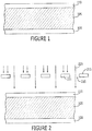
- FIGS 1-4 are cross-sectional views that illustrate the formation of metal-silicon carbide (SiC) ohmic contacts in light emitting devices according to some embodiments of the invention.
- SiC metal-silicon carbide
- the epitaxial layers 100 are formed on a front side of a SiC substrate 105.
- the epitaxial layers 100 may provide an active region of a light emitting device and may be formed of a GaN based material, such as, InGaN, GaAlInN or the like.
- a metal layer 110 is formed on a back side of the SiC substrate 105 opposite the epitaxial layer 100.
- the SiC substrate 105 can be any type of SiC material used to form light emitting devices such as 4H or 6H SiC.
- the metal layer 110 can be formed to a thickness of about 400 angstroms to about 1100 angstroms.
- the metal layer 110 can be a metal such as platinum, titanium, or preferably nickel.
- laser light 225 is impinged on corresponding interface locations of the metal layer 110 and the SiC substrate 105 through openings 220 in a mask 215. Some of the laser light 225 is blocked by the mask 215 from impinging on other interface locations of the metal layer 110 and the SiC substrate 105.
- interface locations 330 where the laser light 225 impinges the metal layer 110 and the SiC substrate 105 are annealed to form a metal-SiC material thereat.
- the metal-SiC material at the interface location is formed by the laser light 225 heating the metal and SiC to create a silicide of the metal.
- the other interface locations of the SiC substrate 105 and metal layer 110 that are blocked by the mask 215 are not annealed so that the metal-SiC material is not formed.
- portions of the metal layer 110 that are not annealed by the laser light 225 are removed, using, for example in the case of a nickel metal layer 110, a solution of HNO 3 :3H 2 O or HCL and H 2 O. Removal of the unannealed portions of the metal layer 110 exposes annealed metal-SiC ohmic contacts 435a-435d.
- the annealed metal-SiC ohmic contacts are formed by annealing interface locations of the metal layer 110 and the SiC substrate 105 whereas annealing of other locations on the substrate 105 is avoided by blocking the laser light from impinging on corresponding locations of the substrate.
- FIGS 5-7 are cross-sectional views that illustrate methods of forming metal-SiC ohmic contacts according to some embodiments of the invention.
- laser light 525 is impinged on the metal layer 110 according to a predetermined pattern. That is, some interface locations of the metal layer 110 and the underlying substrate 105 are impinged by the laser light 525 whereas other locations are not impinged by the laser light 525.
- the laser light 525 is impinged on the metal layer 110/substrate 105 by moving a laser beam above the metal layer 110 and activating/deactivating the laser to produce the laser light 525 according to the desired pattern.
- the laser beam may be activated/de-activated by pulsing the laser on/off or by modulating the laser beam to form the metal-SiC material where desired and to avoid the formation of the metal-SiC material otherwise.
- the laser beam can be moved in discreet steps according to the pattern whereas in other embodiments according to the invention, the laser beam is moved continuously and activated/deactivated at the appropriate intervals according to the pattern. It will be further understood that the laser beam can be "moved” by, for example, moving a mirror above the metal layer 110 to reflect the laser beam. Alternatively, the laser that generates the laser beam may be moved above the metal layer.
- the substrate can be moved beneath a "fixed" laser beam.
- the substrate can be moved in increments of the mask pitch and stopped at each location where the laser is activated for a number of pulses (or duration) at each location.
- a 1.8mm x 1.8mm field is used for a 6 x 6 array of 300um pitch die.
- the substrate can be moved beneath a fixed beam continuously along one axis, with activation of the laser beam being synchronized at every die pitch, which may vary by device.
- the number of pulses delivered to each site can be based on the number of die positions in the mask along the axis along which the substrate is moved.
- Figure 28 illustrates an exemplary laser mask through which laser light can be projected to anneal metal-SiC ohmic contacts according to some embodiments according to the invention.
- the interface locations of the metal layer 110 and the substrate 105 that are impinged by the laser light 525 are annealed to form a metal-SiC material 630 thereat. It will be understood that the other interface locations 631 upon which laser light 525 does not impinge remain unannealed.
- the unannealed portions of the metal layer 110 are removed using, for example an etching solution described above in reference to Figure 4 , to expose annealed metal-SiC ohmic contacts 735a-d.
- the annealed metal-SiC ohmic contacts are formed by impinging laser light at interface locations of the metal layer and the underlying SiC substrate according to a pattern. Annealing of other interface locations of the metal layer and the SiC substrate can be prevented by avoiding impinging the laser light on those corresponding portions of the metal layer and substrate.
- Figures 8-11 are cross-sectional views illustrating methods of forming metal-SiC ohmic contacts in light emitting devices according to some embodiments of the invention.
- a metal layer 110 is formed on a SiC substrate 105 opposite an epitaxial layer(s) 100.
- the metal layer 110 is patterned, using for example a lift-off or etching process, and portions thereof are removed so that portions of the metal layer 940a-940d remain on the substrate 105 having exposed portions of the substrate therebetween, as shown in Figure 9 . Accordingly, the remaining portions 940a-d of the metal layer 110 include interface locations with the underlying SiC substrate 105.
- laser light 1025 is impinged on the remaining portions 940a-d of the metal layer 110 and on the exposed portions of the SiC substrate 105 therebetween.
- the laser light 1025 anneals the remaining portions 940a-940d of the metal layer 110 to form annealed metal-SiC ohmic contacts 1135a-1135d on the substrate according to the pattern described above in reference to Figure 9 .
- the metal-SiC ohmic contacts are annealed by forming remaining metal portions from the metal layer according to a pattern and laser light is impinged upon both the remaining metal portions and the exposed SiC substrate so that the formation of the metal-SiC material is avoided in locations other than those corresponding to the remaining metal portions.
- the laser light 1025 should preferably not damage the boundaries of the metal-SiC ohmic contacts 1135a-1135d that are formed as described above.
- laser light 105 that impinges on the exposed portions of the SiC substrate 105 could damage the adjacent metal-SiC ohmic contacts 1135a-1135d.
- the ohmic contacts can include opposing metal-SiC ohmic contact boundaries near or at the outer edges of where the laser light impinges the interface of the metal and SiC substrate.
- the eradication of the metal-SiC ohmic contacts may be avoided by, for example, reducing the power of the laser light 1025 adjacent to the metal-SiC ohmic contacts.
- the wavelength of the laser light may be changed to avoid eradicating the adjacent metal-SiC ohmic contacts.
- Figures 12-17 are cross-sectional views that illustrate methods of forming annealed SiC ohmic contacts according to further embodiments of the invention.
- a layer of photoresist pattern 1245 is formed on the SiC substrate 105 according to a pattern so that portions of the substrate 105 remain covered by the photoresist 1245 whereas other portions of the SiC substrate 105 are exposed.
- a metal layer 1350 is formed on the photoresist pattern 1245 separated from the underlying SiC substrate 105 and on the exposed portions of the substrate 105 to define interface locations of the metal 1350 and the SiC substrate 105.
- laser light 1425 is impinged upon interface locations 1460 on the exposed portions of the SiC substrate 105.
- the laser light 1425 anneals the metal 1350 on the exposed portions of the SiC substrate 105 at the interface locations 1460 so that a metal-SiC material 1535a-d is formed thereat as shown in Figure 15 .
- the laser light 1425 may also be impinged upon the metal layer 1350 on the photoresist pattern 1245, however, the metal layer 1350 and the photoresist pattern 1245 may be damaged by the laser light 1425.
- an overlay 1665 is formed on the metal on the photoresist pattern 1245 and on the metal-SiC (SiC) material 1535a-1535d.
- the photoresist pattern 1245 and the metal 1350 thereon can be removed using a lift-off process including, for example, etching the photoresist pattern to remove the photoresist, the metal and overlay thereon as shown in Figure 17 .
- the laser light 1425 described above in reference to Figure 14 can be impinged subsequent to formation of the overlay pattern 1665 illustrated in Figure 16 .
- the overlay 1665 and the metal 1350 located on the photoresist pattern 1245 may be removed in separate steps rather than together as described above in reference to Figure 16 .
- Figures 18-20 are cross-sectional views illustrating the formation of metal-silicon carbide ohmic contacts in light emitting devices according to further embodiments of the invention.
- laser light 2525 is impinged on a metal 2510/SiC substrate 2505 in a blanket pattern to form an annealed metal-SiC layer 2660.
- Portions of the annealed metal-SiC layer 2660 are removed so that the remaining portions of the annealed metal-SiC layer 2660 form the metal-SiC ohmic contacts as shown in Figure 20 .
- the removal of portions of the metal layer can be performed using, for example, Reactive Ion Etching and photolithography techniques known to those skilled in the art.
- the metal-SiC ohmic contacts according to some embodiments of the invention can be formed using a blanket anneal via the laser light whereas annealing can be avoided by removing portions of the metal according to a pattern.
- Figures 21 and 22 are cross-sectional views that illustrate light emitting devices including metal-SiC (SiC) ohmic contacts formed according to embodiments of the invention.
- Figure 21 illustrates an annealed metal-SiC ohmic contact 1835 on a beveled edge SiC substrate 1805 opposite a stack of n/p type epitaxial layers 1800.
- the reduced thickness of the substrate 1805 may allow a saw tip to eliminate an upper portion of the substrate 1805 when the wafer is diced.
- the formation of such beveled edge devices is described, for example, in the U.S. Patent No. 5,087,949 , the disclosure of which is incorporated herein by reference in its entirety.
- Figure 22 illustrates a straight cut light emitting device including an annealed metal-SiC ohmic contact formed according to embodiments of the invention.
- an annealed metal-SiC ohmic contact 1935 is located on a substrate 1905 opposite a stack of n/p type epitaxially formed layers 1900.
- the structures shown in Figures 21 can produce higher light output and higher light extraction.
- the structure of Figure 21 may promote more conformal phosphor coatings to promote white light conversion efficiency due to the reduced thickness.
- Figure 23 is a schematic plan view of a wafer 2080 having been annealed as described above in reference to Figures 1-20 .
- pattern lines 2081 represent a laser light pattern used to anneal the metal-SiC ohmic contacts thereon according to some embodiments of the invention.
- the light can be impinged upon a metal layer on the wafer 2080 according to the pattern lines 2081.
- the pattern lines 2081 may be generated according by activating and deactivated the laser light according to a pattern or impinged on the substrate through openings in a mask.
- the light may be impinged upon a substrate having a photoresist pattern and a metal thereon.
- FIG 24 is a detailed view of a metal-SiC ohmic contact according to some embodiments of the invention.
- a metal-SiC ohmic contact 2100 includes opposing metal-SiC ohmic contact boundaries 2101, 2102 having a non-ohmic contact region 2103 therebetween.
- the metal-SiC material is formed proximate at the boundaries of where the laser light impacts the interface location.
- the ohmic contact boundaries 2101 and 2102 define an outer area where the laser light has impinged at the interface location of the metal layer in the SiC substrate.
- the ohmic contact boundaries 2101 and 2102 define the annealed metal-SiC ohmic contact where the non-ohmic contact region 2103 is included between the opposing ohmic contact boundaries 2101, 2102. It will be understood that the non-ohmic contact region, 2103 is also impinged by the laser light that anneals the interface location to form a metal-SiC at the opposing ohmic contact boundaries 2101, 2102. It will also be understood that the shape of the opposing ohmic contact boundaries 2101, 2102 can vary with the properties of the laser light used.
- the laser light may be de-focused to provide the un-even contours shown in Figure 24 or focused to provide contours that are relatively narrow and relatively even in width compared to those shown in Figure 24 . It will be understood, however, that the un-even contours shown in Figure 24 are exemplary in nature and are not limited to those illustrated.
- some edges in the laser mask can include features that measure less than a resolution of a lens (e.g., about 2um) used to direct the laser light, which is sometime referred to as "softening" the edges of the mask.
- the softening of the edges can cause the energy of the laser light to be gradually reduced toward the edges of the image produced by the mask. Reducing the energy near the edges can increase the density of the feature edges produced by the laser light projected through the mask.
- Exemplary mask features are shown in Figure 29A.
- Figure 29B shows a detailed view of a portion of the edges of the mask shown in Figure 29A according to some embodiments according to the invention.
- Figure 25 is a simplified plan view showing a plurality of metal-SiC ohmic contacts 2200 that form an oblique angle with a side of the device 2270. It will be understood that each of the stripes included in the plurality of metal-SiC ohmic contacts 2200 include opposing metal-SiC ohmic contact boundaries and non-ohmic contact regions therebetween, as illustrated for example, in Figure 24 .
- Figure 26 is a simplified plan view of a plurality of metal-SiC ohmic contacts defining a striped circular pattern 2300 wherein the stripes are parallel to a side of the device 2370. It will be understood that each of the stripes in the pattern 2300 includes respective opposing metal-SiC ohmic contact boundaries and non-ohmic contact regions therebetween, as illustrated for example in Figure 24 .
- Figure 27 is a simplified plan view of a pattern of metal-SiC ohmic contacts defining a circular concentric ring pattern 2400. It will be understood that each of the rings in the pattern 2400 include metal-SiC opposing ohmic contact boundaries and non-ohmic contact regions therebetween, as illustrated for example in Figure 24 .
- the stripes or rings included in the metal-SiC ohmic contacts described above in reference to Figures 23-27 can be formed having various thicknesses and spacing therebetween.
- the stripes in the metal-SiC ohmic contacts can have a width of about 10 microns and a spacing therebetween of about 100 microns or 106 microns.
- the spacing between the stripes can be about 4 to about 5 microns where the stripes are arranged in a substantially circular pattern having a diameter of about 95 microns, as illustrated for example in Figure 26 , or the concentric rings illustrated in Figure 27 .
- the stripe patterns shown in Figures 25-27 are shown separately, the stripe patterns may be combined to form metal-SiC ohmic contacts as described herein.
- the laser light used to anneal the metal-SiC ohmic contacts described herein can be a laser light having a wavelength and intensity sufficient to form the metal-silicide material at the interface of the metal layer and the SiC substrate.
- laser annealing may be accomplished by impinging laser light having a wavelength of about 248 nanometers to about 308 nanometers at an energy of about 2.8 joules per square centimeter in a single pulse having a duration of about 30 nanoseconds.
- the laser light may have a wavelength of about 248 nanometers to about 308 nanometers and an energy of about 4.2 joules per square centimeter applied in about 5 pulses, each having a duration of about 30 nanoseconds.
- other wavelengths and energies may be used to provide annealing at the interface location of the metal layer and the SiC substrate via absorption of light including photon energies that are above the bandgap of the SiC substrate. It will be understood that pulse and/or continuous loop lasers may also be utilized.
- electron beam annealing may be used as an alternative to laser light. Accordingly, in each of the embodiments described above, an electron beam may be used to anneal the interface locations of the metal layer and the SiC substrate to form the metal-SiC material thereat. It will be understood that the metal-SiC ohmic contacts can be a contact for any SiC device and may be included on a SiC epitaxial layer.
Abstract
Description
- This application claims the benefit of
U.S. Provisional Application No. 60/495,189, filed August 14, 2003 U.S. Provisional Application No. 60/495,284, filed August 15, 2003 - This invention relates to microelectronic devices, and more particularly, to the fabrication of light emitting devices (LEDs) and LEDs so formed.
- It is known that the thickness of Silicon-carbide (SiC) substrates in SiC-based light emitting devices can affect the forward voltage needed to operate the devices at a given current level. For example, the SiC-based light emitting diode C450-CB230-E1000 available from Cree, Inc. has a substrate thickness of about 250 µm (+/- 25 µm) and has an associated forward operating voltage of about 3.5 volts at about 10 mA forward operating current. Moreover, reducing the thickness of the SiC substrate of an LED may reduce the forward voltage, which may yield reduced power consumption in such diodes.
- It is also known that many small electronic devices may incorporate individual devices having reduced thicknesses so that the overall thickness of the electronic device may be reduced. For example, manufacturers of cellular phones may use surface-mounted LED chips to reduce the thickness of the component used to backlight a display of the cellular phone. Accordingly, reducing the thickness of the SiC substrate may also allow the device to be used in these types of small electronic devices.
- It is known to form ohmic contacts on SiC at low/room temperature by, for example, implanting ions into a backside of a SiC wafer. However, if an implanted SiC substrate is thinned prior to formation of ohmic contacts, the doped region may be removed during the thinning, which may make the implant superfluous. Accordingly, metals deposited to form ohmic contacts may not have ohmic properties when deposited on the substrate as the implant may be performed in a later step. Ion implantation for the formation of ohmic contacts is discussed, for example, in
U.S. Patent Application Serial Nos. 09/787,189 and10/003,331 - It is also known to form metal ohmic contacts by depositing a metal, such as nickel, and annealing the metal at a high temperature (such as temperatures greater than 900°C). High temperature annealing may damage epitaxial layers of gallium nitride based materials included on the SiC substrate. Accordingly, there is a need for improved methods for forming ohmic contacts to substrates of materials such as SiC, GaN, InGaN or the like.
-
-
Figures 1-4 are cross-sectional views illustrating the formation of metal-silicon carbide ohmic contacts in light emitting devices according to some embodiments of the invention. -
Figures 5-7 are cross-sectional views illustrating the formation of metal-silicon carbide ohmic contacts in light emitting devices according to further embodiments of the invention. -
Figures 8-11 are cross-sectional views illustrating the formation of metal-silicon carbide ohmic contacts in light emitting devices according to further embodiments of the invention. -
Figures 12-17 are cross-sectional views illustrating the formation of metal-silicon carbide ohmic contacts in light emitting devices according to further embodiments of the invention. -
Figures 18-20 are cross-sectional views illustrating the formation of metal-silicon carbide ohmic contacts in light emitting devices according to further embodiments of the invention. -
Figures 21 and 22 are cross-sectional views of metal-silicon carbide ohmic contacts in light emitting devices formed according to some embodiments of the invention. -
Figure 23 is a schematic plan view of a silicon carbide substrate subject to laser annealing according to some embodiments of the invention. -
Figure 24 is a simplified schematic view of a metal-silicon carbide ohmic contact including respective opposing ohmic contact boundaries according to some embodiments of the invention. -
Figure 25 is a simplified schematic plan view of a plurality of metal-silicon carbide ohmic contacts defining an oblique striped pattern according to some embodiments of the invention. -
Figure 26 is a simplified schematic plan view of a plurality of metal-silicon carbide ohmic contacts defining a striped circular pattern according to some embodiments of the invention. -
Figure 27 is a simplified schematic plan view of a plurality of metal-silicon carbide ohmic contacts defining a ringed circular pattern according to some embodiments of the invention. -
Figure 28 is an exemplary laser mask through which laser light can be projected to anneal metal-SiC ohmic contacts according to some embodiments according to the invention. -
Figure 29A is an exemplary mask having "softened" edge features according to some embodiments according to the invention. -
Figure 29B is a detailed view of a portion shown inFigure 29A . - Embodiments according to the invention can provide localized annealing of metal-silicon carbide ohmic contacts in semiconductor devices and devices so formed. Pursuant to these embodiments, a contact can be formed by forming a metal on a Silicon Carbide (SiC) layer and annealing an interface location of the metal and the SiC layer to form a metal-SiC material thereat and avoiding annealing at a location on the SiC layer to avoid forming the metal-SiC material thereat. In some embodiments according to the invention, the layer can be a SiC substrate.
- In some embodiments according to the invention, the annealing can include annealing at the interface location and annealing according to a pattern to avoid annealing at the location. In some embodiments according to the invention, the interface location can be a first interface location and the location on the SiC substrate can be a second interface location of the metal and the SiC substrate. The annealing can include impinging laser light through an opening in a mask layer onto the metal layer at the first interface location and blocking the laser light with the mask layer opposite the second interface location to avoid annealing at the second interface location.
- In some embodiments according to the invention, the annealing can include activating a laser opposite the interface location to impinge laser light onto the metal layer at the interface location and de-activating the laser opposite the location to avoid annealing at the location. In some embodiments according to the invention, forming the metal can include forming the metal on the SiC substrate to form the location spaced-apart from the SiC substrate.
- In some embodiments according to the invention, the metal can be formed in a pattern to expose a portion of the SiC substrate at the location and the annealing can include activating a laser opposite the interface location to impinge laser light onto the metal layer at the interface location. Activation of the laser can be maintained opposite the location.
- In some embodiments according to the invention, the metal-SiC material at the interface location can be a metal ohmic contact on a back side of the substrate opposite a front side of the substrate having an epitaxial layer thereon. In some embodiments according to the invention, the annealing can include impinging laser light on the interface location to form at least one ohmic contact including opposing ohmic contact boundaries having a non-ohmic contact region therebetween.
- In some embodiments according to the invention, the at least one ohmic contact can be a plurality of ohmic contacts including respective opposing ohmic contact boundaries defining a striped pattern forming an oblique angle with a side of the device. In some embodiments according to the invention, the at least one ohmic contact can include a plurality of ohmic contacts including respective opposing ohmic contact boundaries defining a striped pattern parallel to a side of the device.
- In some embodiments according to the invention, the at least one ohmic contact can include a plurality of ohmic contacts including respective opposing ohmic contact boundaries defining a circular pattern. In some embodiments according to the invention, the interface location can be a first interface location and the location on the SiC substrate comprises a second interface location of the metal and the SiC substrate. Annealing can include impinging an electron beam on the interface location and blocking the electron beam from impinging the second interface location.
- In some embodiments according to the invention, forming a contact for a light emitting device can include forming a metal on a Silicon Carbide (SiC) substrate and laser annealing interface locations of the metal and the SiC substrate according to a pattern to form a metal-SiC material thereat corresponding to the pattern. In some embodiments according to the invention, forming the metal can include forming a blanket metal on the substrate. The laser annealing can include impinging laser light on the interface locations through openings in a mask, that defines the pattern, to form the metal-SiC material thereat. The laser light can be blocked with the mask opposite other interface locations of the metal and the SiC substrate.
- In some embodiments according to the invention, forming the metal can include forming a blanket metal on the substrate, wherein laser annealing can include activating a laser opposite the interface locations, according to the pattern, to impinge laser light onto the blanket metal layer at the interface location. The laser can be deactivated opposite other interface locations to avoid annealing at the other locations.
- In some embodiments according to the invention, the metal can be nickel, platinum, or titanium. In some embodiments according to the invention, laser annealing can include impinging laser light on the interface locations at an energy and wavelength sufficient to form a silicide of the metal and the SiC substrate.
- In some embodiments according to the invention, the SiC substrate can be 6H SiC, wherein laser annealing can include impinging laser light having a wavelength of about 248 nanometers to about 308 nanometers at an energy of about 2.8 joules/cm2 in a single pulse having a duration of about 30 nanoseconds. In some embodiments according to the invention, the SiC substrate can be 4H SiC, wherein laser annealing can include impinging laser light having a wavelength of about 248 nanometers to about 308 nanometers at an energy of about 4.2 joules/cm2 in about five pulses each having a duration of about 30 nanoseconds. In some embodiments according to the invention, the laser light can be photon energies above a bandgap of the SiC substrate. In some embodiments according to the invention, the laser light can be pulsed or continuous wave laser light.
- In some embodiments according to the invention, a contact for a light emitting device can include forming a metal on a Silicon Carbide (SiC) layer according to a pattern so that portions of the layer are exposed. Laser light can be impinged on the exposed portions of the SiC layer and on interface locations of the metal and the Si-C layer to form a metal-SiC material thereat corresponding to the pattern. In some embodiments according to the invention, the layer can be a SiC substrate.
- In some embodiments according to the invention, the metal can be nickel, platinum, or titanium. In some embodiments according to the invention, the laser annealing can include impinging laser light on the interface locations at an energy and wavelength sufficient to form a silicide of the metal and the SiC substrate.
- In some embodiments according to the invention, the SiC substrate can be 6H SiC, wherein the laser annealing can include impinging laser light having a wavelength of about 248 nanometers to about 308 nanometers at an energy of about 2.8 joules/cm2 in a single pulse having a duration of about 30 nanoseconds.
- In some embodiments according to the invention, the SiC substrate can be 4H SiC, wherein the laser annealing can include impinging laser light having a wavelength of about 248 nanometers to about 308 nanometers at an energy of about 4.2 joules/cm2 in about five pulses each having a duration of about 30 nanoseconds.
- In some embodiments according to the invention, the laser light can include photon energies above a bandgap of the SiC substrate. In some embodiments according to the invention, the laser light can be pulsed or continuous wave laser light.
- In some embodiments according to the invention, a method of forming an ohmic contact for a semiconductor device can include forming a photoresist on a SiC layer according to a pattern to expose first portions of the SiC layer and to cover second portions of the substrate. A blanket metal can be formed on the first portions and on the photoresist. Laser light can be impinged on interface locations of the blanket metal and the SiC layer corresponding to the first portions to form a metal-SiC material thereat, whereas impinging laser light on the blanket metal corresponding to the second portions can be avoided.
- In some embodiments according to the invention, the method can further include removing metal from the photoresist so that metal-SiC material remains. An overlay can be formed on the metal-SiC material and the photoresist can be removed from the SiC substrate. In some embodiments according to the invention, the method can further include forming an overlay on the metal-SiC material and on the photoresist and removing the photoresist from the SiC layer.
- In further embodiments according to the invention, the method can further include lifting-off the photoresist and the metal thereon leaving the metal-SiC material. An overlay can be formed on the metal-SiC material. In some embodiments according to the invention, the metal can be nickel, platinum, or titanium. In some embodiments according to the invention, the laser annealing can include impinging laser light on the interface locations at an energy and wavelength sufficient to form a silicide of the metal and the SiC substrate.
- In some embodiments according to the invention, forming a contact can include impinging laser light on an interface location between a metal and a Silicon Carbide (SiC) layer to form a metal-SiC material to provide at least one ohmic contact on the device including opposing ohmic contact boundaries having a non-ohmic contact region therebetween.
- In some embodiments according to the invention, a light emitting device (LED) can include at least one metal-Silicon Carbide (SiC) ohmic contact on a SiC layer, the at least one metal-SiC ohmic contact including opposing ohmic contact boundaries having a non-ohmic contact region therebetween.
- In some embodiments according to the invention, the opposing ohmic contact boundaries are separated by about 10 um. In some embodiments according to the invention, the at least one ohmic contact can include a plurality of ohmic contacts including respective opposing ohmic contact boundaries defining stripes in a striped pattern forming oblique angles with a side of the device.
- In some embodiments according to the invention, the stripes are separated about 106 um. In some embodiments according to the invention, the at least one ohmic contact can include a plurality of ohmic contacts including respective opposing ohmic contact boundaries defining stripes a striped pattern parallel to a side of the device.
- In some embodiments according to the invention, the striped pattern defines a substantially circular shape having a diameter of about 95 um, wherein the stripes are separated by distance of about 4.0 um to about 5.0 um. In some embodiments according to the invention, the at least one ohmic contact can include a plurality of ohmic contacts including respective opposing ohmic contact boundaries defining rings of a concentric circular pattern. In some embodiments according to the invention, the rings are separated by a distance of about 4.0 um to about 5.0 um.
- In some embodiments according to the invention, a method of forming an ohmic contact for a semiconductor device can include forming a metal on a Silicon Carbide (SiC) layer and laser annealing the metal and the SiC layer to form a metal-SiC material at interface locations of the metal and the SiC layer. Portions of the metal-SiC material can be removed to expose the SiC layer according to a pattern to provide at least one ohmic contact on the semiconductor device.
- The present invention now will be described more fully hereinafter with reference to the accompanying drawings, in which embodiments of the invention are shown. However, this invention should not be construed as limited to the embodiments set forth herein. Rather, these embodiments are provided so that this disclosure will be thorough and complete, and will fully convey the scope of the invention to those skilled in the art. In the drawings, the thickness of layers and regions are exaggerated for clarity. Like numbers refer to like elements throughout. As used herein the term "and/or" includes any and all combinations of one or more of the associated listed items.
- The terminology used herein is for the purpose of describing particular embodiments only and is not intended to be limiting of the invention. As used herein, the singular forms "a", "an" and "the" are intended to include the plural forms as well, unless the context clearly indicates otherwise. It will be further understood that the terms "comprises" and/or "comprising," when used in this specification, specify the presence of stated features, integers, steps, operations, elements, and/or components, but do not preclude the presence or addition of one or more other features, integers, steps, operations, elements, components, and/or groups thereof.
- It will be understood that when an element such as a layer, region or substrate is referred to as being "on" or extending "onto" another element, it can be directly on or extend directly onto the other element or intervening elements may also be present. In contrast, when an element is referred to as being "directly on" or extending "directly onto" another element, there are no intervening elements present. It will also be understood that when an element is referred to as being "connected" or "coupled" to another element, it can be directly connected or coupled to the other element or intervening elements may be present. In contrast, when an element is referred to as being "directly connected" or "directly coupled" to another element, there are no intervening elements present. Like numbers refer to like elements throughout the specification.
- It will be understood that, although the terms first, second, etc. may be used herein to describe various elements, components, regions, layers and/or sections, these elements, components, regions, layers and/or sections should not be limited by these terms. These terms are only used to distinguish one element, component, region, layer or section from another region, layer or section. Thus, a first element, component, region, layer or section discussed below could be termed a second element, component, region, layer or section without departing from the teachings of the present invention.
- Furthermore, relative terms, such as "lower" or "bottom" and "upper" or "top," may be used herein to describe one element's relationship to another elements as illustrated in the Figures. It will be understood that relative terms are intended to encompass different orientations of the device in addition to the orientation depicted in the Figures. For example, if the device in the Figures is turned over, elements described as being on the "lower" side of other elements would then be oriented on "upper" sides of the other elements. The exemplary term "lower", can therefore, encompasses both an orientation of "lower" and "upper," depending of the particular orientation of the figure. Similarly, if the device in one of the figures is turned over, elements described as "below" or "beneath" other elements would then be oriented "above" the other elements. The exemplary terms "below" or "beneath" can, therefore, encompass both an orientation of above and below.
- Embodiments of the present invention are described herein with reference to cross-section (and/or plan view) illustrations that are schematic illustrations of idealized embodiments of the present invention. As such, variations from the shapes of the illustrations as a result, for example, of manufacturing techniques and/or tolerances, are to be expected. Thus, embodiments of the present invention should not be construed as limited to the particular shapes of regions illustrated herein but are to include deviations in shapes that result, for example, from manufacturing. For example, an etched region illustrated or described as a rectangle will, typically, have rounded or curved features. Thus, the regions illustrated in the figures are schematic in nature and their shapes are not intended to illustrate the precise shape of a region of a device and are not intended to limit the scope of the present invention.
- Unless otherwise defined, all terms (including technical and scientific terms) used herein have the same meaning as commonly understood by one of ordinary skill in the art to which this invention belongs. It will be further understood that terms, such as those defined in commonly used dictionaries, should be interpreted as having a meaning that is consistent with their meaning in the context of the relevant art and will not be interpreted in an idealized or overly formal sense unless expressly so defined herein. It will also be appreciated by those of skill in the art that references to a structure or feature that is disposed "adjacent" another feature may have portions that overlap or underlie the adjacent feature.
- As used herein the term "ohmic contact" refers to contacts where an impedance associated therewith is substantially given by the relationship of Impedance = V/I, where V is a voltage across the contact and I is the current, at substantially all expected operating frequencies (i.e., the impedance associated with the ohmic contact is substantially the same at all operating frequencies). For example, in some embodiments according to the invention, an ohmic contact can be a contact with a specific contact resistivity of less than about 10 e -03 ohm-cm2 and, in some embodiments less than about 10 e -04 ohm-cm2. Thus, a contact that is rectifying or that has a high specific contact resistivity, for example, a specific contact resistivity of greater than about 10 e -03 ohm-cm2, is not an ohmic contact as that term is used herein. As used herein, a "metal-SiC material" includes mixtures containing a metal and Silicon Carbide fused together or dissolving into each other when annealed. It will also be understood that, for example, a Ni-SiC material can be a mixture (or alloy) of nickel and silicon carbide when annealed so that a Ni-silicide is formed.
- As described herein in greater detail, embodiments according to the invention may provide methods of annealing interface locations of a metal and a silicon carbide substrate to form a metal-silicon carbide material thereat and avoid annealing other locations on the silicon carbide substrate so as to avoid forming a metal silicon carbide material. It will be understood that the interface locations where the metal-silicon carbide material is formed can include boundaries at or near the outer area where the laser light impinges the metal and the substrate. For example, as described in further detail herein in reference to
Figure 21 , when the laser light is impinged on the interface, a metal-SiC ohmic contact is formed which includes opposing ohmic contact boundaries and a non-ohmic area therebetween (where for the laser light has directly impinged) a metal-SiC material is formed at an interface location - Annealing at one location with, for example a laser beam, while avoiding annealing at another location on the silicon carbide substrate may avoid the type of damage caused by a conventional rapid thermal anneal to an epitaxial layer. For example, in some embodiments according to the invention, metal-silicon carbide ohmic contacts can be formed by annealing the interface locations on the substrate using laser light while avoiding annealing other locations on the substrate (by masking or modulating the laser light) after an epitaxial layer has been formed on the front side of the substrate.
-
Figures 1-4 are cross-sectional views that illustrate the formation of metal-silicon carbide (SiC) ohmic contacts in light emitting devices according to some embodiments of the invention. In particular, one or moreepitaxial layers 100 are formed on a front side of aSiC substrate 105. Theepitaxial layers 100 may provide an active region of a light emitting device and may be formed of a GaN based material, such as, InGaN, GaAlInN or the like. Ametal layer 110 is formed on a back side of theSiC substrate 105 opposite theepitaxial layer 100. It will be understood that theSiC substrate 105 can be any type of SiC material used to form light emitting devices such as 4H or 6H SiC. It will also be understood that themetal layer 110 can be formed to a thickness of about 400 angstroms to about 1100 angstroms. Themetal layer 110 can be a metal such as platinum, titanium, or preferably nickel. - As shown in
Figure 2 ,laser light 225 is impinged on corresponding interface locations of themetal layer 110 and theSiC substrate 105 throughopenings 220 in amask 215. Some of thelaser light 225 is blocked by themask 215 from impinging on other interface locations of themetal layer 110 and theSiC substrate 105. - As shown in
Figure 3 ,interface locations 330 where thelaser light 225 impinges themetal layer 110 and theSiC substrate 105 are annealed to form a metal-SiC material thereat. In some embodiments according to the invention, the metal-SiC material at the interface location is formed by thelaser light 225 heating the metal and SiC to create a silicide of the metal. Conversely, the other interface locations of theSiC substrate 105 andmetal layer 110 that are blocked by themask 215 are not annealed so that the metal-SiC material is not formed. - According to
Figure 4 , portions of themetal layer 110 that are not annealed by thelaser light 225 are removed, using, for example in the case of anickel metal layer 110, a solution of HNO3:3H2O or HCL and H2O. Removal of the unannealed portions of themetal layer 110 exposes annealed metal-SiC ohmic contacts 435a-435d. As described above, in some embodiments according to the invention, the annealed metal-SiC ohmic contacts are formed by annealing interface locations of themetal layer 110 and theSiC substrate 105 whereas annealing of other locations on thesubstrate 105 is avoided by blocking the laser light from impinging on corresponding locations of the substrate. -
Figures 5-7 are cross-sectional views that illustrate methods of forming metal-SiC ohmic contacts according to some embodiments of the invention. As shown inFigure 5 ,laser light 525 is impinged on themetal layer 110 according to a predetermined pattern. That is, some interface locations of themetal layer 110 and theunderlying substrate 105 are impinged by thelaser light 525 whereas other locations are not impinged by thelaser light 525. In some embodiments according to the invention, thelaser light 525 is impinged on themetal layer 110/substrate 105 by moving a laser beam above themetal layer 110 and activating/deactivating the laser to produce thelaser light 525 according to the desired pattern. It will be understood that the laser beam may be activated/de-activated by pulsing the laser on/off or by modulating the laser beam to form the metal-SiC material where desired and to avoid the formation of the metal-SiC material otherwise. - Regarding "moving" the laser beam described above, it will be understood that in some embodiments according to the invention, the laser beam can be moved in discreet steps according to the pattern whereas in other embodiments according to the invention, the laser beam is moved continuously and activated/deactivated at the appropriate intervals according to the pattern. It will be further understood that the laser beam can be "moved" by, for example, moving a mirror above the
metal layer 110 to reflect the laser beam. Alternatively, the laser that generates the laser beam may be moved above the metal layer. - In still other embodiments according to the invention, the substrate can be moved beneath a "fixed" laser beam. For example, the substrate can be moved in increments of the mask pitch and stopped at each location where the laser is activated for a number of pulses (or duration) at each location. In some embodiments according to the invention, a 1.8mm x 1.8mm field is used for a 6 x 6 array of 300um pitch die. Alternatively, the substrate can be moved beneath a fixed beam continuously along one axis, with activation of the laser beam being synchronized at every die pitch, which may vary by device. The number of pulses delivered to each site can be based on the number of die positions in the mask along the axis along which the substrate is moved. The wafer may then be indexed by the mask pitch along the non-scanned axis, whereupon the scanning can be repeated.
Figure 28 illustrates an exemplary laser mask through which laser light can be projected to anneal metal-SiC ohmic contacts according to some embodiments according to the invention. - As shown in
Figure 6 , the interface locations of themetal layer 110 and thesubstrate 105 that are impinged by thelaser light 525 are annealed to form a metal-SiC material 630 thereat. It will be understood that theother interface locations 631 upon whichlaser light 525 does not impinge remain unannealed. According toFigure 7 , the unannealed portions of themetal layer 110 are removed using, for example an etching solution described above in reference toFigure 4 , to expose annealed metal-SiC ohmic contacts 735a-d. Accordingly, in some embodiments according to the invention, the annealed metal-SiC ohmic contacts are formed by impinging laser light at interface locations of the metal layer and the underlying SiC substrate according to a pattern. Annealing of other interface locations of the metal layer and the SiC substrate can be prevented by avoiding impinging the laser light on those corresponding portions of the metal layer and substrate. -
Figures 8-11 are cross-sectional views illustrating methods of forming metal-SiC ohmic contacts in light emitting devices according to some embodiments of the invention. InFigure 8 , ametal layer 110 is formed on aSiC substrate 105 opposite an epitaxial layer(s) 100. Themetal layer 110 is patterned, using for example a lift-off or etching process, and portions thereof are removed so that portions of themetal layer 940a-940d remain on thesubstrate 105 having exposed portions of the substrate therebetween, as shown inFigure 9 . Accordingly, the remainingportions 940a-d of themetal layer 110 include interface locations with theunderlying SiC substrate 105. - As shown in
Figure 10 ,laser light 1025 is impinged on the remainingportions 940a-d of themetal layer 110 and on the exposed portions of theSiC substrate 105 therebetween. Thelaser light 1025 anneals the remainingportions 940a-940d of themetal layer 110 to form annealed metal-SiC ohmic contacts 1135a-1135d on the substrate according to the pattern described above in reference toFigure 9 . Accordingly, in some embodiments according to the invention, the metal-SiC ohmic contacts are annealed by forming remaining metal portions from the metal layer according to a pattern and laser light is impinged upon both the remaining metal portions and the exposed SiC substrate so that the formation of the metal-SiC material is avoided in locations other than those corresponding to the remaining metal portions. - It will be understood by those skilled in the art, given the benefit of this disclosure, that the
laser light 1025 should preferably not damage the boundaries of the metal-SiC ohmic contacts 1135a-1135d that are formed as described above. In particular, if un-addressed,laser light 105 that impinges on the exposed portions of theSiC substrate 105 could damage the adjacent metal-SiC ohmic contacts 1135a-1135d. As described in reference toFigure 24 , the ohmic contacts can include opposing metal-SiC ohmic contact boundaries near or at the outer edges of where the laser light impinges the interface of the metal and SiC substrate. In some embodiments according to the invention, the eradication of the metal-SiC ohmic contacts may be avoided by, for example, reducing the power of thelaser light 1025 adjacent to the metal-SiC ohmic contacts. In some embodiments according to the invention, the wavelength of the laser light may be changed to avoid eradicating the adjacent metal-SiC ohmic contacts. -
Figures 12-17 are cross-sectional views that illustrate methods of forming annealed SiC ohmic contacts according to further embodiments of the invention. A layer ofphotoresist pattern 1245 is formed on theSiC substrate 105 according to a pattern so that portions of thesubstrate 105 remain covered by thephotoresist 1245 whereas other portions of theSiC substrate 105 are exposed. According toFigure 13 , ametal layer 1350 is formed on thephotoresist pattern 1245 separated from theunderlying SiC substrate 105 and on the exposed portions of thesubstrate 105 to define interface locations of themetal 1350 and theSiC substrate 105. - As shown in
Figure 14 ,laser light 1425 is impinged uponinterface locations 1460 on the exposed portions of theSiC substrate 105. Thelaser light 1425 anneals themetal 1350 on the exposed portions of theSiC substrate 105 at theinterface locations 1460 so that a metal-SiC material 1535a-d is formed thereat as shown inFigure 15 . In some alternative embodiments according to the invention, thelaser light 1425 may also be impinged upon themetal layer 1350 on thephotoresist pattern 1245, however, themetal layer 1350 and thephotoresist pattern 1245 may be damaged by thelaser light 1425. - According to
Figure 16 , anoverlay 1665 is formed on the metal on thephotoresist pattern 1245 and on the metal-SiC (SiC)material 1535a-1535d. Thephotoresist pattern 1245 and themetal 1350 thereon (including the corresponding portion of the overlay 1665) can be removed using a lift-off process including, for example, etching the photoresist pattern to remove the photoresist, the metal and overlay thereon as shown inFigure 17 . - It will be understood that in some embodiments according to the invention, the
laser light 1425 described above in reference toFigure 14 , can be impinged subsequent to formation of theoverlay pattern 1665 illustrated inFigure 16 . Furthermore, theoverlay 1665 and themetal 1350 located on thephotoresist pattern 1245 may be removed in separate steps rather than together as described above in reference toFigure 16 . -
Figures 18-20 are cross-sectional views illustrating the formation of metal-silicon carbide ohmic contacts in light emitting devices according to further embodiments of the invention. According toFigures 18 and 19 ,laser light 2525 is impinged on ametal 2510/SiC substrate 2505 in a blanket pattern to form an annealed metal-SiC layer 2660. Portions of the annealed metal-SiC layer 2660 are removed so that the remaining portions of the annealed metal-SiC layer 2660 form the metal-SiC ohmic contacts as shown inFigure 20 . It will be understood that the removal of portions of the metal layer can be performed using, for example, Reactive Ion Etching and photolithography techniques known to those skilled in the art. Accordingly, the metal-SiC ohmic contacts according to some embodiments of the invention can be formed using a blanket anneal via the laser light whereas annealing can be avoided by removing portions of the metal according to a pattern. -
Figures 21 and 22 are cross-sectional views that illustrate light emitting devices including metal-SiC (SiC) ohmic contacts formed according to embodiments of the invention. In particular,Figure 21 illustrates an annealed metal-SiC ohmic contact 1835 on a bevelededge SiC substrate 1805 opposite a stack of n/p type epitaxial layers 1800. The reduced thickness of thesubstrate 1805 may allow a saw tip to eliminate an upper portion of thesubstrate 1805 when the wafer is diced. The formation of such beveled edge devices is described, for example, in theU.S. Patent No. 5,087,949 , the disclosure of which is incorporated herein by reference in its entirety. -
Figure 22 illustrates a straight cut light emitting device including an annealed metal-SiC ohmic contact formed according to embodiments of the invention. In particular, an annealed metal-SiC ohmic contact 1935 is located on asubstrate 1905 opposite a stack of n/p type epitaxially formed layers 1900. The structures shown inFigures 21 can produce higher light output and higher light extraction. Furthermore, the structure ofFigure 21 may promote more conformal phosphor coatings to promote white light conversion efficiency due to the reduced thickness. -
Figure 23 is a schematic plan view of awafer 2080 having been annealed as described above in reference toFigures 1-20 . In particular,pattern lines 2081 represent a laser light pattern used to anneal the metal-SiC ohmic contacts thereon according to some embodiments of the invention. As described above, the light can be impinged upon a metal layer on thewafer 2080 according to the pattern lines 2081. Alternatively, thepattern lines 2081 may be generated according by activating and deactivated the laser light according to a pattern or impinged on the substrate through openings in a mask. Furthermore, the light may be impinged upon a substrate having a photoresist pattern and a metal thereon. -
Figure 24 is a detailed view of a metal-SiC ohmic contact according to some embodiments of the invention. In particular, a metal-SiC ohmic contact 2100 includes opposing metal-SiCohmic contact boundaries 2101, 2102 having anon-ohmic contact region 2103 therebetween. As appreciated by the present inventors, when laser light impinges the interface location of the SiC substrate and overlying metal layer, the metal-SiC material is formed proximate at the boundaries of where the laser light impacts the interface location. For example, as shown inFigure 24 , theohmic contact boundaries 2101 and 2102 define an outer area where the laser light has impinged at the interface location of the metal layer in the SiC substrate. - Therefore, in some embodiments according to the invention, the
ohmic contact boundaries 2101 and 2102 define the annealed metal-SiC ohmic contact where thenon-ohmic contact region 2103 is included between the opposingohmic contact boundaries 2101, 2102. It will be understood that the non-ohmic contact region, 2103 is also impinged by the laser light that anneals the interface location to form a metal-SiC at the opposingohmic contact boundaries 2101, 2102. It will also be understood that the shape of the opposingohmic contact boundaries 2101, 2102 can vary with the properties of the laser light used. For example, the laser light may be de-focused to provide the un-even contours shown inFigure 24 or focused to provide contours that are relatively narrow and relatively even in width compared to those shown inFigure 24 . It will be understood, however, that the un-even contours shown inFigure 24 are exemplary in nature and are not limited to those illustrated. - In still other embodiments according to the invention, some edges in the laser mask can include features that measure less than a resolution of a lens (e.g., about 2um) used to direct the laser light, which is sometime referred to as "softening" the edges of the mask. In particular, the softening of the edges can cause the energy of the laser light to be gradually reduced toward the edges of the image produced by the mask. Reducing the energy near the edges can increase the density of the feature edges produced by the laser light projected through the mask. Exemplary mask features are shown in
Figure 29A. Figure 29B shows a detailed view of a portion of the edges of the mask shown inFigure 29A according to some embodiments according to the invention. -
Figure 25 is a simplified plan view showing a plurality of metal-SiC ohmic contacts 2200 that form an oblique angle with a side of the device 2270. It will be understood that each of the stripes included in the plurality of metal-SiC ohmic contacts 2200 include opposing metal-SiC ohmic contact boundaries and non-ohmic contact regions therebetween, as illustrated for example, inFigure 24 . -
Figure 26 is a simplified plan view of a plurality of metal-SiC ohmic contacts defining a stripedcircular pattern 2300 wherein the stripes are parallel to a side of the device 2370. It will be understood that each of the stripes in thepattern 2300 includes respective opposing metal-SiC ohmic contact boundaries and non-ohmic contact regions therebetween, as illustrated for example inFigure 24 . -
Figure 27 is a simplified plan view of a pattern of metal-SiC ohmic contacts defining a circularconcentric ring pattern 2400. It will be understood that each of the rings in thepattern 2400 include metal-SiC opposing ohmic contact boundaries and non-ohmic contact regions therebetween, as illustrated for example inFigure 24 . - It will be understood that in some embodiments according to the invention, the stripes or rings included in the metal-SiC ohmic contacts described above in reference to
Figures 23-27 , can be formed having various thicknesses and spacing therebetween. For example, in some embodiments according to the invention, the stripes in the metal-SiC ohmic contacts can have a width of about 10 microns and a spacing therebetween of about 100 microns or 106 microns. In other embodiments according to the invention, the spacing between the stripes can be about 4 to about 5 microns where the stripes are arranged in a substantially circular pattern having a diameter of about 95 microns, as illustrated for example inFigure 26 , or the concentric rings illustrated inFigure 27 . It will also be understood that although the stripe patterns shown inFigures 25-27 are shown separately, the stripe patterns may be combined to form metal-SiC ohmic contacts as described herein. - It will be understood that the laser light used to anneal the metal-SiC ohmic contacts described herein can be a laser light having a wavelength and intensity sufficient to form the metal-silicide material at the interface of the metal layer and the SiC substrate. For example, in embodiments using 6H SiC as the substrate, laser annealing may be accomplished by impinging laser light having a wavelength of about 248 nanometers to about 308 nanometers at an energy of about 2.8 joules per square centimeter in a single pulse having a duration of about 30 nanoseconds. In other embodiments according to the invention where, for example, the SiC substrate is 4H SiC, the laser light may have a wavelength of about 248 nanometers to about 308 nanometers and an energy of about 4.2 joules per square centimeter applied in about 5 pulses, each having a duration of about 30 nanoseconds. In still other embodiments according to the invention, other wavelengths and energies may be used to provide annealing at the interface location of the metal layer and the SiC substrate via absorption of light including photon energies that are above the bandgap of the SiC substrate. It will be understood that pulse and/or continuous loop lasers may also be utilized.
- It will be also understood that electron beam annealing may be used as an alternative to laser light. Accordingly, in each of the embodiments described above, an electron beam may be used to anneal the interface locations of the metal layer and the SiC substrate to form the metal-SiC material thereat. It will be understood that the metal-SiC ohmic contacts can be a contact for any SiC device and may be included on a SiC epitaxial layer.
- Many alterations and modifications may be made by those having ordinary skill in the art, given the benefit of the present disclosure, without departing from the spirit and scope of the invention. Therefore, it must be understood that the illustrated embodiments have been set forth only for the purposes of example, and that it should not be taken as limiting the invention as defined by the following claims. The following claims are, therefore, to be read to include not only the combination of elements which are literally set forth but all equivalent elements for performing substantially the same function in substantially the same way to obtain substantially the same result. The claims are thus to be understood to include what is specifically illustrated and described above, what is conceptually equivalent, and also what incorporates the essential idea of the invention.
- The invention will now be described with reference to the following numbered clauses:
- 1. A method of forming an ohmic contact for a semiconductor device, comprising : forming a metal on a Silicon Carbide (SiC) layer; and annealing an interface location of the metal and the SiC layer to form a metal- SiC material thereat and avoiding annealing at a location on the SiC layer to avoid forming the metal-SiC material thereat.
- 2. A method according to Clause 1 wherein the SiC layer comprises a SiC substrate.
- 3. A method according to Clause 2 wherein annealing comprises: annealing at the interface location; and annealing according to a pattern to avoid annealing at the location.
- 4. A method according to Clause 2, wherein the interface location comprises a first interface location and the location on the SiC substrate comprises a second interface location of the metal and the SiC substrate, wherein annealing comprises: impinging laser light through an opening in a mask layer onto the metal layer at the first interface location and blocking the laser light with the mask layer opposite the second interface location to avoid annealing at the second interface location.
- 5. A method according to Clause 1 wherein annealing comprises: activating a laser opposite the interface location to impinge laser light onto the metal layer at the interface location; and de-activating the laser opposite the location to avoid annealing at the location.
- 6. A method according to Clause 2 wherein forming a metal comprises: forming the metal on the SiC substrate to form the location, wherein the location is spaced-apart from the SiC substrate.
- 7. A method according to Clause 2 wherein the metal is formed in a pattern to expose a portion of the SiC substrate at the location, wherein annealing comprises: activating a laser opposite the interface location to impinge laser light onto the metal layer at the interface location; and maintaining activation of the laser opposite the location.
- 8. A method according to Clause 2 wherein the metal-SiC material at the interface location comprises a metal ohmic contact on a back side of the substrate opposite a front side of the substrate having an epitaxial layer thereon.
- 9. A method according to Clause 1 wherein annealing comprises: impinging laser light on the interface location to form at least one ohmic contact including opposing ohmic contact boundaries having a non-ohmic contact region therebetween.
- 10. A method according to Clause 9 wherein the at least one ohmic contact comprises a plurality of ohmic contacts including respective opposing ohmic contact boundaries defining a striped pattern forming an oblique angle with a side of the device.
- 11. A method according to Clause 6 wherein the at least one ohmic contact comprises a plurality of ohmic contacts including respective opposing ohmic contact boundaries defining a striped pattern parallel to a side of the device.
- 12. A method according to Clause 6 wherein the at least one ohmic contact comprises a plurality of ohmic contacts including respective opposing ohmic contact boundaries defining a circular pattern.
- 13. A method according to Clause 2, wherein the interface location comprises a first interface location and the location on the SiC substrate comprises a second interface location of the metal and the SiC substrate, wherein annealing comprises: impinging an electron beam on the interface location and blocking the electron beam from impinging the second interface location.
- 14. A method of forming an ohmic contact for a semiconductor device, comprising: forming a metal on a Silicon Carbide (SiC) layer; and laser annealing interface locations of the metal and the SiC layer according to a pattern to form a metal-SiC material thereat corresponding to the pattern.
- 15. A method according to Clause 14 wherein the SiC layer comprises a SiC substrate.
- 16. A method according to Clause 15 wherein forming a metal comprises forming a blanket metal on the substrate, wherein laser annealing comprises: impinging laser light on the interface locations through openings in a mask, that defines the pattern, to form the metal-SiC material thereat; and blocking the laser light with the mask opposite other interface locations of the metal and the SiC substrate.
- 17. A method according to Clause 14 wherein forming a metal comprises forming a blanket metal on the substrate, wherein laser annealing comprises: activating a laser opposite the interface locations, according to the pattern, to impinge laser light onto the blanket metal layer at the interface location; and de-activating the laser opposite other interface locations to avoid annealing at the other locations.
- 18. A method according to Clause 14 wherein the metal comprises nickel, platinum, or titanium.
- 19. A method according to Clause 15 wherein laser annealing comprises impinging laser light on the interface locations at an energy and wavelength sufficient to form a silicide of the metal and the SiC substrate.
- 20. A method according to Clause 19, wherein the SiC substrate comprises 6H SiC, wherein laser annealing comprises impinging laser light having a wavelength of about 248 nanometers to about 308 nanometers at an energy of about 2.8 joules/cm2 in a single pulse having a duration of about 30 nanoseconds.
- 21. A method according to Clause 19, wherein the SiC substrate comprises 4H SiC, wherein laser annealing comprises impinging laser light having a wavelength of about 248 nanometers to about 308 nanometers at an energy of about 4.2 joules/cm2 in about five pulses each having a duration of about 30 nanoseconds.
- 22. A method according to Clause 19 wherein the laser light comprises photon energies above a bandgap of the SiC substrate.
- 23. A method according to Clause 19 wherein the laser light comprises pulsed or continuous wave laser light.
- 24. A method of forming an ohmic contact for a semiconductor device, comprising: forming a metal on a Silicon Carbide (SiC) layer according to a pattern so that portions of the layer are exposed; and impinging laser light on the exposed portions of the SiC layer and on interface locations of the metal and the Si-C layer to form a metal-SiC material thereat corresponding to the pattern.
- 25. A method according to Clause 24 wherein the SiC layer comprises a SiC substrate.
- 26. A method according to Clause 24 wherein the metal comprises nickel, platinum, or titanium.
- 27. A method according to Clause 25 wherein laser annealing comprises impinging laser light on the interface locations at an energy and wavelength sufficient to form a silicide of the metal and the SiC substrate.
- 28. A method according to Clause 25 wherein the SiC substrate comprises 6H SiC, wherein laser annealing comprises impinging laser light having a wavelength of about 248 nanometers to about 308 nanometers at an energy of about 2.8 joules/cm2 in a single pulse having a duration of about 30 nanoseconds.
- 29. A method according to Clause 25 wherein the SiC substrate comprises 4H SiC, wherein laser annealing comprises impinging laser light having a wavelength of about 248 nanometers to about 308 nanometers at an energy of about 4.2 joules/cm2 in about five pulses each having a duration of about 30 nanoseconds.
- 30. A method according to Clause 25 wherein the laser light comprises photon energies above a bandgap of the SiC substrate.
- 31. A method according to Clause 25 wherein the laser light comprises pulsed or continuous wave laser light.
- 32. A method of forming an ohmic contact for a semiconductor device, comprising: forming a photoresist on a SiC layer according to a pattern to expose first portions of the SiC layer and to cover second portions of the substrate; forming a blanket metal on the first portions and on the photoresist; impinging laser light on interface locations of the blanket metal and the SiC layer corresponding to the first portions to form a metal-SiC material thereat and avoiding'impinging laser light on the blanket metal corresponding to the second portions to avoid forming the metal-SiC material thereat.
- 33. A method according to Clause 32 wherein the SiC layer comprises a SiC substrate.
- 34. A method according to Clause 32 further comprising: removing metal from the photoresist so that metal-SiC material remains; forming an overlay on the metal-SiC material; and removing the photoresist from the SiC substrate.
- 35. A method according to Clause 32 further comprising: forming an overlay on the metal-SiC material and on the photoresist; and removing the photoresist from the SiC layer.
- 36. A method according to Clause 32 further comprising: lifting-off the photoresist and the metal thereon leaving the metal-SiC material; and forming an overlay on the metal-SiC material.
- 37. A method according to Clause 32 wherein the metal comprises nickel, platinum, or titanium.
- 38. A method according to Clause 32 wherein laser annealing comprises impinging laser light on the interface locations at an energy and wavelength sufficient to form a silicide of the metal and the SiC layer.
- 39. A method according to Clause 33 wherein the SiC substrate comprises 6H SiC, wherein laser annealing comprises impinging laser light having a wavelength of about 248 nanometers to about 308 nanometers at an energy of about 2.8 joules/cm2 in a single pulse having a duration of about 30 nanoseconds.
- 40. A method according to Clause 33 wherein the SiC substrate comprises 4H SiC, wherein laser annealing comprises impinging laser light having a wavelength of about 248 nanometers to about 308 nanometers at an energy of about 4.2 joules/cm2 in about five pulses each having a duration of about 30 nanoseconds.
- 41. A method according to Clause 33 wherein the laser light comprises photon energies above a bandgap of the SiC substrate.
- 42. A method according to Clause 32 wherein the laser light comprises pulsed or continuous wave laser light.
- 43. A method of forming a contact for a light emitting device (LED), comprising : impinging laser light on an interface location between a metal and a Silicon Carbide (SiC) layer to form a metal-SiC material to provide at least one ohmic contact on the LED including opposing ohmic contact boundaries having a non-ohmic contact region therebetween.
- 44. A method according to Clause 43 wherein the SiC layer comprises a SiC substrate.
- 45. A method according to Clause 43 wherein the at least one ohmic contact comprises a plurality of ohmic contacts including respective opposing ohmic contact boundaries defining a striped pattern forming an oblique angle with a side of the device.
- 46. A method according to Clause 43 wherein the at least one ohmic contact comprises a plurality of ohmic contacts including respective opposing olunic contact boundaries defining a striped pattern parallel to a side of the device.
- 47. A method according to Clause 43 wherein the at least one ohmic contact comprises a plurality of ohmic contacts including respective opposing ohmic contact boundaries defining a circular pattern.
- 48. A method according to Clause 44 wherein the SiC substrate comprises 6H SiC, wherein the laser light comprises a wavelength of about 248 nanometers to about 308 nanometers at an energy of about 2.8 joules/cm2 in a single pulse having a duration of about 30 nanoseconds.
- 49. A method according to Clause 44 wherein the SiC substrate comprises 4H SiC, wherein the laser light comprises a wavelength of about 248 nanometers to about 308 nanometers at an energy of about 4.2 joules/cm2 in about five pulses each having a duration of about 30 nanoseconds.
- 50. A method according to Clause 44 wherein the laser light comprises photon energies above a bandgap of the SiC substrate.
- 51. A method according to Clause 43 wherein the laser light comprises pulsed or continuous wave laser light.
- 52. A method of forming an ohmic contact for a semiconductor device, comprising: forming a metal on a Silicon Carbide (SiC) layer; laser annealing the metal and the SiC layer to form a metal-SiC material at interface locations of the metal and the SiC layer; and removing portions of the metal-SiC material to expose the SiC layer according to a pattern to provide at least one ohmic contact on the semiconductor device.
- 53. A method according to Clause 52 wherein the SiC layer comprises a SiC substrate.
- 54. A contact in a semiconductor device, comprising: at least one metal-Silicon Carbide (SiC) ohmic contact on a SiC layer, the at least one metal-SiC ohmic contact including opposing ohmic contact boundaries having a non-ohmic contact region therebetween.
- 55. A contact according to Clause 54 wherein the SiC layer comprises a SiC substrate.
- 56. A contact according to Clause 54 wherein the opposing ohmic contact boundaries are separated by about 10 um.
- 57. A contact according to Clause 54 wherein the at least one ohmic contact comprises a plurality of ohmic contacts including respective opposing ohmic contact boundaries defining stripes in a striped pattern forming oblique angles with a side of the device.
- 58. A contact according to Clause 54 wherein the stripes are separated about 106 um.
- 59. A contact according to Clause 54 wherein the at least one ohmic contact comprises a plurality of ohmic contacts including respective opposing ohmic contact boundaries defining stripes a striped pattern parallel to a side of the device.
- 60 A contact according to Clause 54 wherein the striped pattern defines a substantially circular shape having a diameter of about 95 um, wherein the stripes are separated by distance of about 4.0 um to about 5.0 um.
- 61. A contact according to Clause 54 wherein the at least one ohmic contact comprises a plurality of ohmic contacts including respective opposing ohmic contact boundaries defining rings of a concentric circular pattern.
- 62. A contact according to Clause 54 wherein the rings are separated by a distance of about 4.0 um to about 5.0 um.
- 63. A contact according to Clause 54 wherein the device comprises a light emitting diode.
Claims (15)
- A method of forming an ohmic contact for a semiconductor device, the ohmic contact having a specific contact resistivity of less than 10 e-03 ohm-cm2, the method comprising:forming a metal on a Silicon Carbide (SiC) substrate opposite a stack of n/p type epitaxial layers; andannealing an interface location of the metal and the SiC substrate to form a metal-SiC material thereat and avoiding annealing at another location on the SiC substrate to avoid forming the metal-SiC material thereat, the annealing being carried out with laser light having photon energies above a bandgap of the SiC substrate.
- A method according to Claim 1 wherein forming a metal comprises forming a metal blanket layer on the SiC substrate.
- A method according to Claim 1 wherein annealing comprises:annealing at the interface location; andannealing according to a pattern to avoid annealing at said other location.
- A method according to Claim 1, wherein the interface location comprises a first interface location and the other location on the SiC substrate comprises a second interface location of the metal and the SiC substrate, wherein annealing comprises:
impinging laser light through an opening in a mask layer onto the metal at the first interface location and blocking the laser light with the mask layer opposite the second interface location to avoid annealing at the second interface location. - A method according to Claim 1 wherein the metal is formed in a pattern to expose a portion of the SiC substrate at the location, wherein annealing comprises:activating a laser opposite the interface location to impinge laser light onto the metal at the interface location; andmaintaining activation of the laser opposite the other location.
- A method according to Claim 1 wherein the metal-SiC material at the interface location comprises a metal ohmic contact on a back side of the substrate opposite a front side of the substrate having an epitaxial layer thereon.
- A method according to Claim 1 wherein the ohmic contact comprises a plurality of ohmic contacts including respective opposing ohmic contact boundaries defining a striped pattern parallel to a side of the device.
- A method according to Claim 2 wherein laser annealing comprises:impinging laser light on the interface location through openings in a mask, that defines a pattern, to form the metal-SiC material thereat; andblocking the laser light with the mask opposite the other interface location of the metal and the SiC substrate.
- A method according to Claim 2 wherein laser annealing comprises:activating a laser opposite the interface location, according to a pattern, to impinge laser light onto the blanket metal layer at the interface location; andde-activating the laser opposite the other interface location to avoid annealing at the other location.
- A method according to Claim 1 wherein annealing comprises:activating a laser opposite the interface location to impinge laser light onto the metal at the interface location; andde-activating the laser opposite said other location to avoid annealing at the other location.
- A method according to Claim 1 wherein:forming a metal is preceded by forming a photoresist on the SiC substrate according to a pattern to expose first portions of the SiC substrate and to cover second portions of the substrate;the metal is formed on the first portions and on the photoresist; andthe laser light is impinged on interface locations of the metal and the SiC substrate corresponding to the first portions to form a metal-SiC material thereat and avoiding impinging laser light on the metal corresponding to the second portions to avoid forming the metal-SiC material thereat.
- A method according to Claim 11 further comprising:removing metal from the photoresist so that metal-SiC material remains;forming an overlay on the metal-SiC material; andremoving the photoresist from the SiC substrate.
- A method according to Claim 11 further comprising:forming an overlay on the metal-SiC material and on the photoresist; andremoving the photoresist from the SiC substrate.
- A method according to Claim 1 wherein annealing comprises:
impinging laser light on the said interface location to form at least one ohmic contact including opposing ohmic contact boundaries (2101, 2107) having a non-ohmic contact region (2103) of said interface therebetween. - A method according to Claim 1 further comprising: removing portions of the metal-SiC material to expose the SiC substrate according to a pattern to provide the ohmic contact on the semiconductor device.
Applications Claiming Priority (5)
| Application Number | Priority Date | Filing Date | Title |
|---|---|---|---|
| US49518903P | 2003-08-14 | 2003-08-14 | |
| US49528403P | 2003-08-15 | 2003-08-15 | |
| US10/916,113 US20050104072A1 (en) | 2003-08-14 | 2004-08-11 | Localized annealing of metal-silicon carbide ohmic contacts and devices so formed |
| PCT/US2004/026210 WO2005020308A1 (en) | 2003-08-14 | 2004-08-12 | Localized annealing of metal-silicon carbide ohmic contacts and devices so formed |
| EP04780967.8A EP1661170B1 (en) | 2003-08-14 | 2004-08-12 | Localized annealing of metal-silicon carbide ohmic contacts |
Related Parent Applications (1)
| Application Number | Title | Priority Date | Filing Date |
|---|---|---|---|
| EP04780967.8A Division EP1661170B1 (en) | 2003-08-14 | 2004-08-12 | Localized annealing of metal-silicon carbide ohmic contacts |
Publications (3)
| Publication Number | Publication Date |
|---|---|
| EP3522204A2 true EP3522204A2 (en) | 2019-08-07 |
| EP3522204A3 EP3522204A3 (en) | 2019-08-21 |
| EP3522204B1 EP3522204B1 (en) | 2020-07-29 |
Family
ID=34222357
Family Applications (2)
| Application Number | Title | Priority Date | Filing Date |
|---|---|---|---|
| EP19163652.1A Active EP3522204B1 (en) | 2003-08-14 | 2004-08-12 | Localized annealing of metal-silicon carbide ohmic contacts |
| EP04780967.8A Active EP1661170B1 (en) | 2003-08-14 | 2004-08-12 | Localized annealing of metal-silicon carbide ohmic contacts |
Family Applications After (1)
| Application Number | Title | Priority Date | Filing Date |
|---|---|---|---|
| EP04780967.8A Active EP1661170B1 (en) | 2003-08-14 | 2004-08-12 | Localized annealing of metal-silicon carbide ohmic contacts |
Country Status (8)
| Country | Link |
|---|---|
| US (2) | US20050104072A1 (en) |
| EP (2) | EP3522204B1 (en) |
| JP (2) | JP2007534143A (en) |
| KR (1) | KR20060057609A (en) |
| CA (1) | CA2535723A1 (en) |
| MY (1) | MY169522A (en) |
| TW (1) | TWI402997B (en) |
| WO (1) | WO2005020308A1 (en) |
Families Citing this family (67)
| Publication number | Priority date | Publication date | Assignee | Title |
|---|---|---|---|---|
| US20050158666A1 (en) * | 1999-10-15 | 2005-07-21 | Taiwan Semiconductor Manufacturing Company, Ltd. | Lateral etch inhibited multiple etch method for etching material etchable with oxygen containing plasma |
| CA2545628A1 (en) * | 2003-11-12 | 2005-05-26 | Cree, Inc. | Methods of processing semiconductor wafer backsides having light emitting devices (leds) thereon and leds so formed |
| US7323111B1 (en) * | 2004-01-30 | 2008-01-29 | Metadigm Llc | Angle control of multi-cavity molded components for MEMS and NEMS group assembly |
| WO2006031641A2 (en) * | 2004-09-10 | 2006-03-23 | Cree, Inc. | Method of manufacturing carrier wafer and resulting carrier wafer structures |
| CN101263581B (en) * | 2005-09-16 | 2010-09-29 | 克里公司 | Methods of processing semiconductor wafers having silicon carbide power devices thereon |
| US7697827B2 (en) | 2005-10-17 | 2010-04-13 | Konicek Jeffrey C | User-friendlier interfaces for a camera |
| US8432012B2 (en) | 2006-08-01 | 2013-04-30 | Cree, Inc. | Semiconductor devices including schottky diodes having overlapping doped regions and methods of fabricating same |
| US7728402B2 (en) * | 2006-08-01 | 2010-06-01 | Cree, Inc. | Semiconductor devices including schottky diodes with controlled breakdown |
| US8710510B2 (en) * | 2006-08-17 | 2014-04-29 | Cree, Inc. | High power insulated gate bipolar transistors |
| DE102006050360B4 (en) * | 2006-10-25 | 2014-05-15 | Infineon Technologies Austria Ag | Method for generating an electrical contact on SiC |
| US8835987B2 (en) * | 2007-02-27 | 2014-09-16 | Cree, Inc. | Insulated gate bipolar transistors including current suppressing layers |
| US9209281B2 (en) * | 2007-04-23 | 2015-12-08 | Infineon Technologies Ag | Method of manufacturing a device by locally heating one or more metallization layers and by means of selective etching |
| US8866150B2 (en) * | 2007-05-31 | 2014-10-21 | Cree, Inc. | Silicon carbide power devices including P-type epitaxial layers and direct ohmic contacts |
| US7851343B2 (en) * | 2007-06-14 | 2010-12-14 | Cree, Inc. | Methods of forming ohmic layers through ablation capping layers |
| US7687825B2 (en) * | 2007-09-18 | 2010-03-30 | Cree, Inc. | Insulated gate bipolar conduction transistors (IBCTS) and related methods of fabrication |
| US8575633B2 (en) | 2008-12-08 | 2013-11-05 | Cree, Inc. | Light emitting diode with improved light extraction |
| US8232558B2 (en) | 2008-05-21 | 2012-07-31 | Cree, Inc. | Junction barrier Schottky diodes with current surge capability |
| JP5460975B2 (en) * | 2008-05-23 | 2014-04-02 | 株式会社デンソー | Manufacturing method of semiconductor device |
| JP5436231B2 (en) * | 2009-01-16 | 2014-03-05 | 昭和電工株式会社 | Semiconductor element manufacturing method, semiconductor element, and semiconductor device |
| JP5369762B2 (en) * | 2009-03-02 | 2013-12-18 | 株式会社デンソー | Method for manufacturing silicon carbide semiconductor device |
| US8294507B2 (en) | 2009-05-08 | 2012-10-23 | Cree, Inc. | Wide bandgap bipolar turn-off thyristor having non-negative temperature coefficient and related control circuits |
| US8193848B2 (en) | 2009-06-02 | 2012-06-05 | Cree, Inc. | Power switching devices having controllable surge current capabilities |
| US8629509B2 (en) * | 2009-06-02 | 2014-01-14 | Cree, Inc. | High voltage insulated gate bipolar transistors with minority carrier diverter |
| US8541787B2 (en) * | 2009-07-15 | 2013-09-24 | Cree, Inc. | High breakdown voltage wide band-gap MOS-gated bipolar junction transistors with avalanche capability |
| US20120283315A1 (en) | 2009-08-28 | 2012-11-08 | Penn Marc S | Sdf-1 delivery for treating ischemic tissue |
| US8354690B2 (en) | 2009-08-31 | 2013-01-15 | Cree, Inc. | Solid-state pinch off thyristor circuits |
| JP2011171551A (en) * | 2010-02-19 | 2011-09-01 | Toyota Motor Corp | Method of manufacturing semiconductor device |
| US9117739B2 (en) | 2010-03-08 | 2015-08-25 | Cree, Inc. | Semiconductor devices with heterojunction barrier regions and methods of fabricating same |
| US8415671B2 (en) | 2010-04-16 | 2013-04-09 | Cree, Inc. | Wide band-gap MOSFETs having a heterojunction under gate trenches thereof and related methods of forming such devices |
| JP5418466B2 (en) * | 2010-11-01 | 2014-02-19 | 住友電気工業株式会社 | Semiconductor device and manufacturing method thereof |
| JP5668414B2 (en) * | 2010-11-01 | 2015-02-12 | 住友電気工業株式会社 | Manufacturing method of semiconductor device |
| US9029945B2 (en) | 2011-05-06 | 2015-05-12 | Cree, Inc. | Field effect transistor devices with low source resistance |
| US9142662B2 (en) | 2011-05-06 | 2015-09-22 | Cree, Inc. | Field effect transistor devices with low source resistance |
| JP5756692B2 (en) * | 2011-07-05 | 2015-07-29 | 株式会社日立製作所 | Manufacturing method of semiconductor device |
| US9640617B2 (en) | 2011-09-11 | 2017-05-02 | Cree, Inc. | High performance power module |
| US8664665B2 (en) | 2011-09-11 | 2014-03-04 | Cree, Inc. | Schottky diode employing recesses for elements of junction barrier array |
| CN103918079B (en) | 2011-09-11 | 2017-10-31 | 科锐 | Including the high current density power model with the transistor for improving layout |
| US8618582B2 (en) | 2011-09-11 | 2013-12-31 | Cree, Inc. | Edge termination structure employing recesses for edge termination elements |
| US8680587B2 (en) | 2011-09-11 | 2014-03-25 | Cree, Inc. | Schottky diode |
| US9373617B2 (en) | 2011-09-11 | 2016-06-21 | Cree, Inc. | High current, low switching loss SiC power module |
| JP5464192B2 (en) * | 2011-09-29 | 2014-04-09 | 株式会社デンソー | Manufacturing method of semiconductor device |
| KR101942528B1 (en) * | 2011-12-21 | 2019-04-17 | 엘지이노텍 주식회사 | Epitaxial substrate and method for the same |
| ITTO20120646A1 (en) | 2012-07-23 | 2014-01-24 | St Microelectronics Srl | METHOD OF FORMING ELECTRIC CONTACT INTERFACE REGIONS OF AN ELECTRONIC DEVICE |
| GB2505499B (en) | 2012-09-03 | 2017-03-08 | Dst Innovations Ltd | Electroluminescent displays and lighting |
| JP2014063948A (en) * | 2012-09-24 | 2014-04-10 | Sumitomo Electric Ind Ltd | Silicon carbide semiconductor device manufacturing method |
| CN104718604B (en) * | 2012-10-23 | 2017-06-30 | 富士电机株式会社 | The manufacture method of semiconductor device |
| JP2014123589A (en) * | 2012-12-20 | 2014-07-03 | Sumitomo Heavy Ind Ltd | Manufacturing method of semiconductor device |
| DE112014006567B4 (en) * | 2014-04-09 | 2020-06-18 | Mitsubishi Electric Corporation | Method of manufacturing a silicon carbide semiconductor device |
| US8962468B1 (en) | 2014-04-23 | 2015-02-24 | United Silicon Carbide, Inc. | Formation of ohmic contacts on wide band gap semiconductors |
| ES2728101T3 (en) * | 2014-04-23 | 2019-10-22 | United Silicon Carbide Inc | Formation of ohmic contacts in broadband prohibited semiconductors |
| JP6425457B2 (en) * | 2014-08-26 | 2018-11-21 | 住友重機械工業株式会社 | Semiconductor device manufacturing method |
| JP2016062956A (en) * | 2014-09-16 | 2016-04-25 | アイシン精機株式会社 | Substrate and manufacturing method thereof, semiconductor element and manufacturing method thereof, and laser machining device |
| EP3336879B1 (en) | 2015-08-12 | 2020-03-25 | Shindengen Electric Manufacturing Co., Ltd. | Method of manufacturing silicon carbide semiconductor device |
| EP3131112A1 (en) * | 2015-08-12 | 2017-02-15 | Laser Systems and Solutions of Europe | Method for forming an ohmic contact on a back-side surface of a silicon carbide substrate |
| JP6566812B2 (en) * | 2015-09-25 | 2019-08-28 | 三菱電機株式会社 | Silicon carbide semiconductor device and manufacturing method thereof |
| JP2017224694A (en) * | 2016-06-15 | 2017-12-21 | 三菱電機株式会社 | Sic semiconductor device and manufacturing method therefor |
| DE102016120685A1 (en) * | 2016-10-28 | 2018-05-03 | Osram Opto Semiconductors Gmbh | Method for producing a semiconductor laser and semiconductor laser |
| US10629686B2 (en) | 2018-08-02 | 2020-04-21 | Semiconductor Components Industries, Llc | Carbon-controlled ohmic contact layer for backside ohmic contact on a silicon carbide power semiconductor device |
| JP2020027871A (en) * | 2018-08-10 | 2020-02-20 | 株式会社豊田中央研究所 | Semiconductor element, manufacturing method therefor, and semiconductor device |
| EP3848956A4 (en) * | 2018-09-07 | 2021-11-03 | Sumitomo Heavy Industries, Ltd. | Semiconductor manufacture method and semiconductor manufacture device |
| JP7143730B2 (en) * | 2018-11-09 | 2022-09-29 | 株式会社デンソー | Semiconductor module and its manufacturing method |
| IT202000004696A1 (en) | 2020-03-05 | 2021-09-05 | St Microelectronics Srl | MANUFACTURING METHOD OF AN ELECTRONIC DEVICE IN SiC WITH REDUCED HANDLING PHASES, AND ELECTRONIC DEVICE IN SiC |
| IT202000008167A1 (en) | 2020-04-17 | 2021-10-17 | St Microelectronics Srl | DRUG ACTIVATION AND FORMATION OF OHMIC CONTACT IN AN ELECTRONIC DEVICE IN SIC, AND ELECTRONIC DEVICE IN SIC |
| US11282927B2 (en) | 2020-06-02 | 2022-03-22 | Cree, Inc. | Contact structures for semiconductor devices |
| IT202000015100A1 (en) * | 2020-06-23 | 2021-12-23 | St Microelectronics Srl | METHOD OF MANUFACTURING SIC-BASED UV RADIATION DETECTOR AND SIC-BASED UV RADIATION DETECTOR |
| DE102021108756A1 (en) * | 2021-04-08 | 2022-10-13 | Osram Opto Semiconductors Gmbh | METHOD OF TESTING A WAFER AND WAFER |
| CN113345806B (en) * | 2021-04-23 | 2024-03-05 | 北京华卓精科科技股份有限公司 | Laser annealing method of SiC-based semiconductor |
Citations (1)
| Publication number | Priority date | Publication date | Assignee | Title |
|---|---|---|---|---|
| US5087949A (en) | 1989-06-27 | 1992-02-11 | Hewlett-Packard Company | Light-emitting diode with diagonal faces |
Family Cites Families (135)
| Publication number | Priority date | Publication date | Assignee | Title |
|---|---|---|---|---|
| US333101A (en) | 1885-12-29 | Manufacture of felted mittens and gloves | ||
| US4042552A (en) | 1972-09-19 | 1977-08-16 | Warner-Lambert Company | Composition for hydrophilic lens blank and method of casting |
| US4107238A (en) | 1976-01-22 | 1978-08-15 | Exxon Research & Engineering Co. | Graft copolymerization process |
| US4141941A (en) | 1977-09-21 | 1979-02-27 | American Optical Corporation | Contact lens casting method |
| JPS56158454A (en) | 1980-05-12 | 1981-12-07 | Mitsubishi Electric Corp | Manufacture of semiconductor device |
| US4456490A (en) * | 1983-03-09 | 1984-06-26 | Westinghouse Electric Corp. | Laser annealing of MIS devices by back surface laser treatment |
| JPS6063926A (en) * | 1983-08-31 | 1985-04-12 | Fujitsu Ltd | Manufacture of semiconductor device |
| US4612408A (en) * | 1984-10-22 | 1986-09-16 | Sera Solar Corporation | Electrically isolated semiconductor integrated photodiode circuits and method |
| US4562018A (en) | 1985-01-28 | 1985-12-31 | Neefe Charles W | Method of casting optical surfaces on lens blanks |
| JPS61236169A (en) | 1985-04-12 | 1986-10-21 | Internatl Rectifier Corp Japan Ltd | Manufacture of semiconductor rectifier element |
| US4826424A (en) | 1985-09-25 | 1989-05-02 | Canon Kabushiki Kaisha | Lens barrel made by injection molding |
| JPS62105481A (en) | 1985-10-31 | 1987-05-15 | Nec Kansai Ltd | Manufacture of semiconductor element |
| US5753730A (en) | 1986-12-15 | 1998-05-19 | Mitsui Toatsu Chemicals, Inc. | Plastic lenses having a high-refractive index, process for the preparation thereof and casting polymerization process for preparing sulfur-containing urethane resin lens and lens prepared thereby |
| JPS63239941A (en) | 1987-03-27 | 1988-10-05 | Toshiba Corp | Manufacture of electrode of compound semiconductor device |
| US5132045A (en) | 1988-03-16 | 1992-07-21 | Mitsubishi Rayon Co., Ltd. | Acrylic phosphor paste compositions and phosphor coatings obtained therefrom |
| CN1046741A (en) | 1988-04-30 | 1990-11-07 | 三井东圧化学株式会社 | Based on the resin of polysulfide, the method that contains the plastic lens of this resin and make this kind lens |
| ES2096846T3 (en) | 1988-11-02 | 1997-03-16 | British Tech Group | MOLDING AND CONTAINER CONTACT LENSES. |
| US4918497A (en) | 1988-12-14 | 1990-04-17 | Cree Research, Inc. | Blue light emitting diode formed in silicon carbide |
| US5027168A (en) | 1988-12-14 | 1991-06-25 | Cree Research, Inc. | Blue light emitting diode formed in silicon carbide |
| JPH0358481A (en) | 1989-07-26 | 1991-03-13 | Sumitomo Electric Ind Ltd | Ohmic contact electrode of semiconductor diamond and manufacture thereof |
| US4966862A (en) | 1989-08-28 | 1990-10-30 | Cree Research, Inc. | Method of production of light emitting diodes |
| US5210051A (en) | 1990-03-27 | 1993-05-11 | Cree Research, Inc. | High efficiency light emitting diodes from bipolar gallium nitride |
| DE69125886T2 (en) * | 1990-05-29 | 1997-11-20 | Semiconductor Energy Lab | Thin film transistors |
| US5110278A (en) | 1990-11-30 | 1992-05-05 | Pilkington Visioncare, Inc. | Injection molding apparatus for producing a toric lens casting mold arbor |
| JP2845303B2 (en) * | 1991-08-23 | 1999-01-13 | 株式会社 半導体エネルギー研究所 | Semiconductor device and manufacturing method thereof |
| JPH05152609A (en) | 1991-11-25 | 1993-06-18 | Nichia Chem Ind Ltd | Light emitting diode |
| JPH05335270A (en) | 1992-05-29 | 1993-12-17 | Victor Co Of Japan Ltd | Manufacture of semiconductor device |
| JP2822819B2 (en) | 1992-11-09 | 1998-11-11 | 日亜化学工業株式会社 | Multicolor light emitting device |
| JPH06177429A (en) | 1992-12-08 | 1994-06-24 | Nichia Chem Ind Ltd | Blue color led device |
| JP2964822B2 (en) | 1993-02-19 | 1999-10-18 | 日亜化学工業株式会社 | Manufacturing method of light emitting diode |
| US5416342A (en) | 1993-06-23 | 1995-05-16 | Cree Research, Inc. | Blue light-emitting diode with high external quantum efficiency |
| US5338944A (en) | 1993-09-22 | 1994-08-16 | Cree Research, Inc. | Blue light-emitting diode with degenerate junction structure |
| US5393993A (en) | 1993-12-13 | 1995-02-28 | Cree Research, Inc. | Buffer structure between silicon carbide and gallium nitride and resulting semiconductor devices |
| US5604135A (en) | 1994-08-12 | 1997-02-18 | Cree Research, Inc. | Method of forming green light emitting diode in silicon carbide |
| JPH08264468A (en) | 1994-09-12 | 1996-10-11 | Ion Kogaku Kenkyusho:Kk | Impurity doping method to silicon carbide and electrode formation method |
| US5523589A (en) | 1994-09-20 | 1996-06-04 | Cree Research, Inc. | Vertical geometry light emitting diode with group III nitride active layer and extended lifetime |
| US5631190A (en) | 1994-10-07 | 1997-05-20 | Cree Research, Inc. | Method for producing high efficiency light-emitting diodes and resulting diode structures |
| JPH08162676A (en) | 1994-12-02 | 1996-06-21 | Nichia Chem Ind Ltd | Light emitting diode |
| US5739554A (en) | 1995-05-08 | 1998-04-14 | Cree Research, Inc. | Double heterojunction light emitting diode with gallium nitride active layer |
| JP3264615B2 (en) | 1996-02-29 | 2002-03-11 | ホーヤ株式会社 | Plastic lens injection molding method |
| JP2947156B2 (en) | 1996-02-29 | 1999-09-13 | 双葉電子工業株式会社 | Phosphor manufacturing method |
| JPH09246603A (en) | 1996-03-08 | 1997-09-19 | Nichia Chem Ind Ltd | Light emitting diode and display unit using it |
| JP2927279B2 (en) | 1996-07-29 | 1999-07-28 | 日亜化学工業株式会社 | Light emitting diode |
| TW383508B (en) | 1996-07-29 | 2000-03-01 | Nichia Kagaku Kogyo Kk | Light emitting device and display |
| JP3184115B2 (en) * | 1997-04-11 | 2001-07-09 | 松下電器産業株式会社 | Ohmic electrode formation method |
| CN1131548C (en) * | 1997-04-04 | 2003-12-17 | 松下电器产业株式会社 | Ohmic electrode forming method and semiconductor device |
| US5813753A (en) | 1997-05-27 | 1998-09-29 | Philips Electronics North America Corporation | UV/blue led-phosphor device with efficient conversion of UV/blues light to visible light |
| US5882553A (en) | 1997-06-09 | 1999-03-16 | Guide Corporation | Multi-color lens assembly injection molding process and apparatus |
| BR9810501A (en) | 1997-06-30 | 2000-09-05 | Bausch & Lomb | Method and apparatus for injection molding rotationally asymmetric contact lens surfaces |
| US6201262B1 (en) | 1997-10-07 | 2001-03-13 | Cree, Inc. | Group III nitride photonic devices on silicon carbide substrates with conductive buffer interlay structure |
| WO1999028960A1 (en) * | 1997-11-28 | 1999-06-10 | Matsushita Electric Industrial Co., Ltd. | Method and device for activating semiconductor impurities |
| US6528397B1 (en) * | 1997-12-17 | 2003-03-04 | Matsushita Electric Industrial Co., Ltd. | Semiconductor thin film, method of producing the same, apparatus for producing the same, semiconductor device and method of producing the same |
| US6105177A (en) | 1997-12-26 | 2000-08-22 | Paulson Manufacturing Corp. | Protective goggles |
| US6297138B1 (en) * | 1998-01-12 | 2001-10-02 | Ford Global Technologies, Inc. | Method of depositing a metal film onto MOS sensors |
| JP3241338B2 (en) | 1998-01-26 | 2001-12-25 | 日亜化学工業株式会社 | Semiconductor light emitting device |
| US6252254B1 (en) | 1998-02-06 | 2001-06-26 | General Electric Company | Light emitting device with phosphor composition |
| JP3541709B2 (en) | 1998-02-17 | 2004-07-14 | 日亜化学工業株式会社 | Method of forming light emitting diode |
| JP3618221B2 (en) | 1998-04-13 | 2005-02-09 | 日亜化学工業株式会社 | Light emitting device |
| US5959316A (en) | 1998-09-01 | 1999-09-28 | Hewlett-Packard Company | Multiple encapsulation of phosphor-LED devices |
| US6459100B1 (en) * | 1998-09-16 | 2002-10-01 | Cree, Inc. | Vertical geometry ingan LED |
| JP3490906B2 (en) | 1998-09-22 | 2004-01-26 | 日亜化学工業株式会社 | Semiconductor device and manufacturing method thereof |
| US6404125B1 (en) | 1998-10-21 | 2002-06-11 | Sarnoff Corporation | Method and apparatus for performing wavelength-conversion using phosphors with light emitting diodes |
| US6391231B1 (en) | 1998-11-23 | 2002-05-21 | Younger Mfg. Co. | Method for side-fill lens casting |
| US6177688B1 (en) | 1998-11-24 | 2001-01-23 | North Carolina State University | Pendeoepitaxial gallium nitride semiconductor layers on silcon carbide substrates |
| JP3667125B2 (en) | 1998-12-07 | 2005-07-06 | 日亜化学工業株式会社 | Optical semiconductor device and manufacturing method thereof |
| JP3613041B2 (en) | 1998-12-16 | 2005-01-26 | 日亜化学工業株式会社 | Light emitting device and manufacturing method thereof |
| US6373188B1 (en) | 1998-12-22 | 2002-04-16 | Honeywell International Inc. | Efficient solid-state light emitting device with excited phosphors for producing a visible light output |
| JP3366586B2 (en) | 1998-12-28 | 2003-01-14 | 日亜化学工業株式会社 | Light emitting diode |
| US6329676B1 (en) | 1999-03-01 | 2001-12-11 | Toru Takayama | Flat panel solid state light source |
| JP2000252466A (en) | 1999-03-04 | 2000-09-14 | Toshiba Corp | Power semiconductor device and manufacture thereof |
| JP4481385B2 (en) * | 1999-05-20 | 2010-06-16 | 富士通株式会社 | Semiconductor light emitting device and manufacturing method thereof |
| EP1058310A3 (en) * | 1999-06-02 | 2009-11-18 | Sel Semiconductor Energy Laboratory Co., Ltd. | Semiconductor device and manufacturing method thereof |
| JP3690968B2 (en) | 1999-06-30 | 2005-08-31 | 日亜化学工業株式会社 | LIGHT EMITTING DEVICE AND METHOD FOR FORMING THE SAME |
| JP3833019B2 (en) | 1999-08-31 | 2006-10-11 | 日亜化学工業株式会社 | Light emitting diode |
| US6641933B1 (en) * | 1999-09-24 | 2003-11-04 | Semiconductor Energy Laboratory Co., Ltd. | Light-emitting EL display device |
| US6724889B1 (en) * | 1999-11-01 | 2004-04-20 | 3Com Corporation | Method and system for line status indicators using line side power |
| JP2001144334A (en) | 1999-11-17 | 2001-05-25 | Nichia Chem Ind Ltd | Optical semiconductor device and forming method therefor |
| JP3685057B2 (en) | 1999-12-08 | 2005-08-17 | 日亜化学工業株式会社 | LED lamp and manufacturing method thereof |
| US6606080B2 (en) * | 1999-12-24 | 2003-08-12 | Semiconductor Energy Laboratory Co., Ltd. | Semiconductor display device and electronic equipment |
| US6856630B2 (en) * | 2000-02-02 | 2005-02-15 | Semiconductor Energy Laboratory Co., Ltd. | Beam homogenizer, laser irradiation apparatus, semiconductor device, and method of fabricating the semiconductor device |
| US6426248B2 (en) * | 2000-02-15 | 2002-07-30 | International Rectifier Corporation | Process for forming power MOSFET device in float zone, non-epitaxial silicon |
| DE10006738C2 (en) | 2000-02-15 | 2002-01-17 | Osram Opto Semiconductors Gmbh | Light-emitting component with improved light decoupling and method for its production |
| TW525305B (en) * | 2000-02-22 | 2003-03-21 | Semiconductor Energy Lab | Self-light-emitting device and method of manufacturing the same |
| TW495809B (en) * | 2000-02-28 | 2002-07-21 | Semiconductor Energy Lab | Thin film forming device, thin film forming method, and self-light emitting device |
| JP4406490B2 (en) | 2000-03-14 | 2010-01-27 | 株式会社朝日ラバー | Light emitting diode |
| US6706544B2 (en) * | 2000-04-19 | 2004-03-16 | Semiconductor Energy Laboratory Co., Ltd. | Light emitting device and fabricating method thereof |
| US6686616B1 (en) | 2000-05-10 | 2004-02-03 | Cree, Inc. | Silicon carbide metal-semiconductor field effect transistors |
| JP3523156B2 (en) * | 2000-06-30 | 2004-04-26 | 株式会社東芝 | Semiconductor device and manufacturing method thereof |
| JP3589187B2 (en) | 2000-07-31 | 2004-11-17 | 日亜化学工業株式会社 | Method for forming light emitting device |
| TW523791B (en) * | 2000-09-01 | 2003-03-11 | Semiconductor Energy Lab | Method of processing beam, laser irradiation apparatus, and method of manufacturing semiconductor device |
| US6594446B2 (en) * | 2000-12-04 | 2003-07-15 | Vortek Industries Ltd. | Heat-treating methods and systems |
| TWI313059B (en) * | 2000-12-08 | 2009-08-01 | Sony Corporatio | |
| US6858480B2 (en) * | 2001-01-18 | 2005-02-22 | Semiconductor Energy Laboratory Co., Ltd. | Method of manufacturing semiconductor device |
| MY131962A (en) | 2001-01-24 | 2007-09-28 | Nichia Corp | Light emitting diode, optical semiconductor device, epoxy resin composition suited for optical semiconductor device, and method for manufacturing the same |
| JP3636079B2 (en) | 2001-01-26 | 2005-04-06 | 日亜化学工業株式会社 | Package molded body and light emitting device |
| US6770518B2 (en) * | 2001-01-29 | 2004-08-03 | Semiconductor Energy Laboratory Co., Ltd. | Method for manufacturing a semiconductor device |
| US6791119B2 (en) | 2001-02-01 | 2004-09-14 | Cree, Inc. | Light emitting diodes including modifications for light extraction |
| US7141822B2 (en) * | 2001-02-09 | 2006-11-28 | Semiconductor Energy Laboratory Co., Ltd. | Semiconductor device and method for manufacturing the same |
| SG118117A1 (en) * | 2001-02-28 | 2006-01-27 | Semiconductor Energy Lab | Semiconductor device and manufacturing method thereof |
| JP4872158B2 (en) | 2001-03-05 | 2012-02-08 | 住友電気工業株式会社 | Schottky diode, pn junction diode, pin junction diode, and manufacturing method |
| JP4066608B2 (en) | 2001-03-16 | 2008-03-26 | 日亜化学工業株式会社 | Package molded body and manufacturing method thereof |
| JP4545975B2 (en) * | 2001-03-27 | 2010-09-15 | 日本特殊陶業株式会社 | Method for manufacturing electrode for silicon carbide semiconductor, and method for manufacturing silicon carbide semiconductor element provided with electrode for silicon carbide semiconductor |
| US6809023B2 (en) * | 2001-04-06 | 2004-10-26 | Semiconductor Energy Laboratory Co., Ltd. | Method of manufacturing semiconductor device having uniform crystal grains in a crystalline semiconductor film |
| US6833313B2 (en) * | 2001-04-13 | 2004-12-21 | Semiconductor Energy Laboratory Co., Ltd. | Method of manufacturing semiconductor device by implanting rare gas ions |
| US6958497B2 (en) | 2001-05-30 | 2005-10-25 | Cree, Inc. | Group III nitride based light emitting diode structures with a quantum well and superlattice, group III nitride based quantum well structures and group III nitride based superlattice structures |
| TW541584B (en) * | 2001-06-01 | 2003-07-11 | Semiconductor Energy Lab | Semiconductor film, semiconductor device and method for manufacturing same |
| US20020192914A1 (en) * | 2001-06-15 | 2002-12-19 | Kizilyalli Isik C. | CMOS device fabrication utilizing selective laser anneal to form raised source/drain areas |
| JP4267266B2 (en) * | 2001-07-10 | 2009-05-27 | 株式会社半導体エネルギー研究所 | Method for manufacturing semiconductor device |
| US7297626B1 (en) * | 2001-08-27 | 2007-11-20 | United States Of America As Represented By The Secretary Of The Army | Process for nickel silicide Ohmic contacts to n-SiC |
| TWI282126B (en) * | 2001-08-30 | 2007-06-01 | Semiconductor Energy Lab | Method for manufacturing semiconductor device |
| JP3645207B2 (en) | 2001-09-03 | 2005-05-11 | 日亜化学工業株式会社 | Light emitting diode |
| JP2003158259A (en) | 2001-09-07 | 2003-05-30 | Toshiba Corp | Semiconductor device and its manufacturing method |
| US7365713B2 (en) * | 2001-10-24 | 2008-04-29 | Semiconductor Energy Laboratory Co., Ltd. | Semiconductor device and driving method thereof |
| US6750423B2 (en) * | 2001-10-25 | 2004-06-15 | Semiconductor Energy Laboratory Co., Ltd. | Laser irradiation method, laser irradiation apparatus, and method of manufacturing a semiconductor device |
| US7456810B2 (en) * | 2001-10-26 | 2008-11-25 | Semiconductor Energy Laboratory Co., Ltd. | Light-emitting device and driving method thereof |
| JP4498669B2 (en) * | 2001-10-30 | 2010-07-07 | 株式会社半導体エネルギー研究所 | Semiconductor device, display device, and electronic device including the same |
| US6727176B2 (en) * | 2001-11-08 | 2004-04-27 | Advanced Micro Devices, Inc. | Method of forming reliable Cu interconnects |
| US6962860B2 (en) * | 2001-11-09 | 2005-11-08 | Semiconductor Energy Laboratory Co., Ltd. | Method of manufacturing a semiconductor device |
| KR100940342B1 (en) * | 2001-11-13 | 2010-02-04 | 가부시키가이샤 한도오따이 에네루기 켄큐쇼 | Display device and method for driving the same |
| US6861326B2 (en) * | 2001-11-21 | 2005-03-01 | Micron Technology, Inc. | Methods of forming semiconductor circuitry |
| JP2003158097A (en) | 2001-11-22 | 2003-05-30 | Murata Mfg Co Ltd | Semiconductor device and manufacturing method therefor |
| US6849825B2 (en) * | 2001-11-30 | 2005-02-01 | Semiconductor Energy Laboratory Co., Ltd. | Laser irradiation apparatus |
| US7232714B2 (en) * | 2001-11-30 | 2007-06-19 | Semiconductor Energy Laboratory Co., Ltd. | Semiconductor device |
| US6645853B1 (en) * | 2001-12-05 | 2003-11-11 | Advanced Micro Devices, Inc. | Interconnects with improved barrier layer adhesion |
| JP2003197642A (en) | 2001-12-25 | 2003-07-11 | Mitsubishi Electric Corp | Semiconductor device and its manufacturing method |
| US6933527B2 (en) * | 2001-12-28 | 2005-08-23 | Semiconductor Energy Laboratory Co., Ltd. | Semiconductor device and semiconductor device production system |
| JP2003282478A (en) * | 2002-01-17 | 2003-10-03 | Sony Corp | Method for alloying and method forming wire, method for forming display element, and method for manufacturing image display device |
| JP2003017755A (en) | 2002-06-13 | 2003-01-17 | Nichia Chem Ind Ltd | Light emitting device |
| US7170223B2 (en) * | 2002-07-17 | 2007-01-30 | Hewlett-Packard Development Company, L.P. | Emitter with dielectric layer having implanted conducting centers |
| US6919238B2 (en) * | 2002-07-29 | 2005-07-19 | Intel Corporation | Silicon on insulator (SOI) transistor and methods of fabrication |
| JP3690380B2 (en) * | 2002-08-02 | 2005-08-31 | セイコーエプソン株式会社 | Material arrangement method, electronic device manufacturing method, electro-optical device manufacturing method |
| US7264378B2 (en) | 2002-09-04 | 2007-09-04 | Cree, Inc. | Power surface mount light emitting die package |
| KR20110118848A (en) | 2002-09-19 | 2011-11-01 | 크리 인코포레이티드 | Phosphor-coated light emitting diodes including tapered sidewalls, and fabrication methods therefor |
| CN101263581B (en) * | 2005-09-16 | 2010-09-29 | 克里公司 | Methods of processing semiconductor wafers having silicon carbide power devices thereon |
| US7851343B2 (en) * | 2007-06-14 | 2010-12-14 | Cree, Inc. | Methods of forming ohmic layers through ablation capping layers |
-
2004
- 2004-08-11 US US10/916,113 patent/US20050104072A1/en not_active Abandoned
- 2004-08-12 EP EP19163652.1A patent/EP3522204B1/en active Active
- 2004-08-12 JP JP2006523380A patent/JP2007534143A/en active Pending
- 2004-08-12 EP EP04780967.8A patent/EP1661170B1/en active Active
- 2004-08-12 CA CA002535723A patent/CA2535723A1/en not_active Abandoned
- 2004-08-12 KR KR1020067002928A patent/KR20060057609A/en not_active Application Discontinuation
- 2004-08-12 WO PCT/US2004/026210 patent/WO2005020308A1/en active Application Filing
- 2004-08-13 TW TW093124406A patent/TWI402997B/en active
- 2004-08-14 MY MYPI20043314A patent/MY169522A/en unknown
-
2012
- 2012-03-12 US US13/417,913 patent/US9608166B2/en active Active
- 2012-03-22 JP JP2012065612A patent/JP5956209B2/en active Active
Patent Citations (1)
| Publication number | Priority date | Publication date | Assignee | Title |
|---|---|---|---|---|
| US5087949A (en) | 1989-06-27 | 1992-02-11 | Hewlett-Packard Company | Light-emitting diode with diagonal faces |
Also Published As
| Publication number | Publication date |
|---|---|
| CA2535723A1 (en) | 2005-03-03 |
| JP2012114480A (en) | 2012-06-14 |
| EP1661170A1 (en) | 2006-05-31 |
| EP1661170B1 (en) | 2019-04-03 |
| TWI402997B (en) | 2013-07-21 |
| EP3522204B1 (en) | 2020-07-29 |
| US9608166B2 (en) | 2017-03-28 |
| KR20060057609A (en) | 2006-05-26 |
| US20050104072A1 (en) | 2005-05-19 |
| US20120164765A1 (en) | 2012-06-28 |
| JP5956209B2 (en) | 2016-07-27 |
| EP3522204A3 (en) | 2019-08-21 |
| WO2005020308A1 (en) | 2005-03-03 |
| MY169522A (en) | 2019-04-22 |
| JP2007534143A (en) | 2007-11-22 |
| TW200509423A (en) | 2005-03-01 |
Similar Documents
| Publication | Publication Date | Title |
|---|---|---|
| EP3522204B1 (en) | Localized annealing of metal-silicon carbide ohmic contacts | |
| US7291529B2 (en) | Methods of processing semiconductor wafer backsides having light emitting devices (LEDs) thereon | |
| EP2546865B1 (en) | Methods of processing semiconductor wafers having silicon carbide power devices thereon | |
| TWI264064B (en) | Alloying method, and wiring forming method, display device forming method, and image display unit fabricating method | |
| US8877611B2 (en) | Devices with crack stops | |
| TWI278923B (en) | Method of separating layers of material | |
| TWI424588B (en) | Semiconductor light emitting device manufacturing method | |
| KR101018179B1 (en) | Method for forming pattern of group ? nitride semiconductor substrate and manufaturing method of group ? nitride semiconductor light emitting device | |
| JP7024433B2 (en) | Impurity introduction device, impurity introduction method and silicon carbide semiconductor device manufacturing method | |
| US7851343B2 (en) | Methods of forming ohmic layers through ablation capping layers | |
| CN100483631C (en) | Localized annealing of metal-silicon carbide ohmic contacts and devices so formed |
Legal Events
| Date | Code | Title | Description |
|---|---|---|---|
| PUAI | Public reference made under article 153(3) epc to a published international application that has entered the european phase |
Free format text: ORIGINAL CODE: 0009012 |
|
| STAA | Information on the status of an ep patent application or granted ep patent |
Free format text: STATUS: REQUEST FOR EXAMINATION WAS MADE |
|
| PUAL | Search report despatched |
Free format text: ORIGINAL CODE: 0009013 |
|
| 17P | Request for examination filed |
Effective date: 20190319 |
|
| AC | Divisional application: reference to earlier application |
Ref document number: 1661170 Country of ref document: EP Kind code of ref document: P |
|
| AK | Designated contracting states |
Kind code of ref document: A2 Designated state(s): AT BE BG CH CY CZ DE DK EE ES FI FR GB GR HU IE IT LI LU MC NL PL PT RO SE SI SK TR |
|
| STAA | Information on the status of an ep patent application or granted ep patent |
Free format text: STATUS: EXAMINATION IS IN PROGRESS |
|
| AK | Designated contracting states |
Kind code of ref document: A3 Designated state(s): AT BE BG CH CY CZ DE DK EE ES FI FR GB GR HU IE IT LI LU MC NL PL PT RO SE SI SK TR |
|
| RIC1 | Information provided on ipc code assigned before grant |
Ipc: H01L 21/28 20060101AFI20190718BHEP Ipc: H01L 21/268 20060101ALI20190718BHEP |
|
| 17Q | First examination report despatched |
Effective date: 20190822 |
|
| GRAP | Despatch of communication of intention to grant a patent |
Free format text: ORIGINAL CODE: EPIDOSNIGR1 |
|
| STAA | Information on the status of an ep patent application or granted ep patent |
Free format text: STATUS: GRANT OF PATENT IS INTENDED |
|
| INTG | Intention to grant announced |
Effective date: 20200220 |
|
| GRAS | Grant fee paid |
Free format text: ORIGINAL CODE: EPIDOSNIGR3 |
|
| GRAA | (expected) grant |
Free format text: ORIGINAL CODE: 0009210 |
|
| STAA | Information on the status of an ep patent application or granted ep patent |
Free format text: STATUS: THE PATENT HAS BEEN GRANTED |
|
| AC | Divisional application: reference to earlier application |
Ref document number: 1661170 Country of ref document: EP Kind code of ref document: P |
|
| AK | Designated contracting states |
Kind code of ref document: B1 Designated state(s): AT BE BG CH CY CZ DE DK EE ES FI FR GB GR HU IE IT LI LU MC NL PL PT RO SE SI SK TR |
|
| REG | Reference to a national code |
Ref country code: CH Ref legal event code: NV Representative=s name: KIRKER AND CIE S.A., CH Ref country code: CH Ref legal event code: EP |
|
| REG | Reference to a national code |
Ref country code: AT Ref legal event code: REF Ref document number: 1296786 Country of ref document: AT Kind code of ref document: T Effective date: 20200815 |
|
| REG | Reference to a national code |
Ref country code: IE Ref legal event code: FG4D |
|
| REG | Reference to a national code |
Ref country code: DE Ref legal event code: R096 Ref document number: 602004054758 Country of ref document: DE |
|
| REG | Reference to a national code |
Ref country code: NL Ref legal event code: FP |
|
| REG | Reference to a national code |
Ref country code: AT Ref legal event code: MK05 Ref document number: 1296786 Country of ref document: AT Kind code of ref document: T Effective date: 20200729 |
|
| PG25 | Lapsed in a contracting state [announced via postgrant information from national office to epo] |
Ref country code: SE Free format text: LAPSE BECAUSE OF FAILURE TO SUBMIT A TRANSLATION OF THE DESCRIPTION OR TO PAY THE FEE WITHIN THE PRESCRIBED TIME-LIMIT Effective date: 20200729 Ref country code: PT Free format text: LAPSE BECAUSE OF FAILURE TO SUBMIT A TRANSLATION OF THE DESCRIPTION OR TO PAY THE FEE WITHIN THE PRESCRIBED TIME-LIMIT Effective date: 20201130 Ref country code: FI Free format text: LAPSE BECAUSE OF FAILURE TO SUBMIT A TRANSLATION OF THE DESCRIPTION OR TO PAY THE FEE WITHIN THE PRESCRIBED TIME-LIMIT Effective date: 20200729 Ref country code: GR Free format text: LAPSE BECAUSE OF FAILURE TO SUBMIT A TRANSLATION OF THE DESCRIPTION OR TO PAY THE FEE WITHIN THE PRESCRIBED TIME-LIMIT Effective date: 20201030 Ref country code: AT Free format text: LAPSE BECAUSE OF FAILURE TO SUBMIT A TRANSLATION OF THE DESCRIPTION OR TO PAY THE FEE WITHIN THE PRESCRIBED TIME-LIMIT Effective date: 20200729 Ref country code: BG Free format text: LAPSE BECAUSE OF FAILURE TO SUBMIT A TRANSLATION OF THE DESCRIPTION OR TO PAY THE FEE WITHIN THE PRESCRIBED TIME-LIMIT Effective date: 20201029 Ref country code: ES Free format text: LAPSE BECAUSE OF FAILURE TO SUBMIT A TRANSLATION OF THE DESCRIPTION OR TO PAY THE FEE WITHIN THE PRESCRIBED TIME-LIMIT Effective date: 20200729 |
|
| PG25 | Lapsed in a contracting state [announced via postgrant information from national office to epo] |
Ref country code: PL Free format text: LAPSE BECAUSE OF FAILURE TO SUBMIT A TRANSLATION OF THE DESCRIPTION OR TO PAY THE FEE WITHIN THE PRESCRIBED TIME-LIMIT Effective date: 20200729 |
|
| PG25 | Lapsed in a contracting state [announced via postgrant information from national office to epo] |
Ref country code: LU Free format text: LAPSE BECAUSE OF NON-PAYMENT OF DUE FEES Effective date: 20200812 Ref country code: CZ Free format text: LAPSE BECAUSE OF FAILURE TO SUBMIT A TRANSLATION OF THE DESCRIPTION OR TO PAY THE FEE WITHIN THE PRESCRIBED TIME-LIMIT Effective date: 20200729 Ref country code: DK Free format text: LAPSE BECAUSE OF FAILURE TO SUBMIT A TRANSLATION OF THE DESCRIPTION OR TO PAY THE FEE WITHIN THE PRESCRIBED TIME-LIMIT Effective date: 20200729 Ref country code: RO Free format text: LAPSE BECAUSE OF FAILURE TO SUBMIT A TRANSLATION OF THE DESCRIPTION OR TO PAY THE FEE WITHIN THE PRESCRIBED TIME-LIMIT Effective date: 20200729 Ref country code: EE Free format text: LAPSE BECAUSE OF FAILURE TO SUBMIT A TRANSLATION OF THE DESCRIPTION OR TO PAY THE FEE WITHIN THE PRESCRIBED TIME-LIMIT Effective date: 20200729 |
|
| REG | Reference to a national code |
Ref country code: DE Ref legal event code: R097 Ref document number: 602004054758 Country of ref document: DE |
|
| REG | Reference to a national code |
Ref country code: BE Ref legal event code: MM Effective date: 20200831 |
|
| PLBE | No opposition filed within time limit |
Free format text: ORIGINAL CODE: 0009261 |
|
| STAA | Information on the status of an ep patent application or granted ep patent |
Free format text: STATUS: NO OPPOSITION FILED WITHIN TIME LIMIT |
|
| PG25 | Lapsed in a contracting state [announced via postgrant information from national office to epo] |
Ref country code: SK Free format text: LAPSE BECAUSE OF FAILURE TO SUBMIT A TRANSLATION OF THE DESCRIPTION OR TO PAY THE FEE WITHIN THE PRESCRIBED TIME-LIMIT Effective date: 20200729 |
|
| 26N | No opposition filed |
Effective date: 20210430 |
|
| PG25 | Lapsed in a contracting state [announced via postgrant information from national office to epo] |
Ref country code: BE Free format text: LAPSE BECAUSE OF NON-PAYMENT OF DUE FEES Effective date: 20200831 Ref country code: IE Free format text: LAPSE BECAUSE OF NON-PAYMENT OF DUE FEES Effective date: 20200812 Ref country code: SI Free format text: LAPSE BECAUSE OF FAILURE TO SUBMIT A TRANSLATION OF THE DESCRIPTION OR TO PAY THE FEE WITHIN THE PRESCRIBED TIME-LIMIT Effective date: 20200729 |
|
| PG25 | Lapsed in a contracting state [announced via postgrant information from national office to epo] |
Ref country code: TR Free format text: LAPSE BECAUSE OF FAILURE TO SUBMIT A TRANSLATION OF THE DESCRIPTION OR TO PAY THE FEE WITHIN THE PRESCRIBED TIME-LIMIT Effective date: 20200729 Ref country code: CY Free format text: LAPSE BECAUSE OF FAILURE TO SUBMIT A TRANSLATION OF THE DESCRIPTION OR TO PAY THE FEE WITHIN THE PRESCRIBED TIME-LIMIT Effective date: 20200729 |
|
| PG25 | Lapsed in a contracting state [announced via postgrant information from national office to epo] |
Ref country code: MC Free format text: LAPSE BECAUSE OF FAILURE TO SUBMIT A TRANSLATION OF THE DESCRIPTION OR TO PAY THE FEE WITHIN THE PRESCRIBED TIME-LIMIT Effective date: 20200729 |
|
| PGFP | Annual fee paid to national office [announced via postgrant information from national office to epo] |
Ref country code: NL Payment date: 20230826 Year of fee payment: 20 |
|
| PGFP | Annual fee paid to national office [announced via postgrant information from national office to epo] |
Ref country code: IT Payment date: 20230822 Year of fee payment: 20 Ref country code: GB Payment date: 20230828 Year of fee payment: 20 Ref country code: CH Payment date: 20230902 Year of fee payment: 20 |
|
| PGFP | Annual fee paid to national office [announced via postgrant information from national office to epo] |
Ref country code: FR Payment date: 20230825 Year of fee payment: 20 Ref country code: DE Payment date: 20230829 Year of fee payment: 20 |