EP3479170B1 - Ground structure in rf waveguide array - Google Patents
Ground structure in rf waveguide array Download PDFInfo
- Publication number
- EP3479170B1 EP3479170B1 EP17737025.1A EP17737025A EP3479170B1 EP 3479170 B1 EP3479170 B1 EP 3479170B1 EP 17737025 A EP17737025 A EP 17737025A EP 3479170 B1 EP3479170 B1 EP 3479170B1
- Authority
- EP
- European Patent Office
- Prior art keywords
- height
- electrode
- waveguide array
- ground electrodes
- electrodes
- Prior art date
- Legal status (The legal status is an assumption and is not a legal conclusion. Google has not performed a legal analysis and makes no representation as to the accuracy of the status listed.)
- Active
Links
Images


Classifications
-
- G—PHYSICS
- G02—OPTICS
- G02F—OPTICAL DEVICES OR ARRANGEMENTS FOR THE CONTROL OF LIGHT BY MODIFICATION OF THE OPTICAL PROPERTIES OF THE MEDIA OF THE ELEMENTS INVOLVED THEREIN; NON-LINEAR OPTICS; FREQUENCY-CHANGING OF LIGHT; OPTICAL LOGIC ELEMENTS; OPTICAL ANALOGUE/DIGITAL CONVERTERS
- G02F1/00—Devices or arrangements for the control of the intensity, colour, phase, polarisation or direction of light arriving from an independent light source, e.g. switching, gating or modulating; Non-linear optics
- G02F1/01—Devices or arrangements for the control of the intensity, colour, phase, polarisation or direction of light arriving from an independent light source, e.g. switching, gating or modulating; Non-linear optics for the control of the intensity, phase, polarisation or colour
- G02F1/21—Devices or arrangements for the control of the intensity, colour, phase, polarisation or direction of light arriving from an independent light source, e.g. switching, gating or modulating; Non-linear optics for the control of the intensity, phase, polarisation or colour by interference
- G02F1/225—Devices or arrangements for the control of the intensity, colour, phase, polarisation or direction of light arriving from an independent light source, e.g. switching, gating or modulating; Non-linear optics for the control of the intensity, phase, polarisation or colour by interference in an optical waveguide structure
- G02F1/2255—Devices or arrangements for the control of the intensity, colour, phase, polarisation or direction of light arriving from an independent light source, e.g. switching, gating or modulating; Non-linear optics for the control of the intensity, phase, polarisation or colour by interference in an optical waveguide structure controlled by a high-frequency electromagnetic component in an electric waveguide structure
-
- G—PHYSICS
- G02—OPTICS
- G02F—OPTICAL DEVICES OR ARRANGEMENTS FOR THE CONTROL OF LIGHT BY MODIFICATION OF THE OPTICAL PROPERTIES OF THE MEDIA OF THE ELEMENTS INVOLVED THEREIN; NON-LINEAR OPTICS; FREQUENCY-CHANGING OF LIGHT; OPTICAL LOGIC ELEMENTS; OPTICAL ANALOGUE/DIGITAL CONVERTERS
- G02F1/00—Devices or arrangements for the control of the intensity, colour, phase, polarisation or direction of light arriving from an independent light source, e.g. switching, gating or modulating; Non-linear optics
- G02F1/01—Devices or arrangements for the control of the intensity, colour, phase, polarisation or direction of light arriving from an independent light source, e.g. switching, gating or modulating; Non-linear optics for the control of the intensity, phase, polarisation or colour
- G02F1/21—Devices or arrangements for the control of the intensity, colour, phase, polarisation or direction of light arriving from an independent light source, e.g. switching, gating or modulating; Non-linear optics for the control of the intensity, phase, polarisation or colour by interference
- G02F1/225—Devices or arrangements for the control of the intensity, colour, phase, polarisation or direction of light arriving from an independent light source, e.g. switching, gating or modulating; Non-linear optics for the control of the intensity, phase, polarisation or colour by interference in an optical waveguide structure
-
- H—ELECTRICITY
- H01—ELECTRIC ELEMENTS
- H01P—WAVEGUIDES; RESONATORS, LINES, OR OTHER DEVICES OF THE WAVEGUIDE TYPE
- H01P3/00—Waveguides; Transmission lines of the waveguide type
- H01P3/02—Waveguides; Transmission lines of the waveguide type with two longitudinal conductors
- H01P3/026—Coplanar striplines [CPS]
-
- G—PHYSICS
- G02—OPTICS
- G02F—OPTICAL DEVICES OR ARRANGEMENTS FOR THE CONTROL OF LIGHT BY MODIFICATION OF THE OPTICAL PROPERTIES OF THE MEDIA OF THE ELEMENTS INVOLVED THEREIN; NON-LINEAR OPTICS; FREQUENCY-CHANGING OF LIGHT; OPTICAL LOGIC ELEMENTS; OPTICAL ANALOGUE/DIGITAL CONVERTERS
- G02F2201/00—Constructional arrangements not provided for in groups G02F1/00 - G02F7/00
- G02F2201/12—Constructional arrangements not provided for in groups G02F1/00 - G02F7/00 electrode
- G02F2201/122—Constructional arrangements not provided for in groups G02F1/00 - G02F7/00 electrode having a particular pattern
Definitions
- the invention relates to components for use in RF optical apparatus.
- the invention relates to a waveguide array, for example for use in a dual parallel modulator.
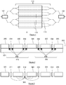
- a dual parallel I/Q (in phase/quadrature) modulator typically has the structure schematically shown in Figure 1 .
- the signal enters a splitter 101, which divides the signal into each channel of four Mach-Zehnder modulators 110, each of which comprises two waveguides 111, and an electrical RF (radio frequency) transmission line 112.
- the modulators apply the required modulation, and the signal is recombined by a combiner 102.
- the Mach-Zehnder modulator has a cross section along A as shown in Figure 2 .
- the waveguide section of the Mach-Zehnder modulator comprises a substrate 201, which contains waveguides 202.
- the RF transmission line array 203 is placed on one face of the substrate.
- Each RF transmission line comprises a signal electrode 204.
- Each signal electrode 204 has a ground electrode 205 on either side.
- the modulators may either be arranged x-cut (210), with the waveguides positioned below the gaps between the signal and ground electrodes (symmetrically around the signal electrode), or z-cut (220) with one waveguide beneath the signal electrode, and one beneath one of the ground electrodes. Normally, all modulators in an array would be the same type, but both z- and x-cut modulators are shown in Figure 2 for illustration. Intermediate ground electrodes (i.e. those between two signal electrodes) are shared between adjacent RF transmission lines.
- US 2016/033848 A1 (KATAOKA TOSHIO [JP] ET AL) 4 February 2016 (2016-02-04) discloses a prior art radiofrequency, RF, waveguide array with ground electrodes between signal electrodes.
- a first and second aspect of the invention proposes that the ground electrodes have reduced thickness (that is, height in the direction transverse to the surface of the substrate) in areas which are relatively distant from the signal electrodes. This reduces the amount of the material (typically gold) which is required to produce the ground electrodes, with acceptable (or even no) reduction in the quality of the RF transmission lines.
- Each ground electrode which typically has a substantially homogenous chemical composition, may be formed in a single process step which produces the areas of reduced thickness and areas of greater thickness closer to the signal electrodes.
- the first aspect proposes a radio frequency, RF, waveguide array.
- the array comprises a substrate and an electrical RF transmission line array.
- the substrate comprises a plurality of optical waveguides, each waveguide being elongate in a first direction.
- the electrical RF transmission line array is located on a face of the substrate and comprises a plurality of signal electrodes and a plurality of ground electrodes. Each electrode extends in the first direction.
- Each signal electrode is positioned to provide a signal to two respective waveguides.
- the ground electrodes include one intermediate ground electrode positioned between each pair of signal electrodes.
- the intermediate ground electrodes have a first height in one or more first regions and a second height in at least one second region, where the height is measured in a direction perpendicular to the face of the substrate, each intermediate ground electrode having a U-shaped cross section perpendicular to the first direction.
- each first region is closer to a respective signal electrode than the second region.
- the second height is less than 75% of the first height.
- the second aspect proposes a radio frequency, RF, waveguide array.
- the array comprises a substrate and an electrical RF transmission line array.
- the substrate comprises a plurality of optical waveguides, each waveguide being elongate in a first direction.
- the electrical RF transmission line array is located on a face of the substrate and comprises a plurality of signal electrodes and a plurality of ground electrodes. Each electrode extends in the first direction.
- Each signal electrode is positioned to provide a signal to two respective waveguides.
- the ground electrodes include two or more intermediate ground electrodes positioned between each pair of signal electrodes.
- the intermediate ground electrodes have a first height in one or more first regions and a second height in at least one second region, where the height is measured in a direction perpendicular to the face of the substrate, each intermediate ground electrode having a L-shaped cross section perpendicular to the first direction.
- each first region is closer to a respective signal electrode than the second region.
- the second height is less than 75% of the first height.
- a dual parallel in-phase/quadrature, I/Q, modulator comprising an RF waveguide array according to either the first or second aspect.
- Length is used herein to refer to distance in the direction of travel of the RF signals in the RF transmission lines - i.e. "out of the page” in Figure 2 .
- Height is used herein to refer to distance in a direction perpendicular to the face of the substrate to which the RF transmission lines are attached - i.e. vertically in Figure 2 .
- Width is used to refer to distance in a direction perpendicular to both height and length - i.e. horizontally in Figure 2 , unless otherwise specified.
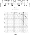
- Figure 3 shows the electric field line distribution of the RF transmission line array shown in Figure 2 (the substrate and waveguides are omitted for clarity).
- Signal electrodes are labelled 311, 312, 313, 314 from left to right
- ground electrodes are labelled 321, 322, 323, 324, 325 from left to right.
- 321 and 325 are edge ground electrodes
- 322, 323 and 324 are intermediate ground electrodes.
- the signal from the signal electrode 312 extends through the ground electrodes 322 and 323, and to the nearest other signal electrodes 311 and 313.
- the wide electrical field distribution gives rise to high frequency losses - even in the case of a single transmission line - and the spread of the field to adjacent lines causes unwanted "crosstalk", i.e. interference on one line caused by another.
- ground electrodes typically have a width above 100 microns.
- narrower ground electrodes in fact improves performance of the transmission line at high frequencies. This is unexpected, as it moves the structure of the transmission line further from the "ideal" case of a coplanar waveguide (where the ground electrodes have infinite width). It is theorised that the improvement is due to tighter confinement of the electrical field.
- each intermediate ground electrode into at least two, as shown in Figure 4 .
- each signal electrode 411, 412, 413, 414 is adjacent to two ground electrodes 421, 422, 423, ... 428.
- signal electrode 412 is adjacent to ground electrodes 423 and 424.
- Intermediate ground electrodes 422, 423, 424, 425, 426, 427 are separated by channels 431, 432, 433.
- Each of the ground electrodes has a width which is preferably less than 150 microns, and preferably less than or equal to 100 microns. This separation not only provides narrower ground electrodes, improving high frequency performance, but also provides some separation between the RF transmission lines, which reduces crosstalk.
- Figure 5 shows these improvements - Figure 5 is a graph of the deviation from the ideal case of the transmission (S 21 ) curve of on one of the lines, with the lower curve showing a prior art transmission line array, and the upper curve showing the transmission line array of Figure 4 . At higher frequencies, the transmission parameter S 21 is closer to the ideal case.
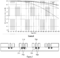
- a further advantage of the narrow ground structure is that it improves electro-optical efficiency between the transmission lines and the waveguides.
- the electric field 711, 721 from the signal electrodes 712, 722 is more focussed, more of the field passes through the waveguides 713 (shown in z-cut) and 723 (shown in x-cut).
- This benefit is maximised when the width of the ground electrodes is similar to the width of the waveguides - e.g. less than twice the width of the waveguide.
- the benefit is greatest in the z-cut configuration. In the z-cut configuration, only narrowing of the ground electrode which is above the waveguide provides any benefit to the electro-optic efficiency.
- the signal electrode, waveguide, and ground electrodes 810 not above a waveguide in the z-cut case are unchanged.
- the ground electrodes 800 which are located above a waveguide in the z-cut case, or both the ground electrodes in the x-cut case, each have a plurality of slots 801 in them. The slots are elongate along the length of the ground electrode, and divide the electrode into a region which is above the waveguide, and a region which is not.
- the region above the waveguide can be made narrow in order to provide improved electro-optic efficiency, and the region not above the waveguide and regions of the ground electrode which do not have slots act to smooth out the S 21 curve. Although only two slots are shown per ground electrode, there may be any number of slots per ground electrode, preferably all co-linear and extending in the same direction.
- the length of the slots may be selected based on a number of constraints. If the slots are too short, then they have no effect on the performance of the modulator. If the slots are too long, then they form cavities in the line which can cause notches on the S 21 curve. Possible length values are above 50 microns, and below 350 microns. At length values above 350 microns, resonances will become apparent in the S 21 curve, though for some applications these may be acceptable at higher lengths.
- the slot may have a length of 80 microns, and the distance between slots may be 40 microns, resulting in a "cell" of 120 microns which is duplicated along the line.
- the slots may be arranged periodically (that is, all the slots have the same length, and slots are spaced apart from each other pairwise by a certain fixed distance) or non-periodically. Arranging the slots periodically may cause resonances in the line, but these could be compensated for by other means.
- Figure 9A and B illustrate the low frequency behaviour of a transmission line according to Figure 4 . While the graph on Figure 5A demonstrated an case where the ground electrodes were connected with a probe station (i.e. electrically isolated from each other), Figure 9A is a graph showing the case where the ground electrodes are electrically connected at some point at or beyond the start or end of the transmission line (e.g. connected to a common ground, which will generally be the case in a packaged product as the package acts as a ground). As can be seen from the graph, there is a large amount of distortion at low frequency ranges. This is not seen in transmission line arrays without separated ground electrodes, or in single transmission lines with narrow ground electrodes, and its discovery in this case is surprising.
- the transmission line array is configured to cause increased losses to the mode compared to the architecture of Figure 4 - the higher the loss of the mode, the lower the frequency at which the mode is significant, so the waveguide can be configured to "push" the mode below the operating frequency of the waveguide.
- adjacent intermediate ground electrodes are connected in such a way that they act as a single shared electrode at low frequency, and as separated electrodes at high frequency.
- An example of the first approach is to narrow the channel between intermediate electrodes.
- the narrower the channel the higher the loss of the low frequency mode. This effect becomes significant when the channel is less than 20 microns wide, and the curve is smoother as the channel becomes narrower.
- very narrow channels can have a negative effect due to manufacturing errors causing the intermediate ground electrodes to come into contact. With current technology, this is anticipated to occur for channels less than 5 microns wide, but future improvements in manufacturing may allow for narrower channels.
- the preferred separation between ground electrodes is 10 microns.
- Another example of the first approach is to vary the width of the intermediate ground electrodes along their length. This forces changes in the distribution of the electric field in the channel, which causes the unwanted mode to become very lossy. This can be achieved by varying the width of each intermediate ground electrode independently (i.e. by varying the width of the channel, but ensuring that the intermediate ground electrodes remain separate). Alternatively, this can be done by varying the width of each intermediate ground electrode in a coordinated fashion such that adjacent intermediate ground electrodes interleave with each other.
- the channel width may be maintained constant, either as measured perpendicular to the length of the electrodes, or perpendicular to the walls of the channel.
- the minimum width of each ground electrode is preferably greater than or equal to 10 microns but less than 80 microns.
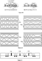
- Exemplary structures are shown in Figure 10 .
- the width variation is a "wave-like" formation over the length of the ground electrode, i.e. the width varies repeatedly between a minimum and a maximum width in a periodic or modulated periodic fashion. It will be appreciated that other variations of the width, both wave-like and not wave-like are possible.
- the structure which shows the greatest benefit is that where the channel forms a "square wave" 1001, i.e. each of the ground electrodes varies according to a square wave along its length, such that the two square waves can interleave without the ground electrodes coming into contact.
- the "square wave" pattern may be difficult to manufacture, so as an alternative the shape of the channel (and variation in width of the intermediate ground electrodes) may form a triangular wave 1002, a sinusoidal wave 1003, or other varying formation which is a function of the distance along the electrode. Where the width varies by a periodic function, the wavelength of that function may be changed over the length of the electrodes (i.e. modulated), since using a periodic function with constant wavelength may result in resonances and the formation of cavities within the waveguide. An example of this is shown for a sinusoidal wave 1004. Cavities in the waveguide may also be avoided by providing a periodic function with a low wavelength, e.g. less than 600 microns, more preferably less than 500 microns, e.g. 450 microns, more preferably less than 250 microns, e.g. 200 microns.
- a periodic function with a low wavelength, e.g. less than 600 microns, more preferably less than 500 microns, e.g.
- the width may vary between a width less than twice the width of the waveguides and a larger width, in order to provide some of the advantages of narrow waveguides mentioned above with reference to Figure 7 .
- Yet another example of the first approach is to introduce a material 1101, 1102, 1103 into the channel which causes high RF losses at the frequencies at which the unwanted mode is problematic, e.g. a material with a high absorption, and/or with a high loss tangent (e.g. greater than 0.1), for example a magnetic loaded material. Since only the unwanted mode propagates significantly into the channel, this would favourably cause losses to the unwanted modes.
- the material may completely fill the channel 1101, or it may only partially fill the channel along its height 1102, width 1103, and/or length.
- the frequencies at which the losses are required are those where a) the unwanted mode is significant (e.g. less than 10GHz, or less than 5GHz) and b) the performance of the waveguide at those frequencies is important (e.g. greater than 0.5GHz, greater than 1GHz, or otherwise according to the performance requirements of the application).
- the second approach, illustrated in Figure 12 may be achieved by connecting adjacent intermediate ground electrodes with a low pass filter 1201 (shown schematically), or some other structure which acts equivalently to a low pass filter.
- the adjacent intermediate ground electrodes may be connected by a thin (e.g. less than 1 micron) metal layer 1202 (e.g. formed directly on the substrate), which will cause the intermediate ground electrodes to be effectively connected at low frequencies, and effectively disconnected at high frequencies.
- a thin (e.g. less than 1 micron) metal layer 1202 e.g. formed directly on the substrate
- the unwanted mode which only occurs for separate ground electrodes, cannot occur at low frequencies. Since the benefits of separate ground electrodes are only significant at high frequencies (e.g. above 25GHz), there is little downside to connecting the ground electrodes at low frequency.
- a further improvement that can be made to RF transmission line arrays is to reduce the amount of gold required.
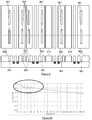
- the ground electrodes have the same height as the signal electrodes. However, the behaviour of the transmission line is mostly governed by the regions of the ground electrodes closest to the signal electrodes. As such, a ground electrode structure as shown in Figure 13 can be used to reduce the amount of gold required.
- Each ground electrode 1300 has first regions 1301 close to the respective signal electrodes which are the same height as the signal electrodes, and a second region 1302 further from the signal electrode which is a reduced height. In this way, the amount of gold needed to form the ground electrodes can be significantly reduced.
- the reduced height may be 75% of the height of the signal electrodes, or less, for example less than 50%, 25%, 10% or 5% of the height of the signal electrodes, or less than 10 microns, 5 microns, 2 microns, or 1 micron.
- the ground electrodes may have a U-shaped profile.
- Intermediate ground electrodes 1400 may be provided with a first region 1301 having the same height as a signal electrode, and a second region 1302 having a reduced height, where the first region is further from the signal electrode.
- each intermediate ground electrode may have an L-shaped profile. Reducing the height of the ground electrodes in these embodiments also helps reduce the risk of shorts in the channel - where the height of the ground electrodes adjacent to the channel is similar to or less than the width of the channel, the channel is easier to manufacture without shorts.
- the reduced height may be less than 75% of the height of the signal electrodes, more preferably less than 50%, more preferably less than 10%, more preferably less than 3%. In microns, the reduced height may be less than or equal to 5 microns, more preferably less than or equal to 3 microns, more preferably less than or equal to 1.5 microns.
- any design for a waveguide array according to the above examples will be a trade-off of various factors, and the performance required will depend on the application. Therefore, a feature being described as advantageous does not mean that that feature is required - in many applications, there will be sufficient tolerances that some crosstalk or non-smoothness in the S 21 curve is acceptable, so a less preferred example may be used.
Landscapes
- Physics & Mathematics (AREA)
- Nonlinear Science (AREA)
- General Physics & Mathematics (AREA)
- Optics & Photonics (AREA)
- Electromagnetism (AREA)
- Optical Modulation, Optical Deflection, Nonlinear Optics, Optical Demodulation, Optical Logic Elements (AREA)
Applications Claiming Priority (2)
| Application Number | Priority Date | Filing Date | Title |
|---|---|---|---|
| GBGB1611576.8A GB201611576D0 (en) | 2016-07-01 | 2016-07-01 | Ground structure in RF waveguide array |
| PCT/GB2017/051934 WO2018002656A1 (en) | 2016-07-01 | 2017-06-30 | Ground structure in rf waveguide array |
Publications (2)
| Publication Number | Publication Date |
|---|---|
| EP3479170A1 EP3479170A1 (en) | 2019-05-08 |
| EP3479170B1 true EP3479170B1 (en) | 2020-08-05 |
Family
ID=56891341
Family Applications (1)
| Application Number | Title | Priority Date | Filing Date |
|---|---|---|---|
| EP17737025.1A Active EP3479170B1 (en) | 2016-07-01 | 2017-06-30 | Ground structure in rf waveguide array |
Country Status (6)
| Country | Link |
|---|---|
| US (1) | US10678114B2 (enExample) |
| EP (1) | EP3479170B1 (enExample) |
| JP (1) | JP7242302B2 (enExample) |
| CN (1) | CN109416495B (enExample) |
| GB (1) | GB201611576D0 (enExample) |
| WO (1) | WO2018002656A1 (enExample) |
Families Citing this family (3)
| Publication number | Priority date | Publication date | Assignee | Title |
|---|---|---|---|---|
| GB201611576D0 (en) * | 2016-07-01 | 2016-08-17 | Oclaro Tech Ltd | Ground structure in RF waveguide array |
| GB201611574D0 (en) | 2016-07-01 | 2016-08-17 | Oclaro Tech Ltd | Ground structure in rf waveguide array |
| JP7056236B2 (ja) * | 2018-03-02 | 2022-04-19 | 富士通オプティカルコンポーネンツ株式会社 | 光変調器、及びこれを用いた光トランシーバモジュール |
Family Cites Families (36)
| Publication number | Priority date | Publication date | Assignee | Title |
|---|---|---|---|---|
| JPH08166566A (ja) * | 1994-12-14 | 1996-06-25 | Nippon Telegr & Teleph Corp <Ntt> | 光制御デバイス |
| JP3527410B2 (ja) * | 1998-06-15 | 2004-05-17 | 株式会社リコー | コプレーナーストリップライン |
| JP4041226B2 (ja) | 1998-09-30 | 2008-01-30 | 京セラ株式会社 | 光半導体装置 |
| US6580843B2 (en) | 2001-04-05 | 2003-06-17 | Fujitsu Limited | Optical device |
| JP3823873B2 (ja) | 2002-05-07 | 2006-09-20 | 富士通株式会社 | 半導体マッハツェンダ型光変調器 |
| JP3640390B2 (ja) | 2002-09-12 | 2005-04-20 | 住友大阪セメント株式会社 | 光変調器 |
| US6845183B2 (en) * | 2003-02-05 | 2005-01-18 | Jds Uniphase Corporation | Slotted electrode electro-optic modulator |
| US7171063B2 (en) * | 2004-12-01 | 2007-01-30 | Jds Uniphase Corporation | Controllable electro-optic device having substrate trenches between electrodes |
| JP4542422B2 (ja) | 2004-12-10 | 2010-09-15 | 富士通株式会社 | 光デバイス及び駆動電圧供給装置 |
| JP4926423B2 (ja) | 2005-07-27 | 2012-05-09 | アンリツ株式会社 | 光変調器 |
| JP4110182B2 (ja) * | 2006-09-30 | 2008-07-02 | 住友大阪セメント株式会社 | 光制御素子 |
| CN201007762Y (zh) | 2006-10-11 | 2008-01-16 | 北京世维通光通讯技术有限公司 | 用于有线电视系统的铌酸锂电光调制器 |
| US7844149B2 (en) * | 2007-01-12 | 2010-11-30 | Jds Uniphase Corporation | Humidity tolerant electro-optic device |
| JP5007629B2 (ja) | 2007-08-27 | 2012-08-22 | 住友大阪セメント株式会社 | 光導波路素子 |
| JP2009086336A (ja) * | 2007-09-28 | 2009-04-23 | Sumitomo Osaka Cement Co Ltd | 光導波路型デバイス |
| JP5113102B2 (ja) | 2008-02-01 | 2013-01-09 | アンリツ株式会社 | 光変調デバイス |
| JP2010066663A (ja) | 2008-09-12 | 2010-03-25 | Fujitsu Ltd | 光デバイスおよび光送信装置 |
| JP5326860B2 (ja) | 2009-06-25 | 2013-10-30 | 富士通オプティカルコンポーネンツ株式会社 | 光導波路デバイス |
| JP5487774B2 (ja) * | 2009-07-27 | 2014-05-07 | 富士通オプティカルコンポーネンツ株式会社 | 光デバイスおよび光送信機 |
| GB201015169D0 (en) * | 2010-09-13 | 2010-10-27 | Oclaro Technology Ltd | Electro-optic devices |
| TWI470872B (zh) * | 2010-11-29 | 2015-01-21 | Univ Chung Hua | 微帶線結構 |
| JP2011100168A (ja) | 2011-02-21 | 2011-05-19 | Sumitomo Osaka Cement Co Ltd | 光導波路素子 |
| JP5742382B2 (ja) | 2011-03-31 | 2015-07-01 | 住友大阪セメント株式会社 | 進行波型光変調素子 |
| JP5077480B2 (ja) | 2011-12-19 | 2012-11-21 | 住友大阪セメント株式会社 | 光導波路素子 |
| JP5229378B2 (ja) | 2011-12-19 | 2013-07-03 | 住友大阪セメント株式会社 | 光導波路素子 |
| JP5773440B2 (ja) | 2012-01-31 | 2015-09-02 | 住友大阪セメント株式会社 | 光変調器 |
| EP2940513A1 (en) | 2012-12-27 | 2015-11-04 | Fujikura Ltd. | Light modulation element |
| JP5711287B2 (ja) | 2013-03-26 | 2015-04-30 | 住友大阪セメント株式会社 | 光制御デバイス |
| JP5590175B1 (ja) | 2013-03-26 | 2014-09-17 | 住友大阪セメント株式会社 | 光変調器 |
| JP6317904B2 (ja) | 2013-10-02 | 2018-04-25 | 日立ジョンソンコントロールズ空調株式会社 | モータ制御装置、及び空気調和機 |
| JP5991339B2 (ja) | 2014-03-31 | 2016-09-14 | 住友大阪セメント株式会社 | 光制御素子 |
| JP6107869B2 (ja) | 2015-03-31 | 2017-04-05 | 住友大阪セメント株式会社 | 光変調器 |
| JP2016194537A (ja) * | 2015-03-31 | 2016-11-17 | 住友大阪セメント株式会社 | 導波路型光素子 |
| JP6350563B2 (ja) | 2016-02-29 | 2018-07-04 | 住友大阪セメント株式会社 | 光変調器、及び光変調器を用いた光送信装置 |
| GB201611576D0 (en) * | 2016-07-01 | 2016-08-17 | Oclaro Tech Ltd | Ground structure in RF waveguide array |
| GB201611574D0 (en) * | 2016-07-01 | 2016-08-17 | Oclaro Tech Ltd | Ground structure in rf waveguide array |
-
2016
- 2016-07-01 GB GBGB1611576.8A patent/GB201611576D0/en not_active Ceased
-
2017
- 2017-06-30 CN CN201780040267.5A patent/CN109416495B/zh active Active
- 2017-06-30 WO PCT/GB2017/051934 patent/WO2018002656A1/en not_active Ceased
- 2017-06-30 US US16/307,231 patent/US10678114B2/en active Active
- 2017-06-30 EP EP17737025.1A patent/EP3479170B1/en active Active
- 2017-06-30 JP JP2018567823A patent/JP7242302B2/ja active Active
Non-Patent Citations (1)
| Title |
|---|
| None * |
Also Published As
| Publication number | Publication date |
|---|---|
| WO2018002656A1 (en) | 2018-01-04 |
| US10678114B2 (en) | 2020-06-09 |
| EP3479170A1 (en) | 2019-05-08 |
| GB201611576D0 (en) | 2016-08-17 |
| JP2019525226A (ja) | 2019-09-05 |
| CN109416495B (zh) | 2022-07-05 |
| CN109416495A (zh) | 2019-03-01 |
| US20190196295A1 (en) | 2019-06-27 |
| JP7242302B2 (ja) | 2023-03-20 |
Similar Documents
| Publication | Publication Date | Title |
|---|---|---|
| EP3479169B1 (en) | Ground structure in rf waveguide array | |
| EP3479170B1 (en) | Ground structure in rf waveguide array | |
| US10027088B2 (en) | Integrated semiconductor optical element and manufacturing method for same | |
| EP3913425B1 (en) | Semiconductor mach zehnder optical modulator | |
| WO2009090687A1 (ja) | 光変調器 | |
| JP6348880B2 (ja) | 半導体マッハツェンダ光変調器 | |
| JP5917645B2 (ja) | 光スイッチ素子 | |
| JP2019045666A (ja) | 半導体マッハツェンダ光変調器およびiq変調器 | |
| JP5935934B1 (ja) | 光変調器及びそれを用いた光送信装置 | |
| EP3926393B1 (en) | Semiconductor mach-zehnder optical modulator and iq modulator | |
| US11016360B1 (en) | Optical modulator RF electrodes | |
| TW201707272A (zh) | 高頻線路 | |
| JP5075055B2 (ja) | 光変調器 | |
| US12181770B2 (en) | Multiple air bridge electro-optic modulator | |
| TWI708984B (zh) | 半導體馬赫曾德爾光調變器及iq調變器 | |
| JP5124382B2 (ja) | 光変調器 | |
| WO2019176665A1 (ja) | 光変調器 | |
| JP5308552B2 (ja) | 光変調器 | |
| JP3303653B2 (ja) | 半導体レーザ装置、その駆動方法及びそれを用いた光通信システム | |
| JP2008134306A (ja) | 光変調器 |
Legal Events
| Date | Code | Title | Description |
|---|---|---|---|
| STAA | Information on the status of an ep patent application or granted ep patent |
Free format text: STATUS: UNKNOWN |
|
| STAA | Information on the status of an ep patent application or granted ep patent |
Free format text: STATUS: THE INTERNATIONAL PUBLICATION HAS BEEN MADE |
|
| PUAI | Public reference made under article 153(3) epc to a published international application that has entered the european phase |
Free format text: ORIGINAL CODE: 0009012 |
|
| STAA | Information on the status of an ep patent application or granted ep patent |
Free format text: STATUS: REQUEST FOR EXAMINATION WAS MADE |
|
| 17P | Request for examination filed |
Effective date: 20181130 |
|
| AK | Designated contracting states |
Kind code of ref document: A1 Designated state(s): AL AT BE BG CH CY CZ DE DK EE ES FI FR GB GR HR HU IE IS IT LI LT LU LV MC MK MT NL NO PL PT RO RS SE SI SK SM TR |
|
| AX | Request for extension of the european patent |
Extension state: BA ME |
|
| RAP1 | Party data changed (applicant data changed or rights of an application transferred) |
Owner name: LUMENTUM TECHNOLOGY UK LIMITED |
|
| DAV | Request for validation of the european patent (deleted) | ||
| DAX | Request for extension of the european patent (deleted) | ||
| GRAP | Despatch of communication of intention to grant a patent |
Free format text: ORIGINAL CODE: EPIDOSNIGR1 |
|
| STAA | Information on the status of an ep patent application or granted ep patent |
Free format text: STATUS: GRANT OF PATENT IS INTENDED |
|
| INTG | Intention to grant announced |
Effective date: 20200203 |
|
| GRAS | Grant fee paid |
Free format text: ORIGINAL CODE: EPIDOSNIGR3 |
|
| GRAA | (expected) grant |
Free format text: ORIGINAL CODE: 0009210 |
|
| STAA | Information on the status of an ep patent application or granted ep patent |
Free format text: STATUS: THE PATENT HAS BEEN GRANTED |
|
| AK | Designated contracting states |
Kind code of ref document: B1 Designated state(s): AL AT BE BG CH CY CZ DE DK EE ES FI FR GB GR HR HU IE IS IT LI LT LU LV MC MK MT NL NO PL PT RO RS SE SI SK SM TR |
|
| REG | Reference to a national code |
Ref country code: GB Ref legal event code: FG4D |
|
| REG | Reference to a national code |
Ref country code: CH Ref legal event code: EP |
|
| REG | Reference to a national code |
Ref country code: AT Ref legal event code: REF Ref document number: 1299549 Country of ref document: AT Kind code of ref document: T Effective date: 20200815 |
|
| REG | Reference to a national code |
Ref country code: DE Ref legal event code: R096 Ref document number: 602017021121 Country of ref document: DE |
|
| REG | Reference to a national code |
Ref country code: IE Ref legal event code: FG4D |
|
| REG | Reference to a national code |
Ref country code: DE Ref legal event code: R081 Ref document number: 602017021121 Country of ref document: DE Owner name: LUMENTUM TECHNOLOGY UK LIMITED, TOWCESTER, GB Free format text: FORMER OWNER: LUMENTUM TECHNOLOGY UK LTD., TOWCESTER, NORTHAMPTONSHIRE, GB |
|
| REG | Reference to a national code |
Ref country code: LT Ref legal event code: MG4D |
|
| REG | Reference to a national code |
Ref country code: NL Ref legal event code: MP Effective date: 20200805 |
|
| REG | Reference to a national code |
Ref country code: AT Ref legal event code: MK05 Ref document number: 1299549 Country of ref document: AT Kind code of ref document: T Effective date: 20200805 |
|
| PG25 | Lapsed in a contracting state [announced via postgrant information from national office to epo] |
Ref country code: FI Free format text: LAPSE BECAUSE OF FAILURE TO SUBMIT A TRANSLATION OF THE DESCRIPTION OR TO PAY THE FEE WITHIN THE PRESCRIBED TIME-LIMIT Effective date: 20200805 Ref country code: LT Free format text: LAPSE BECAUSE OF FAILURE TO SUBMIT A TRANSLATION OF THE DESCRIPTION OR TO PAY THE FEE WITHIN THE PRESCRIBED TIME-LIMIT Effective date: 20200805 Ref country code: BG Free format text: LAPSE BECAUSE OF FAILURE TO SUBMIT A TRANSLATION OF THE DESCRIPTION OR TO PAY THE FEE WITHIN THE PRESCRIBED TIME-LIMIT Effective date: 20201105 Ref country code: AT Free format text: LAPSE BECAUSE OF FAILURE TO SUBMIT A TRANSLATION OF THE DESCRIPTION OR TO PAY THE FEE WITHIN THE PRESCRIBED TIME-LIMIT Effective date: 20200805 Ref country code: PT Free format text: LAPSE BECAUSE OF FAILURE TO SUBMIT A TRANSLATION OF THE DESCRIPTION OR TO PAY THE FEE WITHIN THE PRESCRIBED TIME-LIMIT Effective date: 20201207 Ref country code: ES Free format text: LAPSE BECAUSE OF FAILURE TO SUBMIT A TRANSLATION OF THE DESCRIPTION OR TO PAY THE FEE WITHIN THE PRESCRIBED TIME-LIMIT Effective date: 20200805 Ref country code: NO Free format text: LAPSE BECAUSE OF FAILURE TO SUBMIT A TRANSLATION OF THE DESCRIPTION OR TO PAY THE FEE WITHIN THE PRESCRIBED TIME-LIMIT Effective date: 20201105 Ref country code: GR Free format text: LAPSE BECAUSE OF FAILURE TO SUBMIT A TRANSLATION OF THE DESCRIPTION OR TO PAY THE FEE WITHIN THE PRESCRIBED TIME-LIMIT Effective date: 20201106 Ref country code: SE Free format text: LAPSE BECAUSE OF FAILURE TO SUBMIT A TRANSLATION OF THE DESCRIPTION OR TO PAY THE FEE WITHIN THE PRESCRIBED TIME-LIMIT Effective date: 20200805 Ref country code: HR Free format text: LAPSE BECAUSE OF FAILURE TO SUBMIT A TRANSLATION OF THE DESCRIPTION OR TO PAY THE FEE WITHIN THE PRESCRIBED TIME-LIMIT Effective date: 20200805 |
|
| PG25 | Lapsed in a contracting state [announced via postgrant information from national office to epo] |
Ref country code: PL Free format text: LAPSE BECAUSE OF FAILURE TO SUBMIT A TRANSLATION OF THE DESCRIPTION OR TO PAY THE FEE WITHIN THE PRESCRIBED TIME-LIMIT Effective date: 20200805 Ref country code: RS Free format text: LAPSE BECAUSE OF FAILURE TO SUBMIT A TRANSLATION OF THE DESCRIPTION OR TO PAY THE FEE WITHIN THE PRESCRIBED TIME-LIMIT Effective date: 20200805 Ref country code: LV Free format text: LAPSE BECAUSE OF FAILURE TO SUBMIT A TRANSLATION OF THE DESCRIPTION OR TO PAY THE FEE WITHIN THE PRESCRIBED TIME-LIMIT Effective date: 20200805 Ref country code: NL Free format text: LAPSE BECAUSE OF FAILURE TO SUBMIT A TRANSLATION OF THE DESCRIPTION OR TO PAY THE FEE WITHIN THE PRESCRIBED TIME-LIMIT Effective date: 20200805 Ref country code: IS Free format text: LAPSE BECAUSE OF FAILURE TO SUBMIT A TRANSLATION OF THE DESCRIPTION OR TO PAY THE FEE WITHIN THE PRESCRIBED TIME-LIMIT Effective date: 20201205 |
|
| PG25 | Lapsed in a contracting state [announced via postgrant information from national office to epo] |
Ref country code: EE Free format text: LAPSE BECAUSE OF FAILURE TO SUBMIT A TRANSLATION OF THE DESCRIPTION OR TO PAY THE FEE WITHIN THE PRESCRIBED TIME-LIMIT Effective date: 20200805 Ref country code: SM Free format text: LAPSE BECAUSE OF FAILURE TO SUBMIT A TRANSLATION OF THE DESCRIPTION OR TO PAY THE FEE WITHIN THE PRESCRIBED TIME-LIMIT Effective date: 20200805 Ref country code: DK Free format text: LAPSE BECAUSE OF FAILURE TO SUBMIT A TRANSLATION OF THE DESCRIPTION OR TO PAY THE FEE WITHIN THE PRESCRIBED TIME-LIMIT Effective date: 20200805 Ref country code: CZ Free format text: LAPSE BECAUSE OF FAILURE TO SUBMIT A TRANSLATION OF THE DESCRIPTION OR TO PAY THE FEE WITHIN THE PRESCRIBED TIME-LIMIT Effective date: 20200805 Ref country code: RO Free format text: LAPSE BECAUSE OF FAILURE TO SUBMIT A TRANSLATION OF THE DESCRIPTION OR TO PAY THE FEE WITHIN THE PRESCRIBED TIME-LIMIT Effective date: 20200805 |
|
| REG | Reference to a national code |
Ref country code: DE Ref legal event code: R097 Ref document number: 602017021121 Country of ref document: DE |
|
| PG25 | Lapsed in a contracting state [announced via postgrant information from national office to epo] |
Ref country code: AL Free format text: LAPSE BECAUSE OF FAILURE TO SUBMIT A TRANSLATION OF THE DESCRIPTION OR TO PAY THE FEE WITHIN THE PRESCRIBED TIME-LIMIT Effective date: 20200805 |
|
| PLBE | No opposition filed within time limit |
Free format text: ORIGINAL CODE: 0009261 |
|
| STAA | Information on the status of an ep patent application or granted ep patent |
Free format text: STATUS: NO OPPOSITION FILED WITHIN TIME LIMIT |
|
| PG25 | Lapsed in a contracting state [announced via postgrant information from national office to epo] |
Ref country code: SK Free format text: LAPSE BECAUSE OF FAILURE TO SUBMIT A TRANSLATION OF THE DESCRIPTION OR TO PAY THE FEE WITHIN THE PRESCRIBED TIME-LIMIT Effective date: 20200805 |
|
| 26N | No opposition filed |
Effective date: 20210507 |
|
| PG25 | Lapsed in a contracting state [announced via postgrant information from national office to epo] |
Ref country code: IT Free format text: LAPSE BECAUSE OF FAILURE TO SUBMIT A TRANSLATION OF THE DESCRIPTION OR TO PAY THE FEE WITHIN THE PRESCRIBED TIME-LIMIT Effective date: 20200805 |
|
| PG25 | Lapsed in a contracting state [announced via postgrant information from national office to epo] |
Ref country code: SI Free format text: LAPSE BECAUSE OF FAILURE TO SUBMIT A TRANSLATION OF THE DESCRIPTION OR TO PAY THE FEE WITHIN THE PRESCRIBED TIME-LIMIT Effective date: 20200805 |
|
| PG25 | Lapsed in a contracting state [announced via postgrant information from national office to epo] |
Ref country code: MC Free format text: LAPSE BECAUSE OF FAILURE TO SUBMIT A TRANSLATION OF THE DESCRIPTION OR TO PAY THE FEE WITHIN THE PRESCRIBED TIME-LIMIT Effective date: 20200805 |
|
| REG | Reference to a national code |
Ref country code: CH Ref legal event code: PL |
|
| GBPC | Gb: european patent ceased through non-payment of renewal fee |
Effective date: 20210630 |
|
| REG | Reference to a national code |
Ref country code: BE Ref legal event code: MM Effective date: 20210630 |
|
| PG25 | Lapsed in a contracting state [announced via postgrant information from national office to epo] |
Ref country code: LU Free format text: LAPSE BECAUSE OF NON-PAYMENT OF DUE FEES Effective date: 20210630 |
|
| PG25 | Lapsed in a contracting state [announced via postgrant information from national office to epo] |
Ref country code: LI Free format text: LAPSE BECAUSE OF NON-PAYMENT OF DUE FEES Effective date: 20210630 Ref country code: IE Free format text: LAPSE BECAUSE OF NON-PAYMENT OF DUE FEES Effective date: 20210630 Ref country code: GB Free format text: LAPSE BECAUSE OF NON-PAYMENT OF DUE FEES Effective date: 20210630 Ref country code: CH Free format text: LAPSE BECAUSE OF NON-PAYMENT OF DUE FEES Effective date: 20210630 |
|
| PG25 | Lapsed in a contracting state [announced via postgrant information from national office to epo] |
Ref country code: FR Free format text: LAPSE BECAUSE OF NON-PAYMENT OF DUE FEES Effective date: 20210630 |
|
| PG25 | Lapsed in a contracting state [announced via postgrant information from national office to epo] |
Ref country code: BE Free format text: LAPSE BECAUSE OF NON-PAYMENT OF DUE FEES Effective date: 20210630 |
|
| PG25 | Lapsed in a contracting state [announced via postgrant information from national office to epo] |
Ref country code: CY Free format text: LAPSE BECAUSE OF FAILURE TO SUBMIT A TRANSLATION OF THE DESCRIPTION OR TO PAY THE FEE WITHIN THE PRESCRIBED TIME-LIMIT Effective date: 20200805 |
|
| PG25 | Lapsed in a contracting state [announced via postgrant information from national office to epo] |
Ref country code: HU Free format text: LAPSE BECAUSE OF FAILURE TO SUBMIT A TRANSLATION OF THE DESCRIPTION OR TO PAY THE FEE WITHIN THE PRESCRIBED TIME-LIMIT; INVALID AB INITIO Effective date: 20170630 |
|
| PG25 | Lapsed in a contracting state [announced via postgrant information from national office to epo] |
Ref country code: MK Free format text: LAPSE BECAUSE OF FAILURE TO SUBMIT A TRANSLATION OF THE DESCRIPTION OR TO PAY THE FEE WITHIN THE PRESCRIBED TIME-LIMIT Effective date: 20200805 |
|
| PG25 | Lapsed in a contracting state [announced via postgrant information from national office to epo] |
Ref country code: MT Free format text: LAPSE BECAUSE OF FAILURE TO SUBMIT A TRANSLATION OF THE DESCRIPTION OR TO PAY THE FEE WITHIN THE PRESCRIBED TIME-LIMIT Effective date: 20200805 |
|
| PGFP | Annual fee paid to national office [announced via postgrant information from national office to epo] |
Ref country code: DE Payment date: 20250630 Year of fee payment: 9 |