EP3461873B1 - Light-emitting device - Google Patents
Light-emitting device Download PDFInfo
- Publication number
- EP3461873B1 EP3461873B1 EP18196805.8A EP18196805A EP3461873B1 EP 3461873 B1 EP3461873 B1 EP 3461873B1 EP 18196805 A EP18196805 A EP 18196805A EP 3461873 B1 EP3461873 B1 EP 3461873B1
- Authority
- EP
- European Patent Office
- Prior art keywords
- light
- emitting device
- fluorescent material
- color temperature
- mass
- Prior art date
- Legal status (The legal status is an assumption and is not a legal conclusion. Google has not performed a legal analysis and makes no representation as to the accuracy of the status listed.)
- Active
Links
Images

Classifications
-
- H—ELECTRICITY
- H10—SEMICONDUCTOR DEVICES; ELECTRIC SOLID-STATE DEVICES NOT OTHERWISE PROVIDED FOR
- H10H—INORGANIC LIGHT-EMITTING SEMICONDUCTOR DEVICES HAVING POTENTIAL BARRIERS
- H10H20/00—Individual inorganic light-emitting semiconductor devices having potential barriers, e.g. light-emitting diodes [LED]
- H10H20/80—Constructional details
- H10H20/85—Packages
- H10H20/851—Wavelength conversion means
- H10H20/8511—Wavelength conversion means characterised by their material, e.g. binder
- H10H20/8512—Wavelength conversion materials
- H10H20/8513—Wavelength conversion materials having two or more wavelength conversion materials
-
- C—CHEMISTRY; METALLURGY
- C09—DYES; PAINTS; POLISHES; NATURAL RESINS; ADHESIVES; COMPOSITIONS NOT OTHERWISE PROVIDED FOR; APPLICATIONS OF MATERIALS NOT OTHERWISE PROVIDED FOR
- C09K—MATERIALS FOR MISCELLANEOUS APPLICATIONS, NOT PROVIDED FOR ELSEWHERE
- C09K11/00—Luminescent materials, e.g. electroluminescent or chemiluminescent
- C09K11/08—Luminescent materials, e.g. electroluminescent or chemiluminescent containing inorganic luminescent materials
- C09K11/77—Luminescent materials, e.g. electroluminescent or chemiluminescent containing inorganic luminescent materials containing rare earth metals
- C09K11/7728—Luminescent materials, e.g. electroluminescent or chemiluminescent containing inorganic luminescent materials containing rare earth metals containing europium
- C09K11/7734—Aluminates
-
- C—CHEMISTRY; METALLURGY
- C09—DYES; PAINTS; POLISHES; NATURAL RESINS; ADHESIVES; COMPOSITIONS NOT OTHERWISE PROVIDED FOR; APPLICATIONS OF MATERIALS NOT OTHERWISE PROVIDED FOR
- C09K—MATERIALS FOR MISCELLANEOUS APPLICATIONS, NOT PROVIDED FOR ELSEWHERE
- C09K11/00—Luminescent materials, e.g. electroluminescent or chemiluminescent
- C09K11/08—Luminescent materials, e.g. electroluminescent or chemiluminescent containing inorganic luminescent materials
- C09K11/77—Luminescent materials, e.g. electroluminescent or chemiluminescent containing inorganic luminescent materials containing rare earth metals
- C09K11/7728—Luminescent materials, e.g. electroluminescent or chemiluminescent containing inorganic luminescent materials containing rare earth metals containing europium
- C09K11/77342—Silicates
-
- C—CHEMISTRY; METALLURGY
- C09—DYES; PAINTS; POLISHES; NATURAL RESINS; ADHESIVES; COMPOSITIONS NOT OTHERWISE PROVIDED FOR; APPLICATIONS OF MATERIALS NOT OTHERWISE PROVIDED FOR
- C09K—MATERIALS FOR MISCELLANEOUS APPLICATIONS, NOT PROVIDED FOR ELSEWHERE
- C09K11/00—Luminescent materials, e.g. electroluminescent or chemiluminescent
- C09K11/08—Luminescent materials, e.g. electroluminescent or chemiluminescent containing inorganic luminescent materials
- C09K11/77—Luminescent materials, e.g. electroluminescent or chemiluminescent containing inorganic luminescent materials containing rare earth metals
- C09K11/7728—Luminescent materials, e.g. electroluminescent or chemiluminescent containing inorganic luminescent materials containing rare earth metals containing europium
- C09K11/77348—Silicon Aluminium Nitrides or Silicon Aluminium Oxynitrides
-
- C—CHEMISTRY; METALLURGY
- C09—DYES; PAINTS; POLISHES; NATURAL RESINS; ADHESIVES; COMPOSITIONS NOT OTHERWISE PROVIDED FOR; APPLICATIONS OF MATERIALS NOT OTHERWISE PROVIDED FOR
- C09K—MATERIALS FOR MISCELLANEOUS APPLICATIONS, NOT PROVIDED FOR ELSEWHERE
- C09K11/00—Luminescent materials, e.g. electroluminescent or chemiluminescent
- C09K11/08—Luminescent materials, e.g. electroluminescent or chemiluminescent containing inorganic luminescent materials
- C09K11/77—Luminescent materials, e.g. electroluminescent or chemiluminescent containing inorganic luminescent materials containing rare earth metals
- C09K11/7766—Luminescent materials, e.g. electroluminescent or chemiluminescent containing inorganic luminescent materials containing rare earth metals containing two or more rare earth metals
- C09K11/7774—Aluminates
-
- H—ELECTRICITY
- H10—SEMICONDUCTOR DEVICES; ELECTRIC SOLID-STATE DEVICES NOT OTHERWISE PROVIDED FOR
- H10H—INORGANIC LIGHT-EMITTING SEMICONDUCTOR DEVICES HAVING POTENTIAL BARRIERS
- H10H20/00—Individual inorganic light-emitting semiconductor devices having potential barriers, e.g. light-emitting diodes [LED]
- H10H20/80—Constructional details
- H10H20/81—Bodies
- H10H20/822—Materials of the light-emitting regions
- H10H20/824—Materials of the light-emitting regions comprising only Group III-V materials, e.g. GaP
- H10H20/825—Materials of the light-emitting regions comprising only Group III-V materials, e.g. GaP containing nitrogen, e.g. GaN
-
- H—ELECTRICITY
- H10—SEMICONDUCTOR DEVICES; ELECTRIC SOLID-STATE DEVICES NOT OTHERWISE PROVIDED FOR
- H10H—INORGANIC LIGHT-EMITTING SEMICONDUCTOR DEVICES HAVING POTENTIAL BARRIERS
- H10H20/00—Individual inorganic light-emitting semiconductor devices having potential barriers, e.g. light-emitting diodes [LED]
- H10H20/80—Constructional details
- H10H20/85—Packages
- H10H20/8506—Containers
-
- H—ELECTRICITY
- H10—SEMICONDUCTOR DEVICES; ELECTRIC SOLID-STATE DEVICES NOT OTHERWISE PROVIDED FOR
- H10H—INORGANIC LIGHT-EMITTING SEMICONDUCTOR DEVICES HAVING POTENTIAL BARRIERS
- H10H20/00—Individual inorganic light-emitting semiconductor devices having potential barriers, e.g. light-emitting diodes [LED]
- H10H20/80—Constructional details
- H10H20/85—Packages
- H10H20/851—Wavelength conversion means
- H10H20/8511—Wavelength conversion means characterised by their material, e.g. binder
-
- H—ELECTRICITY
- H10—SEMICONDUCTOR DEVICES; ELECTRIC SOLID-STATE DEVICES NOT OTHERWISE PROVIDED FOR
- H10H—INORGANIC LIGHT-EMITTING SEMICONDUCTOR DEVICES HAVING POTENTIAL BARRIERS
- H10H20/00—Individual inorganic light-emitting semiconductor devices having potential barriers, e.g. light-emitting diodes [LED]
- H10H20/80—Constructional details
- H10H20/85—Packages
- H10H20/851—Wavelength conversion means
- H10H20/8515—Wavelength conversion means not being in contact with the bodies
-
- H—ELECTRICITY
- H10—SEMICONDUCTOR DEVICES; ELECTRIC SOLID-STATE DEVICES NOT OTHERWISE PROVIDED FOR
- H10H—INORGANIC LIGHT-EMITTING SEMICONDUCTOR DEVICES HAVING POTENTIAL BARRIERS
- H10H20/00—Individual inorganic light-emitting semiconductor devices having potential barriers, e.g. light-emitting diodes [LED]
- H10H20/80—Constructional details
- H10H20/85—Packages
- H10H20/852—Encapsulations
- H10H20/854—Encapsulations characterised by their material, e.g. epoxy or silicone resins
-
- H—ELECTRICITY
- H10—SEMICONDUCTOR DEVICES; ELECTRIC SOLID-STATE DEVICES NOT OTHERWISE PROVIDED FOR
- H10H—INORGANIC LIGHT-EMITTING SEMICONDUCTOR DEVICES HAVING POTENTIAL BARRIERS
- H10H20/00—Individual inorganic light-emitting semiconductor devices having potential barriers, e.g. light-emitting diodes [LED]
- H10H20/80—Constructional details
- H10H20/85—Packages
- H10H20/857—Interconnections, e.g. lead-frames, bond wires or solder balls
Definitions
- the present disclosure relates to a light-emitting device.
- a light-emitting device as defined in independent claim 1 is provided.
- a lighting tool including the light-emitting device is also provided.
- the light-emitting device includes a light-emitting element having a peak light-emitting wavelength in the range of 440 nm to 470 nm, and a fluorescent member.
- the fluorescent member includes a first fluorescent material, a second fluorescent material and a third fluorescent material.
- the light-emitting device has an emission spectrum with the ratio of the effective radiant intensity for melatonin secretion suppression to the effective radiant intensity for blue-light retinal damage (hereinafter simply referred to as "effective radiant intensity ratio") in the specific range determined by the correlated color temperature of light emitted by the light-emitting device. This further reduces the effects of light emitted by the light-emitting device on the human body compared with known light-emitting devices while reducing a decrease in the luminous flux of the light-emitting device.
- the effects on the human body as used herein refer to the risk of blue-light retinal damage and inhibition of melatonin secretion suppression.
- an effective radiant intensity L B is obtained by integrating the product of an action function B ( ⁇ ) of blue-light retinal damage or melatonin secretion suppression and the spectral distribution (spectral radiance) L ( ⁇ ) of a light-emitting device in a predetermined wavelength range.
- an action function B ( ⁇ ) of blue-light retinal damage or melatonin secretion suppression and the spectral distribution (spectral radiance) L ( ⁇ ) of a light-emitting device in a predetermined wavelength range.
- the luminosity of the subject light-emitting device is equalized to the luminosity of a light-emitting device to be compared.
- the luminous flux of the subject light-emitting device is measured using an integrating sphere to obtain a coefficient that equalizes the luminous flux of the subject light-emitting device to the luminous flux of the light-emitting device to be compared.
- the spectrum of the subject light-emitting device is then multiplied by the coefficient to obtain a spectral distribution to be used for the calculation of the effective radiant intensity for the relative comparison.
- An action function of blue-light retinal damage is defined, for example, by JIS C 7550:2014.
- an action function of melatonin secretion suppression is defined, for example, in G. C.
- the light-emitting device with a correlated color temperature of 2700 K to less than 3500 K has an effective radiant intensity ratio of 1.53 to 1.70, preferably 1.54 to 1.65, and more preferably 1.54 to 1.63 to achieve a balance between luminosity and the effects on the human body.
- the light-emitting device with a correlated color temperature of 3500 K to less than 4500 K has an effective radiant intensity ratio of 1.40 to 1.70, preferably 1.45 to 1.70, and more preferably 1.46 to 1.68.
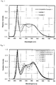
- the light-emitting device 100 is a surface-mount light-emitting device.
- the light-emitting device 100 includes a light-emitting element 10, and a molded body 40 in which the light-emitting element 10 is disposed.
- the light-emitting element 10 emits visible light at short wavelengths (e.g., in the range of 380 nm to 485 nm) and has a peak light emission wavelength in the range of 440 nm to 470 nm.
- the molded body 40 includes a first lead 20, a second lead 30, and a resin portion 42, which are formed in an integral manner.
- the molded body 40 has a recess defined by a bottom surface and side surfaces, and the light-emitting element 10 is disposed on the bottom surface of the recess.
- the light-emitting element 10 has a pair of electrodes, positive and negative, and the positive and negative electrodes are electrically connected to the first lead 20 and the second lead 30, respectively, with a wire 60.
- the light-emitting element 10 is covered with a fluorescence member 50.
- the fluorescence member 50 contains, for example, at least three fluorescent materials: a first fluorescent material 71, a second fluorescent material 72, and a third fluoride fluorescent material 73 as a fluorescent material 70, and a resin.
- the fluorescence member 50 serves not only as a member for converting the wavelength of light emitted by the light-emitting element 10, but also as a member for protecting the light-emitting element 10 from the external environment.
- the particles of the fluorescent material 70 are unevenly dispersed in the fluorescence member 50.
- the particles of the fluorescent material 70 arranged near the light-emitting element 10 in this manner efficiently converts the wavelength of light from the light-emitting element 10. This produces a light-emitting device with a high light emitting efficiency.
- the fluorescent material 70 in Fig. 2 is a mixture of the first fluorescent material 71, the second fluorescent material 72, and the third fluorescent material 73.
- the second fluorescent material may be arranged on the third fluorescent material 73
- the first fluorescent material 71 may be arranged on the second fluorescent material 72 (the arrangement not shown), or the first fluorescent material 71 may be arranged on a mixture of the second material 72 and the third fluorescent material 73 (the arrangement not shown).
- the first fluorescent material 71, the second fluorescent material 72, and the third fluorescent material 71 may be arranged in any manner.
- a semiconductor light-emitting element containing a nitride semiconductor (In X Al Y Ga 1-X-Y N where X and Y satisfy 0 ⁇ X, 0 ⁇ Y, and x + y ⁇ 1) may be used as the light source to produce a highly efficient light-emitting device that has high output linearity to the input and is resistant and stable to mechanical impact.
- the fluorescent member 50 includes at least one first fluorescent material 71 having a peak light-emitting wavelength in the range of 480 nm to less than 520 nm, at least one second fluorescent material 72 having a peak light-emitting wavelength in the range of 520 nm to less than 600 nm, and at least one third fluorescent material 73 having a peak light-emitting wavelength in the range of 600 nm to 670 nm when excited by light emitted by the light-emitting element 10.
- the fluorescent member 50 may further include other fluorescent materials and resin as appropriate.
- the first fluorescent material 71 has a peak light-emitting wavelength in the range of 480 nm to less than 520 nm, and preferably in the range of 485 nm to 515 nm.
- the first fluorescent material 71 has an emission spectrum with a half bandwidth of 30 nm or more, preferably 40 nm or more, and more preferably 50 nm or more, and, for example, 80 nm or less, and preferably 70 nm or less.
- the relative reflectance of the first fluorescent material 71 is determined as a spectral reflectance of the first fluorescent material 71 when the spectral reflectance of calcium hydrogen phosphate (CaHPO 4 with an average particle diameter of 2.7 ⁇ m) in the wavelength range of 380 nm to 435 nm is taken as 100%.
- a relative reflectance of 30% or less means that the maximum value of the relative reflectance in the range of 380 nm to 435 nm is 30% or less.
- Sr may be partially substituted by at least one element selected from the group consisting of Mg, Ca, Ba, and Zn.
- composition represented by formula (1A) may be represented by formula (1a) below: (Sr 1-x ,Eu x ) 4 Al 14 O 25 (1a)
- x satisfies 0.01 ⁇ x ⁇ 0.5, preferably satisfies 0.05 ⁇ x ⁇ 0.4, and more preferably satisfies 0.1 ⁇ x ⁇ 0.3; and Sr may be partially substituted by at least one element selected from the group consisting of Mg, Ca, Ba, and Zn.
- the first fluorescent material 71 may have an average particle diameter of, for example, 3 ⁇ m to 40 ⁇ m, and preferably 5 ⁇ m to 30 ⁇ m.
- An average particle diameter not less than the lower limit may achieve a high emission intensity.
- An average particle diameter not more than the upper limit may improve workability during the production process of the light-emitting device.
- the first fluorescent material 71 may include a surface-treated fluorescent material.
- the surface-treated fluorescent material includes, for example, fluorescent material particles containing alkaline-earth metal aluminate, and a phosphoric acid compound arranged on the surfaces of the fluorescent material particles.
- the surface-treated fluorescent material particles on the surfaces of which a phosphoric acid compound is arranged may have, for example, an improved moisture resistance.
- Examples of the phosphoric acid compound include Group 2 element (alkaline-earth metal) phosphates such as magnesium phosphate, calcium phosphate, strontium phosphate, and barium phosphate; rare-earth phosphates such as scandium phosphate, yttrium phosphate, and lanthanoid (La, Ce, Pr, Nd, Pm, Sm, Eu, Gd, Tb, Dy, Ho, Er, Tm, Yb, and Lu) phosphates; Group 13 element phosphates such as boron phosphate, aluminium phosphate, gallium phosphate, and indium phosphate; zinc phosphate, antimony phosphate, and bismuth phosphate.
- Group 2 element (alkaline-earth metal) phosphates such as magnesium phosphate, calcium phosphate, strontium phosphate, and barium phosphate
- rare-earth phosphates such as scandium phosphate, yttrium phosphate, and lant
- Preferable is at least one selected from the group consisting of these compounds, more preferable is at least one selected from the group consisting of Group 2 element phosphates, rare-earth phosphates, and Group 13 element phosphates. Still more preferable is at least one selected from the group consisting of magnesium phosphate, calcium phosphate, strontium phosphate, barium phosphate, aluminium phosphate, gallium phosphate, scandium phosphate, yttrium phosphate, and lanthanide phosphates including lanthanum phosphate.
- Particularly preferable is at least one selected from the group consisting of magnesium phosphate, calcium phosphate, strontium phosphate, barium phosphate, yttrium phosphate, and lanthanoid phosphate including lanthanum phosphate.
- the surface-treated fluorescent material may contain the phosphoric acid compound as, for example, a phosphoric acid content of, 0.0001% by mass to 20% by mass, preferably 0.1% by mass to 10% by mass, more preferably 1% by mass to 8% by mass, and still more preferably 1.5% by mass to 5.6% by mass relative to the total mass of the fluorescent material.
- the fluorescent material containing the phosphoric acid compound not less than the lower limit may have further improved moisture resistance.
- the fluorescent material containing the phosphoric acid compound not more than the upper limit can effectively reduce a decrease in emission efficiency.
- the phosphoric acid compound may have a metal content of 0.0001% by mass to 20% by mass, preferably 0.01% by mass to 10% by mass, more preferably 0.2% by mass to 3% by mass, and still more preferably 0.36% by mass to 1.4% by mass.
- the phosphoric acid compound containing the metal content in this range is likely to have a crystal structure and a composition that are more effective in achieving the object of the present disclosure.
- the surface-treated fluorescent material may have an endotherm determined by differential scanning calorimetry (DSC) at 25 °C to 650 °C of, for example, 50 J/g or less, preferably 20 J/g or less, more preferably 15 J/g or less, and still more preferably substantially 0 J/g.
- the endotherm being substantially 0 J/g as used herein means that no endothermic peak was observed in DSC.
- Such a fluorescent material is obtained by, for example, heat-treating the phosphoric acid compound-adhered fluorescent material particles at a specific temperature. Heat-treating the adhered phosphoric acid compound at a specific temperature causes physical or chemical change, and the resultant fluorescent material acquires further improved moisture resistance.
- the fluorescent member 50 may contain a single first fluorescent material 71 alone, or two or more in combination.
- the first fluorescent material content of the fluorescent member 50 may be, for example, 35% by mass to 85% by mass, and preferably 40% by mass to 80% by mass relative to the sum of the first, the second, and the third fluorescent materials (hereinafter also simply referred to as "the sum of the fluorescent materials").
- the light-emitting device 100 selectively absorbs shortwave components in the light emitted by the light-emitting element 10, and can have an emission spectrum in which emission intensity in the range of 435 nm or less is further reduced. This can reduce the risk of, for example, retinal damage.
- the first fluorescent material content of the fluorescent member 50 may differ depending on the correlated color temperature of the light-emitting device. This can further reduce the effects on the human body, and can further reduce a decrease in luminosity.
- the first fluorescent material content relative to the sum of the fluorescent materials is 35% by mass to 60% by mass, preferably 37% by mass to 55% by mass, and more preferably 40% by mass to 50% by mass.
- the first fluorescent material content relative to the sum of the fluorescent materials is 50% by mass to 80% by mass, preferably 51% by mass to 79% by mass, and more preferably 52% by mass to 78% by mass.
- the first fluorescent material content relative to the sum of the fluorescent materials is 45% by mass to 80% by mass, preferably 46% by mass to 78% by mass, and more preferably 47% by mass to 75% by mass.
- the first fluorescent material content relative to the sum of the fluorescent materials is 45% by mass to 85% by mass, preferably 47% by mass to 83% by mass, and more preferably 50% by mass to 80% by mass.
- the second fluorescent material 72 has a peak light-emitting wavelength in the range of 525 nm to 565 nm.
- the second fluorescent material 72 has an emission spectrum with a half bandwidth of 20 nm or more, and preferably 30 nm or more, and 120 nm or less, and preferably 115 nm or less.
- the second fluorescent material 72 is an aluminium garnet fluorescent material.
- the second fluorescent material 72 may be, for example, selected from the group consisting of ⁇ sialon fluorescent materials, sulfide fluorescent materials, scandium fluorescent materials, alkaline-earth metal silicate fluorescent materials, and lanthanoid silicon nitride fluorescent materials.
- the second fluorescent material 72 preferably contains a fluorescent material having a composition represented by formula (2B).
- the second fluorescent material 72 contains, for example, at least one fluorescent material having a composition represented by any formula selected from the group consisting of formulas (2A) and (2C) to (2G) below.
- composition represented by formula (2B) may be represented by formula (2b) below: Ln 3 Al 5-p Ga p O 12 :Ce (2b)
- Ln is at least one selected from the group consisting of Y, Gd, Tb, and Lu; and p satisfies 0 ⁇ p ⁇ 3.
- composition represented by formula (2C) may be represented by formula (2c) below. (Sr 1-x-y ,M 1 y ,Eu x )Ga 2 S 4 (2c)
- M 1 denotes at least one element selected from the group consisting of Be, Mg, Ca, Ba, and Zn.
- x and y satisfy 0.03 ⁇ x ⁇ 0.25, 0 ⁇ y ⁇ 0.97, and x + y ⁇ 1.
- the second fluorescent material 72 may have an average particle diameter of, for example, 1 ⁇ m to 40 ⁇ m, and preferably 5 ⁇ m to 30 ⁇ m. With the average particle diameter not less than the lower limit, the emission intensity can be increased. With the average particle diameter not more than the upper limit, workability during the production of the light-emitting device can be improved.
- the fluorescent member 50 may contain a single second fluorescent material 72 alone, or two or more in combination.
- the second fluorescent material 72 content relative to the sum of the fluorescent materials may be, for example, 0.5% by mass to 60% by mass, and preferably 1% by mass to 55% by mass. With the second fluorescent material content within the above range, the light-emitting device 100 with a desired emission spectrum can more easily be produced.
- the second fluorescent material 72 content of the fluorescent member 50 may differ depending on the correlated color temperature of the light-emitting device. This can reduce the effects on the human body, and can further reduce a decrease in luminosity.
- the second fluorescent material content relative to the sum of the fluorescent materials may be, for example, 8% by mass to 45% by mass, preferably 11% by mass to 39% by mass, and more preferably 12% by mass to 38% by mass.
- the second fluorescent material content relative to the sum of the fluorescent materials may be, for example, 0.5% by mass to 45% by mass, preferably 1% by mass to 44% by mass, and more preferably 1% by mass to 43% by mass.
- the second fluorescent material content relative to the sum of the fluorescent materials may be, for example, 10% by mass to 40% by mass, preferably 12% by mass to 38% by mass, and more preferably 14% by mass to 36% by mass.
- the third fluorescent material 73 has a peak light-emitting wavelength in the range of 600 nm to 630 nm.
- the third fluorescent material 73 has an emission spectrum with a half bandwidth in the range of 5 nm to 100 nm, and preferably 6 nm to 90 nm.
- the third fluorescent material 73 preferably contains at least one fluorescent material having a composition represented by formula (3C). (Ca,Sr)AlSiN 3 :Eu (3C)
- composition represented by (3C) above may be represented by (3c) below. (Ca 1-p-q Sr p Eu q )AlSiN 3 (3c)
- p and q are numbers satisfying 0 ⁇ p ⁇ 1.0, 0 ⁇ q ⁇ 1.0, and p + q ⁇ 1.0.
- the fluorescent member 50 may contain a single third fluorescent material 73 alone, or two or more in combination.
- the third fluorescent material content relative to the sum of the fluorescent materials may be, for example, 1% by mass to 40% by mass, and preferably 2% by mass to 35% by mass. With the third fluorescent material content within this range, the light-emitting device 100 with a desired emission spectrum can more easily be produced.
- the third fluorescent material content relative to the sum of the fluorescent materials may be, for example, 2% by mass to 10% by mass, preferably 2.5% by mass to 9% by mass, and more preferably 3% by mass to 8% by mass.
- the third fluorescent material content relative to the sum of the fluorescent materials may be, for example, 3% by mass to 35% by mass, preferably 5.5% by mass to 32% by mass, and more preferably 6% by mass to 31% by mass.
- the third fluorescent material content relative to the sum of the fluorescent materials may be, for example, 3% by mass to 10% by mass, preferably 4.5% by mass to 7% by mass, and more preferably 5% by mass to 6% by mass.
- the fluorescent member may have a ratio of the third fluorescent material to the first fluorescent material of, for example, 0.05 to 0.3, and preferably 0.07 to 0.15 in the light-emitting device with a correlated color temperature of 2700 K to less than 3500 K.
- the fluorescent member may have a ratio of the third fluorescent material to the first fluorescent material of, for example, 0.01 to 0.2, and preferably 0.03 to 0.18 in the light-emitting device with a correlated color temperature of 3500 K to less than 4500 K.
- the fluorescent member may have a ratio of the third fluorescent material to the first fluorescent material of, for example, 0.01 to 0.6, and preferably 0.05 to 0.58 in the light-emitting device with a correlated color temperature of 4500 K to less than 5700 K.
- the fluorescent member may have a ratio of the third fluorescent material to the first fluorescent material of, for example, 0.01 to 0.2, and preferably 0.05 to 0.15 in the light-emitting device with a correlated color temperature of 5700 K to 7200
- the fluorescent member may have a ratio of the third fluorescent material to the second fluorescent material of, for example, 0.05 to 0.2, and preferably 0.07 to 0.15 in the light-emitting device with a correlated color temperature of 2700 K to less than 3500 K.
- the fluorescent member may have a ratio of the third fluorescent material to the second fluorescent material of, for example, 0.01 to 1.2, and preferably 0.05 to 1.1 in the light-emitting device with a correlated color temperature of 3500 K to less than 4500 K.
- the fluorescent member may have a ratio of the third fluorescent material to the second fluorescent material of, for example, 0.1 to 25, and preferably 0.15 to 23 in the light-emitting device with a correlated color temperature of 4500 K to less than 5700 K.
- the fluorescent member may have a ratio of the third fluorescent material to the second fluorescent material of, for example, 0.1 to 0.4, and preferably 0.13 to 0.35 in the light-emitting device with a correlated color temperature of 5700 K to 7200 K.
- the fluorescent member 50 can contain at least one resin in addition to the fluorescent material 70.
- the resin may be either thermoplastic or thermosetting. Specific examples of the thermosetting resin include epoxy resin and silicone resin.
- the fluorescent member 50 may contain other components as appropriate in addition to the fluorescent material 70 and the resin.
- the other components include a filler such as silica, barium titanate, titanium oxide, aluminium oxide, a light stabilizer, and a colorant.
- the filler content relative to the resin is 0.01% by mass to 20% by mass.
- the light-emitting device containing, for example, the first fluorescent material in the above ratio relative to the sum of the fluorescent materials can have an emission spectrum with less effects on the human body.
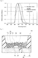
- the light-emitting device may have an emission spectrum with, for example, a first local maximum value P1 in a first peak wavelength in the range of 440 nm to 470 nm, a second local maximum value P2 in a second peak wavelength in the range of 490 nm to 540 nm, and a third local maximum value P3 in a third peak wavelength in the range of 570 nm to 650 nm.
- the emission spectrum may have a first local minimum value T1 between the first peak wavelength and the second peak wavelength, and a second local minimum value T2 between the second peak wavelength and the third peak wavelength.
- the first local maximum value P1 is attributable to, for example, the synthesis light of the light-emitting element and the emission spectrum of the first fluorescent material.
- the second local maximum value P2 is attributable to, for example, the emission spectrum of the first fluorescent material.
- the third local maximum value P3 is attributable to, for example, the emission spectrum of the third fluorescent material.
- the light-emitting device with a correlated color temperature of 3500 K to less than 4500 K may have an emission spectrum in which the ratio of the second local minimum value T2 to the second local maximum value P2, or T2/P2, may be, for example, 0.7 to 0.99, and preferably 0.8 to 0.99.
- the ratio T2/P2 may be, for example, 0.6 to 0.97, and preferably 0.65 to 0.96 in the light-emitting device with a correlated color temperature of 4500 K to less than 5700 K.
- the ratio T2/P2 may be, for example, 0.6 to 0.97, and preferably 0.7 to 0.95 in the light-emitting device with a correlated color temperature of 5700 K to 7200 K.
- the local maximum value or the local minimum value in an emission spectrum means an emission intensity relative to a wavelength at which the rate of change in the emission intensity relative to the wavelength is 0.
- the value is determined as a local maximum value.
- the value is determined as a local minimum value. If the rate of change in the emission intensity relative to the wavelength is 0 without positive to negative or negative to positive value change in the emission intensity before and after the wavelength, the value is neither a local maximum value or a local minimum value.
- the emission spectrum forms a mountain shape with a local maximum value as its peak, and a valley shape with a local minimum value as its deepest point.
- the light-emitting device with a correlated color temperature of 3500 K to less than 4500 K may have an emission spectrum with a ratio of the first local maximum value P1 to the second local maximum value P2, or P1/P2, of, for example, 1.4 to 1.8, and preferably 1.45 to 1.75.
- the ratio P1/P2 may be, for example, 1.4 to 2.19, and preferably 1.55 to 2.1 in the light-emitting device with a correlated color temperature of 4500 K to less than 5700 K.
- the ratio P1/P2 may be 2.0 to 2.7, preferably 2.05 to 2.5 in the light-emitting device with a correlated color temperature of 5700 K to 7200 K.
- the emission spectrum may contain more blue-green components. This enables, for example, the light-emitting device to compensate for the impaired blue color vision of aged people.
- the lighting tool includes at least one of the light-emitting devices described above, and may further include a reflection member, a protection member, and an attachment that provides electricity to the light-emitting device.
- the lighting tool may include a plurality of the light-emitting devices.
- the lighting tool may include a plurality of the same light-emitting devices, or a plurality of the light-emitting devices with, for example, different correlated color temperatures.
- the lighting tool may include a drive that individually drives a plurality of the light-emitting devices, and adjusts the luminosity and the correlated color temperature as appropriate.
- the lighting tool may be used as, for example, a direct-mounted, flush-mounted, or pendant light.
- alkaline-earth metal aluminate (hereinafter also referred to as "SAE") having a composition represented by formula (1a'), and an alkaline-earth metal halosilicate having a composition represented by formula (1b') (hereinafter also referred to as "chlorosilicate”) were prepared.
- SAE alkaline-earth metal aluminate
- chlorosilicate an alkaline-earth metal halosilicate having a composition represented by formula (1b')
- the reflectance spectrum of the prepared SAE was measured.
- the maximum value in the range of 380 nm to 435 nm of the relative reflectance was 8.9% as a value at 435 nm, which is not more than 30%.
- the maximum value of the relative reflectance of chlorosilicate in the range of 380 nm to 435 nm was 14.8% as a value at 435 nm.
- the SAE had a peak light-emitting wavelength of 495 nm, and a half bandwidth of 60 nm, and the chlorosilicate had a peak light-emitting wavelength of 510 nm, and a half bandwidth of 55 nm.
- an aluminium garnet fluorescent material having a composition represented by formula (2B) below was prepared.
- the prepared second fluorescent material had a peak light-emitting wavelength of 547 nm, and a half bandwidth of 109 nm.
- fluorescent materials SCASN 1, SCASN 2, SCASN 3, SCASN 4, SCASN 5, and SCASN 6 having a composition represented by formula (3C) were prepared.
- SCASN 1 had a peak light-emitting wavelength of 610 nm, and a half bandwidth of 72 nm.
- SCASN 2 had a peak light-emitting wavelength of 620 nm, and a half bandwidth of 75 nm.
- SCASN 3 had a peak light-emitting wavelength of 625 nm, and a half bandwidth of 78 nm.
- SCASN 4 had a peak light-emitting wavelength of 630 nm, and a half bandwidth of 82 nm.
- SCASN 5 had a peak light-emitting wavelength of 608 nm, and a half bandwidth of 72 nm.
- SCASN 6 had a peak light-emitting wavelength of 627 nm, and a half bandwidth of 75 nm.
- the fluorescent material 70 and silicone resin were mixed and dispersed, and then defoamed to have a fluorescent material-containing resin composition.
- the fluorescent material-containing resin composition contained the fluorescent materials 50.2% by mass in total relative to resin (taken as 100% by mass).
- the respective fluorescent material contents relative to the sum of the fluorescent materials were as follows: SAE as the first fluorescent material 71 was 59.7% by mass, the second fluorescent material 72 was 34.7% by mass, and SCASN 1 as the third fluorescent material 73 was 5.5% by mass.
- a molded body 40 having a recess was then prepared.
- a light-emitting element having a peak light-emitting wavelength of 450 nm and including a gallium nitride compound semiconductor was disposed in the recess, and the fluorescent material-containing resin composition was poured over the light-emitting element 10 to fill the recess, and then heated to be cured.
- a light-emitting device of Example 1 was prepared.
- the chromaticity coordinates correspond to about 6500 K correlated color temperature of the light-emitting device, which falls in the correlated color temperature in the range of 5700 K to 7200 K.
- a light-emitting device was produced in the same manner as in Example 1 except that the respective fluorescent material contents relative to the sum of the fluorescent materials were changed as shown in Table 1.
- a light-emitting device was produced in the same manner as in Example 1 except that the third fluorescent material 73 was changed to a mixture of SCASN 2 and SCASN 3 at a ratio of 50:50, and that the total fluorescent material content and the respective fluorescent material contents were changed as shown in Table 1.
- Table 1 Fluorescent material content (mass %) Content relative to resin (mass %) First fluorescent material Second fluorescent material Third fluorescent material Comparative Example 1 12.7 85.3 2.0 51.2
- Example 2 76.1 18.5 5.4 65.7
- a light-emitting device was produced in the same manner as in Example 3 except that the third fluorescent material 73 was changed to a mixture of SCASN 2 and SCASN 3 at a ratio of 50:50, and that the total fluorescent material content and the respective fluorescent material contents were changed as shown in Table 2.
- the chromaticity coordinates correspond to a correlated color temperature of the light-emitting device of about 4000 K, which falls in the correlated color temperature range of 3500 K to less than 4500 K.
- a light-emitting device was produced in the same manner as in Example 7 except that the third fluorescent material was changed to SCASN 2, and that the total fluorescent material content and the respective fluorescent material contents were changed as shown in Table 3.
- a light-emitting device was produced in the same manner as in Example 7 except that the third fluorescent material was changed to SCASN 6, and that the total fluorescent material content and the respective fluorescent material contents were changed as shown in Table 3.
- a light-emitting device was produced in the same manner as in Example 7 except that the third fluorescent material was changed to SCASN 4, and that the total fluorescent material content and the respective fluorescent material contents were changed as shown in Table 3.
- a light-emitting device was produced in the same manner as in Example 7 except that the third fluorescent material was changed to SCASN 6, and that the total fluorescent material content and the respective fluorescent material contents were changed as shown in Table 3.
- Table 3 Fluorescent material content (mass %) Content relative to resin (mass %) First fluorescent material Second fluorescent material Third fluorescent material Comparative Example 5 0.0 95.5 4.5 62.0 Comparative Example 6 28.7 68.3 3.0 69.7 Example 7 75.5 12.3 12.3 106.0
- a light-emitting device was produced in the same manner as in Example 11 except that the third fluorescent material was changed to SCASN 4, and that the total fluorescent material content and the respective fluorescent material contents were changed as shown in Table 4.
- a light-emitting device was produced in the same manner as in Example 11 except that the third fluorescent material was changed to SCASN 3, and that the total fluorescent material content and the respective fluorescent material contents were changed as shown in Table 4.
- a light-emitting device was produced in the same manner as in Example 11 except that the third fluorescent material was changed to SCASN 4, and that the total fluorescent material content and the respective fluorescent material contents were changed as shown in Table 4.
- a light-emitting device was produced in the same manner as in Example 11 except that the third fluorescent material was changed to SCASN 4, and that the total fluorescent material content and the respective fluorescent material contents were changed as shown in Table 4.
- Table 4 Fluorescent material content (mass %) Content relative to resin (mass %) First fluorescent material Second fluorescent material Third fluorescent material Comparative Example 7 0.0 93.9 6.2 88.5 Comparative Example 8 29.7 65.3 5.0 100.9 Example 11 45.7 48.7 5.6 109.4
- Example 12 47.0 48.0 5.0 106.4
- Example 13 46.9 48.3 4.7 106.6
- chromaticity coordinates, correlated color temperature, average color rendering index Ra, and special color rendering index R9 (as color rendering index) of emission color were obtained.
- the luminous flux and emission spectrum of each light-emitting device were measured using an integrating sphere. Each measured spectral distribution was multiplied by the action function of blue-light retinal damage, and then integrated in the wavelength range of 300 nm to 700 nm to obtain the effective radiant intensity for blue-light retinal damage.
- each spectral distribution was multiplied by the action function of melatonin secretion suppression, and then integrated in the wavelength range of 400 nm to 700 nm to obtain the effective radiant intensity for melatonin secretion suppression.
- the ratio of effective radiant intensity for melatonin secretion suppression to the effective radiant intensity for blue-light retinal damage was calculated, and used as the effective radiant intensity ratio.
- a light-emitting device that serves as a reference was selected for each correlated color temperature to calculate a relative luminous flux using the luminous flux of the reference light-emitting device as a reference.
- a spectral distribution was obtained by converting the luminous fluxes to have the same value.
- the spectral distribution after the conversion was used to calculate the effective radiant intensity for blue-light retinal damage, and the effective radiant intensity for melatonin secretion suppression. Further, the resultant values were normalized with respect to the effective radiant intensity of the reference light-emitting device for each correlated color temperature. The relative effective radiant intensities, when luminous fluxes were converted to have the same value, of blue-light retinal damage and melatonin secretion suppression were calculated. The results are shown in Tables 5 to 8 for each correlated color temperature of the light-emitting device.
- the respective emission spectra normalized by the peak light emitting intensity of the reference light-emitting device for the respective correlated color temperatures of the light-emitting devices are shown in Figs. 3 to 6 .
- the ratio of the second local minimum value T2 to the second local maximum value P2, or T2/P2, and the ratio of the first local maximum value P1 to the second local maximum value P2, or P1/P2, were calculated from each emission spectrum, and are shown in Tables 5 to 7.
- the mark "-" in these tables indicates that the local maximum or local minimum value was not clear, and the ratio was unable to be calculated.
Landscapes
- Chemical & Material Sciences (AREA)
- Inorganic Chemistry (AREA)
- Engineering & Computer Science (AREA)
- Materials Engineering (AREA)
- Organic Chemistry (AREA)
- Luminescent Compositions (AREA)
- Led Device Packages (AREA)
Applications Claiming Priority (1)
| Application Number | Priority Date | Filing Date | Title |
|---|---|---|---|
| JP2017188523A JP6940764B2 (ja) | 2017-09-28 | 2017-09-28 | 発光装置 |
Publications (2)
| Publication Number | Publication Date |
|---|---|
| EP3461873A1 EP3461873A1 (en) | 2019-04-03 |
| EP3461873B1 true EP3461873B1 (en) | 2020-10-21 |
Family
ID=63685672
Family Applications (1)
| Application Number | Title | Priority Date | Filing Date |
|---|---|---|---|
| EP18196805.8A Active EP3461873B1 (en) | 2017-09-28 | 2018-09-26 | Light-emitting device |
Country Status (4)
| Country | Link |
|---|---|
| US (2) | US10818827B2 (enExample) |
| EP (1) | EP3461873B1 (enExample) |
| JP (1) | JP6940764B2 (enExample) |
| CN (1) | CN109599473B (enExample) |
Families Citing this family (11)
| Publication number | Priority date | Publication date | Assignee | Title |
|---|---|---|---|---|
| KR102423748B1 (ko) * | 2015-07-08 | 2022-07-22 | 쑤저우 레킨 세미컨덕터 컴퍼니 리미티드 | 발광장치 |
| JP6940764B2 (ja) | 2017-09-28 | 2021-09-29 | 日亜化学工業株式会社 | 発光装置 |
| US10788709B2 (en) * | 2018-10-30 | 2020-09-29 | Innolux Corporation | Lighting device |
| CN111755429B (zh) | 2019-03-29 | 2024-07-09 | 日亚化学工业株式会社 | 发光装置 |
| US10971660B2 (en) * | 2019-08-09 | 2021-04-06 | Eyesafe Inc. | White LED light source and method of making same |
| JP7510068B2 (ja) * | 2019-10-30 | 2024-07-03 | 日亜化学工業株式会社 | 照明灯具、調光制御システム |
| JP7824502B2 (ja) * | 2020-03-31 | 2026-03-05 | 日亜化学工業株式会社 | 発光装置及びそれを備えた灯具 |
| JP7185146B2 (ja) | 2020-09-15 | 2022-12-07 | 日亜化学工業株式会社 | 発光装置 |
| KR20220094290A (ko) | 2020-12-28 | 2022-07-06 | 삼성전자주식회사 | 백색 발광장치 및 조명 장치 |
| JP7464959B1 (ja) | 2022-12-27 | 2024-04-10 | 三菱ケミカル株式会社 | 発光装置、照明装置、画像表示装置及び車両用表示灯 |
| CN119450844B (zh) * | 2024-12-02 | 2025-11-28 | 中国计量科学研究院 | 发光二极管的峰值波长调整方法、装置、设备及介质 |
Family Cites Families (65)
| Publication number | Priority date | Publication date | Assignee | Title |
|---|---|---|---|---|
| JPS607344B2 (ja) | 1976-03-08 | 1985-02-23 | 株式会社東芝 | カラー受像管 |
| CN1203557C (zh) | 2000-05-29 | 2005-05-25 | 电灯专利信托有限公司 | 基于发光二极管的发射白光的照明设备 |
| DE10026435A1 (de) | 2000-05-29 | 2002-04-18 | Osram Opto Semiconductors Gmbh | Kalzium-Magnesium-Chlorosilikat-Leuchtstoff und seine Anwendung bei Lumineszenz-Konversions-LED |
| AT410266B (de) | 2000-12-28 | 2003-03-25 | Tridonic Optoelectronics Gmbh | Lichtquelle mit einem lichtemittierenden element |
| US7611641B2 (en) | 2004-02-20 | 2009-11-03 | Koninklijke Philips Electronics N.V. | Illumination system comprising a radiation source and a fluorescent material |
| JPWO2006077740A1 (ja) | 2004-12-28 | 2008-06-19 | 日亜化学工業株式会社 | 発光装置及びその製造方法 |
| JP2006253336A (ja) | 2005-03-10 | 2006-09-21 | Toyoda Gosei Co Ltd | 光源装置 |
| EP1865564B1 (en) | 2005-03-18 | 2014-11-19 | Mitsubishi Chemical Corporation | Light-emitting device, white light-emitting device, illuminator, and image display |
| KR100682874B1 (ko) | 2005-05-02 | 2007-02-15 | 삼성전기주식회사 | 백색 led |
| JP2007049114A (ja) | 2005-05-30 | 2007-02-22 | Sharp Corp | 発光装置とその製造方法 |
| JP2008544553A (ja) | 2005-06-23 | 2008-12-04 | レンセレイアー ポリテクニック インスティテュート | 短波長ledとダウンコンバージョン物質で白色光を生成するパッケージ設計 |
| EP1935958A4 (en) | 2005-08-10 | 2010-10-27 | Mitsubishi Chem Corp | FLUORESCENT AND LIGHT-EMITTING DEVICE BASED ON IT |
| JPWO2009028657A1 (ja) * | 2007-08-30 | 2010-12-02 | 日亜化学工業株式会社 | 発光装置 |
| JP2009167338A (ja) | 2008-01-18 | 2009-07-30 | Sharp Corp | 波長変換部材およびこれを備える発光装置、ならびに蛍光体 |
| JP2009206459A (ja) | 2008-02-29 | 2009-09-10 | Sharp Corp | 色変換部材およびそれを用いた発光装置 |
| US7990045B2 (en) | 2008-03-15 | 2011-08-02 | Sensor Electronic Technology, Inc. | Solid-state lamps with partial conversion in phosphors for rendering an enhanced number of colors |
| US20090231832A1 (en) | 2008-03-15 | 2009-09-17 | Arturas Zukauskas | Solid-state lamps with complete conversion in phosphors for rendering an enhanced number of colors |
| JP2009245981A (ja) | 2008-03-28 | 2009-10-22 | Toyota Central R&D Labs Inc | Led発光装置 |
| WO2010098141A1 (ja) | 2009-02-26 | 2010-09-02 | 日亜化学工業株式会社 | 蛍光体及びその製造方法並びにこれを用いた発光装置 |
| KR101077990B1 (ko) | 2010-02-12 | 2011-10-31 | 삼성엘이디 주식회사 | 형광체, 발광장치, 면광원장치, 디스플레이 장치 및 조명장치 |
| US8508127B2 (en) | 2010-03-09 | 2013-08-13 | Cree, Inc. | High CRI lighting device with added long-wavelength blue color |
| KR101215342B1 (ko) | 2010-09-20 | 2012-12-26 | 삼성전자주식회사 | 사이알론 형광체, 그 제조방법 및 이를 이용한 발광소자 패키지 |
| US8404153B2 (en) | 2010-12-17 | 2013-03-26 | General Electric Company | White persistent phosphor blend or layered structure |
| EP3176838B1 (en) * | 2011-03-15 | 2019-01-30 | Kabushiki Kaisha Toshiba | White light source |
| JP5770269B2 (ja) * | 2011-04-22 | 2015-08-26 | 株式会社東芝 | 白色光源およびそれを用いた白色光源システム |
| JP2013033916A (ja) | 2011-06-28 | 2013-02-14 | Sharp Corp | 発光装置及びその製造方法 |
| US8704440B2 (en) | 2011-07-06 | 2014-04-22 | Osram Sylvania Inc. | LED lighting device having a phosphor composition |
| KR20130014256A (ko) | 2011-07-29 | 2013-02-07 | 엘지이노텍 주식회사 | 발광 소자 패키지 및 이를 이용한 조명 시스템 |
| TWI464241B (zh) | 2011-08-02 | 2014-12-11 | 億光電子工業股份有限公司 | 螢光粉組成及使用該螢光粉組成的白色發光裝置 |
| EP4044264B1 (en) | 2011-10-24 | 2024-01-03 | Seoul Semiconductor Co., Ltd. | White light source and white light source system using white light source |
| JP6189217B2 (ja) * | 2011-11-07 | 2017-08-30 | 株式会社東芝 | 白色光源およびそれを用いた白色光源システム |
| TW201320412A (zh) | 2011-11-14 | 2013-05-16 | 長榮光電股份有限公司 | 發光二極體封裝 |
| JP5927557B2 (ja) * | 2012-05-11 | 2016-06-01 | パナソニックIpマネジメント株式会社 | 照明装置 |
| TWI497688B (zh) * | 2012-12-27 | 2015-08-21 | 財團法人工業技術研究院 | 照明裝置及其光源模組 |
| JP2014170082A (ja) | 2013-03-02 | 2014-09-18 | Masao Iijima | Led照明光フィルタ及びled照明装置 |
| US9142732B2 (en) | 2013-03-04 | 2015-09-22 | Osram Sylvania Inc. | LED lamp with quantum dots layer |
| KR102075982B1 (ko) | 2013-03-15 | 2020-02-12 | 삼성전자주식회사 | 반도체 발광소자 패키지 |
| JP6853614B2 (ja) | 2013-03-29 | 2021-03-31 | 株式会社朝日ラバー | Led照明装置、その製造方法及びled照明方法 |
| JPWO2015002139A1 (ja) | 2013-07-03 | 2017-02-23 | デンカ株式会社 | 蛍光体及び発光装置 |
| KR20150007885A (ko) | 2013-07-12 | 2015-01-21 | 엘지이노텍 주식회사 | 형광체 및 이를 구비한 발광 소자 |
| JP6380826B2 (ja) | 2013-09-20 | 2018-08-29 | パナソニックIpマネジメント株式会社 | 光源装置 |
| JP2015070866A (ja) * | 2013-10-01 | 2015-04-16 | パナソニックIpマネジメント株式会社 | 光源モジュール及び照明装置 |
| WO2015050317A1 (ko) | 2013-10-02 | 2015-04-09 | 지엘비텍 주식회사 | 고연색성 백색 발광 소자 |
| JP2015082596A (ja) * | 2013-10-23 | 2015-04-27 | 株式会社東芝 | 発光装置 |
| JP6195117B2 (ja) | 2013-12-03 | 2017-09-13 | パナソニックIpマネジメント株式会社 | 酸塩化物蛍光体、発光装置、照明装置、及び車両 |
| JP6273463B2 (ja) | 2013-12-03 | 2018-02-07 | パナソニックIpマネジメント株式会社 | 蛍光体材料および発光装置 |
| JP2015113358A (ja) | 2013-12-09 | 2015-06-22 | 三菱化学株式会社 | 蛍光体、蛍光体含有組成物、発光装置、照明装置、画像表示装置、及び蛍光体の製造方法 |
| JP6278305B2 (ja) * | 2013-12-12 | 2018-02-14 | パナソニックIpマネジメント株式会社 | 光源モジュール |
| JP2015115506A (ja) * | 2013-12-12 | 2015-06-22 | パナソニックIpマネジメント株式会社 | 照明光源 |
| JP6548104B2 (ja) * | 2013-12-12 | 2019-07-24 | パナソニックIpマネジメント株式会社 | 光源モジュール及び光源ユニット |
| JP6528418B2 (ja) | 2014-01-29 | 2019-06-12 | 日亜化学工業株式会社 | 蛍光体及びこれを用いた発光装置 |
| JP6287268B2 (ja) | 2014-01-29 | 2018-03-07 | 日亜化学工業株式会社 | 発光装置 |
| JP6156440B2 (ja) * | 2014-05-30 | 2017-07-05 | 日亜化学工業株式会社 | 赤色発光蛍光体及びこれを用いた発光装置 |
| JP6365159B2 (ja) * | 2014-09-16 | 2018-08-01 | 日亜化学工業株式会社 | 発光装置 |
| JP6877342B2 (ja) * | 2014-12-16 | 2021-05-26 | シグニファイ ホールディング ビー ヴィSignify Holding B.V. | 照明装置、照明システム、並びに前記照明装置及び前記照明システムの使用 |
| CN107427687B (zh) * | 2015-03-19 | 2019-11-01 | 飞利浦照明控股有限公司 | 一种照明装置及其用途 |
| JP6544082B2 (ja) | 2015-06-30 | 2019-07-17 | 日亜化学工業株式会社 | 発光装置 |
| JP6526603B2 (ja) * | 2015-06-30 | 2019-06-05 | 日亜化学工業株式会社 | 発光装置 |
| US9735323B2 (en) * | 2015-06-30 | 2017-08-15 | Nichia Corporation | Light emitting device having a triple phosphor fluorescent member |
| JP6115611B2 (ja) * | 2015-10-22 | 2017-04-19 | 住友大阪セメント株式会社 | 光半導体発光装置、照明器具、及び表示装置 |
| JP6460040B2 (ja) * | 2016-03-04 | 2019-01-30 | 日亜化学工業株式会社 | 発光装置 |
| US10256374B2 (en) * | 2016-03-04 | 2019-04-09 | Nichia Corporation | Light emitting device |
| JP2017183522A (ja) | 2016-03-30 | 2017-10-05 | サンケン電気株式会社 | 発光装置 |
| JP6233668B2 (ja) | 2016-06-01 | 2017-11-22 | パナソニックIpマネジメント株式会社 | 光源装置 |
| JP6940764B2 (ja) | 2017-09-28 | 2021-09-29 | 日亜化学工業株式会社 | 発光装置 |
-
2017
- 2017-09-28 JP JP2017188523A patent/JP6940764B2/ja active Active
-
2018
- 2018-09-26 US US16/142,586 patent/US10818827B2/en active Active
- 2018-09-26 EP EP18196805.8A patent/EP3461873B1/en active Active
- 2018-09-27 CN CN201811129966.XA patent/CN109599473B/zh active Active
-
2020
- 2020-09-22 US US17/028,496 patent/US11605761B2/en active Active
Non-Patent Citations (1)
| Title |
|---|
| None * |
Also Published As
| Publication number | Publication date |
|---|---|
| US10818827B2 (en) | 2020-10-27 |
| CN109599473A (zh) | 2019-04-09 |
| JP2019067808A (ja) | 2019-04-25 |
| US11605761B2 (en) | 2023-03-14 |
| CN109599473B (zh) | 2023-02-28 |
| US20190097098A1 (en) | 2019-03-28 |
| US20210013383A1 (en) | 2021-01-14 |
| JP6940764B2 (ja) | 2021-09-29 |
| EP3461873A1 (en) | 2019-04-03 |
Similar Documents
| Publication | Publication Date | Title |
|---|---|---|
| EP3461873B1 (en) | Light-emitting device | |
| US9711686B2 (en) | Lighting device with plural fluorescent materials | |
| EP3893286B1 (en) | Light emitting device | |
| EP2535392B1 (en) | Halophosphate phosphor and white light-emitting device | |
| TWI718305B (zh) | 發光裝置 | |
| US7088038B2 (en) | Green phosphor for general illumination applications | |
| EP2540798A1 (en) | Halophosphate phosphor and white light emitting device | |
| US10243113B2 (en) | Light emitting device | |
| WO2005017066A1 (en) | Deep red phosphor for general illumination applications | |
| CN101138278A (zh) | 包括辐射源和荧光材料的照明系统 | |
| CN101194375A (zh) | 发光装置 | |
| US10806809B2 (en) | Light-emitting device | |
| US20160223147A1 (en) | Light emitting device | |
| EP3916073B1 (en) | Light emitting device | |
| JP7100269B2 (ja) | 発光装置およびその製造方法 | |
| US20210074891A1 (en) | Light emitting device | |
| JP7614531B2 (ja) | 発光装置およびその製造方法 |
Legal Events
| Date | Code | Title | Description |
|---|---|---|---|
| PUAI | Public reference made under article 153(3) epc to a published international application that has entered the european phase |
Free format text: ORIGINAL CODE: 0009012 |
|
| STAA | Information on the status of an ep patent application or granted ep patent |
Free format text: STATUS: THE APPLICATION HAS BEEN PUBLISHED |
|
| AK | Designated contracting states |
Kind code of ref document: A1 Designated state(s): AL AT BE BG CH CY CZ DE DK EE ES FI FR GB GR HR HU IE IS IT LI LT LU LV MC MK MT NL NO PL PT RO RS SE SI SK SM TR |
|
| AX | Request for extension of the european patent |
Extension state: BA ME |
|
| STAA | Information on the status of an ep patent application or granted ep patent |
Free format text: STATUS: REQUEST FOR EXAMINATION WAS MADE |
|
| 17P | Request for examination filed |
Effective date: 20190812 |
|
| RBV | Designated contracting states (corrected) |
Designated state(s): AL AT BE BG CH CY CZ DE DK EE ES FI FR GB GR HR HU IE IS IT LI LT LU LV MC MK MT NL NO PL PT RO RS SE SI SK SM TR |
|
| STAA | Information on the status of an ep patent application or granted ep patent |
Free format text: STATUS: EXAMINATION IS IN PROGRESS |
|
| 17Q | First examination report despatched |
Effective date: 20191108 |
|
| GRAP | Despatch of communication of intention to grant a patent |
Free format text: ORIGINAL CODE: EPIDOSNIGR1 |
|
| STAA | Information on the status of an ep patent application or granted ep patent |
Free format text: STATUS: GRANT OF PATENT IS INTENDED |
|
| INTG | Intention to grant announced |
Effective date: 20200227 |
|
| GRAJ | Information related to disapproval of communication of intention to grant by the applicant or resumption of examination proceedings by the epo deleted |
Free format text: ORIGINAL CODE: EPIDOSDIGR1 |
|
| STAA | Information on the status of an ep patent application or granted ep patent |
Free format text: STATUS: EXAMINATION IS IN PROGRESS |
|
| GRAS | Grant fee paid |
Free format text: ORIGINAL CODE: EPIDOSNIGR3 |
|
| STAA | Information on the status of an ep patent application or granted ep patent |
Free format text: STATUS: GRANT OF PATENT IS INTENDED |
|
| GRAP | Despatch of communication of intention to grant a patent |
Free format text: ORIGINAL CODE: EPIDOSNIGR1 |
|
| INTC | Intention to grant announced (deleted) | ||
| RIN1 | Information on inventor provided before grant (corrected) |
Inventor name: KONDO, MASAKI Inventor name: FUJIO, KAZUSHIGE |
|
| INTG | Intention to grant announced |
Effective date: 20200805 |
|
| GRAA | (expected) grant |
Free format text: ORIGINAL CODE: 0009210 |
|
| STAA | Information on the status of an ep patent application or granted ep patent |
Free format text: STATUS: THE PATENT HAS BEEN GRANTED |
|
| AK | Designated contracting states |
Kind code of ref document: B1 Designated state(s): AL AT BE BG CH CY CZ DE DK EE ES FI FR GB GR HR HU IE IS IT LI LT LU LV MC MK MT NL NO PL PT RO RS SE SI SK SM TR |
|
| REG | Reference to a national code |
Ref country code: GB Ref legal event code: FG4D |
|
| REG | Reference to a national code |
Ref country code: CH Ref legal event code: EP |
|
| REG | Reference to a national code |
Ref country code: DE Ref legal event code: R096 Ref document number: 602018008887 Country of ref document: DE |
|
| REG | Reference to a national code |
Ref country code: IE Ref legal event code: FG4D |
|
| REG | Reference to a national code |
Ref country code: AT Ref legal event code: REF Ref document number: 1325884 Country of ref document: AT Kind code of ref document: T Effective date: 20201115 |
|
| REG | Reference to a national code |
Ref country code: NL Ref legal event code: FP |
|
| REG | Reference to a national code |
Ref country code: AT Ref legal event code: MK05 Ref document number: 1325884 Country of ref document: AT Kind code of ref document: T Effective date: 20201021 |
|
| PG25 | Lapsed in a contracting state [announced via postgrant information from national office to epo] |
Ref country code: FI Free format text: LAPSE BECAUSE OF FAILURE TO SUBMIT A TRANSLATION OF THE DESCRIPTION OR TO PAY THE FEE WITHIN THE PRESCRIBED TIME-LIMIT Effective date: 20201021 Ref country code: RS Free format text: LAPSE BECAUSE OF FAILURE TO SUBMIT A TRANSLATION OF THE DESCRIPTION OR TO PAY THE FEE WITHIN THE PRESCRIBED TIME-LIMIT Effective date: 20201021 Ref country code: PT Free format text: LAPSE BECAUSE OF FAILURE TO SUBMIT A TRANSLATION OF THE DESCRIPTION OR TO PAY THE FEE WITHIN THE PRESCRIBED TIME-LIMIT Effective date: 20210222 Ref country code: GR Free format text: LAPSE BECAUSE OF FAILURE TO SUBMIT A TRANSLATION OF THE DESCRIPTION OR TO PAY THE FEE WITHIN THE PRESCRIBED TIME-LIMIT Effective date: 20210122 Ref country code: NO Free format text: LAPSE BECAUSE OF FAILURE TO SUBMIT A TRANSLATION OF THE DESCRIPTION OR TO PAY THE FEE WITHIN THE PRESCRIBED TIME-LIMIT Effective date: 20210121 |
|
| REG | Reference to a national code |
Ref country code: LT Ref legal event code: MG4D |
|
| PG25 | Lapsed in a contracting state [announced via postgrant information from national office to epo] |
Ref country code: SE Free format text: LAPSE BECAUSE OF FAILURE TO SUBMIT A TRANSLATION OF THE DESCRIPTION OR TO PAY THE FEE WITHIN THE PRESCRIBED TIME-LIMIT Effective date: 20201021 Ref country code: IS Free format text: LAPSE BECAUSE OF FAILURE TO SUBMIT A TRANSLATION OF THE DESCRIPTION OR TO PAY THE FEE WITHIN THE PRESCRIBED TIME-LIMIT Effective date: 20210221 Ref country code: PL Free format text: LAPSE BECAUSE OF FAILURE TO SUBMIT A TRANSLATION OF THE DESCRIPTION OR TO PAY THE FEE WITHIN THE PRESCRIBED TIME-LIMIT Effective date: 20201021 Ref country code: LV Free format text: LAPSE BECAUSE OF FAILURE TO SUBMIT A TRANSLATION OF THE DESCRIPTION OR TO PAY THE FEE WITHIN THE PRESCRIBED TIME-LIMIT Effective date: 20201021 Ref country code: BG Free format text: LAPSE BECAUSE OF FAILURE TO SUBMIT A TRANSLATION OF THE DESCRIPTION OR TO PAY THE FEE WITHIN THE PRESCRIBED TIME-LIMIT Effective date: 20210121 Ref country code: AT Free format text: LAPSE BECAUSE OF FAILURE TO SUBMIT A TRANSLATION OF THE DESCRIPTION OR TO PAY THE FEE WITHIN THE PRESCRIBED TIME-LIMIT Effective date: 20201021 Ref country code: ES Free format text: LAPSE BECAUSE OF FAILURE TO SUBMIT A TRANSLATION OF THE DESCRIPTION OR TO PAY THE FEE WITHIN THE PRESCRIBED TIME-LIMIT Effective date: 20201021 |
|
| PG25 | Lapsed in a contracting state [announced via postgrant information from national office to epo] |
Ref country code: HR Free format text: LAPSE BECAUSE OF FAILURE TO SUBMIT A TRANSLATION OF THE DESCRIPTION OR TO PAY THE FEE WITHIN THE PRESCRIBED TIME-LIMIT Effective date: 20201021 |
|
| REG | Reference to a national code |
Ref country code: DE Ref legal event code: R097 Ref document number: 602018008887 Country of ref document: DE |
|
| PG25 | Lapsed in a contracting state [announced via postgrant information from national office to epo] |
Ref country code: CZ Free format text: LAPSE BECAUSE OF FAILURE TO SUBMIT A TRANSLATION OF THE DESCRIPTION OR TO PAY THE FEE WITHIN THE PRESCRIBED TIME-LIMIT Effective date: 20201021 Ref country code: EE Free format text: LAPSE BECAUSE OF FAILURE TO SUBMIT A TRANSLATION OF THE DESCRIPTION OR TO PAY THE FEE WITHIN THE PRESCRIBED TIME-LIMIT Effective date: 20201021 Ref country code: SM Free format text: LAPSE BECAUSE OF FAILURE TO SUBMIT A TRANSLATION OF THE DESCRIPTION OR TO PAY THE FEE WITHIN THE PRESCRIBED TIME-LIMIT Effective date: 20201021 Ref country code: RO Free format text: LAPSE BECAUSE OF FAILURE TO SUBMIT A TRANSLATION OF THE DESCRIPTION OR TO PAY THE FEE WITHIN THE PRESCRIBED TIME-LIMIT Effective date: 20201021 Ref country code: SK Free format text: LAPSE BECAUSE OF FAILURE TO SUBMIT A TRANSLATION OF THE DESCRIPTION OR TO PAY THE FEE WITHIN THE PRESCRIBED TIME-LIMIT Effective date: 20201021 Ref country code: LT Free format text: LAPSE BECAUSE OF FAILURE TO SUBMIT A TRANSLATION OF THE DESCRIPTION OR TO PAY THE FEE WITHIN THE PRESCRIBED TIME-LIMIT Effective date: 20201021 |
|
| PLBE | No opposition filed within time limit |
Free format text: ORIGINAL CODE: 0009261 |
|
| STAA | Information on the status of an ep patent application or granted ep patent |
Free format text: STATUS: NO OPPOSITION FILED WITHIN TIME LIMIT |
|
| PG25 | Lapsed in a contracting state [announced via postgrant information from national office to epo] |
Ref country code: DK Free format text: LAPSE BECAUSE OF FAILURE TO SUBMIT A TRANSLATION OF THE DESCRIPTION OR TO PAY THE FEE WITHIN THE PRESCRIBED TIME-LIMIT Effective date: 20201021 |
|
| 26N | No opposition filed |
Effective date: 20210722 |
|
| PG25 | Lapsed in a contracting state [announced via postgrant information from national office to epo] |
Ref country code: IT Free format text: LAPSE BECAUSE OF FAILURE TO SUBMIT A TRANSLATION OF THE DESCRIPTION OR TO PAY THE FEE WITHIN THE PRESCRIBED TIME-LIMIT Effective date: 20201021 Ref country code: AL Free format text: LAPSE BECAUSE OF FAILURE TO SUBMIT A TRANSLATION OF THE DESCRIPTION OR TO PAY THE FEE WITHIN THE PRESCRIBED TIME-LIMIT Effective date: 20201021 |
|
| PG25 | Lapsed in a contracting state [announced via postgrant information from national office to epo] |
Ref country code: SI Free format text: LAPSE BECAUSE OF FAILURE TO SUBMIT A TRANSLATION OF THE DESCRIPTION OR TO PAY THE FEE WITHIN THE PRESCRIBED TIME-LIMIT Effective date: 20201021 |
|
| REG | Reference to a national code |
Ref country code: CH Ref legal event code: PL |
|
| REG | Reference to a national code |
Ref country code: BE Ref legal event code: MM Effective date: 20210930 |
|
| PG25 | Lapsed in a contracting state [announced via postgrant information from national office to epo] |
Ref country code: IS Free format text: LAPSE BECAUSE OF FAILURE TO SUBMIT A TRANSLATION OF THE DESCRIPTION OR TO PAY THE FEE WITHIN THE PRESCRIBED TIME-LIMIT Effective date: 20210221 Ref country code: MC Free format text: LAPSE BECAUSE OF FAILURE TO SUBMIT A TRANSLATION OF THE DESCRIPTION OR TO PAY THE FEE WITHIN THE PRESCRIBED TIME-LIMIT Effective date: 20201021 |
|
| PG25 | Lapsed in a contracting state [announced via postgrant information from national office to epo] |
Ref country code: LU Free format text: LAPSE BECAUSE OF NON-PAYMENT OF DUE FEES Effective date: 20210926 Ref country code: IE Free format text: LAPSE BECAUSE OF NON-PAYMENT OF DUE FEES Effective date: 20210926 Ref country code: BE Free format text: LAPSE BECAUSE OF NON-PAYMENT OF DUE FEES Effective date: 20210930 |
|
| PG25 | Lapsed in a contracting state [announced via postgrant information from national office to epo] |
Ref country code: LI Free format text: LAPSE BECAUSE OF NON-PAYMENT OF DUE FEES Effective date: 20210930 Ref country code: CH Free format text: LAPSE BECAUSE OF NON-PAYMENT OF DUE FEES Effective date: 20210930 |
|
| P01 | Opt-out of the competence of the unified patent court (upc) registered |
Effective date: 20230522 |
|
| PG25 | Lapsed in a contracting state [announced via postgrant information from national office to epo] |
Ref country code: CY Free format text: LAPSE BECAUSE OF FAILURE TO SUBMIT A TRANSLATION OF THE DESCRIPTION OR TO PAY THE FEE WITHIN THE PRESCRIBED TIME-LIMIT Effective date: 20201021 |
|
| PG25 | Lapsed in a contracting state [announced via postgrant information from national office to epo] |
Ref country code: HU Free format text: LAPSE BECAUSE OF FAILURE TO SUBMIT A TRANSLATION OF THE DESCRIPTION OR TO PAY THE FEE WITHIN THE PRESCRIBED TIME-LIMIT; INVALID AB INITIO Effective date: 20180926 |
|
| PG25 | Lapsed in a contracting state [announced via postgrant information from national office to epo] |
Ref country code: MK Free format text: LAPSE BECAUSE OF FAILURE TO SUBMIT A TRANSLATION OF THE DESCRIPTION OR TO PAY THE FEE WITHIN THE PRESCRIBED TIME-LIMIT Effective date: 20201021 |
|
| PG25 | Lapsed in a contracting state [announced via postgrant information from national office to epo] |
Ref country code: MT Free format text: LAPSE BECAUSE OF FAILURE TO SUBMIT A TRANSLATION OF THE DESCRIPTION OR TO PAY THE FEE WITHIN THE PRESCRIBED TIME-LIMIT Effective date: 20201021 |
|
| PGFP | Annual fee paid to national office [announced via postgrant information from national office to epo] |
Ref country code: NL Payment date: 20250814 Year of fee payment: 8 |
|
| PGFP | Annual fee paid to national office [announced via postgrant information from national office to epo] |
Ref country code: DE Payment date: 20250730 Year of fee payment: 8 |
|
| PGFP | Annual fee paid to national office [announced via postgrant information from national office to epo] |
Ref country code: GB Payment date: 20250807 Year of fee payment: 8 |
|
| PGFP | Annual fee paid to national office [announced via postgrant information from national office to epo] |
Ref country code: FR Payment date: 20250808 Year of fee payment: 8 |
|
| PG25 | Lapsed in a contracting state [announced via postgrant information from national office to epo] |
Ref country code: TR Free format text: LAPSE BECAUSE OF FAILURE TO SUBMIT A TRANSLATION OF THE DESCRIPTION OR TO PAY THE FEE WITHIN THE PRESCRIBED TIME-LIMIT Effective date: 20201021 |