EP3367168B1 - Electrophotographic photosensitive member, process cartridge, and electrophotographic apparatus - Google Patents
Electrophotographic photosensitive member, process cartridge, and electrophotographic apparatus Download PDFInfo
- Publication number
- EP3367168B1 EP3367168B1 EP18158550.6A EP18158550A EP3367168B1 EP 3367168 B1 EP3367168 B1 EP 3367168B1 EP 18158550 A EP18158550 A EP 18158550A EP 3367168 B1 EP3367168 B1 EP 3367168B1
- Authority
- EP
- European Patent Office
- Prior art keywords
- particles
- layer
- photosensitive member
- electrophotographic photosensitive
- resin
- Prior art date
- Legal status (The legal status is an assumption and is not a legal conclusion. Google has not performed a legal analysis and makes no representation as to the accuracy of the status listed.)
- Active
Links
Images

Classifications
-
- G—PHYSICS
- G03—PHOTOGRAPHY; CINEMATOGRAPHY; ANALOGOUS TECHNIQUES USING WAVES OTHER THAN OPTICAL WAVES; ELECTROGRAPHY; HOLOGRAPHY
- G03G—ELECTROGRAPHY; ELECTROPHOTOGRAPHY; MAGNETOGRAPHY
- G03G5/00—Recording-members for original recording by exposure, e.g. to light, to heat or to electrons; Manufacture thereof; Selection of materials therefor
- G03G5/14—Inert intermediate or cover layers for charge-receiving layers
- G03G5/147—Cover layers
-
- G—PHYSICS
- G03—PHOTOGRAPHY; CINEMATOGRAPHY; ANALOGOUS TECHNIQUES USING WAVES OTHER THAN OPTICAL WAVES; ELECTROGRAPHY; HOLOGRAPHY
- G03G—ELECTROGRAPHY; ELECTROPHOTOGRAPHY; MAGNETOGRAPHY
- G03G5/00—Recording-members for original recording by exposure, e.g. to light, to heat or to electrons; Manufacture thereof; Selection of materials therefor
- G03G5/14—Inert intermediate or cover layers for charge-receiving layers
- G03G5/142—Inert intermediate layers
- G03G5/144—Inert intermediate layers comprising inorganic material
-
- G—PHYSICS
- G03—PHOTOGRAPHY; CINEMATOGRAPHY; ANALOGOUS TECHNIQUES USING WAVES OTHER THAN OPTICAL WAVES; ELECTROGRAPHY; HOLOGRAPHY
- G03G—ELECTROGRAPHY; ELECTROPHOTOGRAPHY; MAGNETOGRAPHY
- G03G5/00—Recording-members for original recording by exposure, e.g. to light, to heat or to electrons; Manufacture thereof; Selection of materials therefor
- G03G5/16—Layers for recording by changing the magnetic properties, e.g. for Curie-point-writing
Definitions
- the present disclosure relates to an electrophotographic photosensitive member, and a process cartridge and an electrophotographic apparatus each including the electrophotographic photosensitive member.
- Electrophotographic photosensitive members including a layer containing a ferroelectric material are also known as disclosed in Japanese Patent Laid-Open No. 11-109669 and Japanese Patent No. 2879084 .
- Japanese Patent Laid-Open No. 11-109669 discloses that an electrophotographic photosensitive member including a protective layer containing ferroelectric particles can be uniformly charged due to polarization.
- Japanese Paten No. 2879084 discloses an electrophotographic photosensitive member including an intermediate layer containing at least one compound selected from the group consisting of tantalates, titanates, and niobates.
- WO 2011/027912 A1 discloses an electrophotographic photosensitive member comprising a support member; an electroconductive layer; and a photosensitive layer in this order, wherein the electroconductive layer contains a binder and particles, the particles each including a core made of metal oxides selected from a list comprising lithium niobate particles, potassium niobate particles and lithium tantalate particles, and a coating layer coating the core comprising electrically conductive metal oxide, including tin-doped indium oxide particles, aluminum-doped zinc oxide particles and phosphorus-doped tin oxide particles, tungsten-doped tin oxide particles, and fluorine-doped tin oxide particles.
- the electroconductive layer contains a binder and particles, the particles each including a core made of metal oxides selected from a list comprising lithium niobate particles, potassium niobate particles and lithium tantalate particles, and a coating layer coating the core comprising electrically conductive metal oxide, including tin
- the present invention in its first aspect provides an electrophotographic photosensitive member as specified in claims 1 to 5.
- the present invention in its second aspect provides a process cartridge as specified in claim 6.
- the present invention in its third aspect provides an electrophotographic apparatus as specified in claim 7.
- the electrophotographic photosensitive member according to the present disclosure can be uniformly charged and keep potential stable in repeated use.
- the electrophotographic photosensitive member disclosed in Japanese Patent Laid-Open No. 11-109669 and Japanese Patent No. 2879084 cannot be uniformly charged nor keep potential stable in repeated use.
- the electrophotographic photosensitive member disclosed in Japanese Patent Laid-Open No. 11-109669 includes a protective layer containing ferroelectric particles that are generally insulative. These particles act as a carrier trap that restricts the flow of charge carriers in some cases, and accordingly, the electrophotographic photosensitive member does not satisfactorily keep potential stable when used repeatedly. If the thickness of the protective layer is reduced, the ferroelectric particles do not produce the intended effect of increasing dielectric relaxation, and, consequently, uniformity of charged potential is reduced.
- the intermediate layer does not have a sufficient electrical conductivity, and the potential stability of the photosensitive member is insufficient in repeated use.
- the present disclosure provides an electrophotographic photosensitive member that can be uniformly charged and keep potential stable in repeated use.
- the present inventors have found through their studies that when the known electrophotographic photosensitive member passes through the nip region with the charging roller for being charged, the discharge (downstream discharge) that occurs between the charging roller and the surface of the photosensitive member on the downstream side of the nip region becomes unstable, depending on the scheme for charging (for example, under a charging scheme mainly using the direct current component). It has been found that the unstable downstream discharge makes charged potential nonuniform, consequently causing problems with image quality, such as streaks formed in the resulting image. Such problems occur markedly in repeated use.
- the present inventors have studied for solving such problems and found that it is effective in stabilizing downstream discharge to increase the attenuation of charged potential when the photosensitive member passes through the nip region. It has also been found that for this purpose, it is desirable that dielectric relaxation be increased by adding specific particles to the electroconductive layer.
- dielectric relaxation can be increased, and electric conductivity can be improved. The mechanism of this can be explained as below.
- the ferroelectric material used as the core material of the particles contained in the electroconductive layer increases the dielectric relaxation of the electrophotographic photosensitive member and promotes the attenuation of charged potential when the photosensitive member passes through the nip region.
- the electrically conductive material in the coating layer of the particle enhances the electrical conductivity of the electroconductive layer, relieves the increase of residual potential in image formation, keeps dark and bright portion potentials from fluctuating, and keeps potential stable in repeated use.
- the ferroelectric material can be prevented from acting as a carrier trap.
- Electrophotographic Photosensitive Member Such synergistic interaction between components or members of the electrophotographic photosensitive member enables the photosensitive member to be uniformly charged and keep potential stable in repeated use.
- the electrophotographic photosensitive member disclosed herein includes a support member, an electroconductive layer, and a photosensitive layer in this order.
- the electrophotographic photosensitive member may be manufactured by applying each of the coating liquids prepared for forming the respective layers, which will be described later, in a desired order, and drying the coatings.
- Each coating liquid may be applied by dip coating, spray coating, ink jet coating, roll coating, die coating, blade coating, curtain coating, wire bar coating, ring coating, or any other method.
- dip coating may be employed from the viewpoint of efficiency and productivity.
- the electrophotographic photosensitive member disclosed herein includes a support member.
- the support member is electrically conductive.
- the support member may be in the form of a cylinder, a belt, a sheet, or the like.
- a cylindrical support member is beneficial.
- the support member may be surface-treated by electrochemical treatment, such as anodization, or blasting, or cutting.
- the support member may be made of a metal, a resin, or glass.
- an electrically conductive material may be added into or applied over the support member to impart an electrical conductivity.
- M 1 can represent an element selected from the group consisting of Sr, Li, Na, K, and Ba
- M 2 can represent an element selected from the group consisting of Ti, Nb, Ta, and Zr.
- the substance forming the core is a ferroelectric material represented by general formula (1) and may be any one selected from among strontium titanate (SrTiO 3 ), barium titanate (BaTiO 3 ), and strontium niobate in view of stability in forming the coating layer and electrical conductivity. In some embodiments, SrTiO 3 or BaTiO 3 may be used.
- tin oxide used as the electrically conductive material, tin oxide may be doped with an element selected from the group consisting of niobium, tantalum, phosphorus, tungsten, and fluorine. If zinc oxide is used, zinc oxide may be doped with either aluminum or gallium. If tantalum oxide is used, titanium oxide may be doped with either niobium or tantalum.
- the content of dopant added to the coating layer may be in the range of 0.5% by mass to 10.0% by mass relative to the total mass of the coating layer. If the dopant content is less than 0.5% by mass, the potential fluctuation at dark and bright portions may not be sufficiently reduced in some cases. In contrast, if the dopant content is higher than 10.0% by mass, leakage current may often occur in the electrophotographic photosensitive member. In an embodiment, the dopant content may be in the range of 1.0% by mass to 7.0% by mass relative to the total mass of the coating layer.
- the particles may have an average primary particle size (Di) in the range of 0.05 ⁇ m to 0.50 ⁇ m. Particles having an average primary particle size of 0.05 ⁇ m or more are unlikely to aggregate in the coating liquid prepared for forming the electroconductive layer (hereinafter may be referred to as electroconductive layer-forming coating liquid). Aggregates of the particles in the coating liquid reduce the stability of the coating liquid and cause the resulting electroconductive layer to crack in the surface thereof. If particles having an average primary particle size of 0.50 ⁇ m or less are used, the surface of the resulting electroconductive layer is unlikely to become rough. A rough surface of the electroconductive layer easily causes local charge carrier injection into the photosensitive layer. Consequently, black spots are likely to become noticeable in a white or blank area in the output image. More beneficially, the average primary particle size of the particles is in the range of 0.07 ⁇ m to 0.40 ⁇ m.
- the average diameter of the core may be 1 time to 50 times, beneficially 5 times to 20 times, as large as the average thickness of the coating layer. Such particles are beneficial for further stabilizing potential in repeated use.
- the average thickness of the coating layer may be 5 nm or more.
- the particles may be surface-treated with a silane coupling agent or the like.
- the particle content in the electroconductive layer may be in the range of 20% by volume to 50% by volume relative to the total volume of the electroconductive layer.
- the particle content is less than 20% by volume, the distance between the particles increases and, accordingly, the volume resistivity of the electroconductive layer tends to increase.
- the particle content is more than 50% by volume, the distance between the particles decreases and, accordingly, the particles become likely to come into contact with each other. In this instance, particles in contact with each other locally reduce the volume resistivity of the electroconductive layer, tending to cause leakage in the electrophotographic photosensitive member.
- the particle content in the electroconductive layer may be in the range of 30% by volume to 45% by volume relative to the total volume of the electroconductive layer.
- the electroconductive layer may further contain a different type of electrically conductive particles.
- the material of the further added electrically conductive particles may be a metal oxide, a metal, carbon black, or the like.
- metal oxide examples include zinc oxide, aluminum oxide, indium oxide, silicon oxide, zirconium oxide, tin oxide, titanium oxide, magnesium oxide, antimony oxide, and bismuth oxide.
- metal oxide examples include aluminum, nickel, iron, nichrome, copper, zinc, and silver.
- metal oxide particles are used as the further added electrically conductive particles, these particles may be surface-treated with a silane coupling agent or the like or doped with an element such as phosphorus or aluminum or oxide thereof.
- the further added electrically conductive particles may each include a core and a coating layer coating the core.
- the core may be made of titanium oxide, barium sulfate, zinc oxide, or the like.
- the coating layer may be made of a metal oxide, such as tin oxide.
- the metal oxide particles may have a volume average particle size in the range of 1 nm to 500 nm, such as in the range of 3 nm to 400 nm.
- the binder resin contained in the electroconductive layer may be of polyester resin, polycarbonate resin, polyvinyl acetal resin, acrylic resin, silicone resin, epoxy resin, melamine resin, polyurethane resin, phenol resin, or alkyd resin.
- the binder may be of a thermosetting phenol resin or a thermosetting polyurethane resin. If a thermosetting resin is used as the binder, the binder added in the coating liquid for forming the electroconductive layer is in the form of a monomer and/or an oligomer of the thermosetting resin.
- the electroconductive layer may further contain silicone oil, resin particles, or the like.
- the average thickness of the electroconductive layer may be in the range of 0.5 ⁇ m to 50 ⁇ m, such as 1 ⁇ m to 40 ⁇ m or 5 ⁇ m to 35 ⁇ m.
- the volume resistivity of the electroconductive layer may be in the range of 1.0 ⁇ 10 7 ⁇ cm to 5.0 ⁇ 10 12 ⁇ cm.
- the electroconductive layer having a volume resistivity of 5.0 ⁇ 10 12 ⁇ cm or less can help charge carriers to flow smoothly and suppress increase in residual resistance and potential fluctuation at dark and bright portions when an image is formed.
- the electroconductive layer having a volume resistivity of 1.0 ⁇ 10 7 ⁇ cm or more can suppress excessive flow of charge carriers in the electroconductive layer and leakage in the electrophotographic photosensitive member when the electrophotographic photosensitive member is charged.
- the volume resistivity of the electroconductive layer may be in the range of 1.0 ⁇ 10 7 ⁇ cm to 1.0 ⁇ 10 11 ⁇ cm.
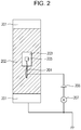
- FIG. 2 is a top view of an electroconductive layer, illustrating a method for measuring the volume resistivity of the electroconductive layer
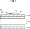
- Fig. 3 is a sectional view of the electroconductive layer, illustrating the method.
- the volume resistivity of the electroconductive layer is measured at normal temperature and normal humidity (temperature: 23°C, relative humidity: 50%).
- a copper tape 203 (product code No. 1181, manufactured by 3M) is stuck to the surface of the electroconductive layer 202. This tape is used as the front side electrode of the electroconductive layer 202.
- the support member 201 is used as the rear side electrode of the electroconductive layer 202.
- a power supply 206 from which a voltage is applied between the copper tape 203 and the support member 201 and a current measuring device 207 for measuring the current flowing between the copper tape 203 and the support member 201 are provided.
- a copper wire 204 is put on the copper tape 203 and fixed so as not to come off from the copper tape 203 by sticking another copper tape 205 onto the copper tape 203.
- a voltage is applied to the copper tape 203 through the copper wire 204.
- the current measuring device 207 used for this measurement is beneficially capable of measuring very small current.
- a current as small as 1 ⁇ 10 -6 A or less in terms of absolute value is measured.
- Such a current measuring device may be, for example, pA meter 4140B manufactured by Hewlett-Packard.
- the volume resistivity of the electroconductive layer may be measured in a state where only the electroconductive layer is formed on the support member, or in a state where only the electroconductive layer is left after the overlying layers (including the photosensitive layer) have been removed from the electrophotographic photosensitive member. Either case obtains the same measurement value.
- An undercoat layer may be disposed on the support member or the electroconductive layer.
- the undercoat layer enhances the adhesion between layers and blocks charge carrier injection.
- Examples of the polymerizable functional group of the monomer include an isocyanate group, blocked isocyanate groups, a methylol group, alkylated methylol groups, and an epoxy group, metal alkoxide groups, a hydroxyl group, an amino group, a carboxy group, a thiol group, a carboxy anhydride group, and a carbon-carbon double bond.
- the undercoat layer may further contain an electron transporting material, a metal oxide, a metal, or an electrically conductive polymer from the viewpoint of increasing the electrical properties thereof.
- an electron transporting material or a metal oxide may be added.
- the electron transporting material examples include quinone compounds, imide compounds, benzimidazole compounds, cyclopentadienylidene compounds, fluorenone compounds, xanthone compounds, benzophenone compounds, cyanovinyl compounds, halogenated aryl compounds, silole compounds, and boron-containing compounds.
- the undercoat layer may be a cured film formed by polymerizing an electron transporting material having a polymerizable functional group with any of the above-cited monomers having a polymerizable functional group.
- Examples of the resin contained in the charge generating layer include polyester resin, polycarbonate resin, polyvinyl acetal resin, polyvinyl butyral resin, acrylic resin, silicone resin, epoxy resin, melamine resin, polyurethane resin, phenol resin, polyvinyl alcohol resin, cellulose resin, polystyrene resin, polyvinyl acetate resin, and polyvinyl chloride resin.
- polyester resin polycarbonate resin
- polyvinyl acetal resin polyvinyl butyral resin
- acrylic resin silicone resin
- epoxy resin epoxy resin
- melamine resin polyurethane resin
- phenol resin polyvinyl alcohol resin
- cellulose resin cellulose resin
- polystyrene resin polyvinyl acetate resin
- polyvinyl chloride resin polyvinyl chloride resin
- the thickness of the charge generating layer may be in the range of 0.1 ⁇ m to 1 ⁇ m, such as in the range of 0.15 ⁇ m to 0.4 ⁇ m.
- the average thickness of the charge transport layer may be in the range of 5 ⁇ m to 50 ⁇ m, such as 8 ⁇ m to 40 ⁇ m or 10 ⁇ m to 30 ⁇ m.
- Examples of the charge transporting material include polycyclic aromatic compounds, heterocyclic compounds, hydrazone compounds, styryl compounds, enamine compounds, benzidine compounds, triarylamine compounds, and resins having a group derived from these compounds. Triarylamine compounds and benzidine compounds are beneficial.
- the protective layer may be a cured film formed by polymerizing a composition containing a monomer having a polymerizable functional group.
- a thermal polymerization reaction, a photopolymerization reaction, a radiation polymerization reaction, or the like may be conducted.
- the polymerizable functional group of the monomer may be an acryloyl group or a methacryloyl group.
- the monomer having a polymerizable functional group may have a charge transporting function.
- the protective layer may further contain an antioxidant, a UV absorbent, a plasticizer, a leveling agent, a lubricant, an abrasion resistance improver, and any other additive. More specifically, examples of such an additive include hindered phenol compounds, hindered amine compounds, sulfur compounds, phosphorus compounds, benzophenone compounds, siloxane-modified resin, silicone oil, fluororesin particles, polystyrene resin particles, polyethylene resin particles, silica particles, alumina particles, and boron nitride particles.
- an additive include hindered phenol compounds, hindered amine compounds, sulfur compounds, phosphorus compounds, benzophenone compounds, siloxane-modified resin, silicone oil, fluororesin particles, polystyrene resin particles, polyethylene resin particles, silica particles, alumina particles, and boron nitride particles.
- the thickness of the protective layer may be in the range of 0.5 ⁇ m to 10 ⁇ m, such as in the range of 1 ⁇ m to 7 ⁇ m.
- the protective layer may be formed by applying a coating liquid containing the above-described ingredients and a solvent to form a coating film, followed by drying and/or curing.
- the solvent of the coating liquid for the protective layer may be an alcohol-based solvent, a ketone-based solvent, an ether-based solvent, a sulfoxide-based solvent, an ester-based solvent, or an aromatic hydrocarbon.
- the electrophotographic apparatus may include a static elimination mechanism operable to remove static electricity from the surface of the electrophotographic photosensitive member 1 with pre-exposure light 10 from a pre-exposure device (not shown). Also, the electrophotographic apparatus may have a guide 12, such as a rail, that guides the removal or attachment of the process cartridge.
- a strontium chloride aqueous solution (0.719 mol in terms of SrO) was added in a SrO/TiO 2 mole ratio of 1.15, followed by adjusting the TiO 2 concentration to 0.313 mol/L. Subsequently, the mixture was heated to 90°C with stirring, and 296 mL of 5 mol/L sodium hydroxide aqueous solution was added to the mixture over a period of 18 hours, followed by stirring at 95°C for 1 hour to complete the reaction. The resulting slurry was cooled to 50°C, and hydrochloric acid was added to the slurry until the pH of the slurry reached 5.0, followed by stirring for 1 hour.
- the resulting precipitate was subjected to decantation and rinsing and was then separated out by filtration.
- the separated precipitate was dried in air at 120°C for 8 hours to yield SrTiO 3 particle powder ST-1.
- the average particle size of the powder measured by electron microscopy was 100 nm, and X-ray diffraction of the powder showed a strontium titanate single phase.
- Carbon black was thus attached to the surfaces of methyl hydrogen polysiloxane-coated SrTiO 3 particles.
- the resulting particles were dried at 80°C for 60 minutes with a dryer to yield carbon black-coated SrTiO 3 particles A-1.
- the stirring speed at this time was 22 rpm.
- electrically conductive composite particles had a volume average particle size of 110 nm and a powder resistivity of 1.1 ⁇ 10 2 ⁇ cm.
- Carbon black-coated BaTiO 3 Particles BT-1 were prepared in the same manner as carbon black-coated SrTiO 3 particles A-1 except that strontium titanate particles ST-1 were replaced with barium titanate particle powder (produced by KCM Corporation, average particle size: 150 nm) .
- Carbon black-coated BaTiO 3 Particles BT-1X were prepared in the same manner as carbon black-coated SrTiO 3 particles A-1 except that strontium titanate particles ST-1 were replaced with barium titanate particle powder (produced by KCM Corporation, average particle size: 300 nm) .
- NaTaO 3 particles TA-1 were prepared as below.
- a high-temperature high-pressure batch type reactor including a Teflon inner cylinder (inner capacity: 50 cm 3 ) was charged with 0.0905 mol/kg Ta 2 O 5 and 7 mol/kg sodium hydroxide.
- the reactor was heated to 145°C in a heater, and the contents in the reactor were subjected to a hydrothermal reaction for 4 hours. After a predetermined time had elapsed, the reaction was stopped by cooling the reactor in a cold bath, and the reaction product was filtered through a simple filter and then dried at 100°C for 30 minutes to yield NaTaO 3 particles TA-1 having an average particle size of 300 nm.
- Carbon black-coated NaTaO 3 particles NT-1 were prepared in the same manner as carbon black-coated SrTiO 3 particles A-1 except that NaTaO 3 particles TA-1 were coated with carbon black.
- Carbon black-coated BaZrO 3 Particles BZ-1 were prepared in the same manner as carbon black-coated SrTiO 3 particles A-1 except that strontium titanate particles ST-1 were replaced with barium zirconate particle powder (produced by Nippon Chemical Industrial, average particle size: 300 nm).
- Ta-doped titanium oxide-coated SrTiO 3 particles A-11 were prepared in the same manner as Nb-doped titanium oxide-coated SrTiO 3 particles A-10 except that niobium pentachloride was replaced with tantalum pentachloride.
- Nb-doped titanium oxide-coated BaTiO 3 particles BT-10 were prepared in the same manner as Nb-doped titanium oxide-coated SrTiO 3 particles A-10 except that strontium titanate particles ST-1 were replaced with barium titanate particle powder (produced by KCM Corporation, average particle size: 150 nm).
- Ta-Doped Titanium Oxide-Coated BaTiO 3 Particles BT-11
- a 10 nm-thick copper coating film was formed over the surfaces of strontium titanate particles ST-1 by electroless plating to yield copper-coated strontium titanate particles A-2.
- a 10 nm-thick silver coating film was formed over the surfaces of strontium titanate particles ST-1 by electroless plating to yield silver-coated strontium titanate particles A-3.
- the glass beads were removed from the resulting dispersion liquid by using a mesh. Then, 0.01 part of silicone oil SH28 PAINT ADDITIVE (produced by Dow Corning Toray) as a leveling agent and 3 parts of crosslinked polymethyl methacrylate (PMMA) particles Techpolymer SSX-102 (produced by Sekisui Plastics, average primary particle size: 2.5 ⁇ m) as a surface roughness agent were added into the dispersion liquid, and the mixture was stirred to yield electroconductive layer-forming coating liquid 1.
- silicone oil SH28 PAINT ADDITIVE produced by Dow Corning Toray
- PMMA polymethyl methacrylate
- Techpolymer SSX-102 produced by Sekisui Plastics, average primary particle size: 2.5 ⁇ m
- Electroconductive layer-forming coating liquid 32 was prepared in the same manner as electroconductive layer-forming coating liquid 28 except that P-doped tin oxide-coated barium titanate particles BT-5 were replaced with Nb-doped titanium oxide-coated BaTiO 3 particles BT-10. Preparation of Electrophotographic Photosensitive Members Electrophotographic Photosensitive Member 1
Landscapes
- Physics & Mathematics (AREA)
- General Physics & Mathematics (AREA)
- Chemical & Material Sciences (AREA)
- Inorganic Chemistry (AREA)
- Photoreceptors In Electrophotography (AREA)
Applications Claiming Priority (1)
| Application Number | Priority Date | Filing Date | Title |
|---|---|---|---|
| JP2017037739 | 2017-02-28 |
Publications (2)
| Publication Number | Publication Date |
|---|---|
| EP3367168A1 EP3367168A1 (en) | 2018-08-29 |
| EP3367168B1 true EP3367168B1 (en) | 2020-06-24 |
Family
ID=61283053
Family Applications (1)
| Application Number | Title | Priority Date | Filing Date |
|---|---|---|---|
| EP18158550.6A Active EP3367168B1 (en) | 2017-02-28 | 2018-02-26 | Electrophotographic photosensitive member, process cartridge, and electrophotographic apparatus |
Country Status (4)
| Country | Link |
|---|---|
| US (1) | US10216105B2 (enExample) |
| EP (1) | EP3367168B1 (enExample) |
| JP (1) | JP7034760B2 (enExample) |
| CN (1) | CN108508716B (enExample) |
Families Citing this family (10)
| Publication number | Priority date | Publication date | Assignee | Title |
|---|---|---|---|---|
| JP6918663B2 (ja) * | 2017-09-26 | 2021-08-11 | キヤノン株式会社 | 電子写真感光体、プロセスカートリッジおよび電子写真装置 |
| JP7330807B2 (ja) * | 2018-08-24 | 2023-08-22 | キヤノン株式会社 | 電子写真感光体、プロセスカートリッジ及び電子写真装置 |
| US10948838B2 (en) * | 2018-08-24 | 2021-03-16 | Canon Kabushiki Kaisha | Electrophotographic photosensitive member, process cartridge and electrophotographic apparatus |
| JP2020060748A (ja) * | 2018-10-12 | 2020-04-16 | キヤノン株式会社 | 電子写真感光体、プロセスカートリッジおよび電子写真装置 |
| JP7267710B2 (ja) * | 2018-10-17 | 2023-05-02 | キヤノン株式会社 | 電子写真感光体、プロセスカートリッジ及び電子写真装置 |
| JP7204419B2 (ja) * | 2018-10-24 | 2023-01-16 | キヤノン株式会社 | 電子写真感光体、プロセスカートリッジ及び電子写真装置 |
| JP7187266B2 (ja) | 2018-10-25 | 2022-12-12 | キヤノン株式会社 | 電子写真感光体、プロセスカートリッジ及び電子写真装置 |
| JP7175713B2 (ja) * | 2018-10-25 | 2022-11-21 | キヤノン株式会社 | 電子写真感光体、プロセスカートリッジ及び電子写真装置 |
| JP7314550B2 (ja) | 2019-03-20 | 2023-07-26 | 富士フイルムビジネスイノベーション株式会社 | 電子写真感光体、プロセスカートリッジ及び画像形成装置 |
| JP7475941B2 (ja) | 2020-04-13 | 2024-04-30 | キヤノン株式会社 | 電子写真感光体、プロセスカートリッジ及び電子写真装置 |
Family Cites Families (27)
| Publication number | Priority date | Publication date | Assignee | Title |
|---|---|---|---|---|
| US4579801A (en) | 1983-08-02 | 1986-04-01 | Canon Kabushiki Kaisha | Electrophotographic photosensitive member having phenolic subbing layer |
| JPS63180964A (ja) * | 1987-01-21 | 1988-07-26 | Ricoh Co Ltd | 電子写真感光体 |
| JP2879084B2 (ja) | 1990-03-30 | 1999-04-05 | 株式会社リコー | 電子写真感光体 |
| JPH04134352A (ja) * | 1990-05-16 | 1992-05-08 | Tomoegawa Paper Co Ltd | 導電性支持体及びそれを使用した記録体 |
| JPH0746235B2 (ja) * | 1990-06-04 | 1995-05-17 | 株式会社巴川製紙所 | 導電性支持体 |
| JP3083047B2 (ja) * | 1993-06-30 | 2000-09-04 | キヤノン株式会社 | 電子写真感光体、該電子写真感光体を有するプロセスカートリッジ及び電子写真装置 |
| US5486440A (en) * | 1993-06-30 | 1996-01-23 | Canon Kabushiki Kaisha | Electrophotographic photosensitive member, and process cartridge and electrophotographic apparatus employing the same |
| JPH07234533A (ja) * | 1994-02-23 | 1995-09-05 | New Oji Paper Co Ltd | 電子写真平版印刷版材料 |
| JPH07239575A (ja) * | 1994-02-28 | 1995-09-12 | New Oji Paper Co Ltd | 電子写真平版印刷版材料 |
| EP0838729B1 (en) | 1996-10-23 | 2003-05-21 | Mitsubishi Chemical Corporation | Electrophotographic copying method and electrophotographic copying machine used in the method |
| JPH11109669A (ja) | 1997-10-01 | 1999-04-23 | Canon Inc | 電子写真感光体およびそれを用いた電子写真装置 |
| JP4075584B2 (ja) | 2002-11-25 | 2008-04-16 | コニカミノルタホールディングス株式会社 | 画像形成方法及び画像形成装置 |
| JP3988685B2 (ja) | 2003-06-24 | 2007-10-10 | コニカミノルタビジネステクノロジーズ株式会社 | 電子写真感光体、プロセスカートリッジ、画像形成装置及び画像形成方法 |
| JP2005242155A (ja) | 2004-02-27 | 2005-09-08 | Canon Inc | 電子写真感光体及びそれを用いる電子写真プロセスカートリッジ、及び電子写真装置 |
| JP5194552B2 (ja) | 2006-05-18 | 2013-05-08 | 三菱化学株式会社 | 電子写真感光体の下引き層形成用塗布液 |
| JP5301370B2 (ja) | 2008-07-02 | 2013-09-25 | 石原産業株式会社 | 酸化スズ粒子及びその製造方法 |
| JP2010091796A (ja) | 2008-10-08 | 2010-04-22 | Canon Inc | 電子写真装置 |
| JP2010170015A (ja) * | 2009-01-26 | 2010-08-05 | Konica Minolta Business Technologies Inc | 感光層の表面研磨方法 |
| JP4956654B2 (ja) * | 2009-09-04 | 2012-06-20 | キヤノン株式会社 | 電子写真感光体、プロセスカートリッジ、電子写真装置および電子写真感光体の製造方法 |
| JP5543412B2 (ja) | 2009-09-04 | 2014-07-09 | キヤノン株式会社 | 電子写真感光体、プロセスカートリッジおよび電子写真装置 |
| JP5361666B2 (ja) | 2009-11-02 | 2013-12-04 | キヤノン株式会社 | 電子写真感光体、プロセスカートリッジおよび電子写真装置 |
| JP4764953B1 (ja) * | 2009-12-09 | 2011-09-07 | キヤノン株式会社 | 電子写真感光体、プロセスカートリッジおよび電子写真装置 |
| JP2014016609A (ja) * | 2012-06-14 | 2014-01-30 | Mitsubishi Chemicals Corp | 画像形成装置および電子写真感光体 |
| JP6074295B2 (ja) | 2012-08-30 | 2017-02-01 | キヤノン株式会社 | 電子写真感光体、プロセスカートリッジおよび電子写真装置、ならびに、電子写真感光体の製造方法 |
| JP6061761B2 (ja) | 2012-08-30 | 2017-01-18 | キヤノン株式会社 | 電子写真感光体、プロセスカートリッジおよび電子写真装置 |
| JP5990154B2 (ja) * | 2013-10-30 | 2016-09-07 | 京セラドキュメントソリューションズ株式会社 | 積層型電子写真感光体 |
| CN105867080B (zh) | 2015-02-09 | 2019-10-11 | 佳能株式会社 | 电子照相感光构件、处理盒和电子照相设备 |
-
2018
- 2018-02-23 JP JP2018031125A patent/JP7034760B2/ja active Active
- 2018-02-23 US US15/903,802 patent/US10216105B2/en active Active
- 2018-02-26 EP EP18158550.6A patent/EP3367168B1/en active Active
- 2018-02-27 CN CN201810164024.9A patent/CN108508716B/zh active Active
Non-Patent Citations (1)
| Title |
|---|
| None * |
Also Published As
| Publication number | Publication date |
|---|---|
| CN108508716B (zh) | 2021-12-21 |
| JP2018141972A (ja) | 2018-09-13 |
| US10216105B2 (en) | 2019-02-26 |
| CN108508716A (zh) | 2018-09-07 |
| JP7034760B2 (ja) | 2022-03-14 |
| US20180246427A1 (en) | 2018-08-30 |
| EP3367168A1 (en) | 2018-08-29 |
Similar Documents
| Publication | Publication Date | Title |
|---|---|---|
| EP3367168B1 (en) | Electrophotographic photosensitive member, process cartridge, and electrophotographic apparatus | |
| US10942462B2 (en) | Electrophotographic photosensitive member, process cartridge, and electrophotographic apparatus | |
| EP3367167B1 (en) | Electrophotographic photosensitive member, process cartridge, and electrophotographic apparatus | |
| EP2422240B1 (en) | Electrophotographic photosensitive member, process cartridge, and electrophotographic apparatus | |
| EP2816412B1 (en) | Process for producing electrophotographic photosensitive member | |
| EP3367169B1 (en) | Electrophotographic photosensitive member, process cartridge and electrophotographic apparatus | |
| CN101878453B (zh) | 电子照相感光构件、生产电子照相感光构件的方法、处理盒和电子照相设备 | |
| EP2703890B1 (en) | Electrophotographic photosensitive member, process cartridge and electrophotographic apparatus, and method for producing electrophotographic photosensitive member | |
| EP2422241B1 (en) | Electrophotographic photosensitive member, method for producing electrophotographic photosensitive member, process cartridge, and electrophotographic apparatus | |
| EP3534215A1 (en) | Electrophotographic photosensitive member, process cartridge, and electrophotographic apparatus | |
| EP1521126B1 (en) | Electrophotographic photoreceptor, method for manufacturing the electrophotographic photoreceptor, and image forming apparatus and process cartridge using the electrophotographic photoreceptor | |
| US11169453B2 (en) | Electrophotographic photosensitive member, process cartridge and electrophotographic apparatus | |
| JP6643124B2 (ja) | 電子写真感光体、プロセスカートリッジおよび電子写真装置 | |
| KR20120045061A (ko) | 전자 사진 감광체, 프로세스 카트리지 및 전자 사진 장치 | |
| DE102018110055A1 (de) | Elektrofotografisches lichtempfindliches Element, Prozesskartusche und elektrofotografisches Gerät | |
| JP7739082B2 (ja) | 電子写真感光体、プロセスカートリッジ及び電子写真装置 | |
| JP7114403B2 (ja) | 電子写真感光体の製造方法 | |
| CN109976113B (zh) | 电子照相感光构件、处理盒和电子照相设备 | |
| JP3917087B2 (ja) | 分散液の作製方法、電子写真感光体、画像形成装置および画像形成装置用プロセスカートリッジ | |
| JP3834003B2 (ja) | 分散液の作製方法、電子写真感光体、画像形成装置及び画像形成装置用プロセスカートリッジ | |
| JP3917082B2 (ja) | 分散液の作製方法、電子写真感光体、画像形成装置及び画像形成装置用プロセスカートリッジ | |
| EP4557006A1 (en) | Electrophotographic photosensitive member, process cartridge, and electrophotographic apparatus | |
| JP3948730B2 (ja) | 電子写真感光体、電子写真感光体の製造方法、及び電子写真装置 | |
| JP2002148826A (ja) | 電子写真感光体、電子写真感光体用塗布液およびその製造方法、これを用いた画像形成装置 |
Legal Events
| Date | Code | Title | Description |
|---|---|---|---|
| PUAI | Public reference made under article 153(3) epc to a published international application that has entered the european phase |
Free format text: ORIGINAL CODE: 0009012 |
|
| STAA | Information on the status of an ep patent application or granted ep patent |
Free format text: STATUS: THE APPLICATION HAS BEEN PUBLISHED |
|
| AK | Designated contracting states |
Kind code of ref document: A1 Designated state(s): AL AT BE BG CH CY CZ DE DK EE ES FI FR GB GR HR HU IE IS IT LI LT LU LV MC MK MT NL NO PL PT RO RS SE SI SK SM TR |
|
| AX | Request for extension of the european patent |
Extension state: BA ME |
|
| STAA | Information on the status of an ep patent application or granted ep patent |
Free format text: STATUS: REQUEST FOR EXAMINATION WAS MADE |
|
| 17P | Request for examination filed |
Effective date: 20190228 |
|
| RBV | Designated contracting states (corrected) |
Designated state(s): AL AT BE BG CH CY CZ DE DK EE ES FI FR GB GR HR HU IE IS IT LI LT LU LV MC MK MT NL NO PL PT RO RS SE SI SK SM TR |
|
| GRAP | Despatch of communication of intention to grant a patent |
Free format text: ORIGINAL CODE: EPIDOSNIGR1 |
|
| STAA | Information on the status of an ep patent application or granted ep patent |
Free format text: STATUS: GRANT OF PATENT IS INTENDED |
|
| INTG | Intention to grant announced |
Effective date: 20200214 |
|
| GRAS | Grant fee paid |
Free format text: ORIGINAL CODE: EPIDOSNIGR3 |
|
| GRAA | (expected) grant |
Free format text: ORIGINAL CODE: 0009210 |
|
| STAA | Information on the status of an ep patent application or granted ep patent |
Free format text: STATUS: THE PATENT HAS BEEN GRANTED |
|
| AK | Designated contracting states |
Kind code of ref document: B1 Designated state(s): AL AT BE BG CH CY CZ DE DK EE ES FI FR GB GR HR HU IE IS IT LI LT LU LV MC MK MT NL NO PL PT RO RS SE SI SK SM TR |
|
| REG | Reference to a national code |
Ref country code: GB Ref legal event code: FG4D |
|
| REG | Reference to a national code |
Ref country code: CH Ref legal event code: EP |
|
| REG | Reference to a national code |
Ref country code: DE Ref legal event code: R096 Ref document number: 602018005452 Country of ref document: DE |
|
| REG | Reference to a national code |
Ref country code: AT Ref legal event code: REF Ref document number: 1284493 Country of ref document: AT Kind code of ref document: T Effective date: 20200715 |
|
| REG | Reference to a national code |
Ref country code: IE Ref legal event code: FG4D |
|
| PG25 | Lapsed in a contracting state [announced via postgrant information from national office to epo] |
Ref country code: GR Free format text: LAPSE BECAUSE OF FAILURE TO SUBMIT A TRANSLATION OF THE DESCRIPTION OR TO PAY THE FEE WITHIN THE PRESCRIBED TIME-LIMIT Effective date: 20200925 Ref country code: FI Free format text: LAPSE BECAUSE OF FAILURE TO SUBMIT A TRANSLATION OF THE DESCRIPTION OR TO PAY THE FEE WITHIN THE PRESCRIBED TIME-LIMIT Effective date: 20200624 Ref country code: SE Free format text: LAPSE BECAUSE OF FAILURE TO SUBMIT A TRANSLATION OF THE DESCRIPTION OR TO PAY THE FEE WITHIN THE PRESCRIBED TIME-LIMIT Effective date: 20200624 Ref country code: NO Free format text: LAPSE BECAUSE OF FAILURE TO SUBMIT A TRANSLATION OF THE DESCRIPTION OR TO PAY THE FEE WITHIN THE PRESCRIBED TIME-LIMIT Effective date: 20200924 Ref country code: LT Free format text: LAPSE BECAUSE OF FAILURE TO SUBMIT A TRANSLATION OF THE DESCRIPTION OR TO PAY THE FEE WITHIN THE PRESCRIBED TIME-LIMIT Effective date: 20200624 |
|
| REG | Reference to a national code |
Ref country code: LT Ref legal event code: MG4D |
|
| PG25 | Lapsed in a contracting state [announced via postgrant information from national office to epo] |
Ref country code: BG Free format text: LAPSE BECAUSE OF FAILURE TO SUBMIT A TRANSLATION OF THE DESCRIPTION OR TO PAY THE FEE WITHIN THE PRESCRIBED TIME-LIMIT Effective date: 20200924 Ref country code: LV Free format text: LAPSE BECAUSE OF FAILURE TO SUBMIT A TRANSLATION OF THE DESCRIPTION OR TO PAY THE FEE WITHIN THE PRESCRIBED TIME-LIMIT Effective date: 20200624 Ref country code: HR Free format text: LAPSE BECAUSE OF FAILURE TO SUBMIT A TRANSLATION OF THE DESCRIPTION OR TO PAY THE FEE WITHIN THE PRESCRIBED TIME-LIMIT Effective date: 20200624 Ref country code: RS Free format text: LAPSE BECAUSE OF FAILURE TO SUBMIT A TRANSLATION OF THE DESCRIPTION OR TO PAY THE FEE WITHIN THE PRESCRIBED TIME-LIMIT Effective date: 20200624 |
|
| REG | Reference to a national code |
Ref country code: NL Ref legal event code: MP Effective date: 20200624 |
|
| REG | Reference to a national code |
Ref country code: AT Ref legal event code: MK05 Ref document number: 1284493 Country of ref document: AT Kind code of ref document: T Effective date: 20200624 |
|
| PG25 | Lapsed in a contracting state [announced via postgrant information from national office to epo] |
Ref country code: AL Free format text: LAPSE BECAUSE OF FAILURE TO SUBMIT A TRANSLATION OF THE DESCRIPTION OR TO PAY THE FEE WITHIN THE PRESCRIBED TIME-LIMIT Effective date: 20200624 Ref country code: NL Free format text: LAPSE BECAUSE OF FAILURE TO SUBMIT A TRANSLATION OF THE DESCRIPTION OR TO PAY THE FEE WITHIN THE PRESCRIBED TIME-LIMIT Effective date: 20200624 |
|
| PG25 | Lapsed in a contracting state [announced via postgrant information from national office to epo] |
Ref country code: PT Free format text: LAPSE BECAUSE OF FAILURE TO SUBMIT A TRANSLATION OF THE DESCRIPTION OR TO PAY THE FEE WITHIN THE PRESCRIBED TIME-LIMIT Effective date: 20201026 Ref country code: ES Free format text: LAPSE BECAUSE OF FAILURE TO SUBMIT A TRANSLATION OF THE DESCRIPTION OR TO PAY THE FEE WITHIN THE PRESCRIBED TIME-LIMIT Effective date: 20200624 Ref country code: EE Free format text: LAPSE BECAUSE OF FAILURE TO SUBMIT A TRANSLATION OF THE DESCRIPTION OR TO PAY THE FEE WITHIN THE PRESCRIBED TIME-LIMIT Effective date: 20200624 Ref country code: AT Free format text: LAPSE BECAUSE OF FAILURE TO SUBMIT A TRANSLATION OF THE DESCRIPTION OR TO PAY THE FEE WITHIN THE PRESCRIBED TIME-LIMIT Effective date: 20200624 Ref country code: IT Free format text: LAPSE BECAUSE OF FAILURE TO SUBMIT A TRANSLATION OF THE DESCRIPTION OR TO PAY THE FEE WITHIN THE PRESCRIBED TIME-LIMIT Effective date: 20200624 Ref country code: SM Free format text: LAPSE BECAUSE OF FAILURE TO SUBMIT A TRANSLATION OF THE DESCRIPTION OR TO PAY THE FEE WITHIN THE PRESCRIBED TIME-LIMIT Effective date: 20200624 Ref country code: CZ Free format text: LAPSE BECAUSE OF FAILURE TO SUBMIT A TRANSLATION OF THE DESCRIPTION OR TO PAY THE FEE WITHIN THE PRESCRIBED TIME-LIMIT Effective date: 20200624 Ref country code: RO Free format text: LAPSE BECAUSE OF FAILURE TO SUBMIT A TRANSLATION OF THE DESCRIPTION OR TO PAY THE FEE WITHIN THE PRESCRIBED TIME-LIMIT Effective date: 20200624 |
|
| PG25 | Lapsed in a contracting state [announced via postgrant information from national office to epo] |
Ref country code: IS Free format text: LAPSE BECAUSE OF FAILURE TO SUBMIT A TRANSLATION OF THE DESCRIPTION OR TO PAY THE FEE WITHIN THE PRESCRIBED TIME-LIMIT Effective date: 20201024 Ref country code: PL Free format text: LAPSE BECAUSE OF FAILURE TO SUBMIT A TRANSLATION OF THE DESCRIPTION OR TO PAY THE FEE WITHIN THE PRESCRIBED TIME-LIMIT Effective date: 20200624 Ref country code: SK Free format text: LAPSE BECAUSE OF FAILURE TO SUBMIT A TRANSLATION OF THE DESCRIPTION OR TO PAY THE FEE WITHIN THE PRESCRIBED TIME-LIMIT Effective date: 20200624 |
|
| REG | Reference to a national code |
Ref country code: DE Ref legal event code: R097 Ref document number: 602018005452 Country of ref document: DE |
|
| PG25 | Lapsed in a contracting state [announced via postgrant information from national office to epo] |
Ref country code: DK Free format text: LAPSE BECAUSE OF FAILURE TO SUBMIT A TRANSLATION OF THE DESCRIPTION OR TO PAY THE FEE WITHIN THE PRESCRIBED TIME-LIMIT Effective date: 20200624 |
|
| PLBE | No opposition filed within time limit |
Free format text: ORIGINAL CODE: 0009261 |
|
| STAA | Information on the status of an ep patent application or granted ep patent |
Free format text: STATUS: NO OPPOSITION FILED WITHIN TIME LIMIT |
|
| 26N | No opposition filed |
Effective date: 20210325 |
|
| PG25 | Lapsed in a contracting state [announced via postgrant information from national office to epo] |
Ref country code: SI Free format text: LAPSE BECAUSE OF FAILURE TO SUBMIT A TRANSLATION OF THE DESCRIPTION OR TO PAY THE FEE WITHIN THE PRESCRIBED TIME-LIMIT Effective date: 20200624 |
|
| PG25 | Lapsed in a contracting state [announced via postgrant information from national office to epo] |
Ref country code: MC Free format text: LAPSE BECAUSE OF FAILURE TO SUBMIT A TRANSLATION OF THE DESCRIPTION OR TO PAY THE FEE WITHIN THE PRESCRIBED TIME-LIMIT Effective date: 20200624 |
|
| REG | Reference to a national code |
Ref country code: BE Ref legal event code: MM Effective date: 20210228 |
|
| PG25 | Lapsed in a contracting state [announced via postgrant information from national office to epo] |
Ref country code: CH Free format text: LAPSE BECAUSE OF NON-PAYMENT OF DUE FEES Effective date: 20210228 Ref country code: LU Free format text: LAPSE BECAUSE OF NON-PAYMENT OF DUE FEES Effective date: 20210226 Ref country code: LI Free format text: LAPSE BECAUSE OF NON-PAYMENT OF DUE FEES Effective date: 20210228 |
|
| PG25 | Lapsed in a contracting state [announced via postgrant information from national office to epo] |
Ref country code: FR Free format text: LAPSE BECAUSE OF NON-PAYMENT OF DUE FEES Effective date: 20210228 Ref country code: IE Free format text: LAPSE BECAUSE OF NON-PAYMENT OF DUE FEES Effective date: 20210226 |
|
| PG25 | Lapsed in a contracting state [announced via postgrant information from national office to epo] |
Ref country code: BE Free format text: LAPSE BECAUSE OF NON-PAYMENT OF DUE FEES Effective date: 20210228 |
|
| GBPC | Gb: european patent ceased through non-payment of renewal fee |
Effective date: 20220226 |
|
| PG25 | Lapsed in a contracting state [announced via postgrant information from national office to epo] |
Ref country code: GB Free format text: LAPSE BECAUSE OF NON-PAYMENT OF DUE FEES Effective date: 20220226 |
|
| PG25 | Lapsed in a contracting state [announced via postgrant information from national office to epo] |
Ref country code: CY Free format text: LAPSE BECAUSE OF FAILURE TO SUBMIT A TRANSLATION OF THE DESCRIPTION OR TO PAY THE FEE WITHIN THE PRESCRIBED TIME-LIMIT Effective date: 20200624 |
|
| PG25 | Lapsed in a contracting state [announced via postgrant information from national office to epo] |
Ref country code: HU Free format text: LAPSE BECAUSE OF FAILURE TO SUBMIT A TRANSLATION OF THE DESCRIPTION OR TO PAY THE FEE WITHIN THE PRESCRIBED TIME-LIMIT; INVALID AB INITIO Effective date: 20180226 |
|
| PG25 | Lapsed in a contracting state [announced via postgrant information from national office to epo] |
Ref country code: MK Free format text: LAPSE BECAUSE OF FAILURE TO SUBMIT A TRANSLATION OF THE DESCRIPTION OR TO PAY THE FEE WITHIN THE PRESCRIBED TIME-LIMIT Effective date: 20200624 |
|
| PG25 | Lapsed in a contracting state [announced via postgrant information from national office to epo] |
Ref country code: MT Free format text: LAPSE BECAUSE OF FAILURE TO SUBMIT A TRANSLATION OF THE DESCRIPTION OR TO PAY THE FEE WITHIN THE PRESCRIBED TIME-LIMIT Effective date: 20200624 |
|
| PG25 | Lapsed in a contracting state [announced via postgrant information from national office to epo] |
Ref country code: TR Free format text: LAPSE BECAUSE OF FAILURE TO SUBMIT A TRANSLATION OF THE DESCRIPTION OR TO PAY THE FEE WITHIN THE PRESCRIBED TIME-LIMIT Effective date: 20200624 |
|
| PGFP | Annual fee paid to national office [announced via postgrant information from national office to epo] |
Ref country code: DE Payment date: 20260121 Year of fee payment: 9 |