EP3358614B1 - Schaltsubstrat und halbleiterbauelement - Google Patents
Schaltsubstrat und halbleiterbauelement Download PDFInfo
- Publication number
- EP3358614B1 EP3358614B1 EP16850544.4A EP16850544A EP3358614B1 EP 3358614 B1 EP3358614 B1 EP 3358614B1 EP 16850544 A EP16850544 A EP 16850544A EP 3358614 B1 EP3358614 B1 EP 3358614B1
- Authority
- EP
- European Patent Office
- Prior art keywords
- metal plate
- less
- circuit substrate
- substrate
- thickness
- Prior art date
- Legal status (The legal status is an assumption and is not a legal conclusion. Google has not performed a legal analysis and makes no representation as to the accuracy of the status listed.)
- Active
Links
Images
Classifications
-
- H—ELECTRICITY
- H10—SEMICONDUCTOR DEVICES; ELECTRIC SOLID-STATE DEVICES NOT OTHERWISE PROVIDED FOR
- H10W—GENERIC PACKAGES, INTERCONNECTIONS, CONNECTORS OR OTHER CONSTRUCTIONAL DETAILS OF DEVICES COVERED BY CLASS H10
- H10W70/00—Package substrates; Interposers; Redistribution layers [RDL]
- H10W70/60—Insulating or insulated package substrates; Interposers; Redistribution layers
- H10W70/67—Insulating or insulated package substrates; Interposers; Redistribution layers characterised by their insulating layers or insulating parts
- H10W70/68—Shapes or dispositions thereof
-
- H—ELECTRICITY
- H10—SEMICONDUCTOR DEVICES; ELECTRIC SOLID-STATE DEVICES NOT OTHERWISE PROVIDED FOR
- H10W—GENERIC PACKAGES, INTERCONNECTIONS, CONNECTORS OR OTHER CONSTRUCTIONAL DETAILS OF DEVICES COVERED BY CLASS H10
- H10W40/00—Arrangements for thermal protection or thermal control
- H10W40/20—Arrangements for cooling
- H10W40/25—Arrangements for cooling characterised by their materials
- H10W40/255—Arrangements for cooling characterised by their materials having a laminate or multilayered structure, e.g. direct bond copper [DBC] ceramic substrates
-
- C—CHEMISTRY; METALLURGY
- C04—CEMENTS; CONCRETE; ARTIFICIAL STONE; CERAMICS; REFRACTORIES
- C04B—LIME, MAGNESIA; SLAG; CEMENTS; COMPOSITIONS THEREOF, e.g. MORTARS, CONCRETE OR LIKE BUILDING MATERIALS; ARTIFICIAL STONE; CERAMICS; REFRACTORIES; TREATMENT OF NATURAL STONE
- C04B37/00—Joining burned ceramic articles with other burned ceramic articles or other articles by heating
- C04B37/02—Joining burned ceramic articles with other burned ceramic articles or other articles by heating with metallic articles
- C04B37/023—Joining burned ceramic articles with other burned ceramic articles or other articles by heating with metallic articles characterised by the interlayer used
- C04B37/026—Joining burned ceramic articles with other burned ceramic articles or other articles by heating with metallic articles characterised by the interlayer used consisting of metals or metal salts
-
- H—ELECTRICITY
- H05—ELECTRIC TECHNIQUES NOT OTHERWISE PROVIDED FOR
- H05K—PRINTED CIRCUITS; CASINGS OR CONSTRUCTIONAL DETAILS OF ELECTRIC APPARATUS; MANUFACTURE OF ASSEMBLAGES OF ELECTRICAL COMPONENTS
- H05K1/00—Printed circuits
- H05K1/02—Details
-
- H—ELECTRICITY
- H05—ELECTRIC TECHNIQUES NOT OTHERWISE PROVIDED FOR
- H05K—PRINTED CIRCUITS; CASINGS OR CONSTRUCTIONAL DETAILS OF ELECTRIC APPARATUS; MANUFACTURE OF ASSEMBLAGES OF ELECTRICAL COMPONENTS
- H05K1/00—Printed circuits
- H05K1/02—Details
- H05K1/0213—Electrical arrangements not otherwise provided for
- H05K1/0263—High current adaptations, e.g. printed high current conductors or using auxiliary non-printed means; Fine and coarse circuit patterns on one circuit board
- H05K1/0265—High current adaptations, e.g. printed high current conductors or using auxiliary non-printed means; Fine and coarse circuit patterns on one circuit board characterized by the lay-out of or details of the printed conductors, e.g. reinforced conductors, redundant conductors, conductors having different cross-sections
-
- H—ELECTRICITY
- H05—ELECTRIC TECHNIQUES NOT OTHERWISE PROVIDED FOR
- H05K—PRINTED CIRCUITS; CASINGS OR CONSTRUCTIONAL DETAILS OF ELECTRIC APPARATUS; MANUFACTURE OF ASSEMBLAGES OF ELECTRICAL COMPONENTS
- H05K1/00—Printed circuits
- H05K1/02—Details
- H05K1/0271—Arrangements for reducing stress or warp in rigid printed circuit boards, e.g. caused by loads, vibrations or differences in thermal expansion
-
- H—ELECTRICITY
- H05—ELECTRIC TECHNIQUES NOT OTHERWISE PROVIDED FOR
- H05K—PRINTED CIRCUITS; CASINGS OR CONSTRUCTIONAL DETAILS OF ELECTRIC APPARATUS; MANUFACTURE OF ASSEMBLAGES OF ELECTRICAL COMPONENTS
- H05K1/00—Printed circuits
- H05K1/02—Details
- H05K1/03—Use of materials for the substrate
- H05K1/0306—Inorganic insulating substrates, e.g. ceramic, glass
-
- H—ELECTRICITY
- H05—ELECTRIC TECHNIQUES NOT OTHERWISE PROVIDED FOR
- H05K—PRINTED CIRCUITS; CASINGS OR CONSTRUCTIONAL DETAILS OF ELECTRIC APPARATUS; MANUFACTURE OF ASSEMBLAGES OF ELECTRICAL COMPONENTS
- H05K3/00—Apparatus or processes for manufacturing printed circuits
- H05K3/38—Improvement of the adhesion between the insulating substrate and the metal
- H05K3/388—Improvement of the adhesion between the insulating substrate and the metal by the use of a metallic or inorganic thin film adhesion layer
-
- H—ELECTRICITY
- H10—SEMICONDUCTOR DEVICES; ELECTRIC SOLID-STATE DEVICES NOT OTHERWISE PROVIDED FOR
- H10W—GENERIC PACKAGES, INTERCONNECTIONS, CONNECTORS OR OTHER CONSTRUCTIONAL DETAILS OF DEVICES COVERED BY CLASS H10
- H10W70/00—Package substrates; Interposers; Redistribution layers [RDL]
- H10W70/60—Insulating or insulated package substrates; Interposers; Redistribution layers
- H10W70/67—Insulating or insulated package substrates; Interposers; Redistribution layers characterised by their insulating layers or insulating parts
- H10W70/68—Shapes or dispositions thereof
- H10W70/6875—Shapes or dispositions thereof being on a metallic substrate, e.g. insulated metal substrates [IMS]
-
- H—ELECTRICITY
- H10—SEMICONDUCTOR DEVICES; ELECTRIC SOLID-STATE DEVICES NOT OTHERWISE PROVIDED FOR
- H10W—GENERIC PACKAGES, INTERCONNECTIONS, CONNECTORS OR OTHER CONSTRUCTIONAL DETAILS OF DEVICES COVERED BY CLASS H10
- H10W70/00—Package substrates; Interposers; Redistribution layers [RDL]
- H10W70/60—Insulating or insulated package substrates; Interposers; Redistribution layers
- H10W70/67—Insulating or insulated package substrates; Interposers; Redistribution layers characterised by their insulating layers or insulating parts
- H10W70/69—Insulating materials thereof
- H10W70/692—Ceramics or glasses
-
- H—ELECTRICITY
- H10—SEMICONDUCTOR DEVICES; ELECTRIC SOLID-STATE DEVICES NOT OTHERWISE PROVIDED FOR
- H10W—GENERIC PACKAGES, INTERCONNECTIONS, CONNECTORS OR OTHER CONSTRUCTIONAL DETAILS OF DEVICES COVERED BY CLASS H10
- H10W99/00—Subject matter not provided for in other groups of this subclass
-
- C—CHEMISTRY; METALLURGY
- C04—CEMENTS; CONCRETE; ARTIFICIAL STONE; CERAMICS; REFRACTORIES
- C04B—LIME, MAGNESIA; SLAG; CEMENTS; COMPOSITIONS THEREOF, e.g. MORTARS, CONCRETE OR LIKE BUILDING MATERIALS; ARTIFICIAL STONE; CERAMICS; REFRACTORIES; TREATMENT OF NATURAL STONE
- C04B2235/00—Aspects relating to ceramic starting mixtures or sintered ceramic products
- C04B2235/65—Aspects relating to heat treatments of ceramic bodies such as green ceramics or pre-sintered ceramics, e.g. burning, sintering or melting processes
- C04B2235/656—Aspects relating to heat treatments of ceramic bodies such as green ceramics or pre-sintered ceramics, e.g. burning, sintering or melting processes characterised by specific heating conditions during heat treatment
- C04B2235/6565—Cooling rate
-
- C—CHEMISTRY; METALLURGY
- C04—CEMENTS; CONCRETE; ARTIFICIAL STONE; CERAMICS; REFRACTORIES
- C04B—LIME, MAGNESIA; SLAG; CEMENTS; COMPOSITIONS THEREOF, e.g. MORTARS, CONCRETE OR LIKE BUILDING MATERIALS; ARTIFICIAL STONE; CERAMICS; REFRACTORIES; TREATMENT OF NATURAL STONE
- C04B2235/00—Aspects relating to ceramic starting mixtures or sintered ceramic products
- C04B2235/70—Aspects relating to sintered or melt-casted ceramic products
- C04B2235/96—Properties of ceramic products, e.g. mechanical properties such as strength, toughness, wear resistance
- C04B2235/9607—Thermal properties, e.g. thermal expansion coefficient
-
- C—CHEMISTRY; METALLURGY
- C04—CEMENTS; CONCRETE; ARTIFICIAL STONE; CERAMICS; REFRACTORIES
- C04B—LIME, MAGNESIA; SLAG; CEMENTS; COMPOSITIONS THEREOF, e.g. MORTARS, CONCRETE OR LIKE BUILDING MATERIALS; ARTIFICIAL STONE; CERAMICS; REFRACTORIES; TREATMENT OF NATURAL STONE
- C04B2237/00—Aspects relating to ceramic laminates or to joining of ceramic articles with other articles by heating
- C04B2237/02—Aspects relating to interlayers, e.g. used to join ceramic articles with other articles by heating
- C04B2237/12—Metallic interlayers
- C04B2237/125—Metallic interlayers based on noble metals, e.g. silver
-
- C—CHEMISTRY; METALLURGY
- C04—CEMENTS; CONCRETE; ARTIFICIAL STONE; CERAMICS; REFRACTORIES
- C04B—LIME, MAGNESIA; SLAG; CEMENTS; COMPOSITIONS THEREOF, e.g. MORTARS, CONCRETE OR LIKE BUILDING MATERIALS; ARTIFICIAL STONE; CERAMICS; REFRACTORIES; TREATMENT OF NATURAL STONE
- C04B2237/00—Aspects relating to ceramic laminates or to joining of ceramic articles with other articles by heating
- C04B2237/02—Aspects relating to interlayers, e.g. used to join ceramic articles with other articles by heating
- C04B2237/12—Metallic interlayers
- C04B2237/126—Metallic interlayers wherein the active component for bonding is not the largest fraction of the interlayer
- C04B2237/127—The active component for bonding being a refractory metal
-
- C—CHEMISTRY; METALLURGY
- C04—CEMENTS; CONCRETE; ARTIFICIAL STONE; CERAMICS; REFRACTORIES
- C04B—LIME, MAGNESIA; SLAG; CEMENTS; COMPOSITIONS THEREOF, e.g. MORTARS, CONCRETE OR LIKE BUILDING MATERIALS; ARTIFICIAL STONE; CERAMICS; REFRACTORIES; TREATMENT OF NATURAL STONE
- C04B2237/00—Aspects relating to ceramic laminates or to joining of ceramic articles with other articles by heating
- C04B2237/02—Aspects relating to interlayers, e.g. used to join ceramic articles with other articles by heating
- C04B2237/12—Metallic interlayers
- C04B2237/126—Metallic interlayers wherein the active component for bonding is not the largest fraction of the interlayer
- C04B2237/128—The active component for bonding being silicon
-
- C—CHEMISTRY; METALLURGY
- C04—CEMENTS; CONCRETE; ARTIFICIAL STONE; CERAMICS; REFRACTORIES
- C04B—LIME, MAGNESIA; SLAG; CEMENTS; COMPOSITIONS THEREOF, e.g. MORTARS, CONCRETE OR LIKE BUILDING MATERIALS; ARTIFICIAL STONE; CERAMICS; REFRACTORIES; TREATMENT OF NATURAL STONE
- C04B2237/00—Aspects relating to ceramic laminates or to joining of ceramic articles with other articles by heating
- C04B2237/30—Composition of layers of ceramic laminates or of ceramic or metallic articles to be joined by heating, e.g. Si substrates
- C04B2237/32—Ceramic
- C04B2237/34—Oxidic
- C04B2237/343—Alumina or aluminates
-
- C—CHEMISTRY; METALLURGY
- C04—CEMENTS; CONCRETE; ARTIFICIAL STONE; CERAMICS; REFRACTORIES
- C04B—LIME, MAGNESIA; SLAG; CEMENTS; COMPOSITIONS THEREOF, e.g. MORTARS, CONCRETE OR LIKE BUILDING MATERIALS; ARTIFICIAL STONE; CERAMICS; REFRACTORIES; TREATMENT OF NATURAL STONE
- C04B2237/00—Aspects relating to ceramic laminates or to joining of ceramic articles with other articles by heating
- C04B2237/30—Composition of layers of ceramic laminates or of ceramic or metallic articles to be joined by heating, e.g. Si substrates
- C04B2237/32—Ceramic
- C04B2237/36—Non-oxidic
- C04B2237/368—Silicon nitride
-
- C—CHEMISTRY; METALLURGY
- C04—CEMENTS; CONCRETE; ARTIFICIAL STONE; CERAMICS; REFRACTORIES
- C04B—LIME, MAGNESIA; SLAG; CEMENTS; COMPOSITIONS THEREOF, e.g. MORTARS, CONCRETE OR LIKE BUILDING MATERIALS; ARTIFICIAL STONE; CERAMICS; REFRACTORIES; TREATMENT OF NATURAL STONE
- C04B2237/00—Aspects relating to ceramic laminates or to joining of ceramic articles with other articles by heating
- C04B2237/30—Composition of layers of ceramic laminates or of ceramic or metallic articles to be joined by heating, e.g. Si substrates
- C04B2237/40—Metallic
- C04B2237/407—Copper
-
- C—CHEMISTRY; METALLURGY
- C04—CEMENTS; CONCRETE; ARTIFICIAL STONE; CERAMICS; REFRACTORIES
- C04B—LIME, MAGNESIA; SLAG; CEMENTS; COMPOSITIONS THEREOF, e.g. MORTARS, CONCRETE OR LIKE BUILDING MATERIALS; ARTIFICIAL STONE; CERAMICS; REFRACTORIES; TREATMENT OF NATURAL STONE
- C04B2237/00—Aspects relating to ceramic laminates or to joining of ceramic articles with other articles by heating
- C04B2237/50—Processing aspects relating to ceramic laminates or to the joining of ceramic articles with other articles by heating
- C04B2237/70—Forming laminates or joined articles comprising layers of a specific, unusual thickness
- C04B2237/704—Forming laminates or joined articles comprising layers of a specific, unusual thickness of one or more of the ceramic layers or articles
-
- C—CHEMISTRY; METALLURGY
- C04—CEMENTS; CONCRETE; ARTIFICIAL STONE; CERAMICS; REFRACTORIES
- C04B—LIME, MAGNESIA; SLAG; CEMENTS; COMPOSITIONS THEREOF, e.g. MORTARS, CONCRETE OR LIKE BUILDING MATERIALS; ARTIFICIAL STONE; CERAMICS; REFRACTORIES; TREATMENT OF NATURAL STONE
- C04B2237/00—Aspects relating to ceramic laminates or to joining of ceramic articles with other articles by heating
- C04B2237/50—Processing aspects relating to ceramic laminates or to the joining of ceramic articles with other articles by heating
- C04B2237/70—Forming laminates or joined articles comprising layers of a specific, unusual thickness
- C04B2237/706—Forming laminates or joined articles comprising layers of a specific, unusual thickness of one or more of the metallic layers or articles
-
- C—CHEMISTRY; METALLURGY
- C04—CEMENTS; CONCRETE; ARTIFICIAL STONE; CERAMICS; REFRACTORIES
- C04B—LIME, MAGNESIA; SLAG; CEMENTS; COMPOSITIONS THEREOF, e.g. MORTARS, CONCRETE OR LIKE BUILDING MATERIALS; ARTIFICIAL STONE; CERAMICS; REFRACTORIES; TREATMENT OF NATURAL STONE
- C04B2237/00—Aspects relating to ceramic laminates or to joining of ceramic articles with other articles by heating
- C04B2237/50—Processing aspects relating to ceramic laminates or to the joining of ceramic articles with other articles by heating
- C04B2237/86—Joining of two substrates at their largest surfaces, one surface being complete joined and covered, the other surface not, e.g. a small plate joined at it's largest surface on top of a larger plate
-
- C—CHEMISTRY; METALLURGY
- C04—CEMENTS; CONCRETE; ARTIFICIAL STONE; CERAMICS; REFRACTORIES
- C04B—LIME, MAGNESIA; SLAG; CEMENTS; COMPOSITIONS THEREOF, e.g. MORTARS, CONCRETE OR LIKE BUILDING MATERIALS; ARTIFICIAL STONE; CERAMICS; REFRACTORIES; TREATMENT OF NATURAL STONE
- C04B2237/00—Aspects relating to ceramic laminates or to joining of ceramic articles with other articles by heating
- C04B2237/50—Processing aspects relating to ceramic laminates or to the joining of ceramic articles with other articles by heating
- C04B2237/88—Joining of two substrates, where a substantial part of the joining material is present outside of the joint, leading to an outside joining of the joint
-
- H—ELECTRICITY
- H05—ELECTRIC TECHNIQUES NOT OTHERWISE PROVIDED FOR
- H05K—PRINTED CIRCUITS; CASINGS OR CONSTRUCTIONAL DETAILS OF ELECTRIC APPARATUS; MANUFACTURE OF ASSEMBLAGES OF ELECTRICAL COMPONENTS
- H05K2201/00—Indexing scheme relating to printed circuits covered by H05K1/00
- H05K2201/03—Conductive materials
- H05K2201/0332—Structure of the conductor
- H05K2201/0335—Layered conductors or foils
- H05K2201/0338—Layered conductor, e.g. layered metal substrate, layered finish layer or layered thin film adhesion layer
-
- H—ELECTRICITY
- H05—ELECTRIC TECHNIQUES NOT OTHERWISE PROVIDED FOR
- H05K—PRINTED CIRCUITS; CASINGS OR CONSTRUCTIONAL DETAILS OF ELECTRIC APPARATUS; MANUFACTURE OF ASSEMBLAGES OF ELECTRICAL COMPONENTS
- H05K2201/00—Indexing scheme relating to printed circuits covered by H05K1/00
- H05K2201/03—Conductive materials
- H05K2201/0332—Structure of the conductor
- H05K2201/0335—Layered conductors or foils
- H05K2201/0355—Metal foils
-
- H—ELECTRICITY
- H05—ELECTRIC TECHNIQUES NOT OTHERWISE PROVIDED FOR
- H05K—PRINTED CIRCUITS; CASINGS OR CONSTRUCTIONAL DETAILS OF ELECTRIC APPARATUS; MANUFACTURE OF ASSEMBLAGES OF ELECTRICAL COMPONENTS
- H05K2201/00—Indexing scheme relating to printed circuits covered by H05K1/00
- H05K2201/06—Thermal details
- H05K2201/066—Heatsink mounted on the surface of the printed circuit board [PCB]
-
- H—ELECTRICITY
- H05—ELECTRIC TECHNIQUES NOT OTHERWISE PROVIDED FOR
- H05K—PRINTED CIRCUITS; CASINGS OR CONSTRUCTIONAL DETAILS OF ELECTRIC APPARATUS; MANUFACTURE OF ASSEMBLAGES OF ELECTRICAL COMPONENTS
- H05K2201/00—Indexing scheme relating to printed circuits covered by H05K1/00
- H05K2201/10—Details of components or other objects attached to or integrated in a printed circuit board
- H05K2201/10227—Other objects, e.g. metallic pieces
- H05K2201/10272—Busbars, i.e. thick metal bars mounted on the printed circuit board [PCB] as high-current conductors
-
- H—ELECTRICITY
- H05—ELECTRIC TECHNIQUES NOT OTHERWISE PROVIDED FOR
- H05K—PRINTED CIRCUITS; CASINGS OR CONSTRUCTIONAL DETAILS OF ELECTRIC APPARATUS; MANUFACTURE OF ASSEMBLAGES OF ELECTRICAL COMPONENTS
- H05K3/00—Apparatus or processes for manufacturing printed circuits
- H05K3/02—Apparatus or processes for manufacturing printed circuits in which the conductive material is applied to the surface of the insulating support and is thereafter removed from such areas of the surface which are not intended for current conducting or shielding
- H05K3/06—Apparatus or processes for manufacturing printed circuits in which the conductive material is applied to the surface of the insulating support and is thereafter removed from such areas of the surface which are not intended for current conducting or shielding the conductive material being removed chemically or electrolytically, e.g. by photo-etch process
Definitions
- the invention described herein relates to a circuit substrate and a semiconductor device.
- TCT stands for a thermal cycle test.
- the TCT is a method of measuring durability of the ceramic metal circuit board by carrying out a process of changing a temperature in order of low temperature ⁇ room temperature ⁇ high temperature ⁇ room temperature as one cycle.
- a conventional ceramic metal circuit substrate has a ceramic substrate and a metal plate.
- the metal plate is bonded to the ceramic substrate via a bonding layer formed by using a brazing material.
- the bonding layer has a protruding portion which extends onto the ceramic substrate in a manner to protrude from between the ceramic substrate and the metal plate.
- the above-described ceramic metal circuit substrate has a high durability to the TCT of 5000 cycles. By reducing a gap of the protruding portion, the TCT characteristic can be improved. However, when the operation guaranteed temperature is 175°C or more, improvement of the TCT characteristic by merely removing the gap of the protruding portion is limited.
- a power density indicating performance of a power module is obtained by the following formula.
- power density ( rated current ⁇ rated voltage ⁇ number of semiconductor elements mounted on module / volume of module
- the power density can be made large by increasing the number of the semiconductor elements mounted on the module or decreasing the volume of the module, for example.
- it is required to mount a plurality of semiconductor elements on a ceramic metal circuit board.
- it is preferable to narrow an arrangement interval between a plurality of metal plates. Also in a case of narrowing the arrangement interval between the metal plates, improvement of a TCT characteristic at a high temperature of 175°C or more is required of the ceramic metal circuit board.
- Reference 1 discloses a ceramic circuit board for a power module that requires high reliability.
- the ceramic circuit board comprises a ceramic substrate, a copper circuit plate bonded to at least one surface of the ceramic substrate through a brazing material layer comprising Ag, Cu and Ti, and a brazing material protrudent part formed by the brazing material layer which protrudes outward from a side surface of the copper circuit plate.
- the brazing material protrudent part comprises a Ti phase and a TiN phase by 3 mass% or more in total, which is different from the total amount of a Ti phase and a TiN phase in the brazing material layer that is interposed between the ceramic substrate and the copper circuit plate, and a number of voids each having an area of 200 ⁇ m 2 or less in the brazing material protrudent part is one or less.
- the ceramic substrate is composed of silicon nitride and has a three-point bending strength of 600 MPa or more
- the brazing material protrudent part has a protrudent length that is 0.01 mm or more and is 30% or less of a space in the copper circuit plate.
- Reference 2 discloses an insulation sheet that is capable of avoiding the occurrence of cracks in a high thermal-conductivity silicon-nitride substrate upon pressure contact of the high thermal-conductivity silicon-nitride substrate with a pressing member.
- the insulation sheet comprises a sheet-shaped silicon-nitride substrate comprising ⁇ -silicon-nitride crystal grains as a main phase, and a surface layer formed on one face or both front and back faces of the silicon-nitride substrate from a resin or at least one metal element selected from the group consisting of In, Sn, Al, Ag, Au, Cu, Ni, Pb, Pd, Sr, Ce, Fe, Nb, Ta, V and Ti.
- the surface layer is formed from a paste comprising 67 mass% of Ag, 28 mass% of Cu and 5 mass% of Ti, and has a Vickers hardness of 42.
- the surface layer is formed from a paste comprising 33 mass% of Ag, 33 mass% of Cu, 30 mass% of Sn and 4 mass% of Ti, and has a Vickers hardness of 34.
- Reference 3 discloses a metal/ceramic circuit board that is capable of eliminating discrepancy during mounting of parts to improve the reliability of mounting of the parts.
- the metal/ceramic circuit board comprises a ceramic substrate and a metal circuit plate arranged on said ceramic substrate, wherein the metal circuit plate has a thickness of more than 0.25 mm and less than 0.3 mm, and has a skirt spreading length of less than 50 ⁇ m, said skirt spreading length being a distance between a plane perpendicular to a principal plane of said metal plate at one end of a bottom face of said metal plate and a plane perpendicular to a principal plane of said metal plate at one end of a top face of said metal plate on the same side as said one end of said bottom face of said metal plate assuming that said distance is positive when said bottom face has a greater area than that of said top face.
- the metal circuit plate is bonded to the ceramic substrate via a brazing filler metal, wherein the brazing filler metal is made of a material selected from the group consisting of alloys and compounds containing Ag and an active metal, alloys and compounds containing Al, and mixtures thereof.
- Reference 4 discloses a heat dissipation base that scarcely has a risk of causing a short circuit between any adjacent two of its circuit members to cope with a rise in the integration degree of the circuit members.
- the heat dissipation base comprises a supporting substrate with insulation properties, a plurality of circuit members containing copper and formed on a first main surface of the supporting substrate, and a heat dissipation member formed on a second main surface of the supporting substrate, the second main surface being opposite to the first main surface.
- the plurality of the circuit members are arranged on the first main surface of the supporting substrate, and each of the plurality of circuit members is joined to the supporting substrate through a joining layer composed of a brazing material comprising Ag and Cu as main components, at least one element A selected from In, Zn and Sn, at least one element B selected from Ti, Zr, Hf and Nb, and at least one element C selected from Mo, Os, Re and W.
- the supporting substrate contains silicon nitride as a main component and has a three-point bending strength of 500 MPa or more.
- the invention in a first aspect, relates to a circuit substrate as defined in claim 1.
- the circuit substrate comprises a ceramic substrate including a first surface and a second surface; a first metal plate bonded to the first surface via a first bonding layer; and a second metal plate bonded to the second surface via a second bonding layer.
- the first bonding layer has a first portion protruding from between the first surface and the first metal plate and extending onto the first surface.
- the second bonding layer has a second protruding portion protruding from between the second surface and the second metal plate and extending onto a third surface.
- At least one of the first bonding layer (5) or the second bonding layer contains Ag, Cu and Ti.
- a three-point bending strength of the ceramic substrate is 500 MPa or more.
- At least one of a ratio L1/H1 of a length L1 ( ⁇ m) of the first portion to a thickness H1 ( ⁇ m) thereof or a ratio L2/H2 of a length L2 ( ⁇ m) of the second portion to a thickness H2 ( ⁇ m) thereof is 0.5 or more and 3.0 or less.
- At least one of an average value of Vickers hardnesses of 10 places of the first portion or an average value of Vickers hardnesses of 10 places of the second portion is 883 MPa (90 kgf/mm 2 ) or more and 2256 MPa (230 kgf/mm 2 ) or less.
- the invention in a second aspect, relates to a semiconductor device as defined in claim 19.
- the semiconductor device comprises the circuit substrate of the first aspect; and a semiconductor element mounted on the circuit substrate.
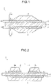
- Fig. 1 is a cross-sectional schematic diagram illustrating a configuration example of a circuit substrate.
- the circuit substrate 1 illustrated in Fig. 1 has a ceramic substrate 2, a metal plate (front metal plate) 3, a metal plate 4 (back metal plate), a bonding layer 5, and a bonding layer 7.
- the bonding layer 5 has a protruding portion 6.
- the bonding layer 7 has a protruding portion 8.
- a three-point bending strength of the ceramic substrate 2 is 500 MPa or more.
- a thickness of the ceramic substrate 2 can be reduced to 0.4 mm or less. If the ceramic substrate having a three-point bending strength of less than 500 MPa is thinned to 0.4 mm or less, a TCT characteristic is reduced. In particular, durability when a temperature on a high temperature side in a TCT is 175°C or more is reduced.
- the ceramic substrate having the three-point bending strength of 500 MPa or more it is preferable to use a silicon nitride substrate.
- Three-point bending strengths of an aluminum nitride substrate and an alumina substrate are about 300 to 450 MPa in general.
- the silicon nitride substrate has a high three-point bending strength of 500 MPa or more, and further, 600 MPa or more.
- the three-point bending strength is measured, for example, based on JIS-R-1601.
- the silicon nitride substrate has a heat conductivity of 50 W/m ⁇ K or more, and further, 80 W/m ⁇ K or more.
- the heat conductivity is measured, for example, based on JIS-R-1611.
- a recent silicon nitride substrate has both high strength and high heat conductivity.
- the silicon nitride substrate having the three-point bending strength of 500 MPa or more and the heat conductivity of 80 W/m ⁇ K or more enables reduction of a thickness of the ceramic substrate 2 to 0.30 mm or less.
- the ceramic substrate 2 it is possible to use not only the silicon nitride substrate but also an aluminum nitride substrate, an alumina substrate, an alumina substrate containing zirconia, and so on which have high strengths.
- the metal plate 3 is a metal circuit board for mounting a semiconductor element thereon.
- the metal plate 3 is bonded to a first surface of the ceramic substrate 2 via the bonding layer 5.
- the metal plate 4 is a heat sink plate.
- the metal plate 4 is bonded to a second surface of the ceramic substrate 2 via the bonding layer 7.
- metal plates 3, 4 metal plates containing copper or aluminum or an alloy whose main component is copper or aluminum can be used.
- the metal plate of the above-described material since being low in electrical resistance, is easily usable as a circuit substrate, for example. Further, a heat conductivity of copper is as high as 398 W/m ⁇ K and a heat conductivity of aluminum is as high as 237 W/m ⁇ K. Thus, heat release performance can also be improved.
- Thicknesses of the metal plates 3, 4 having the above-described characteristics are preferable to be 0.6 mm or more, and further, 0.8 mm or more. Increasing the thickness of the metal plate can achieve both securing of a current-carrying capacity and improvement of heat release performance. Further, heat can be diffused not only in a thickness direction of the metal plate but also in a surface direction, so that the heat release performance can be improved.
- the thickensses of the metal plates 3, 4 are preferable to be 5 mm or less. The thickness over 5 mm excessively increases a weight of the metal plate, resulting in apprehension that adjustment of sizes of the protruding portions 6, 8 becomes difficult.
- the bonding layer 5 bonds the first surface of the ceramic substrate 2 and the metal plate 3.
- the bonding layer 6 bonds the second surface of the ceramic substrate 2 and the metal plate 4.
- the protruding portion 6 extends onto the first surface of the ceramic substrate 2 in a manner to protrude from between the first surface and the metal plate 3.
- the protruding portion 8 extends onto the second surface of the ceramic substrate 2 in a manner to protrude from between the second surface and the metal plate 4.
- the bonding layers 5, 7 are formed by applying brazing material paste onto the ceramic substrate 2.
- the brazing material paste spreads too much due to weights of the metal plates 3, 4. Too much spreading of the brazing material paste increases a brazing material amount to be removed by an etching processing or the like after bonding, to cause a cost increase. Therefore, the thicknesses of the metal plates 3, 4 are preferable to be 5 mm or less, and further, 3 mm or less.
- the bonding layers 5, 7 are preferable to contain at least one element selected from Ag (silver), Cu (copper), and Al (aluminum) as a main component. Further, the bonding layers 5, 7 are preferable to further contain at least one element selected from Ti (titanium), Hf (hafnium), Zr (zirconium), Si (silicon), and Mg (magnesium). For example, the bonding layers 5, 7 may contain Ag, Cu, and at least one element selected from Ti, Zr, and Hf. Further, the bonding layers 5, 7 may contain Al and at least one element selected from Si and Mg.
- the bonding layer whose main component is Ag or Cu is suitable for bonding a copper plate. The copper plate has a higher heat conductivity compared with an aluminum plate, and is effective in improving heat release performance. Further, the bonding layers 5, 7 are preferable to contain at least one element selected from In (indium), Sn (tin), and C (carbon).
- At least one of a ratio L1/H1 of a protruding length L1 ( ⁇ m) to a thickness H1 ( ⁇ m) of the protruding portion 6 and a ratio L2/H2 of a protruding length L2 ( ⁇ m) to a thickness H2 ( ⁇ m) of the protruding portion 8 is 0.5 or more and 3.0 or less. At least one of L1/H1 and L2/H2 being 0.5 or more and 3.0 or less indicates that the protruding length (width) is 0.5 times or more and 3.0 times or less the thickness.
- a heat stress is applied to the protruding portions 6, 8.
- the heat stress becomes larger as a temperature difference between a low temperature side and a high temperature side of the TCT spreads.
- the protruding lengths of the protruding portions 6, 8 are small when L1/H1 and L2/H2 are less than 0.5, and thus the heat stress applied to the protruding portions 6, 8 becomes large in the thickness direction.
- the above causes generation of a crack inside the ceramic substrate 2 and the bonding layers 5, 7 due to the heat stress.
- L1/H1 and L2/H2 are over 3.0, the heat stress applied to the protruding portions 6, 8 becomes large in a protruding length direction. The above causes generation of a crack inside the ceramic substrate 2 and the bonding layers 5, 7 due to the heat stress.
- the heat stress is generated by shrinkage and expansion occurring due to the temperature difference.
- L1/H1 and L2/H2 homogeneity in a direction to which the heat stress (shrinkage and expansion) is applied can be increased, and thus, the crack occurring inside the ceramic substrate 2 and the bonding layers 5, 7 can be suppressed. Consequently, the TCT characteristic can be improved.
- L1/H1 and L2/H2 are more preferable to be 1.0 or more and 2.0 or less.
- At least one of average values of Vickers hardnesses of arbitrary 10 places of the protruding portion 6 and of Vickers hardnesses of arbitrary 10 places of the protruding portion 8 is 883 MPa (90 kgf/mm 2 ) or more and 2256 MPa (230 kgf/mm 2 ) or less.
- the average value of the Vickers hardnesses is over 2452 MPa (250 kgf/mm 2 )
- the protruding portions 6, 8 become too hard to obtain alleviation effects of heat stress sufficiently.
- the average value of the Vickers hardnesses is preferable 981 MPa (100 kgf/mm 2 ) or more and 1667 MPa (170 kgf/mm 2 ) or less.
- the hardness of the protruding portion is insufficient. There is apprehension that excessive softness may make a deformation amount due to the heat stress larger, contrarily. The large deformation amount may bring about deterioration of the TCT characteristic.
- At least one of a difference between a maximum value and a minimum value of Vickers hardnesses of the arbitrary 10 places of the protruding portion 6 and a difference between a maximum value and a minimum value of Vickers hardnesses of the arbitrary 10 places of the protruding portion 8 is 490 MPa (50 kgf/mm 2 ) or less. Large variation of Vickers hardnesses generates partial variation of deformation amounts due to the heat stress. Thus, the variation of Vickers hardnesses is preferable to be small.
- the Vickers hardness is measured based on JIS-R-1610. A load by an indenter is applied to the protruding portions 6, 8 at a load of 0.49 N (50 gf) for a load holding time of 10 seconds. The Vickers hardness is obtained from diagonal line lengths in 2 directions of an indentation.
- the Vickers hardness is measured by using a nano indenter. If the nano indenter is used, the Vickers hardness can be measured without removing the metal plate.
- a nano indenter manufactured by Hysitron, Inc. can be used, for example.
- a Berkovich type diamond triangular pyramid indenter can be used, for example. With a maximum load being set to 1500 ⁇ N (micro Newton), an indentation depth at a time that the load is gradually increased over 50 seconds is measured, and a nano indentation hardness HIT is obtained.
- the circuit substrate of the invention is a circuit substrate obtained by bonding the ceramic substrate having the three-point bending strength of 500 MPa or more and the metal plates on both surfaces thereon via the bonding layers.
- the bonding layer has the protruding portion, and the ratio of the protruding length to the thickness of the protruding portion is 0.5 or more and 3.0 or less, and the average value of the Vickers hardnesses of 10 places of the protruding portion is 883 MPa (90 kgf/mm 2 ) or more and 2256 MPa (230 kgf/mm 2 ) or less.
- FIG. 2 is a cross-sectional schematic diagram illustrating another configuration example of the circuit substrate.
- a circuit substrate 1 illustrated in Fig. 2 is different compared with the circuit substrate 1 illustrated in Fig. 1 at least in configuration where a metal plate 3a and a metal plate 3b are included as the plurality of metal plates 3.
- the circuit substrate 1 may have three or more metal plates as the plurality of metal plates 3. Note that regarding explanation of the same configuration as that of the circuit substrate 1 illustrated in Fig. 1 , explanation of the circuit substrate 1 illustrated in Fig. 1 is appropriately cited.
- the metal plate 3a is bonded to a first surface of a ceramic substrate 2 via a bonding layer 5a.
- the metal plate 3b is bonded to the first surface of the ceramic substrate 2 via a bonding layer 5b.
- explanation of the bonding layer 5a and the bonding layer 5b explanation of the bonding layer 5 is appropriately cited.
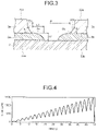
- Fig. 3 is an enlarged diagram illustrating a part of the circuit substrate 1 illustrated in Fig. 2 .
- the bonding layer 5a has a protruding portion 6a extending onto the first surface of the ceramic substrate 2 in a manner to protrude from between the first surface and the metal plate 3a.
- the bonding layer 5b has a protruding portion 6b extending onto the first surface of the ceramic substrate 2 in a manner to protrude from between the first surface and the metal plate 3b.
- a side surface 31a of the metal plate 3 is inclined toward the edge of an outer surface 32a of the metal plate 3.
- a side surface 31b of the metal plate 3 is inclined toward the edge of an outer surface 32b of the metal plate 3.
- An angle ⁇ made by the side surface 31a and a inner surface 33a of the metal plate 3a and an angle ⁇ made by the side surface 31b and a inner surface 33b of the metal plate 3b are preferable to be 40 degrees or more and 84 degrees or less.
- An angle made by the side surface 31a and the outer surface 32a of the metal plate 3a and an angle made by the side surface 31b and the outer surface 32b of the metal plate 3b are preferable to be 85 degrees or more and 95 degrees or less (perpendicular or almost perpendicular).
- a structure illustrated in Fig. 3 is effective in particular when thicknesses of the metal plates 3a, 3b are 0.6 mm or more, and further, 0.8 mm or more.
- the protruding length of the protruding portion is obtained with a contact portion of the side surface of the metal plate and the protruding portion being a reference.
- the thickness of the protruding portion is a thickness of the thickest part of the protruding portion.
- a thickness of the protruding portion 6a at a contact portion of the side surface 31a and the protruding portion 6a and a thickness of the protruding portion 6b at a contact portion of the side surface 31b and the protruding portion 6b are thickest, that the protruding portion 6a has a thickness gradient of becoming gradually thinner from the contact portion of the side surface 31a and the protruding portion 6a toward an end portion, and that the protruding portion 6b has a thickness gradient of becoming gradually thinner from the contact portion of the side surface 31b and the protruding portion 6b toward an end portion.
- a protruding length L1 of the protruding portions 6a, 6b is preferable to be 40 ⁇ m or less, and further, 25 ⁇ m or less.
- L1/H1 of the protruding portions 6a, 6b and a Vickers hardness HV By controlling L1/H1 of the protruding portions 6a, 6b and a Vickers hardness HV, a stress alleviation effect can be improved. In other words, even with a protruding portion having a protruding length as short as 40 ⁇ m or less, a sufficient stress alleviation effect can be obtained.
- the circuit substrate illustrated in Fig. 3 is effective in a case where a plurality of metal plates are bonded to a first surface of a ceramic substrate 2.
- a minimum value of the shortest distance P is preferable to be 0.6 mm or more. In a case of a power module having a metal plate of 0.6 mm or more in thickness, conductivity failure may occur if the shortest distance P is less than 0.6 mm, considering a rated voltage.
- the above-described circuit substrate has a high TCT characteristic.
- a TCT is carried out, with one cycle being -40°C ⁇ holding for 30 minutes ⁇ room temperature ⁇ holding for 10 minutes ⁇ 175°C ⁇ holding for 30 minutes ⁇ room temperature ⁇ holding for 10 minutes, for example, by measuring the number of the cycles where a failure occurs in the circuit substrate.
- the failure of the circuit substrate means, for example, peeling of the bonding layers 5 (5a, 5b), 7, a crack of the ceramic substrate 2, or the like.
- the circuit substrate of this embodiment can exhibit an excellent TCT characteristic even if a holding temperature on a high temperature side in the TCT is set to 175°C or higher.
- the holding temperature of 175°C or higher means, for example, 200°C to 250°C.
- a junction temperature is estimated to become 200 to 250°C.
- the junction temperature corresponds to an operation guaranteed temperature of the semiconductor element. Thus, durability at a high temperature is required also of the circuit substrate.
- a ratio of the protruding length to the thickness of the protruding portion, and the Vickers hardness are controlled.
- the TCT characteristic can be improved even in a case of the circuit substrate in which a plurality of metal plates are bonded.
- the circuit substrate of this embodiment is effective as a circuit substrate for mounting a semiconductor element of a semiconductor device. Further, the circuit substrate of this embodiment is suitable also for a semiconductor device on which a plurality of semiconductor elements are mounted.
- the circuit substrate according to this embodiment since the shortest distance P between the metal plates can be made narrow, it is possible to reduce a size of a semiconductor device on which the same number of semiconductor elements are mounted. Therefore, the semiconductor device can be made smaller. Making the semiconductor device smaller leads to improvement of a power density.
- the manufacturing method of the circuit substrate according to the embodiment is not limited in particular, but the following method is cited as a method for obtaining the circuit substrate efficiently.
- a ceramic substrate 2 is prepared.
- a TiN phase titanium nitride phase
- the TiN phase contributes to improvement of a bonding strength.
- metal plates 3, 4 are prepared. Regarding the metal plates 3, 4, plain plates may be bonded and patterned by etching, or metal plates having been patterned in advance may be bonded.
- the brazing material is prepared for forming bonding layers 5, 7.
- a brazing material containing Ag, Cu and Ti is used for at least one of the bonding layers 5, 7.
- In and Sn it is preferable that at least one element selected from In and Sn are added in a range of 5 to 20 mass%.
- C it is preferable that C is added in a range of 0.1 to 3 mass%.
- compositions of the brazing material using Ti were explained here, part or all of Ti may be replaced by Zr or Hf.
- bonding layers 5, 7 which contain Ag, Cu, and at least one element selected from Ti, Zr, and Hf
- a brazing material containing respective elements Among active metals selected from Ti, Zr, and Hf, Ti is preferable.
- Ti can form TiN to form solid bonding. It is also effective to add at least one element selected from In (indium), Sn (tin), and C (carbon) to those brazing materials.
- an Ag-Cu-Ti brazing material is used, it is possible to bond the metal plates 3, 4 to the ceramic substrate 2 by using an eutectic of Ag-Cu.
- the Ag-Cu eutectic contains 72 mass% Ag and 28 mass% Cu. Thus, a mass ratio Ag/Cu is 2.57.
- a mass ratio Ag/Cu of a normal Ag-Cu-Ti brazing material is approximately 2.57.
- the Ag-Cu eutectic is a hard crystal. Increase of the Ag-Cu eutectic makes a bonding layer hard. Thus, hardnesses of the protruding portions 6, 8 also become high. Further, if the Ag-Cu eutectics are not formed uniformly, variation of the Vickers hardnesses also becomes large.
- a Cu amount can be made larger than a eutectic composition.
- the hardnesses of the protruding portions 6, 8 can be reduced.
- it is also effective to make a brazing material contain at least one element selected from In, Sn, and C.
- the brazing material using In or Sn bonding at a low temperature is possible (a melting point of the brazing material is lowered), and a residual stress of a bonded body can be decreased. Decrease of the residual stress is effective in improvement of heat cycle reliability of the bonded body.
- a content of at least one element selected from In and Sn is less than 5 mass%, sufficient effect of addition is difficult to be obtained. Meanwhile, the content over 20 mass% leads to apprehension that the bonding layer becomes too hard.
- C is effective in reducing variation of hardnesses of a bonding layer.
- C can control fluidity of a brazing material. By adding 0.1 to 2 mass% C to the brazing material, fluidity can be suppressed. Therefore, variation of hardnesses of the bonding layer can be made smaller. When an added amount of C is less than 0.1 mass%, an effect of addition is insufficient. Meanwhile, when the added amount of C is over 2 mass%, the bonding layer may become too hard.
- Ti is preferable to be added in a range of 1 to 12 mass%, and further, 5 to 11 mass%.
- Ti reacts to nitrogen of a silicon nitride substrate, for example, to form a TiN (titanium nitride) phase.
- a bonding strength can be improved. Bonding strengths (peel strengths) of the metal plates 3, 4 can be made as high as 17 kN/m or more, and further, 20 kN/m or more.
- a Ti amount is preferable to be set to 5 mass% or more.
- Increasing the Cu amount leads to reduction of the amount of the Ag-Cu eutectic, by which an alleviation effect of a heat stress can be suppressed from becoming insufficient as a result that the protruding portion becomes too hard.
- increasing the Ti amount makes it easy to form an Ag-Ti crystal and Cu-Ti crystal at a time of heating the brazing material. Melting points of the Ag-Ti crystal and of the Cu-Ti crystal are close to each other. Therefore, setting the mass ratio Ag/Cu to 2.4 or less can prevent melting points of brazing material structures from varying due to increase of Cu. By this effect, it is possible to reduce variation of Vickers hardnesses. Further, though a case where Ti is used is explained here, the same applies to a case where Zr or Hf is used.
- brazing material paste in which the above-described components of the brazing material are mixed homogeneously.
- a metal component in the brazing material paste is set to 60 to 95 mass% or less. The remaining 5 to 40 mass% is accounted for by a resin binder, an organic solvent, or the like. By setting the metal component to 90 mass% or more, unevenness of coating can be made small.
- the brazing material paste is applied to first and second surfaces of the ceramic substrate 2, the metal plate 3 is disposed on a brazing material paste layer on the first surface, and the metal plate 4 is disposed on a brazing material paste layer on the second surface.
- a method may be one where the brazing material paste is applied onto the metal plates 3, 4 and the ceramic substrate 2 is disposed thereon. Regions to become the protruding portions 6, 8 may be small. Further, the protruding portions 6, 8 may be formed by an etching process as will be described later.
- circuit substrate of five layer structure of metal plate 3/blazing material paste layer (bonding layer 5)/ceramic substrate 2/blazing material paste layer (bonding layer 7)/metal plate 4.
- a heating temperature is in a range of 700 to 900°C, for example. Further, it is preferable to cool rapidly at a cooling rate of 5°C/min or more after heat bonding. A rapid cooling process is preferable to be carried out to a temperature of equal to or lower than a freezing point temperature of the bonding layers 5, 7. By carrying out the rapid cooling process, the bonding layers 5, 7 can be solidified early. As a result that the brazing material melted by the heating process is solidified early and becomes the bonding layers 5, 7, variation of Vickers hardnesses can be reduced.
- an etching process is carried out as necessary. Patterning of the metal plates 3, 4 is carried out by the etching process. Side surfaces of the metal plates 3, 4 may be inclined by the etching process. Further, protruding lengths and thicknesses of the protruding portions 6, 8 may be adjusted by the etching process. The process to etch the metal plates 3, 4 and the etching process to arrange shapes of the protruding portions 6, 8 may be the same process or different processes.
- the circuit substrate can be manufactured efficiently. Further, it is possible to mount the necessary number of semiconductor elements on the circuit substrate to manufacture a semiconductor device.
- Ceramic substrates 1 to 4 having characteristics shown in Table 1 are prepared as ceramic substrates, and brazing materials shown in Table 2 are prepared as brazing materials.
- a quality of material in Table 1 means a material of a major component of the ceramic substrate.
- silicon nitride indicates a ceramic substrate whose main component is silicon nitride.
- Allumina zirconia indicates a ceramic substrate whose main component is aluminum oxide containing ZrO 2 (zirconium oxide).
- Al indicates a ceramic substrate whose main component is aluminum oxide.
- a front metal plate was disposed on a first surface of the ceramic substrate via a first brazing material
- a back metal plate was disposed on a second surface of the ceramic substrate via a second brazing material
- heat bonding was carried out at 700 to 900°C
- cooling was carried out at a cooling rate of 5°C/min or more after heat bonding.
- etching was carried out to adjust a protruding length L ( ⁇ m) and a thickness H ( ⁇ m) of a protruding portion, and a shortest distance P between the metal plates.
- Table 3 shows the ceramic substrates, first brazing materials, and second brazing materials which were used in the circuit substrates of Examples 1 to 13.
- Tables 3, 4 show other characteristics of the circuit substrates of Examples 1 to 13 and Comparative Examples 1 to 4. Note that copper plates were used as the metal plates of Examples 1 to 3, Examples 5 to 13, and Comparative Examples 1 to 4. An aluminum plate was used as the metal plate of Example 4.
- Ceramic Substrate First And Second Brazing Materials Metal Plate Front Metal Plate P (mm) Back Metal Plate (Vertical Length (mm) ⁇ Horizontal Length (mm) ⁇ Thickness (mm)) (Vertical Length (mm) ⁇ Horizontal Length (mm) ⁇ Thickness (mm)) Number
- Example 1 ⁇ Ceramic Substrate 1 Brazing Material 2 20 ⁇ 35 ⁇ 0.8 2 1.1 45 ⁇ 35 ⁇ 0.6
- Example 4 Ceramic Substrate 1 Brazing Material 5 20 ⁇ 35 ⁇ 0.8 2 1.1 45 ⁇ 35 ⁇ 0.6
- Example 5 Ceramic Substrate 2 Brazing Material 2 20 ⁇ 35 ⁇ 0.8 2 1.1 45 ⁇ 35 ⁇ 0.6
- Example 6 Ceramic Substrate 2 Brazing Material 3 20 ⁇ 35 ⁇ 0.8 2 1.0 45 ⁇ 35 ⁇ 0.8
- Example 7 Ceramic Substrate 2 Brazing
- a Vickers hardness HV of an arbitrary protruding portion of the obtained circuit substrate was measured.
- TI 950 TriboIndenter manufactured by Hysitron, Inc. was used as a nano indenter, and a Berkovich type diamond triangular pyramid indenter was used as an indenter.
- Fig. 4 illustrates a load condition.
- a horizontal axis indicates a time (second) and a vertical axis indicates a load ( ⁇ N).
- a maximum load is 1500 ⁇ N and the load was increased gradually over 50 seconds.
- An indentation depth at this time was measured to obtain a nano indentation hardness HIT.
- the nano indentation hardness HIT was converted into a Vickers hardness HV by using the following conversion formula.
- Vickers hardness HV kgf / mm 2 76.23 ⁇ nano indentation hardness HIT GPa + 6.3
- Vickers hardnesses HV of arbitrary 10 places were calculated and an average value thereof was obtained. Further, a difference (HV max - HV min ) between a maximum value and a minimum value of the Vickers hardnesses of 10 places was obtained. Results are shown in Table 4.
- bonding strengths of arbitrary metal plates and TCT characteristics were measured.
- the bonding strength of the metal plate was obtained as a peel strength. More specifically, a metal terminal of 1 mm in width is bonded to the metal plate and pulled in a perpendicular direction, to measure the peel strength.
- TCTs were carried out under two kinds of conditions.
- a test 1 with one cycle being -40°C ⁇ holding for 30 minutes ⁇ room temperature ⁇ holding for 10 minutes ⁇ 125°C ⁇ holding for 30 minutes ⁇ room temperature ⁇ holding for 10 minutes, existence/absence of a defect of the circuit substrate after 3000 cycles was measured.
- a test 2 with one cycle being -40°C ⁇ holding for 30 minutes ⁇ room temperature ⁇ holding for 10 minutes ⁇ 250°C ⁇ holding for 30 minutes ⁇ room temperature ⁇ holding for 10 minutes, existence/absence of a defect of the circuit substrate after 3000 cycles was measured.
Landscapes
- Engineering & Computer Science (AREA)
- Microelectronics & Electronic Packaging (AREA)
- Chemical & Material Sciences (AREA)
- Inorganic Chemistry (AREA)
- Ceramic Engineering (AREA)
- Manufacturing & Machinery (AREA)
- Materials Engineering (AREA)
- Structural Engineering (AREA)
- Organic Chemistry (AREA)
- Ceramic Products (AREA)
- Cooling Or The Like Of Semiconductors Or Solid State Devices (AREA)
- Structure Of Printed Boards (AREA)
Claims (20)
- Schaltkreissubstrat (1), umfassend:ein Keramiksubstrat (2), welches eine erste Oberfläche und eine zweite Oberfläche umfasst;eine erste Metallplatte (3), welche über eine erste Bindeschicht (5) mit der ersten Oberfläche verbunden ist; undeine zweite Metallplatte (4), welche über eine zweite Bindeschicht (7) mit der zweiten Oberfläche verbunden ist,wobei die erste Bindeschicht (5) einen ersten Abschnitt (6) aufweist, welcher zwischen der ersten Oberfläche und der ersten Metallplatte (3) hervorsteht und sich auf die erste Oberfläche erstreckt,wobei die zweite Bindeschicht (7) einen zweiten Abschnitt (8) aufweist, welcher zwischen der zweiten Oberfläche und der zweiten Metallplatte (4) hervorsteht und sich auf die zweite Oberfläche erstreckt,wobei zumindest eine ausgewählt aus der ersten Bindeschicht (5) und der zweiten Bindeschicht (7) Ag, Cu und Ti enthält,wobei die Dreipunkt-Biegefestigkeit des Keramiksubstrats (2) 500 MPa oder mehr beträgt, undwobei zumindest eines ausgewählt aus dem Verhältnis L1/H1 einer Länge L1 (µm) des ersten Abschnitts (6) zu einer Dicke H1 (µm) hiervon und dem Verhältnis L2/H2 einer Länge L2 (µm) des zweiten Abschnitts (8) zu einer Dicke H2 (µm) hiervon 0.5 oder mehr und 3.0 oder weniger beträgt,dadurch gekennzeichnet, dass zumindest einer ausgewählt aus dem Mittelwert erster Vickers-Härten von 10 Stellen des ersten Abschnitts (6) und dem Mittelwert zweiter Vickers-Härten von 10 Stellen des zweiten Abschnitts (8) 883 MPa (90 kgf/mm2) oder mehr und 2256 MPa (230 kgf/mm2) oder weniger beträgt.
- Schaltkreissubstrat (1) gemäß Anspruch 1, wobei zumindest einer ausgewählt aus dem Mittelwert der ersten Vickers-Härten und dem Mittelwert der zweiten Vickers-Härten 981 MPa (100 kgf/mm2) oder mehr und 1667 MPa (170 kgf/mm2) oder weniger beträgt.
- Schaltkreissubstrat (1) gemäß Anspruch 1, wobei zumindest eines ausgewählt aus dem Verhältnis L1/H1 und dem Verhältnis L2/H2 1.0 oder mehr und 2.0 oder weniger beträgt.
- Schaltkreissubstrat (1) gemäß Anspruch 1, wobei es sich bei dem Keramiksubstrat (2) um ein Siliziumnitridsubstrat handelt.
- Schaltkreissubstrat (1) gemäß Anspruch 1,wobei es sich bei zumindest einer ausgewählt aus der ersten Metallplatte (3) und der zweiten Metallplatte (4) um eine Kupferplatte handelt,wobei die Dicke der Kupferplatte 0.6 mm oder mehr beträgt, undwobei die Dicke des Keramiksubstrats (2) 0.4 mm oder weniger beträgt.
- Schaltkreissubstrat (1) gemäß Anspruch 1, wobei zumindest eine ausgewählt aus der Länge L1 und der Länge L2 40 µm oder weniger beträgt.
- Schaltkreissubstrat (1) gemäß Anspruch 1,wobei eine Seitenoberfläche (31) der ersten Metallplatte (3), in einem Querschnitt der ersten Metallplatte (3) entlang einer Dickenrichtung hiervon, in Richtung des Rands einer Außenoberfläche (32) der ersten Metallplatte (3) geneigt ist, undwobei eine Seitenoberfläche der zweiten Metallplatte (4), in einem eine Dickenrichtung der zweiten Metallplatte (4) umfassenden Querschnitt, in Richtung des Rands einer Außenoberfläche der zweiten Metallplatte (4) geneigt ist.
- Schaltkreissubstrat (1) gemäß Anspruch 1, wobei zumindest eine ausgewählt aus der Differenz zwischen einem Maximalwert und einem Minimalwert der ersten Vickers-Härten und der Differenz zwischen einem Maximalwert und einem Minimalwert der zweiten Vickers-Härten 490 MPa (50 kgf/mm2) oder weniger beträgt.
- Schaltkreissubstrat (1) gemäß Anspruch 1, wobei sowohl die erste Bindeschicht (5) als auch die zweite Bindeschicht (7) Ag, Cu und Ti enthält.
- Schaltkreissubstrat (1) gemäß Anspruch 9, wobei zumindest eine ausgewählt aus der ersten Bindeschicht (5) und der zweiten Bindeschicht (7) weiterhin zumindest ein Element ausgewählt aus der Gruppe bestehend aus In, Sn und C enthält.
- Schaltkreissubstrat (1) gemäß Anspruch 1, umfassend eine Vielzahl der ersten Metallplatten (3).
- Schaltkreissubstrat (1) gemäß Anspruch 1, umfassend eine Vielzahl der ersten Metallplatten (3), wobei der kürzeste Abstand zwischen einer der ersten Metallplatten (3a) und einer anderen der ersten Metallplatten (3b) 1.1 mm oder weniger beträgt.
- Schaltkreissubstrat (1) gemäß Anspruch 1, wobei es sich bei dem Keramiksubstrat (2) um ein Siliziumnitridsubstrat mit einer Wärmeleitfähigkeit von 80 W/m·K oder mehr und einer Dicke von 0.30 mm oder weniger handelt.
- Schaltkreissubstrat (1) gemäß Anspruch 1,wobei es sich bei dem Keramiksubstrat (2) um ein Siliziumnitridsubstrat mit einer Wärmeleitfähigkeit von 80 W/m·K oder mehr und einer Dicke von 0.30 mm oder weniger handelt, undwobei es sich bei zumindest einer ausgewählt aus der ersten Metallplatte (3) und der zweiten Metallplatte (4) um eine Kupferplatte mit einer Dicke von 0.6 mm oder mehr handelt.
- Schaltkreissubstrat (1) gemäß Anspruch 1, umfassend eine Vielzahl der ersten Metallplatten (3),wobei es sich bei dem Keramiksubstrat (2) um ein Siliziumnitridsubstrat mit einer Wärmeleitfähigkeit von 80 W/m·K oder mehr und einer Dicke von 0.30 mm oder weniger handelt,wobei es sich bei zumindest einer ausgewählt aus der ersten Metallplatte (3) und der zweiten Metallplatte (4) um eine Kupferplatte mit einer Dicke von 0.6 mm oder mehr handelt, undwobei der kürzeste Abstand zwischen einer der ersten Metallplatten (3a) und einer anderen der ersten Metallplatten (3b) 1.1 mm oder weniger beträgt.
- Schaltkreissubstrat (1) gemäß Anspruch 1, wobei das Massenverhältnis von Silber zu Kupfer in zumindest einem ausgewählt aus dem ersten Abschnitt (6) und dem zweiten Abschnitt (8) 2.4 oder weniger beträgt.
- Schaltkreissubstrat (1) gemäß Anspruch 1,wobei es sich bei zumindest einer ausgewählt aus der ersten Metallplatte (3) und der zweiten Metallplatte (4) um eine Kupferplatte mit einer Dicke von 0.6 mm oder mehr handelt, undwobei das Massenverhältnis von Silber zu Kupfer in zumindest einem ausgewählt aus dem ersten Abschnitt (6) und dem zweiten Abschnitt (8) 2.4 oder weniger beträgt.
- Schaltkreissubstrat (1) gemäß Anspruch 1, umfassend eine Vielzahl der ersten Metallplatten (3),wobei das Massenverhältnis von Silber zu Kupfer in zumindest einem ausgewählt aus dem ersten Abschnitt (6) und dem zweiten Abschnitt (8) 2.4 oder weniger beträgt,wobei es sich bei dem Keramiksubstrat (2) um ein Siliziumnitridsubstrat mit einer Wärmeleitfähigkeit von 80 W/m·K oder mehr und einer Dicke von 0.30 mm oder weniger handelt,wobei es sich bei zumindest einer ausgewählt aus der ersten Metallplatte (3) und der zweiten Metallplatte (4) um eine Kupferplatte mit einer Dicke von 0.6 mm oder mehr handelt, undwobei der kürzeste Abstand zwischen einer der ersten Metallplatten (3a) und einer anderen der ersten Metallplatten (3b) 1.1 mm oder weniger beträgt.
- Halbleitervorrichtung, umfassend:das Schaltkreissubstrat (1) gemäß Anspruch 1; undein Halbleiterelement, welches auf dem Schaltkreissubstrat (1) befestigt ist.
- Halbleitervorrichtung gemäß Anspruch 19, umfassend eine Vielzahl der Halbleiterelemente.
Priority Applications (1)
| Application Number | Priority Date | Filing Date | Title |
|---|---|---|---|
| EP19210462.8A EP3629370B1 (de) | 2015-09-28 | 2016-08-01 | Schaltkreissubstrat und halbleiterbauelement |
Applications Claiming Priority (2)
| Application Number | Priority Date | Filing Date | Title |
|---|---|---|---|
| JP2015189990 | 2015-09-28 | ||
| PCT/JP2016/003531 WO2017056360A1 (ja) | 2015-09-28 | 2016-08-01 | 回路基板および半導体装置 |
Related Child Applications (2)
| Application Number | Title | Priority Date | Filing Date |
|---|---|---|---|
| EP19210462.8A Division EP3629370B1 (de) | 2015-09-28 | 2016-08-01 | Schaltkreissubstrat und halbleiterbauelement |
| EP19210462.8A Division-Into EP3629370B1 (de) | 2015-09-28 | 2016-08-01 | Schaltkreissubstrat und halbleiterbauelement |
Publications (3)
| Publication Number | Publication Date |
|---|---|
| EP3358614A1 EP3358614A1 (de) | 2018-08-08 |
| EP3358614A4 EP3358614A4 (de) | 2019-05-22 |
| EP3358614B1 true EP3358614B1 (de) | 2022-12-14 |
Family
ID=58423198
Family Applications (2)
| Application Number | Title | Priority Date | Filing Date |
|---|---|---|---|
| EP16850544.4A Active EP3358614B1 (de) | 2015-09-28 | 2016-08-01 | Schaltsubstrat und halbleiterbauelement |
| EP19210462.8A Active EP3629370B1 (de) | 2015-09-28 | 2016-08-01 | Schaltkreissubstrat und halbleiterbauelement |
Family Applications After (1)
| Application Number | Title | Priority Date | Filing Date |
|---|---|---|---|
| EP19210462.8A Active EP3629370B1 (de) | 2015-09-28 | 2016-08-01 | Schaltkreissubstrat und halbleiterbauelement |
Country Status (6)
| Country | Link |
|---|---|
| US (2) | US10515868B2 (de) |
| EP (2) | EP3358614B1 (de) |
| JP (2) | JP6789955B2 (de) |
| KR (1) | KR101949069B1 (de) |
| CN (2) | CN110690187B (de) |
| WO (1) | WO2017056360A1 (de) |
Families Citing this family (45)
| Publication number | Priority date | Publication date | Assignee | Title |
|---|---|---|---|---|
| JP6789955B2 (ja) * | 2015-09-28 | 2020-11-25 | 株式会社東芝 | 回路基板および半導体装置 |
| WO2017213207A1 (ja) * | 2016-06-10 | 2017-12-14 | 田中貴金属工業株式会社 | セラミックス回路基板、及び、セラミックス回路基板の製造方法 |
| JP7013374B2 (ja) * | 2016-07-28 | 2022-01-31 | 株式会社東芝 | 接合体、回路基板、および半導体装置 |
| JP7052374B2 (ja) | 2017-02-06 | 2022-04-12 | 三菱マテリアル株式会社 | セラミックス/アルミニウム接合体の製造方法、絶縁回路基板の製造方法 |
| US20190006254A1 (en) * | 2017-06-30 | 2019-01-03 | Kyocera International, Inc. | Microelectronic package construction enabled through ceramic insulator strengthening and design |
| US11483926B2 (en) | 2017-07-25 | 2022-10-25 | Denka Company Limited | Ceramic circuit board and production method therefor |
| EP3684148B1 (de) | 2017-09-12 | 2023-11-29 | Kabushiki Kaisha Toshiba | Verfahren zur herstellung einer keramischen leiterplatte |
| CN111032916A (zh) | 2017-09-12 | 2020-04-17 | 株式会社东芝 | 活性金属钎料用蚀刻液及使用了其的陶瓷电路基板的制造方法 |
| CN112166654B (zh) * | 2018-05-16 | 2024-07-26 | 株式会社东芝 | 陶瓷铜电路基板及其制造方法 |
| JP6446155B1 (ja) * | 2018-07-17 | 2018-12-26 | 株式会社日立パワーソリューションズ | 両面回路非酸化物系セラミックス基板およびその製造方法 |
| DE102018212272A1 (de) * | 2018-07-24 | 2020-01-30 | Robert Bosch Gmbh | Keramischer Schaltungsträger und Elektronikeinheit |
| CN112313191B (zh) * | 2018-08-03 | 2022-11-15 | 株式会社东芝 | 氮化硅烧结体、氮化硅基板及氮化硅电路基板 |
| EP3846596B1 (de) | 2018-08-29 | 2025-07-30 | Kabushiki Kaisha Toshiba | Siliciumnitridsubstrat und siliciumnitridleiterplatte |
| EP3860317B1 (de) * | 2018-09-27 | 2024-07-24 | Denka Company Limited | Gebondetes substrat, metallleiterplatte und leiterplatte |
| EP3941166A4 (de) * | 2019-03-14 | 2022-11-09 | NGK Insulators, Ltd. | Gebundenes substrat |
| WO2020196746A1 (ja) * | 2019-03-26 | 2020-10-01 | 三菱マテリアル株式会社 | 絶縁回路基板 |
| WO2020208698A1 (ja) | 2019-04-09 | 2020-10-15 | 日本碍子株式会社 | 接合基板及び接合基板の製造方法 |
| JP7790968B2 (ja) * | 2019-04-11 | 2025-12-23 | 株式会社Niterra Materials | セラミックス銅回路基板およびそれを用いた半導体装置 |
| KR20220066051A (ko) * | 2019-09-20 | 2022-05-23 | 덴카 주식회사 | 회로 기판 및 이것을 구비하는 모듈 |
| EP4108377A4 (de) * | 2020-02-17 | 2024-02-07 | Kabushiki Kaisha Toshiba | Hartlötfüllmaterial, verbundener körper, keramische leiterplatte und verfahren zur herstellung eines verbundenen körpers |
| JP7470181B2 (ja) * | 2020-03-18 | 2024-04-17 | 株式会社東芝 | 接合体、セラミックス銅回路基板、接合体の製造方法、およびセラミックス銅回路基板の製造方法 |
| JP7103529B2 (ja) * | 2020-06-03 | 2022-07-20 | 住友ベークライト株式会社 | 回路基板 |
| JP7672204B2 (ja) * | 2020-07-15 | 2025-05-07 | Dowaメタルテック株式会社 | 絶縁基板およびその製造方法 |
| JP7446430B2 (ja) * | 2020-07-22 | 2024-03-08 | 京セラ株式会社 | 回路基板 |
| JP7644763B2 (ja) | 2020-07-27 | 2025-03-12 | 株式会社東芝 | 接合体、回路基板、半導体装置、及び接合体の製造方法 |
| CN116134607B (zh) | 2020-07-27 | 2025-03-11 | 株式会社东芝 | 接合体、电路基板、半导体装置及接合体的制造方法 |
| EP4234517B1 (de) | 2020-10-20 | 2025-10-01 | Kabushiki Kaisha Toshiba | Verbundener körper, keramische leiterplatte damit und halbleiterbauelement |
| EP4270467A4 (de) | 2020-12-24 | 2025-03-12 | Kabushiki Kaisha Toshiba | Isolierte leiterplatte und halbleiterbauelement damit |
| JP7642678B2 (ja) | 2020-12-24 | 2025-03-10 | 株式会社東芝 | 絶縁性回路基板およびそれを用いた半導体装置 |
| WO2022176777A1 (ja) | 2021-02-17 | 2022-08-25 | 株式会社 東芝 | セラミックス回路基板およびそれを用いた半導体装置 |
| WO2022210507A1 (ja) | 2021-03-30 | 2022-10-06 | 株式会社 東芝 | セラミックス回路基板の製造方法 |
| JP7793893B2 (ja) * | 2021-04-19 | 2026-01-06 | 三菱マテリアル株式会社 | 銅/セラミックス接合体、および、絶縁回路基板 |
| JPWO2022244769A1 (de) | 2021-05-19 | 2022-11-24 | ||
| JP7739105B2 (ja) * | 2021-09-21 | 2025-09-16 | Dowaメタルテック株式会社 | 金属-セラミックス接合基板およびその製造方法 |
| WO2023204167A1 (ja) | 2022-04-20 | 2023-10-26 | 株式会社 東芝 | セラミックス回路基板、半導体装置、及び半導体装置の使用方法 |
| JP7654164B2 (ja) | 2022-06-02 | 2025-03-31 | 株式会社東芝 | セラミックス回路基板およびそれを用いた半導体装置 |
| JP7815442B2 (ja) | 2022-07-05 | 2026-02-17 | 株式会社Niterra Materials | 接合体、セラミックス回路基板、半導体装置、及び接合体の製造方法 |
| CN120153477A (zh) * | 2022-10-21 | 2025-06-13 | 罗姆股份有限公司 | 半导体装置的冷却结构体 |
| JPWO2024150370A1 (de) * | 2023-01-12 | 2024-07-18 | ||
| EP4653111A1 (de) * | 2023-01-17 | 2025-11-26 | Kabushiki Kaisha Toshiba | Verfahren zur herstellung einer aktiven metallpaste, verfahren zur herstellung einer keramischen leiterplatte, verfahren zur herstellung einer halbleitervorrichtung |
| EP4654258A1 (de) | 2023-01-20 | 2025-11-26 | Kabushiki Kaisha Toshiba | Siliciumnitridsubstrat und siliciumnitridleiterplatte damit |
| WO2024171766A1 (ja) | 2023-02-17 | 2024-08-22 | 株式会社 東芝 | 接合体およびそれを用いたセラミックス回路基板 |
| WO2025013789A1 (ja) * | 2023-07-07 | 2025-01-16 | 株式会社 東芝 | セラミックス回路基板およびその製造方法 |
| WO2025216198A1 (ja) * | 2024-04-08 | 2025-10-16 | 株式会社Niterra Materials | セラミックス銅接合体、セラミックス銅回路基板、およびセラミックス銅接合体の製造方法 |
| WO2025263517A1 (ja) * | 2024-06-19 | 2025-12-26 | 株式会社Niterra Materials | 接合体、セラミックス回路基板、および半導体装置 |
Family Cites Families (21)
| Publication number | Priority date | Publication date | Assignee | Title |
|---|---|---|---|---|
| JPH09275165A (ja) * | 1996-02-07 | 1997-10-21 | Hitachi Ltd | 回路基板及びそれを用いた半導体装置 |
| US6936337B2 (en) * | 2001-09-28 | 2005-08-30 | Dowa Mining Co., Ltd. | Metal/ceramic circuit board |
| JP3648189B2 (ja) * | 2001-09-28 | 2005-05-18 | 同和鉱業株式会社 | 金属−セラミックス回路基板 |
| JP2004207587A (ja) * | 2002-12-26 | 2004-07-22 | Dowa Mining Co Ltd | 金属−セラミックス接合基板およびその製造方法 |
| JP3714557B2 (ja) * | 2003-04-21 | 2005-11-09 | 日立金属株式会社 | セラミックス基板用ろう材及びこれを用いたセラミックス回路基板、パワー半導体モジュール |
| JP4664816B2 (ja) * | 2003-09-25 | 2011-04-06 | 株式会社東芝 | セラミック回路基板、その製造方法およびパワーモジュール |
| JP4544964B2 (ja) * | 2004-10-27 | 2010-09-15 | 京セラ株式会社 | 放熱基板 |
| WO2007026547A1 (ja) | 2005-08-29 | 2007-03-08 | Hitachi Metals, Ltd. | 回路基板及びこれを用いた半導体モジュール、回路基板の製造方法 |
| JP4953797B2 (ja) | 2006-02-03 | 2012-06-13 | 株式会社エンプラス | 樹脂製品の成形方法 |
| JP5014642B2 (ja) | 2006-02-16 | 2012-08-29 | 株式会社トクヤマ | リード内蔵メタライズドセラミックス基板およびパッケージ |
| JPWO2007105361A1 (ja) * | 2006-03-08 | 2009-07-30 | 株式会社東芝 | 電子部品モジュール |
| JP4744385B2 (ja) * | 2006-07-28 | 2011-08-10 | 京セラ株式会社 | 放熱基板およびこれを用いた電子装置 |
| JP2009170930A (ja) * | 2009-03-12 | 2009-07-30 | Hitachi Metals Ltd | セラミックス回路基板及びこれを用いたパワー半導体モジュール |
| US9012783B2 (en) * | 2009-05-27 | 2015-04-21 | Kyocera Corporation | Heat dissipation base and electronic device |
| JP5675610B2 (ja) * | 2009-07-24 | 2015-02-25 | 株式会社東芝 | 窒化珪素製絶縁シートおよびそれを用いた半導体モジュール構造体 |
| HUE034429T2 (en) | 2009-09-15 | 2018-02-28 | Toshiba Kk | Ceramic circuit board and method for producing it |
| JP5133960B2 (ja) * | 2009-10-22 | 2013-01-30 | 電気化学工業株式会社 | 半導体搭載用回路基板及びその製造方法 |
| WO2013094213A1 (ja) * | 2011-12-20 | 2013-06-27 | 株式会社 東芝 | セラミックス銅回路基板とそれを用いた半導体装置 |
| KR102196949B1 (ko) | 2013-03-29 | 2020-12-30 | 엘지디스플레이 주식회사 | 박막 트랜지스터, 박막 트랜지스터 제조 방법 및 박막 트랜지스터를 포함하는 표시 장치 |
| CN106034381B (zh) * | 2015-03-11 | 2018-12-25 | 南京中江新材料科技有限公司 | 立体型dbc陶瓷线路板制作方法及制得的立体型dbc陶瓷线路板 |
| JP6789955B2 (ja) * | 2015-09-28 | 2020-11-25 | 株式会社東芝 | 回路基板および半導体装置 |
-
2016
- 2016-08-01 JP JP2017542679A patent/JP6789955B2/ja active Active
- 2016-08-01 CN CN201911132791.2A patent/CN110690187B/zh active Active
- 2016-08-01 KR KR1020177021882A patent/KR101949069B1/ko active Active
- 2016-08-01 EP EP16850544.4A patent/EP3358614B1/de active Active
- 2016-08-01 CN CN201680012836.0A patent/CN107408538B/zh active Active
- 2016-08-01 EP EP19210462.8A patent/EP3629370B1/de active Active
- 2016-08-01 WO PCT/JP2016/003531 patent/WO2017056360A1/ja not_active Ceased
-
2017
- 2017-08-29 US US15/689,544 patent/US10515868B2/en active Active
-
2019
- 2019-09-18 US US16/574,900 patent/US10790214B2/en active Active
-
2020
- 2020-06-22 JP JP2020106883A patent/JP6906662B2/ja active Active
Also Published As
| Publication number | Publication date |
|---|---|
| WO2017056360A1 (ja) | 2017-04-06 |
| JP6789955B2 (ja) | 2020-11-25 |
| CN107408538B (zh) | 2019-12-20 |
| JP6906662B2 (ja) | 2021-07-21 |
| CN110690187B (zh) | 2023-12-12 |
| JP2020161842A (ja) | 2020-10-01 |
| EP3629370B1 (de) | 2022-08-31 |
| EP3629370A1 (de) | 2020-04-01 |
| US20180005918A1 (en) | 2018-01-04 |
| US10790214B2 (en) | 2020-09-29 |
| CN107408538A (zh) | 2017-11-28 |
| KR20170098318A (ko) | 2017-08-29 |
| US20200013696A1 (en) | 2020-01-09 |
| KR101949069B1 (ko) | 2019-02-15 |
| EP3358614A4 (de) | 2019-05-22 |
| EP3358614A1 (de) | 2018-08-08 |
| CN110690187A (zh) | 2020-01-14 |
| US10515868B2 (en) | 2019-12-24 |
| JPWO2017056360A1 (ja) | 2018-07-19 |
Similar Documents
| Publication | Publication Date | Title |
|---|---|---|
| EP3358614B1 (de) | Schaltsubstrat und halbleiterbauelement | |
| JP7155372B2 (ja) | 接合体の製造方法および回路基板の製造方法 | |
| EP3471517B1 (de) | Keramisches schaltungssubstrat und verfahren zur herstellung eines keramischen schaltungssubstrats | |
| JP4664816B2 (ja) | セラミック回路基板、その製造方法およびパワーモジュール | |
| EP3147384B1 (de) | Wärmeverteiler und verfahren zur herstellung davon | |
| JP6319643B2 (ja) | セラミックス−銅接合体およびその製造方法 | |
| JP5675525B2 (ja) | 半導体装置の製造方法及び半導体装置 | |
| EP3358615A1 (de) | Siliciumnitridschaltplatine und halbleitermodul damit | |
| EP3196930B1 (de) | Gebondeter körper, leistungsmodulsubstrat mit kühlkörper, verwendung des gebondeten körpers als kühlkörper, verfahren zur herstellung des gebondeten körpers | |
| JP3949459B2 (ja) | 異種材料の接合体及びその製造方法 | |
| JP2017174853A (ja) | 保持装置の製造方法 | |
| JP2007142126A (ja) | 複合材料及び半導体搭載用放熱基板、及びそれを用いたセラミックパッケージ | |
| JP3833410B2 (ja) | セラミックス回路基板 | |
| EP3407381B1 (de) | Gebondeter körper, leistungsmodulsubstrat, leistungsmodul, verfahren zur herstellung eines gebondeten körpers und verfahren zur herstellung eines leistungsmodulsubstrats | |
| WO2022224949A1 (ja) | 銅/セラミックス接合体、および、絶縁回路基板 | |
| JP2008147309A (ja) | セラミックス基板およびこれを用いた半導体モジュール | |
| JP2006199584A (ja) | セラミックス回路基板の製造方法 | |
| WO2025134898A1 (ja) | セラミックス回路基板及びその製造方法 |
Legal Events
| Date | Code | Title | Description |
|---|---|---|---|
| STAA | Information on the status of an ep patent application or granted ep patent |
Free format text: STATUS: THE INTERNATIONAL PUBLICATION HAS BEEN MADE |
|
| PUAI | Public reference made under article 153(3) epc to a published international application that has entered the european phase |
Free format text: ORIGINAL CODE: 0009012 |
|
| STAA | Information on the status of an ep patent application or granted ep patent |
Free format text: STATUS: REQUEST FOR EXAMINATION WAS MADE |
|
| 17P | Request for examination filed |
Effective date: 20170829 |
|
| AK | Designated contracting states |
Kind code of ref document: A1 Designated state(s): AL AT BE BG CH CY CZ DE DK EE ES FI FR GB GR HR HU IE IS IT LI LT LU LV MC MK MT NL NO PL PT RO RS SE SI SK SM TR |
|
| AX | Request for extension of the european patent |
Extension state: BA ME |
|
| DAV | Request for validation of the european patent (deleted) | ||
| DAX | Request for extension of the european patent (deleted) | ||
| A4 | Supplementary search report drawn up and despatched |
Effective date: 20190424 |
|
| RIC1 | Information provided on ipc code assigned before grant |
Ipc: H05K 1/02 20060101ALI20190416BHEP Ipc: H01L 23/13 20060101AFI20190416BHEP |
|
| STAA | Information on the status of an ep patent application or granted ep patent |
Free format text: STATUS: EXAMINATION IS IN PROGRESS |
|
| 17Q | First examination report despatched |
Effective date: 20210903 |
|
| GRAP | Despatch of communication of intention to grant a patent |
Free format text: ORIGINAL CODE: EPIDOSNIGR1 |
|
| STAA | Information on the status of an ep patent application or granted ep patent |
Free format text: STATUS: GRANT OF PATENT IS INTENDED |
|
| INTG | Intention to grant announced |
Effective date: 20220922 |
|
| RIN1 | Information on inventor provided before grant (corrected) |
Inventor name: UMEHARA, MASASHI Inventor name: KATO, HIROMASA Inventor name: NABA, TAKAYUKI |
|
| GRAS | Grant fee paid |
Free format text: ORIGINAL CODE: EPIDOSNIGR3 |
|
| GRAA | (expected) grant |
Free format text: ORIGINAL CODE: 0009210 |
|
| STAA | Information on the status of an ep patent application or granted ep patent |
Free format text: STATUS: THE PATENT HAS BEEN GRANTED |
|
| AK | Designated contracting states |
Kind code of ref document: B1 Designated state(s): AL AT BE BG CH CY CZ DE DK EE ES FI FR GB GR HR HU IE IS IT LI LT LU LV MC MK MT NL NO PL PT RO RS SE SI SK SM TR |
|
| REG | Reference to a national code |
Ref country code: GB Ref legal event code: FG4D |
|
| REG | Reference to a national code |
Ref country code: CH Ref legal event code: EP |
|
| REG | Reference to a national code |
Ref country code: DE Ref legal event code: R096 Ref document number: 602016076936 Country of ref document: DE |
|
| REG | Reference to a national code |
Ref country code: IE Ref legal event code: FG4D |
|
| REG | Reference to a national code |
Ref country code: AT Ref legal event code: REF Ref document number: 1538184 Country of ref document: AT Kind code of ref document: T Effective date: 20230115 |
|
| REG | Reference to a national code |
Ref country code: LT Ref legal event code: MG9D |
|
| REG | Reference to a national code |
Ref country code: NL Ref legal event code: MP Effective date: 20221214 |
|
| PG25 | Lapsed in a contracting state [announced via postgrant information from national office to epo] |
Ref country code: SE Free format text: LAPSE BECAUSE OF FAILURE TO SUBMIT A TRANSLATION OF THE DESCRIPTION OR TO PAY THE FEE WITHIN THE PRESCRIBED TIME-LIMIT Effective date: 20221214 Ref country code: NO Free format text: LAPSE BECAUSE OF FAILURE TO SUBMIT A TRANSLATION OF THE DESCRIPTION OR TO PAY THE FEE WITHIN THE PRESCRIBED TIME-LIMIT Effective date: 20230314 Ref country code: LT Free format text: LAPSE BECAUSE OF FAILURE TO SUBMIT A TRANSLATION OF THE DESCRIPTION OR TO PAY THE FEE WITHIN THE PRESCRIBED TIME-LIMIT Effective date: 20221214 Ref country code: FI Free format text: LAPSE BECAUSE OF FAILURE TO SUBMIT A TRANSLATION OF THE DESCRIPTION OR TO PAY THE FEE WITHIN THE PRESCRIBED TIME-LIMIT Effective date: 20221214 |
|
| REG | Reference to a national code |
Ref country code: AT Ref legal event code: MK05 Ref document number: 1538184 Country of ref document: AT Kind code of ref document: T Effective date: 20221214 |
|
| PG25 | Lapsed in a contracting state [announced via postgrant information from national office to epo] |
Ref country code: RS Free format text: LAPSE BECAUSE OF FAILURE TO SUBMIT A TRANSLATION OF THE DESCRIPTION OR TO PAY THE FEE WITHIN THE PRESCRIBED TIME-LIMIT Effective date: 20221214 Ref country code: LV Free format text: LAPSE BECAUSE OF FAILURE TO SUBMIT A TRANSLATION OF THE DESCRIPTION OR TO PAY THE FEE WITHIN THE PRESCRIBED TIME-LIMIT Effective date: 20221214 Ref country code: HR Free format text: LAPSE BECAUSE OF FAILURE TO SUBMIT A TRANSLATION OF THE DESCRIPTION OR TO PAY THE FEE WITHIN THE PRESCRIBED TIME-LIMIT Effective date: 20221214 Ref country code: GR Free format text: LAPSE BECAUSE OF FAILURE TO SUBMIT A TRANSLATION OF THE DESCRIPTION OR TO PAY THE FEE WITHIN THE PRESCRIBED TIME-LIMIT Effective date: 20230315 |
|
| PG25 | Lapsed in a contracting state [announced via postgrant information from national office to epo] |
Ref country code: NL Free format text: LAPSE BECAUSE OF FAILURE TO SUBMIT A TRANSLATION OF THE DESCRIPTION OR TO PAY THE FEE WITHIN THE PRESCRIBED TIME-LIMIT Effective date: 20221214 |
|
| PG25 | Lapsed in a contracting state [announced via postgrant information from national office to epo] |
Ref country code: SM Free format text: LAPSE BECAUSE OF FAILURE TO SUBMIT A TRANSLATION OF THE DESCRIPTION OR TO PAY THE FEE WITHIN THE PRESCRIBED TIME-LIMIT Effective date: 20221214 Ref country code: PT Free format text: LAPSE BECAUSE OF FAILURE TO SUBMIT A TRANSLATION OF THE DESCRIPTION OR TO PAY THE FEE WITHIN THE PRESCRIBED TIME-LIMIT Effective date: 20230414 Ref country code: ES Free format text: LAPSE BECAUSE OF FAILURE TO SUBMIT A TRANSLATION OF THE DESCRIPTION OR TO PAY THE FEE WITHIN THE PRESCRIBED TIME-LIMIT Effective date: 20221214 Ref country code: EE Free format text: LAPSE BECAUSE OF FAILURE TO SUBMIT A TRANSLATION OF THE DESCRIPTION OR TO PAY THE FEE WITHIN THE PRESCRIBED TIME-LIMIT Effective date: 20221214 Ref country code: CZ Free format text: LAPSE BECAUSE OF FAILURE TO SUBMIT A TRANSLATION OF THE DESCRIPTION OR TO PAY THE FEE WITHIN THE PRESCRIBED TIME-LIMIT Effective date: 20221214 Ref country code: AT Free format text: LAPSE BECAUSE OF FAILURE TO SUBMIT A TRANSLATION OF THE DESCRIPTION OR TO PAY THE FEE WITHIN THE PRESCRIBED TIME-LIMIT Effective date: 20221214 |
|
| PG25 | Lapsed in a contracting state [announced via postgrant information from national office to epo] |
Ref country code: SK Free format text: LAPSE BECAUSE OF FAILURE TO SUBMIT A TRANSLATION OF THE DESCRIPTION OR TO PAY THE FEE WITHIN THE PRESCRIBED TIME-LIMIT Effective date: 20221214 Ref country code: PL Free format text: LAPSE BECAUSE OF FAILURE TO SUBMIT A TRANSLATION OF THE DESCRIPTION OR TO PAY THE FEE WITHIN THE PRESCRIBED TIME-LIMIT Effective date: 20221214 Ref country code: IS Free format text: LAPSE BECAUSE OF FAILURE TO SUBMIT A TRANSLATION OF THE DESCRIPTION OR TO PAY THE FEE WITHIN THE PRESCRIBED TIME-LIMIT Effective date: 20230414 Ref country code: AL Free format text: LAPSE BECAUSE OF FAILURE TO SUBMIT A TRANSLATION OF THE DESCRIPTION OR TO PAY THE FEE WITHIN THE PRESCRIBED TIME-LIMIT Effective date: 20221214 |
|
| REG | Reference to a national code |
Ref country code: DE Ref legal event code: R097 Ref document number: 602016076936 Country of ref document: DE |
|
| PLBE | No opposition filed within time limit |
Free format text: ORIGINAL CODE: 0009261 |
|
| STAA | Information on the status of an ep patent application or granted ep patent |
Free format text: STATUS: NO OPPOSITION FILED WITHIN TIME LIMIT |
|
| PG25 | Lapsed in a contracting state [announced via postgrant information from national office to epo] |
Ref country code: DK Free format text: LAPSE BECAUSE OF FAILURE TO SUBMIT A TRANSLATION OF THE DESCRIPTION OR TO PAY THE FEE WITHIN THE PRESCRIBED TIME-LIMIT Effective date: 20221214 |
|
| 26N | No opposition filed |
Effective date: 20230915 |
|
| PG25 | Lapsed in a contracting state [announced via postgrant information from national office to epo] |
Ref country code: SI Free format text: LAPSE BECAUSE OF FAILURE TO SUBMIT A TRANSLATION OF THE DESCRIPTION OR TO PAY THE FEE WITHIN THE PRESCRIBED TIME-LIMIT Effective date: 20221214 |
|
| PG25 | Lapsed in a contracting state [announced via postgrant information from national office to epo] |
Ref country code: MC Free format text: LAPSE BECAUSE OF FAILURE TO SUBMIT A TRANSLATION OF THE DESCRIPTION OR TO PAY THE FEE WITHIN THE PRESCRIBED TIME-LIMIT Effective date: 20221214 |
|
| REG | Reference to a national code |
Ref country code: CH Ref legal event code: PL |
|
| PG25 | Lapsed in a contracting state [announced via postgrant information from national office to epo] |
Ref country code: MC Free format text: LAPSE BECAUSE OF FAILURE TO SUBMIT A TRANSLATION OF THE DESCRIPTION OR TO PAY THE FEE WITHIN THE PRESCRIBED TIME-LIMIT Effective date: 20221214 |
|
| PG25 | Lapsed in a contracting state [announced via postgrant information from national office to epo] |
Ref country code: LU Free format text: LAPSE BECAUSE OF NON-PAYMENT OF DUE FEES Effective date: 20230801 |
|
| PG25 | Lapsed in a contracting state [announced via postgrant information from national office to epo] |
Ref country code: LU Free format text: LAPSE BECAUSE OF NON-PAYMENT OF DUE FEES Effective date: 20230801 Ref country code: CH Free format text: LAPSE BECAUSE OF NON-PAYMENT OF DUE FEES Effective date: 20230831 |
|
| REG | Reference to a national code |
Ref country code: BE Ref legal event code: MM Effective date: 20230831 |
|
| REG | Reference to a national code |
Ref country code: IE Ref legal event code: MM4A |
|
| PG25 | Lapsed in a contracting state [announced via postgrant information from national office to epo] |
Ref country code: IT Free format text: LAPSE BECAUSE OF FAILURE TO SUBMIT A TRANSLATION OF THE DESCRIPTION OR TO PAY THE FEE WITHIN THE PRESCRIBED TIME-LIMIT Effective date: 20221214 |
|
| PG25 | Lapsed in a contracting state [announced via postgrant information from national office to epo] |
Ref country code: IE Free format text: LAPSE BECAUSE OF NON-PAYMENT OF DUE FEES Effective date: 20230801 |
|
| PG25 | Lapsed in a contracting state [announced via postgrant information from national office to epo] |
Ref country code: IE Free format text: LAPSE BECAUSE OF NON-PAYMENT OF DUE FEES Effective date: 20230801 |
|
| PG25 | Lapsed in a contracting state [announced via postgrant information from national office to epo] |
Ref country code: BE Free format text: LAPSE BECAUSE OF NON-PAYMENT OF DUE FEES Effective date: 20230831 |
|
| PG25 | Lapsed in a contracting state [announced via postgrant information from national office to epo] |
Ref country code: BG Free format text: LAPSE BECAUSE OF FAILURE TO SUBMIT A TRANSLATION OF THE DESCRIPTION OR TO PAY THE FEE WITHIN THE PRESCRIBED TIME-LIMIT Effective date: 20221214 |
|
| PG25 | Lapsed in a contracting state [announced via postgrant information from national office to epo] |
Ref country code: BG Free format text: LAPSE BECAUSE OF FAILURE TO SUBMIT A TRANSLATION OF THE DESCRIPTION OR TO PAY THE FEE WITHIN THE PRESCRIBED TIME-LIMIT Effective date: 20221214 |
|
| PGFP | Annual fee paid to national office [announced via postgrant information from national office to epo] |
Ref country code: GB Payment date: 20250612 Year of fee payment: 10 |
|
| PGFP | Annual fee paid to national office [announced via postgrant information from national office to epo] |
Ref country code: FR Payment date: 20250610 Year of fee payment: 10 |
|
| PGFP | Annual fee paid to national office [announced via postgrant information from national office to epo] |
Ref country code: RO Payment date: 20250625 Year of fee payment: 10 |
|
| PG25 | Lapsed in a contracting state [announced via postgrant information from national office to epo] |
Ref country code: CY Free format text: LAPSE BECAUSE OF FAILURE TO SUBMIT A TRANSLATION OF THE DESCRIPTION OR TO PAY THE FEE WITHIN THE PRESCRIBED TIME-LIMIT; INVALID AB INITIO Effective date: 20160801 |
|
| PG25 | Lapsed in a contracting state [announced via postgrant information from national office to epo] |
Ref country code: HU Free format text: LAPSE BECAUSE OF FAILURE TO SUBMIT A TRANSLATION OF THE DESCRIPTION OR TO PAY THE FEE WITHIN THE PRESCRIBED TIME-LIMIT; INVALID AB INITIO Effective date: 20160801 |
|
| PGFP | Annual fee paid to national office [announced via postgrant information from national office to epo] |
Ref country code: DE Payment date: 20250604 Year of fee payment: 10 |
|
| REG | Reference to a national code |
Ref country code: DE Ref legal event code: R079 Ref document number: 602016076936 Country of ref document: DE Free format text: PREVIOUS MAIN CLASS: H01L0023130000 Ipc: H10W0070680000 |
|
| PG25 | Lapsed in a contracting state [announced via postgrant information from national office to epo] |
Ref country code: TR Free format text: LAPSE BECAUSE OF FAILURE TO SUBMIT A TRANSLATION OF THE DESCRIPTION OR TO PAY THE FEE WITHIN THE PRESCRIBED TIME-LIMIT Effective date: 20221214 |