EP3147384B1 - Wärmeverteiler und verfahren zur herstellung davon - Google Patents
Wärmeverteiler und verfahren zur herstellung davon Download PDFInfo
- Publication number
- EP3147384B1 EP3147384B1 EP15798992.2A EP15798992A EP3147384B1 EP 3147384 B1 EP3147384 B1 EP 3147384B1 EP 15798992 A EP15798992 A EP 15798992A EP 3147384 B1 EP3147384 B1 EP 3147384B1
- Authority
- EP
- European Patent Office
- Prior art keywords
- layer
- thickness
- heat spreader
- equal
- less
- Prior art date
- Legal status (The legal status is an assumption and is not a legal conclusion. Google has not performed a legal analysis and makes no representation as to the accuracy of the status listed.)
- Active
Links
- 238000000034 method Methods 0.000 title claims description 24
- 238000004519 manufacturing process Methods 0.000 title claims description 21
- 239000000463 material Substances 0.000 claims description 74
- 239000002131 composite material Substances 0.000 claims description 60
- 238000007747 plating Methods 0.000 claims description 15
- 239000010410 layer Substances 0.000 description 140
- 239000010949 copper Substances 0.000 description 114
- 238000005096 rolling process Methods 0.000 description 33
- 239000000843 powder Substances 0.000 description 23
- 238000005245 sintering Methods 0.000 description 16
- 238000001764 infiltration Methods 0.000 description 15
- 230000008595 infiltration Effects 0.000 description 15
- 230000003247 decreasing effect Effects 0.000 description 13
- 239000002245 particle Substances 0.000 description 13
- 229910052802 copper Inorganic materials 0.000 description 12
- PXHVJJICTQNCMI-UHFFFAOYSA-N Nickel Chemical compound [Ni] PXHVJJICTQNCMI-UHFFFAOYSA-N 0.000 description 11
- 230000000052 comparative effect Effects 0.000 description 10
- 238000005098 hot rolling Methods 0.000 description 10
- 238000005097 cold rolling Methods 0.000 description 9
- 238000001816 cooling Methods 0.000 description 8
- 238000011282 treatment Methods 0.000 description 8
- 229910052750 molybdenum Inorganic materials 0.000 description 7
- 238000000465 moulding Methods 0.000 description 7
- 229910000679 solder Inorganic materials 0.000 description 7
- XKRFYHLGVUSROY-UHFFFAOYSA-N Argon Chemical compound [Ar] XKRFYHLGVUSROY-UHFFFAOYSA-N 0.000 description 6
- UFHFLCQGNIYNRP-UHFFFAOYSA-N Hydrogen Chemical compound [H][H] UFHFLCQGNIYNRP-UHFFFAOYSA-N 0.000 description 6
- 238000000137 annealing Methods 0.000 description 6
- 230000000694 effects Effects 0.000 description 6
- 239000000758 substrate Substances 0.000 description 6
- RYGMFSIKBFXOCR-UHFFFAOYSA-N Copper Chemical compound [Cu] RYGMFSIKBFXOCR-UHFFFAOYSA-N 0.000 description 5
- 229910052759 nickel Inorganic materials 0.000 description 5
- 239000011148 porous material Substances 0.000 description 5
- 230000035882 stress Effects 0.000 description 5
- 239000000919 ceramic Substances 0.000 description 4
- 239000011229 interlayer Substances 0.000 description 4
- 238000002844 melting Methods 0.000 description 4
- 230000008018 melting Effects 0.000 description 4
- 238000001000 micrograph Methods 0.000 description 4
- 229910052786 argon Inorganic materials 0.000 description 3
- 230000015572 biosynthetic process Effects 0.000 description 3
- 239000007789 gas Substances 0.000 description 3
- 239000001257 hydrogen Substances 0.000 description 3
- 229910052739 hydrogen Inorganic materials 0.000 description 3
- 230000001590 oxidative effect Effects 0.000 description 3
- 238000005498 polishing Methods 0.000 description 3
- 239000004065 semiconductor Substances 0.000 description 3
- HBMJWWWQQXIZIP-UHFFFAOYSA-N silicon carbide Chemical compound [Si+]#[C-] HBMJWWWQQXIZIP-UHFFFAOYSA-N 0.000 description 3
- 238000009864 tensile test Methods 0.000 description 3
- JBRZTFJDHDCESZ-UHFFFAOYSA-N AsGa Chemical compound [As]#[Ga] JBRZTFJDHDCESZ-UHFFFAOYSA-N 0.000 description 2
- QPLDLSVMHZLSFG-UHFFFAOYSA-N Copper oxide Chemical compound [Cu]=O QPLDLSVMHZLSFG-UHFFFAOYSA-N 0.000 description 2
- 239000005751 Copper oxide Substances 0.000 description 2
- 238000001159 Fisher's combined probability test Methods 0.000 description 2
- JMASRVWKEDWRBT-UHFFFAOYSA-N Gallium nitride Chemical compound [Ga]#N JMASRVWKEDWRBT-UHFFFAOYSA-N 0.000 description 2
- GPXJNWSHGFTCBW-UHFFFAOYSA-N Indium phosphide Chemical compound [In]#P GPXJNWSHGFTCBW-UHFFFAOYSA-N 0.000 description 2
- 229910052581 Si3N4 Inorganic materials 0.000 description 2
- XUIMIQQOPSSXEZ-UHFFFAOYSA-N Silicon Chemical compound [Si] XUIMIQQOPSSXEZ-UHFFFAOYSA-N 0.000 description 2
- 229910000831 Steel Inorganic materials 0.000 description 2
- 229910045601 alloy Inorganic materials 0.000 description 2
- 239000000956 alloy Substances 0.000 description 2
- VNTLIPZTSJSULJ-UHFFFAOYSA-N chromium molybdenum Chemical compound [Cr].[Mo] VNTLIPZTSJSULJ-UHFFFAOYSA-N 0.000 description 2
- 229910000431 copper oxide Inorganic materials 0.000 description 2
- 238000005520 cutting process Methods 0.000 description 2
- 238000010304 firing Methods 0.000 description 2
- 230000005484 gravity Effects 0.000 description 2
- 238000010438 heat treatment Methods 0.000 description 2
- 230000007257 malfunction Effects 0.000 description 2
- 229910052751 metal Inorganic materials 0.000 description 2
- 239000002184 metal Substances 0.000 description 2
- 239000007769 metal material Substances 0.000 description 2
- 239000000203 mixture Substances 0.000 description 2
- 229910052710 silicon Inorganic materials 0.000 description 2
- 239000010703 silicon Substances 0.000 description 2
- 229910010271 silicon carbide Inorganic materials 0.000 description 2
- HQVNEWCFYHHQES-UHFFFAOYSA-N silicon nitride Chemical compound N12[Si]34N5[Si]62N3[Si]51N64 HQVNEWCFYHHQES-UHFFFAOYSA-N 0.000 description 2
- 239000010959 steel Substances 0.000 description 2
- 230000003746 surface roughness Effects 0.000 description 2
- PIGFYZPCRLYGLF-UHFFFAOYSA-N Aluminum nitride Chemical compound [Al]#N PIGFYZPCRLYGLF-UHFFFAOYSA-N 0.000 description 1
- 229910002601 GaN Inorganic materials 0.000 description 1
- 229910001218 Gallium arsenide Inorganic materials 0.000 description 1
- ZOKXTWBITQBERF-UHFFFAOYSA-N Molybdenum Chemical compound [Mo] ZOKXTWBITQBERF-UHFFFAOYSA-N 0.000 description 1
- 229910017315 Mo—Cu Inorganic materials 0.000 description 1
- 229910018104 Ni-P Inorganic materials 0.000 description 1
- 229910018536 Ni—P Inorganic materials 0.000 description 1
- 229910052782 aluminium Inorganic materials 0.000 description 1
- XAGFODPZIPBFFR-UHFFFAOYSA-N aluminium Chemical compound [Al] XAGFODPZIPBFFR-UHFFFAOYSA-N 0.000 description 1
- 238000013329 compounding Methods 0.000 description 1
- 239000000470 constituent Substances 0.000 description 1
- 238000007796 conventional method Methods 0.000 description 1
- WUUZKBJEUBFVMV-UHFFFAOYSA-N copper molybdenum Chemical compound [Cu].[Mo] WUUZKBJEUBFVMV-UHFFFAOYSA-N 0.000 description 1
- 238000009826 distribution Methods 0.000 description 1
- 230000017525 heat dissipation Effects 0.000 description 1
- 230000020169 heat generation Effects 0.000 description 1
- 238000012986 modification Methods 0.000 description 1
- 230000004048 modification Effects 0.000 description 1
- 239000011733 molybdenum Substances 0.000 description 1
- 230000003287 optical effect Effects 0.000 description 1
- 238000013021 overheating Methods 0.000 description 1
- TWNQGVIAIRXVLR-UHFFFAOYSA-N oxo(oxoalumanyloxy)alumane Chemical compound O=[Al]O[Al]=O TWNQGVIAIRXVLR-UHFFFAOYSA-N 0.000 description 1
- 238000002360 preparation method Methods 0.000 description 1
- 230000008646 thermal stress Effects 0.000 description 1
Images
Classifications
-
- F—MECHANICAL ENGINEERING; LIGHTING; HEATING; WEAPONS; BLASTING
- F28—HEAT EXCHANGE IN GENERAL
- F28F—DETAILS OF HEAT-EXCHANGE AND HEAT-TRANSFER APPARATUS, OF GENERAL APPLICATION
- F28F21/00—Constructions of heat-exchange apparatus characterised by the selection of particular materials
- F28F21/08—Constructions of heat-exchange apparatus characterised by the selection of particular materials of metal
- F28F21/081—Heat exchange elements made from metals or metal alloys
- F28F21/085—Heat exchange elements made from metals or metal alloys from copper or copper alloys
-
- B—PERFORMING OPERATIONS; TRANSPORTING
- B22—CASTING; POWDER METALLURGY
- B22F—WORKING METALLIC POWDER; MANUFACTURE OF ARTICLES FROM METALLIC POWDER; MAKING METALLIC POWDER; APPARATUS OR DEVICES SPECIALLY ADAPTED FOR METALLIC POWDER
- B22F7/00—Manufacture of composite layers, workpieces, or articles, comprising metallic powder, by sintering the powder, with or without compacting wherein at least one part is obtained by sintering or compression
- B22F7/06—Manufacture of composite layers, workpieces, or articles, comprising metallic powder, by sintering the powder, with or without compacting wherein at least one part is obtained by sintering or compression of composite workpieces or articles from parts, e.g. to form tipped tools
-
- B—PERFORMING OPERATIONS; TRANSPORTING
- B32—LAYERED PRODUCTS
- B32B—LAYERED PRODUCTS, i.e. PRODUCTS BUILT-UP OF STRATA OF FLAT OR NON-FLAT, e.g. CELLULAR OR HONEYCOMB, FORM
- B32B15/00—Layered products comprising a layer of metal
- B32B15/01—Layered products comprising a layer of metal all layers being exclusively metallic
-
- B—PERFORMING OPERATIONS; TRANSPORTING
- B32—LAYERED PRODUCTS
- B32B—LAYERED PRODUCTS, i.e. PRODUCTS BUILT-UP OF STRATA OF FLAT OR NON-FLAT, e.g. CELLULAR OR HONEYCOMB, FORM
- B32B15/00—Layered products comprising a layer of metal
- B32B15/20—Layered products comprising a layer of metal comprising aluminium or copper
-
- B—PERFORMING OPERATIONS; TRANSPORTING
- B32—LAYERED PRODUCTS
- B32B—LAYERED PRODUCTS, i.e. PRODUCTS BUILT-UP OF STRATA OF FLAT OR NON-FLAT, e.g. CELLULAR OR HONEYCOMB, FORM
- B32B3/00—Layered products comprising a layer with external or internal discontinuities or unevennesses, or a layer of non-planar shape; Layered products comprising a layer having particular features of form
- B32B3/26—Layered products comprising a layer with external or internal discontinuities or unevennesses, or a layer of non-planar shape; Layered products comprising a layer having particular features of form characterised by a particular shape of the outline of the cross-section of a continuous layer; characterised by a layer with cavities or internal voids ; characterised by an apertured layer
- B32B3/263—Layered products comprising a layer with external or internal discontinuities or unevennesses, or a layer of non-planar shape; Layered products comprising a layer having particular features of form characterised by a particular shape of the outline of the cross-section of a continuous layer; characterised by a layer with cavities or internal voids ; characterised by an apertured layer characterised by a layer having non-uniform thickness
-
- B—PERFORMING OPERATIONS; TRANSPORTING
- B32—LAYERED PRODUCTS
- B32B—LAYERED PRODUCTS, i.e. PRODUCTS BUILT-UP OF STRATA OF FLAT OR NON-FLAT, e.g. CELLULAR OR HONEYCOMB, FORM
- B32B37/00—Methods or apparatus for laminating, e.g. by curing or by ultrasonic bonding
- B32B37/10—Methods or apparatus for laminating, e.g. by curing or by ultrasonic bonding characterised by the pressing technique, e.g. using action of vacuum or fluid pressure
-
- C—CHEMISTRY; METALLURGY
- C23—COATING METALLIC MATERIAL; COATING MATERIAL WITH METALLIC MATERIAL; CHEMICAL SURFACE TREATMENT; DIFFUSION TREATMENT OF METALLIC MATERIAL; COATING BY VACUUM EVAPORATION, BY SPUTTERING, BY ION IMPLANTATION OR BY CHEMICAL VAPOUR DEPOSITION, IN GENERAL; INHIBITING CORROSION OF METALLIC MATERIAL OR INCRUSTATION IN GENERAL
- C23C—COATING METALLIC MATERIAL; COATING MATERIAL WITH METALLIC MATERIAL; SURFACE TREATMENT OF METALLIC MATERIAL BY DIFFUSION INTO THE SURFACE, BY CHEMICAL CONVERSION OR SUBSTITUTION; COATING BY VACUUM EVAPORATION, BY SPUTTERING, BY ION IMPLANTATION OR BY CHEMICAL VAPOUR DEPOSITION, IN GENERAL
- C23C26/00—Coating not provided for in groups C23C2/00 - C23C24/00
-
- F—MECHANICAL ENGINEERING; LIGHTING; HEATING; WEAPONS; BLASTING
- F28—HEAT EXCHANGE IN GENERAL
- F28F—DETAILS OF HEAT-EXCHANGE AND HEAT-TRANSFER APPARATUS, OF GENERAL APPLICATION
- F28F13/00—Arrangements for modifying heat-transfer, e.g. increasing, decreasing
-
- F—MECHANICAL ENGINEERING; LIGHTING; HEATING; WEAPONS; BLASTING
- F28—HEAT EXCHANGE IN GENERAL
- F28F—DETAILS OF HEAT-EXCHANGE AND HEAT-TRANSFER APPARATUS, OF GENERAL APPLICATION
- F28F21/00—Constructions of heat-exchange apparatus characterised by the selection of particular materials
- F28F21/08—Constructions of heat-exchange apparatus characterised by the selection of particular materials of metal
- F28F21/081—Heat exchange elements made from metals or metal alloys
-
- H—ELECTRICITY
- H01—ELECTRIC ELEMENTS
- H01L—SEMICONDUCTOR DEVICES NOT COVERED BY CLASS H10
- H01L23/00—Details of semiconductor or other solid state devices
- H01L23/34—Arrangements for cooling, heating, ventilating or temperature compensation ; Temperature sensing arrangements
- H01L23/36—Selection of materials, or shaping, to facilitate cooling or heating, e.g. heatsinks
- H01L23/373—Cooling facilitated by selection of materials for the device or materials for thermal expansion adaptation, e.g. carbon
- H01L23/3735—Laminates or multilayers, e.g. direct bond copper ceramic substrates
-
- H—ELECTRICITY
- H01—ELECTRIC ELEMENTS
- H01L—SEMICONDUCTOR DEVICES NOT COVERED BY CLASS H10
- H01L23/00—Details of semiconductor or other solid state devices
- H01L23/34—Arrangements for cooling, heating, ventilating or temperature compensation ; Temperature sensing arrangements
- H01L23/36—Selection of materials, or shaping, to facilitate cooling or heating, e.g. heatsinks
- H01L23/373—Cooling facilitated by selection of materials for the device or materials for thermal expansion adaptation, e.g. carbon
- H01L23/3736—Metallic materials
-
- H—ELECTRICITY
- H05—ELECTRIC TECHNIQUES NOT OTHERWISE PROVIDED FOR
- H05K—PRINTED CIRCUITS; CASINGS OR CONSTRUCTIONAL DETAILS OF ELECTRIC APPARATUS; MANUFACTURE OF ASSEMBLAGES OF ELECTRICAL COMPONENTS
- H05K7/00—Constructional details common to different types of electric apparatus
- H05K7/20—Modifications to facilitate cooling, ventilating, or heating
- H05K7/2039—Modifications to facilitate cooling, ventilating, or heating characterised by the heat transfer by conduction from the heat generating element to a dissipating body
-
- B—PERFORMING OPERATIONS; TRANSPORTING
- B22—CASTING; POWDER METALLURGY
- B22F—WORKING METALLIC POWDER; MANUFACTURE OF ARTICLES FROM METALLIC POWDER; MAKING METALLIC POWDER; APPARATUS OR DEVICES SPECIALLY ADAPTED FOR METALLIC POWDER
- B22F3/00—Manufacture of workpieces or articles from metallic powder characterised by the manner of compacting or sintering; Apparatus specially adapted therefor ; Presses and furnaces
- B22F3/10—Sintering only
-
- B—PERFORMING OPERATIONS; TRANSPORTING
- B32—LAYERED PRODUCTS
- B32B—LAYERED PRODUCTS, i.e. PRODUCTS BUILT-UP OF STRATA OF FLAT OR NON-FLAT, e.g. CELLULAR OR HONEYCOMB, FORM
- B32B2250/00—Layers arrangement
- B32B2250/03—3 layers
-
- B—PERFORMING OPERATIONS; TRANSPORTING
- B32—LAYERED PRODUCTS
- B32B—LAYERED PRODUCTS, i.e. PRODUCTS BUILT-UP OF STRATA OF FLAT OR NON-FLAT, e.g. CELLULAR OR HONEYCOMB, FORM
- B32B2307/00—Properties of the layers or laminate
- B32B2307/30—Properties of the layers or laminate having particular thermal properties
- B32B2307/302—Conductive
-
- B—PERFORMING OPERATIONS; TRANSPORTING
- B32—LAYERED PRODUCTS
- B32B—LAYERED PRODUCTS, i.e. PRODUCTS BUILT-UP OF STRATA OF FLAT OR NON-FLAT, e.g. CELLULAR OR HONEYCOMB, FORM
- B32B2311/00—Metals, their alloys or their compounds
- B32B2311/12—Copper
-
- B—PERFORMING OPERATIONS; TRANSPORTING
- B32—LAYERED PRODUCTS
- B32B—LAYERED PRODUCTS, i.e. PRODUCTS BUILT-UP OF STRATA OF FLAT OR NON-FLAT, e.g. CELLULAR OR HONEYCOMB, FORM
- B32B2457/00—Electrical equipment
- B32B2457/14—Semiconductor wafers
-
- C—CHEMISTRY; METALLURGY
- C22—METALLURGY; FERROUS OR NON-FERROUS ALLOYS; TREATMENT OF ALLOYS OR NON-FERROUS METALS
- C22C—ALLOYS
- C22C27/00—Alloys based on rhenium or a refractory metal not mentioned in groups C22C14/00 or C22C16/00
- C22C27/04—Alloys based on tungsten or molybdenum
-
- C—CHEMISTRY; METALLURGY
- C22—METALLURGY; FERROUS OR NON-FERROUS ALLOYS; TREATMENT OF ALLOYS OR NON-FERROUS METALS
- C22C—ALLOYS
- C22C9/00—Alloys based on copper
-
- H—ELECTRICITY
- H01—ELECTRIC ELEMENTS
- H01L—SEMICONDUCTOR DEVICES NOT COVERED BY CLASS H10
- H01L2924/00—Indexing scheme for arrangements or methods for connecting or disconnecting semiconductor or solid-state bodies as covered by H01L24/00
- H01L2924/0001—Technical content checked by a classifier
- H01L2924/0002—Not covered by any one of groups H01L24/00, H01L24/00 and H01L2224/00
Definitions
- the present invention relates to a heat spreader for removing heat as efficiently as possible from an element which generates a large heat during operation in particular, and a method for manufacturing the same.
- Removing heat as efficiently and immediately as possible is required for an element which generates a large heat during operation, such as a power semiconductor element used for drive control of an electric vehicle, a hybrid vehicle, or the like, a light emitting element such as a laser diode, a control element for a base station for mobile phones and the like, an image display element for a plasma display panel or the like, or a microprocessor unit for a computer.
- a heat spreader formed in the shape of, for example, a plate as a whole, and having one surface (element mounting surface) to which an element is solder-bonded directly or with a ceramic substrate or the like interposed therebetween, and an opposite surface (heat dissipating surface) to which a cooling mechanism such as a cooler is connected.
- heat spreaders formed integrally as a whole using a metal such as copper (Cu) or aluminum (Al) or an alloy have been used.
- a heat spreader including a copper-molybdenum (Cu-Mo) layer made of a Cu-Mo composite material which has a thermal expansion coefficient close to that of an element such as the Si-based, GaAs-based, InP-based, SiC-based, and GaN-based element described above, that of a ceramic substrate made of aluminium nitride (AlN), aluminium oxide (Al 2 O 3 ), or silicon nitride (Si 3 N 4 ), or the like, is under consideration.
- the thermal expansion coefficient of the heat spreader can be decreased to be less than that of a conventional heat spreader entirely made of a metal or an alloy, and can be brought closer to the thermal expansion coefficient of the element or the ceramic substrate as much as possible. That is, matching between the thermal expansion coefficients thereof can be achieved.
- a thermal load environment such as a hot-cold cycle which repeats heat generation due to operation of the element and cooling after stop thereof, and breaking the element or the like, the aforementioned package, or the like, or damaging solder bonding between the heat spreader and the element or the like.
- Examples of the Cu-Mo composite material constituting the Cu-Mo layer include:
- Cu is used together with Mo because the heat conductivity of Mo alone is insufficient and thus Cu is additionally used to prevent a decrease in the heat conductivity of the heat spreader.
- PTD 4 discloses an infiltration preparation method of a Cu-MoCu-Cu three-layer composite plate. The steps of infiltration and compounding are carried out synchronously to prepare the Cu-MoCu-Cu three-layer composite plate to address heat dissipation in large-scale integrated circuits.
- PTD 5 proposes a heat radiating substrate composed of a base material and sandwich materials stuck to both surfaces of the base material, wherein the base material is composed of at least one kind of metallic material selected out of W-Cu and Mo-Cu and the sandwich materials are composed of a metallic material containing Cu as a main constituent to obtain a heat radiating substrate for semiconductor devices.
- the heat spreader having a stacked structure described above has an element mounting surface made of Cu alone, a stable nickel plating layer can be formed thereon, and an element or the like can be satisfactorily solder-bonded on such a nickel plating layer without generating voids and the like which interfere with heat conduction. Further, since the Cu layer is excellent in solder wettability and affinity, it is also possible to omit a nickel plating layer.
- One object of the present invention is to provide a heat spreader capable of removing heat from an element more efficiently and immediately than an existing one, and also capable of satisfactorily responding to further enhancement in performance and output of various apparatuses, and a method for efficiently manufacturing the same.
- the present invention is directed to a heat spreader, including a Cu-Mo layer made of a Cu-Mo composite material and having an average thickness of less than or equal to 0.6 mm and a variation in thickness of less than or equal to 0.1 mm, and a Cu layer directly stacked on each of both surfaces of the Cu-Mo layer, and wherein a strength of bonding between the Cu-Mo layer and the Cu layer is more than or equal to 150 MPa.
- the present invention is directed to a method for manufacturing the heat spreader of the present invention, including the steps of planarizing a plate material of the Cu-Mo composite material constituting the Cu-Mo layer, and directly roll-bonding a Cu plate constituting the Cu layer to each of both surfaces of the planarized plate material.
- the heat conductivity of the heat spreader in a thickness direction can be improved more than that of an existing one, and heat from an element can be removed further efficiently and immediately.
- the variation in the thickness of the Cu-Mo layer to less than or equal to 0.1 mm to minimize the variation, local reduction in heat conductivity and local generation of thermal stress can be suppressed. Therefore, a heat spreader capable of removing heat from an element more efficiently and immediately than an existing one, and also capable of satisfactorily responding to further enhancement in performance and output of various apparatuses can be provided.
- the heat spreader of the present invention having excellent characteristics as described above can be manufactured efficiently with high productivity.
- a heat spreader of the present invention is characterized by including a Cu-Mo layer made of a Cu-Mo composite material and having an average thickness of less than or equal to 0.6 mm and a variation in thickness of less than or equal to 0.1 mm, and a Cu layer directly stacked on each of both surfaces of the Cu-Mo layer.
- the average thickness of the Cu-Mo layer with a small heat conductivity, of the heat spreader having a stacked structure is set to less than or equal to 0.6 mm, which is smaller than the range described for example in PTDs 1 to 3, the heat conductivity of the heat spreader in a thickness direction can be improved more than that of an existing one.
- the heat spreader can remove heat from an element more efficiently and immediately than an existing one, and can satisfactorily respond to further enhancement in performance and output of various apparatuses.
- a cooling mechanism connected to a heat dissipating surface of the heat spreader can be downsized when compared with a conventional one, and the entire semiconductor device including the heat spreader, the cooling mechanism, the element, and the like can be downsized when compared with a conventional one.
- the Cu-Mo layer with a small average thickness has an increased variation in thickness as described above, or when the Cu-Mo layer has an excessively increased variation in thickness and thereby becomes discontinuous, the heat conductivity of the heat spreader in the thickness direction varies in a plane direction, and the heat conductivity is locally decreased at some locations. As a result, the above problem (1) is likely to occur.
- the Cu-Mo layer functions to decrease the thermal expansion coefficient of the entire heat spreader in the heat spreader having a stacked structure, as described above.
- the thermal expansion coefficient of the heat spreader varies in the plane direction, and the thermal expansion coefficient is locally increased at some locations. As a result, the above problem (2) is likely to occur.
- the above problems (1) and (2) can both be solved by suppressing the variation in the thickness of the Cu-Mo layer, which has an average thickness of less than or equal to 0.6 mm, to less than or equal to 0.1 mm, as described above.
- the heat conductivity in the thickness direction can be improved more than that of an existing one, and heat from an element can be removed further efficiently and immediately.
- the variation in the thickness of the Cu-Mo layer is minimized and the Cu-Mo layer is prevented from becoming discontinuous.
- examples of the Cu-Mo composite material constituting the Cu-Mo layer include:
- the Cu layer can be formed of any Cu material.
- the Cu layer is preferably formed of, for example, highly pure copper having a purity of 99.96% or more, oxygen-free copper, or the like.
- the average thickness of the Cu-Mo layer made of the Cu-Mo composite material described above is limited to less than or equal to 0.6 mm in the present invention is that, if the thickness is more than this range, it is not possible to achieve the effect of improving the heat conductivity of the heat spreader in the thickness direction more than that of an existing one, and removing heat from an element further efficiently and immediately.
- the reason why the variation in the thickness of the Cu-Mo layer described above is limited to less than or equal to 0.1 mm in the present invention is that, if the variation in thickness is more than this range or the Cu-Mo layer becomes discontinuous, the heat conductivity of the heat spreader in the thickness direction varies in the plane direction and thereby the above problem (1) is likely to occur, or the thermal expansion coefficient of the heat spreader varies in the plane direction and thereby the above problem (2) is likely to occur.
- the average thickness of the Cu-Mo layer is preferably more than or equal to 0.12 mm in the above range.
- the average thickness of the Cu-Mo layer is less than this range, even though the variation in thickness is set to less than or equal to 0.1 mm, the Cu-Mo layer is likely to have an increased variation in relative thickness, or to have an excessively increased variation in thickness and thereby become discontinuous. In that case, the above problems (1) and (2) may be likely to occur.
- the Cu-Mo layer is a layer in the heat spreader having a stacked structure that functions to decrease the thermal expansion coefficient of the entire heat spreader.
- the average thickness of the Cu-Mo layer is less than the above range, such a function is not fully exhibited, and the thermal expansion coefficient of the entire heat spreader is increased on the contrary. Accordingly, there is a possibility that, under a thermal load environment, an excessive stress is applied to the element or the like bonded to the element mounting surface, which tends to break the element or the like, the package, or the like, or to damage bonding.
- the variation in the thickness of the Cu-Mo layer is preferably less than or equal to 0.06 mm in the aforementioned range, in view of further effectively preventing occurrence of the above problems (1) and (2).
- the variation in the thickness of the Cu-Mo layer is preferably more than or equal to 0.03 mm in the above range.
- the average thickness of the Cu-Mo layer In order to set the average thickness of the Cu-Mo layer to the above range, it is only necessary to adjust, for example, the average thickness of the planarized plate material of the Cu-Mo composite material constituting the Cu-Mo layer, the thickness of a Cu plate constituting the Cu layer, rolling conditions under which the plate material of the Cu-Mo composite material and the Cu plates are roll-bonded (such as rolling reduction), or the like, which are used when manufacturing the heat spreader by a manufacturing method of the present invention described later.
- the variation in the thickness of the Cu-Mo layer it is only necessary to adjust the variation in the thickness of the planarized plate material of the Cu-Mo composite material, the rolling conditions under which the plate material of the Cu-Mo composite material and the Cu plates are roll-bonded, or the like, which are used when manufacturing the heat spreader by the above manufacturing method.
- the average thickness and the variation in the thickness of the Cu-Mo layer are expressed by values measured by the following method.
- the heat spreader is cut in the thickness direction in any one direction within its plane, and is polished to expose a cross section.
- a range of 3 mm in length in a direction orthogonal to the thickness direction is defined as one field of view, and ten fields of view are set on the same cross section.
- positions at which the thickness of the Cu-Mo layer has the maximum value and the minimum value are specified using an optical microscope, and thereby a total of 20 positions are specified.
- Such an operation is performed on three cross sections separated by 120° in the plane direction of the heat spreader, in a total of 30 fields of view, to measure thicknesses at 60 positions.
- the average value of measured values of the thicknesses at these 60 positions is defined as the average thickness of the Cu-Mo layer.
- the maximum value of absolute values of differences between the above average thickness and the measured values of the thicknesses at the 60 positions is defined as the variation in thickness.
- the ratio of Cu in the Cu-Mo composite material constituting the Cu-Mo layer is preferably more than or equal to 22% by volume, and is preferably less than or equal to 56% by volume, of the total amount of the Cu-Mo composite material.
- the ratio of Cu is less than this range, the heat conductivity of the Cu-Mo layer is decreased.
- its thickness is set to less than or equal to 0.6 mm, it may not possible to achieve the effect of improving the heat conductivity of the heat spreader in the thickness direction more than that of an existing one, and removing heat from an element further efficiently and immediately.
- the rate of Cu which exists in surfaces of the plate material of the Cu-Mo composite material constituting the Cu-Mo layer and functions as bonding points when the Cu plates are roll-bonded to the plate material is reduced.
- strength of bonding between the Cu-Mo layer and each Cu layer in the heat spreader manufactured by such roll-bonding may be reduced.
- the ratio of Cu is more than the above range, the thermal expansion coefficient of the Cu-Mo layer is increased, and the Cu-Mo layer's function of decreasing the thermal expansion coefficient of the entire heat spreader is not fully exhibited, causing an increase in the thermal expansion coefficient of the entire heat spreader. Accordingly, there is a possibility that, under a thermal load environment, an excessive stress is applied to the element or the like bonded to the element mounting surface, which tends to break the element or the like, the package, or the like, or to damage bonding.
- the ratio of the thickness of the Cu-Mo layer to a total thickness of the heat spreader having a stacked structure is preferably more than or equal to 15%, and is preferably less than or equal to 35%.
- the ratio of the thickness of the Cu-Mo layer is less than this range, the Cu-Mo layer's function of decreasing the thermal expansion coefficient of the entire heat spreader is not fully exhibited, causing an increase in the thermal expansion coefficient of the entire heat spreader. Accordingly, there is a possibility that, under a thermal load environment, an excessive stress is applied to the element or the like bonded to the element mounting surface, which tends to break the element or the like, the package, or the like, or to damage bonding.
- the ratio of the thickness of the Cu-Mo layer is more than the above range, even though its thickness is set to less than or equal to 0.6 mm, it may not possible to achieve the effect of improving the heat conductivity of the heat spreader in the thickness direction more than that of an existing one, and removing heat from an element further efficiently and immediately.
- the ratio of the thickness of the Cu-Mo layer In order to set the ratio of the thickness of the Cu-Mo layer to the above range, it is only necessary to adjust the thickness of the plate material of the Cu-Mo composite material constituting the Cu-Mo layer and the thickness of the Cu plates to be bonded thereto, the rolling conditions under which the plate material of the Cu-Mo composite material and the Cu plates are roll-bonded, or the like, in view of the range of the average thickness of the Cu-Mo layer described above.
- the total thickness of the heat spreader including the Cu-Mo layer and the Cu layers can be arbitrarily set depending on the intended use or the like of the heat spreader, generally, it is preferably more than or equal to 0.4 mm, and is preferably less than or equal to 3 mm.
- the strength of bonding between the Cu-Mo layer and each Cu layer is more than or equal to 150 MPa.
- plating is performed on an outermost surface of the heat spreader, that is, an exposed surface of at least one Cu layer on a side opposite to its Cu-Mo layer side.
- preferable plating examples include electrolytic Ni plating, non-electrolytic Ni-P plating, non-electrolytic Ni-B plating, electrolytic Au plating, and a combination thereof.
- solder wettability when another member such as an element is solder-bonded to the outermost surface can be improved.
- a method for manufacturing the heat spreader of the present invention is characterized by including the steps of planarizing a plate material of the Cu-Mo composite material constituting the Cu-Mo layer, and directly roll-bonding a Cu plate constituting the Cu layer to each of both surfaces of the planarized plate material.
- the Cu-Mo composite material can be formed by method (i) or (ii) described above, as with a conventional one.
- method (ii) as an infiltration method is preferable.
- the Cu-Mo composite material formed by the infiltration method has a continuous, integrated porous body (skeleton) made of Mo powder, and thus is excellent in the effect of decreasing the thermal expansion coefficient of the heat spreader.
- Mo powder constituting the porous body (skeleton) is prepared.
- Mo powder manufactured by any method can be used as the Mo powder.
- such Mo powder preferably has an average particle size measured by the Fisher method (FSSS) of more than or equal to 1 ⁇ m and less than or equal to 10 ⁇ m.
- FSSS Fisher method
- Fine Mo powder having an average particle size of less than this range is difficult to fabricate, and may cause a reduction in the productivity of the Cu-Mo composite material, and thus of the heat spreader, and an increase in manufacturing cost.
- the above Mo powder is press-molded into a predetermined shape of the Cu-Mo composite material, for example using a press machine or the like, to fabricate a molded body, and thereafter the molded body is sintered for example in a non-oxidizing atmosphere such as hydrogen gas or in an inert atmosphere such as argon gas, to form a porous body.
- a non-oxidizing atmosphere such as hydrogen gas or in an inert atmosphere such as argon gas
- the ratio of Cu in the Cu-Mo composite material fabricated by the infiltration method has a value close to the porosity of the porous body, and such a porosity can be adjusted by adjusting the molding density of the molded body constituting the porous body, and sintering conditions under which the molded body is sintered to fabricate the porous body (such as sintering temperature and sintering time).
- the porous body in order to set the ratio of Cu to more than or equal to 22% by volume and less than or equal to 56% by volume of the total amount of the Cu-Mo composite material as described above, it is only necessary for the porous body to have a porosity of more than or equal to 22% by volume and less than or equal to 56% by volume, and to have an apparent density, which is determined from the specific gravity of bulk Mo and the specific gravity of the air, of more than or equal to 4.8 g/cm 3 and less than or equal to 8.0 g/cm 3 .
- the sintering temperature is preferably more than or equal to 1100°C, and is preferably less than or equal to 1600°C.
- the sintering time is preferably more than or equal to 0.5 hours, and is preferably less than or equal to 3 hours.
- any of the sintering temperature and the sintering time is less than the above range, sintering of the Mo powder is insufficient, and it is not possible to form a continuous porous body having the Mo powder sintered firmly. Accordingly, the effect of decreasing the thermal expansion coefficient of the heat spreader, which is obtained by the porous body, may not be able to be fully achieved.
- the porosity of the porous body, and thus the ratio of Cu in the Cu-Mo composite material may be less than the range described above.
- Cu is infiltrated into the above porous body to fabricate a Cu-Mo composite material.
- the porous body having a Cu plate placed thereon, or the porous body sandwiched between two Cu plates is heated to a temperature which is more than or equal to the melting point of Cu, for example in a non-oxidizing atmosphere such as hydrogen gas or in an inert atmosphere such as argon gas, to melt Cu and infiltrate the melted Cu into the porous body, and thereafter is cooled.
- a non-oxidizing atmosphere such as hydrogen gas or in an inert atmosphere such as argon gas
- the infiltration temperature is preferably more than or equal to the melting point of Cu as described above, and in particular the infiltration temperature is preferably more than or equal to 1300°C, and is preferably less than or equal to 1600°C.
- the infiltration time is preferably more than or equal to 0.5 hours, and is preferably less than or equal to 3 hours.
- any of the infiltration temperature and the infiltration time is less than the above range, it is not possible to fully infiltrate Cu into the porous body, and voids are generated. Accordingly, the heat conductivity of the Cu-Mo composite material is decreased, or the variation thereof is increased, and thus the above problem (1) may be likely to occur.
- the porosity of the porous body, and thus the ratio of Cu in the Cu-Mo composite material may be less than the range described above.
- Examples of preferable Cu to be infiltrated into the porous body include highly pure copper having a purity of 99.96% or more, oxygen-free copper, and the like, in view of imparting a high heat conductivity to the heat spreader.
- a plate material having a predetermined thickness is fabricated from the Cu-Mo composite material described above.
- a plate material of a Cu-Mo porous body which is uniform and free from voids can be fabricated while providing intimate contact between the porous body made of Mo and Cu infiltrated into the porous body.
- Both the warm rolling and the cold rolling may each be unidirectional rolling or cross rolling.
- the rolling may also be performed in three or more multiple directions.
- the warm rolling temperature is preferably more than or equal to 120°C, and is preferably less than or equal to 200°C.
- the annealing temperature is preferably more than or equal to 700°C, and is preferably less than or equal to 900°C.
- the annealing time is preferably more than or equal to 0.1 hours, and is preferably less than or equal to 0.5 hours.
- planarization treatment any of a variety of planarization treatments including conventionally known polishing methods such as brush polishing and buffing, for example, can be adopted.
- planarize the plate material such that the average thickness of the planarized plate material, the variation in thickness thereof, and the surface roughness of both surfaces of the plate material to which the Cu plates are to be roll-bonded satisfy the following ranges.
- the average thickness of the planarized plate material is preferably more than or equal to 0.5 mm, and is preferably less than or equal to 1.5 mm.
- the average thickness of the planarized plate material is less than this range, it is necessary to suppress a rolling reduction when the Cu layers are roll-bonded to the both surfaces of the above plate material in a subsequent step, in order to maintain the average thickness of the Cu-Mo layer in the heat spreader in the range described above.
- the strength of bonding between the Cu-Mo layer and each Cu layer falls below the range described above, and interlayer peeling between the both layers is likely to occur in particular under a thermal load environment, which may reduce the reliability of the heat spreader.
- the average thickness of the planarized plate material is more than the above range, it is necessary on the contrary to increase the rolling reduction in the subsequent step.
- the plate material is planarized, the variation in the thickness of the Cu-Mo layer is increased, or the Cu-Mo layer becomes discontinuous.
- the heat conductivity of the heat spreader in the thickness direction varies in the plane direction, and thereby the above problem (1) may be likely to occur.
- the variation in the thickness of the planarized plate material is preferably less than or equal to 0.02 mm, and is particularly preferably less than or equal to 0.01 mm.
- the plate material ruptures when the Cu plates are roll-bonded thereto, and the Cu-Mo layer in the heat spreader becomes discontinuous.
- the heat conductivity of the heat spreader in the thickness direction varies in the plane direction, and thereby the above problem (1) may be likely to occur.
- the variation in the thickness of the planarized plate material is preferaly more than or equal to 0.005 mm in the above range.
- the Cu-Mo composite material is made of Cu and Mo, which are two materials completely different in hardness and workability, it is substantially difficult to planarize the plate material until the variation in thickness becomes less than the above range.
- the average thickness of the plate material is expressed by an average value of thicknesses measured at any nine positions in a plane of such a plate material, using a micrometer or the like. Further, the variation in thickness is expressed by the maximum value of absolute values of differences between the above average thickness and the measured values of the thicknesses at the nine positions.
- the surface roughness of the both surfaces of the planarized plate material to which the Cu plates are to be roll-bonded is preferably less than or equal to 0.02 ⁇ m, in particular less than or equal to 0.01 ⁇ m, in each surface, when expressed in an arithmetic average roughness Ra of a roughness curve defined in Japanese Industrial Standard JIS B0601: 2013 "Geometrical Product Specifications (GPS) - Surface texture: Profile method - Terms, definitions and surface texture parameters".
- the plate material ruptures when the Cu plates are roll-bonded thereto, and the Cu-Mo layer in the heat spreader becomes discontinuous.
- the heat conductivity of the heat spreader in the thickness direction varies in the plane direction, and thereby the above problem (1) may be likely to occur.
- the arithmetic average roughness Ra of the both surfaces of the plate material is preferably more than or equal to 0.005 ⁇ m in the above range.
- the Cu-Mo composite material is made of Cu and Mo, which are two materials completely different in hardness and workability, it is substantially difficult to planarize the plate material until the arithmetic average roughness Ra of the both surfaces becomes less than the above range.
- an ordinary variation in the thickness of the plate material before the planarization treatment is about 0.04 mm. Further, an ordinary arithmetic average roughness Ra of the both surfaces of the plate material before the planarization treatment is about 0.1 ⁇ m.
- a Cu plate having a predetermined thickness constituting the Cu layer is stacked on each of upper and lower surfaces of the planarized plate material, and in that state, they are hot-rolled and roll-bonded to each other for example in a non-oxidizing atmosphere such as hydrogen gas or in an inert atmosphere such as argon gas, until they have a predetermined thickness.
- a non-oxidizing atmosphere such as hydrogen gas or in an inert atmosphere such as argon gas
- the plate material and the Cu plates are annealed and further cold-rolled until they have a predetermined thickness, to obtain a stacked body including a Cu-Mo layer and two Cu layers.
- a heat spreader is cut out from the stacked body to have a predetermined planar shape, and plating is performed on an outermost surface thereof, as necessary. Consequently, the heat spreader of the present invention is manufactured.
- the hot rolling temperature is preferably more than or equal to 850°C, and is preferably less than or equal to 1050°C.
- the rolling reduction in the hot rolling is preferably more than or equal to 5%, and is preferably less than or equal to 15%.
- the plate material ruptures and the Cu-Mo layer in the heat spreader becomes discontinuous.
- the heat conductivity of the heat spreader in the thickness direction varies in the plane direction, and thereby the above problem (1) may be likely to occur.
- the annealing temperature is preferably more than or equal to 700°C, and is preferably less than or equal to 900°C.
- the annealing time is preferably more than or equal to 0.1 hours, and is preferably less than or equal to 0.5 hours.
- the rolling reduction in the cold rolling is set such that a total of the rolling reduction in the cold rolling and the rolling reduction in the hot rolling is preferably more than or equal to 37%, and is preferably less than or equal to 90%.
- the strength of bonding between the Cu-Mo layer and each Cu layer falls below the range described above, and interlayer peeling between the both layers is likely to occur in particular under a thermal load environment, which may reduce the reliability of the heat spreader. Further, since the stacked body cannot have a wide area, the number of heat spreaders obtained by being cut out from the stacked body is decreased, and the productivity of the heat spreader may be decreased.
- Both the hot rolling and the cold rolling may each be unidirectional rolling or cross rolling.
- the rolling may also be performed in three or more multiple directions.
- heat spreader of the present invention and the method for manufacturing the same are not limited to the examples described above, and various modifications can be made thereto in a range not departing from the gist of the present invention.
- Mo powder having an average particle size measured by the Fisher method of 3.9 ⁇ m was press-molded at a molding pressure of 100 MPa using a press machine, to fabricate a molded body in the shape of a plate having dimensions of 143 mm ⁇ 174 mm ⁇ 14.3 mm.
- the molded body had a molding density of 5.2 g/cm 3 .
- the molded body was sintered in a hydrogen atmosphere at 1000°C for 1 hour using a firing furnace, to form a porous body.
- the porous body had an apparent density of 6.6 g/cm 3 and a porosity of 35.3% by volume.
- a Cu plate having a purity of 99.96% was placed on the above porous body, and they were heated in a hydrogen atmosphere at 1400°C for 1 hour using the firing furnace, to infiltrate Cu into the porous body. Thereafter, extra Cu remaining on the surface of the porous body and the like was removed, to fabricate a Cu-Mo composite body having dimensions of 165 mm ⁇ 131 mm ⁇ 13 mm.
- the ratio of Cu was 32.9% by volume of the total amount of the Cu-Mo composite material.
- the above Cu-Mo composite body was warm-rolled at 160°C until it had a thickness of 1.6 mm, and then it was cut to have a length of 200 mm and a width of 155 mm, and was annealed at 850°C for 0.3 hours.
- the above plate material had a variation in thickness of 0.04 mm, and an arithmetic average roughness Ra of both surfaces thereof of 0.1 ⁇ m.
- the above plate material was planarized by brush polishing and buffing to have an average thickness of 0.80 mm, a variation in thickness of 0.01 mm, and an arithmetic average roughness Ra of the both surfaces of 0.01 ⁇ m.
- a Cu plate having a purity of 99.96% and a thickness of 2.00 mm was stacked on each of upper and lower surfaces of the above planarized plate material, and in that state, they were hot-rolled and roll-bonded to each other in a hydrogen atmosphere at 940°C, until they had a thickness of 4.3 mm.
- the rolling reduction was 10.4%.
- the plate material and the Cu plates were annealed at 850°C for 0.3 hours, and were further cold-rolled until they had a total thickness of 1.02 mm, to form a stacked body including a Cu-Mo layer and two Cu layers having a length of 1125 mm and a width of 190 mm.
- a heat spreader was manufactured by being cut out from the stacked body. The total rolling reduction was 78.8%.
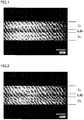
- Fig. 1 shows a micrograph of a cross section of the manufactured heat spreader. It can be seen from Fig. 1 that, in the heat spreader manufactured through the above steps, the variation in the thickness of the Cu-Mo layer was small, and the Cu-Mo layer and the Cu layers each had a substantially uniform thickness.
- the average thickness of the Cu-Mo layer determined by the aforementioned method from three cross sections including the cross section of Fig. 1 was 0.195 mm, and the variation in thickness was 0.06 mm. Furthermore, the average thicknesses of the two Cu layers determined by the same method were 0.412 mm and 0.409 m.
- the manufactured heat spreader was cut out in the shape of a disk having a diameter of 15 mm, and, to each of front and rear surfaces thereof, a chromium-molybdenum steel having a diameter of 15 mm and a length of 70 mm was bonded with silver solder. Then, a tensile test was performed using a tensile tester. Rupture occurred at not interfaces between the Cu-Mo layer and the Cu layers but portions where the chromium-molybdenum steels were bonded with the silver solder. Therefore, it was found that the strength of bonding between the Cu-Mo layer and each Cu layer is more than the rupture strength of the portions bonded with the silver solder (170 MPa).
- a heat spreader was manufactured as in Example 1, except for using an unplanarized plate material of the Cu-Mo composite body having an average thickness of 0.80 mm, a variation in thickness of 0.04 mm, and an arithmetic average roughness Ra of the both surfaces thereof of 0.1 ⁇ m.
- Fig. 2 shows a micrograph of a cross section of the manufactured heat spreader. It can be seen from Fig. 2 that, in the heat spreader manufactured without planarizing the plate material, the thickness of the Cu-Mo layer had a large variation and was not uniform, and the Cu-Mo layer partly became discontinuous.
- the average thickness of the Cu-Mo layer determined by the aforementioned method from three cross sections including the cross section of Fig. 2 was 0.184 mm, and the variation in thickness was 0.184 mm. Furthermore, the average thicknesses of the two Cu layers determined by the same method were 0.415 mm and 0.418 m.
- Each heat spreader was manufactured as in Example 1, except for changing conditions for planarization treatment and setting the variation in the thickness of the planarized plate material and the arithmetic average roughness Ra of the both surfaces thereof to values shown in Table 1 or Table 2.
- Each heat spreader was manufactured as in Example 1, except for setting the total thickness of the stacked body including a Cu-Mo layer and two Cu layers and the total rolling reduction in the hot rolling and the cold rolling to values shown in Table 1.
- Each heat spreader was manufactured as in Example 1, except for using Cu plates having thicknesses shown in Table 1 or Table 2, and setting the total thickness of the stacked body including a Cu-Mo layer and two Cu layers and the total rolling reduction in the hot rolling and the cold rolling to values shown in Table 1 or Table 2.
- Each heat spreader was manufactured as in Example 1, except for using a Cu-Mo composite material having a ratio of Cu shown in Table 2.
- Each heat spreader was manufactured as in Example 1, except for using a Cu-Mo composite material having a ratio of Cu shown in Table 2 and Cu plates having thicknesses shown in Table 2, and setting the total thickness of the stacked body including a Cu-Mo layer and two Cu layers and the total rolling reduction in the hot rolling and the cold rolling to values shown in Table 2.
- Table 1 and Table 2 list the average thickness of the Cu-Mo layer, the variation in thickness thereof, the average thicknesses of the two Cu layers, the total thickness of the heat spreader, the ratio of the thickness of the Cu-Mo layer, the total rolling reduction in the hot rolling and the cold rolling, and the like determined by the aforementioned method in the heat spreader manufactured in each of the Examples and the Comparative Examples described above.
- Example 1 Planarized Plate Material Cu Plate Heat Spreader Ratio of Cu (Vol%) Average Thickness (mm) Variation in Thickness (mm) Ra ( ⁇ m) Thickness (mm) Thickness (mm) Total Thickness (mm) Total Rolling Reduction (%) Cu Layer Cu-Mo Layer Average Thickness (mm) Average Thickness (mm) Average Thickness (mm) Variation in Thickness (mm) Ratio of Thickness (%)
- Example 1 32.9 0.80 0.010 0.010 2.00 2.00 1.02 78.8 0.412 0.409 0.195 0.060 19.2
- Example 2 32.9 0.80 0.008 0.007 2.00 2.00 1.02 78.8 0.412 0.415 0.196 0.052 19.2
- Example 3 32.9 0.80 0.005 0.005 2.00 2.00 1.02 78.8 0.410 0.413 0.194 0.032 19.1
- Example 4 32.9 0.80 0.010 0.015 2.00 2.00 1.03 78.5 0.413 0.416 0.197
- Example 19 22.0 0.80 0.010 0.010 2.00 2.00 1.01 79.0 0.413 0.410 0.191 0.058 18.8
- Example 20 22.0 0.80 0.020 0.020 2.00 2.00 1.01 79.0 0.410 0.409 0.189 0.092 18.8
- Example 21 43.0 0.80 0.010 0.010 2.00 2.00 1.02 78.8 0.413 0.412 0.197 0.043 19.3
- Example 22 43.0 0.80 0.020 0.020 2.00 2.00 2.00 1.03 78.5 0.413 0.415 0.198 0.066 19.3
- Example 23 56.0 1.00 0.010 0.010 1.20 1.20 0.40 88.2 0.135 0.134 0.134 0.031 33.3
- Example 24 56.0 1.00 0.020 0.020 1.20 1.20 0.40 88.2 0.136 0.133 0.135 0.061 33.4 Comparative Example 1 32.9 0.80 0.040 0.100 2.00 2.00 1.02 78.8 0.4
- the results of the Examples and the Comparative Examples in the both tables have revealed that, in order to set the average thickness of the Cu-Mo layer of the heat spreader to less than or equal to 0.6 mm and to set the variation in thickness to less than or equal to 0.1 mm, it is preferable to plaranize the plate material of the Cu-Mo composite material constituting the Cu-Mo layer to have an average thickness of more than or equal to 0.5 mm and less than or equal to 1.5 mm, a variation in thickness of less than or equal to 0.02 mm, and an arithmetic average roughness Ra of each of the both surfaces of less than or equal to 0.02 ⁇ m.
Landscapes
- Engineering & Computer Science (AREA)
- Physics & Mathematics (AREA)
- Chemical & Material Sciences (AREA)
- Materials Engineering (AREA)
- Mechanical Engineering (AREA)
- Microelectronics & Electronic Packaging (AREA)
- Thermal Sciences (AREA)
- Condensed Matter Physics & Semiconductors (AREA)
- General Physics & Mathematics (AREA)
- Computer Hardware Design (AREA)
- Power Engineering (AREA)
- General Engineering & Computer Science (AREA)
- Manufacturing & Machinery (AREA)
- Fluid Mechanics (AREA)
- Ceramic Engineering (AREA)
- Metallurgy (AREA)
- Organic Chemistry (AREA)
- Composite Materials (AREA)
- Chemical Kinetics & Catalysis (AREA)
- Cooling Or The Like Of Semiconductors Or Solid State Devices (AREA)
- Powder Metallurgy (AREA)
- Pressure Welding/Diffusion-Bonding (AREA)
- Laminated Bodies (AREA)
Claims (8)
- Wärmeverteiler, umfassend:eine Cu-Mo-Schicht, die aus einem Cu-Mo-Verbundmaterial gefertigt ist und eine durchschnittliche Dicke von weniger als oder gleich 0,6 mm und eine Dickenschwankung von weniger als oder gleich 0,1 mm aufweist; dadurch gekennzeichnet, dasseine Cu-Schicht direkt auf jeder der beiden Oberflächen der Cu-Mo-Schicht gestapelt ist, undwobei eine Stärke der Verbindung zwischen der Cu-Mo-Schicht und der Cu-Schicht mehr als oder gleich 150 MPa beträgt.
- Wärmeverteiler nach Anspruch 1, wobei die Cu-Mo-Schicht und die Cu-Schicht an jeder derer beiden Oberflächen direkt miteinander walzverbunden sind.
- Wärmeverteiler nach Anspruch 1 oder 2, wobei die Cu-Mo-Schicht eine durchschnittliche Dicke von mehr als oder gleich 0,12 mm aufweist.
- Wärmeverteiler nach einem der Ansprüche 1 bis 3, wobei die Cu-Mo-Schicht eine Dickenschwankung von mehr als oder gleich 0,03 mm und weniger als oder gleich 0,06 mm aufweist.
- Wärmeverteiler nach einem der Ansprüche 1 bis 4, wobei ein Verhältnis der Dicke der Cu-Mo-Schicht zu einer Gesamtdicke mehr als oder gleich 15% und weniger als oder gleich 35% beträgt.
- Wärmeverteiler nach einem der Ansprüche 1 bis 5, wobei eine Plattierung an einer äußersten Oberfläche durchgeführt wird.
- Verfahren zur Herstellung des Wärmeverteilers nach einem der Ansprüche 1 bis 6, umfassend die Schritte:Planarisieren eines Plattenmaterials des Cu-Mo-Verbundmaterials, das die Cu-Mo-Schicht bildet; und gekennzeichnet durchdirektes Walzverbinden einer Cu-Platte, die die Cu-Schicht bildet, mit jeder der beiden Oberflächen des planarisierten Plattenmaterials.
- Verfahren zur Herstellung des Wärmeverteilers nach Anspruch 7, wobei bei dem Schritt des Planarisierens das Plattenmaterial so planarisiert wird, dass es eine durchschnittliche Dicke von mehr als oder gleich 0,5 mm und weniger als oder gleich 1,5 mm, eine Dickenschwankung von weniger als oder gleich 0,02 mm und eine arithmetische mittlere Rauigkeit Ra einer Rauigkeitskurve jeder der beiden Oberflächen von weniger als oder gleich 0,02 µm aufweist.
Applications Claiming Priority (2)
| Application Number | Priority Date | Filing Date | Title |
|---|---|---|---|
| JP2014111428 | 2014-05-29 | ||
| PCT/JP2015/063811 WO2015182385A1 (ja) | 2014-05-29 | 2015-05-13 | ヒートスプレッダとその製造方法 |
Publications (3)
| Publication Number | Publication Date |
|---|---|
| EP3147384A1 EP3147384A1 (de) | 2017-03-29 |
| EP3147384A4 EP3147384A4 (de) | 2018-02-14 |
| EP3147384B1 true EP3147384B1 (de) | 2021-10-13 |
Family
ID=54698722
Family Applications (1)
| Application Number | Title | Priority Date | Filing Date |
|---|---|---|---|
| EP15798992.2A Active EP3147384B1 (de) | 2014-05-29 | 2015-05-13 | Wärmeverteiler und verfahren zur herstellung davon |
Country Status (6)
| Country | Link |
|---|---|
| US (1) | US10215512B2 (de) |
| EP (1) | EP3147384B1 (de) |
| JP (2) | JP6115900B2 (de) |
| KR (2) | KR20170010816A (de) |
| CN (1) | CN106460191B (de) |
| WO (1) | WO2015182385A1 (de) |
Families Citing this family (9)
| Publication number | Priority date | Publication date | Assignee | Title |
|---|---|---|---|---|
| EP3285950A4 (de) * | 2015-04-24 | 2018-10-10 | Engineered Materials Solutions LLC | Selbstlötendes material und verfahren zur herstellung des materials |
| JP6782561B2 (ja) * | 2015-07-16 | 2020-11-11 | Jx金属株式会社 | キャリア付銅箔、積層体、積層体の製造方法、プリント配線板の製造方法及び電子機器の製造方法 |
| JP6200042B2 (ja) | 2015-08-06 | 2017-09-20 | Jx金属株式会社 | キャリア付銅箔、積層体、プリント配線板の製造方法及び電子機器の製造方法 |
| JP6233677B1 (ja) * | 2016-08-31 | 2017-11-22 | Jfe精密株式会社 | 放熱板及びその製造方法 |
| JP6455896B1 (ja) * | 2017-11-18 | 2019-01-23 | Jfe精密株式会社 | 放熱板及びその製造方法 |
| JP6462172B1 (ja) * | 2018-08-02 | 2019-01-30 | Jfe精密株式会社 | 放熱板及びその製造方法 |
| DE112021006684T5 (de) * | 2020-12-24 | 2023-10-26 | A.L.M.T. Corp. | Verbundmaterial, Halbleiterbaugruppe, und Verfahren zur Herstellung von Verbundmaterial |
| WO2022172856A1 (ja) * | 2021-02-10 | 2022-08-18 | 住友電気工業株式会社 | 複合材料、ヒートスプレッダ及び半導体パッケージ |
| CN114406260B (zh) * | 2021-12-24 | 2024-03-05 | 海特信科新材料科技有限公司 | 一种高可靠性cpc复合材料的生产工艺 |
Family Cites Families (17)
| Publication number | Priority date | Publication date | Assignee | Title |
|---|---|---|---|---|
| US5493153A (en) | 1992-11-26 | 1996-02-20 | Tokyo Tungsten Co., Ltd. | Plastic-packaged semiconductor device having a heat sink matched with a plastic package |
| JP2704932B2 (ja) | 1993-03-11 | 1998-01-26 | 東京タングステン株式会社 | 放熱基板およびその製造方法ならびに半導体装置 |
| JPH06268117A (ja) * | 1993-03-15 | 1994-09-22 | Sumitomo Electric Ind Ltd | 半導体装置用放熱基板およびその製造方法 |
| JPH11297909A (ja) * | 1998-04-10 | 1999-10-29 | Sumitomo Metal Electronics Devices Inc | 放熱用金属板およびそれを用いた電子部品用パッケージ |
| JP3479738B2 (ja) * | 1998-11-16 | 2003-12-15 | 株式会社アライドマテリアル | 半導体パッケージと、それに用いる放熱基板の製造方法 |
| US20010038140A1 (en) * | 2000-04-06 | 2001-11-08 | Karker Jeffrey A. | High rigidity, multi-layered semiconductor package and method of making the same |
| JP2001358226A (ja) | 2000-06-14 | 2001-12-26 | Asahi Kasei Microsystems Kk | アナログ回路及びその製造方法 |
| JP2004281676A (ja) * | 2003-03-14 | 2004-10-07 | Toyota Motor Corp | 放熱板及び放熱板の製造方法 |
| JP2007142126A (ja) | 2005-11-18 | 2007-06-07 | Allied Material Corp | 複合材料及び半導体搭載用放熱基板、及びそれを用いたセラミックパッケージ |
| JP5028147B2 (ja) * | 2007-05-29 | 2012-09-19 | 株式会社アライドマテリアル | 半導体装置用ヒートスプレッダとその製造方法 |
| US20080298024A1 (en) | 2007-05-31 | 2008-12-04 | A.L.M.T. Corp. | Heat spreader and method for manufacturing the same, and semiconductor device |
| JP4876097B2 (ja) * | 2007-05-31 | 2012-02-15 | 株式会社アライドマテリアル | ヒートスプレッダとその製造方法および半導体装置 |
| JP4382154B2 (ja) * | 2008-02-06 | 2009-12-09 | 株式会社アライドマテリアル | ヒートスプレッダおよびその製造方法 |
| JP5124330B2 (ja) * | 2008-03-26 | 2013-01-23 | 新電元工業株式会社 | 半導体装置 |
| JP5198982B2 (ja) * | 2008-09-03 | 2013-05-15 | 株式会社アライドマテリアル | ヒートスプレッダおよびその製造方法 |
| CN102284701B (zh) | 2011-08-26 | 2012-10-03 | 西北有色金属研究院 | 一种Cu-MoCu-Cu复合板材的制备方法 |
| CN102941702B (zh) * | 2012-12-04 | 2015-02-11 | 西北有色金属研究院 | 一种Cu-MoCu-Cu三层复合板材的熔渗制备方法 |
-
2015
- 2015-05-13 US US15/312,931 patent/US10215512B2/en active Active
- 2015-05-13 JP JP2015545219A patent/JP6115900B2/ja active Active
- 2015-05-13 WO PCT/JP2015/063811 patent/WO2015182385A1/ja active Application Filing
- 2015-05-13 CN CN201580028494.7A patent/CN106460191B/zh active Active
- 2015-05-13 EP EP15798992.2A patent/EP3147384B1/de active Active
- 2015-05-13 KR KR1020167035794A patent/KR20170010816A/ko not_active Application Discontinuation
- 2015-05-13 KR KR1020187028887A patent/KR20180114231A/ko not_active Application Discontinuation
-
2016
- 2016-09-01 JP JP2016171083A patent/JP2017028295A/ja active Pending
Non-Patent Citations (1)
| Title |
|---|
| None * |
Also Published As
| Publication number | Publication date |
|---|---|
| WO2015182385A1 (ja) | 2015-12-03 |
| US20170198991A1 (en) | 2017-07-13 |
| JP6115900B2 (ja) | 2017-04-19 |
| JPWO2015182385A1 (ja) | 2017-04-20 |
| US10215512B2 (en) | 2019-02-26 |
| CN106460191A (zh) | 2017-02-22 |
| KR20180114231A (ko) | 2018-10-17 |
| EP3147384A4 (de) | 2018-02-14 |
| CN106460191B (zh) | 2019-01-04 |
| JP2017028295A (ja) | 2017-02-02 |
| EP3147384A1 (de) | 2017-03-29 |
| KR20170010816A (ko) | 2017-02-01 |
Similar Documents
| Publication | Publication Date | Title |
|---|---|---|
| EP3147384B1 (de) | Wärmeverteiler und verfahren zur herstellung davon | |
| EP3629370B1 (de) | Schaltkreissubstrat und halbleiterbauelement | |
| EP3285292B1 (de) | Verbundener körper, substrat für ein leistungsmodul mit einem kühlkörper, kühlkörper, verfahren zur herstellung des verbundenen körpers, verfahren zur herstellung des substrats für ein leistungsmodul mit einem kühlkörper und verfahren zur herstellung eines kühlkörpers | |
| EP3285291B1 (de) | Verbundener körper, substrat für ein leistungsmodul mit einem kühlkörper, kühlkörper, verfahren zur herstellung des verbundenen körpers, verfahren zur herstellung des substrats für ein leistungsmodul mit einem kühlkörper und verfahren zur herstellung eines kühlkörpers | |
| JP5698947B2 (ja) | 電子機器用放熱板およびその製造方法 | |
| EP3509100B1 (de) | Kühlkörper und verfahren zu herstellung davon | |
| US9984951B2 (en) | Sintered multilayer heat sinks for microelectronic packages and methods for the production thereof | |
| WO2007074720A1 (ja) | 半導体素子実装用基板とそれを用いた半導体装置および半導体素子実装用基板の製造方法 | |
| EP2690186A1 (de) | Verbundbauteil mit einem aus einem verbundwerkstoff geformten substrat | |
| US20180328677A1 (en) | Heat-dissipating plate for high-power element | |
| JP5531329B2 (ja) | 半導体用放熱部品を基体とするパッケージ | |
| EP3605601B1 (de) | Verfahren zur herstellung einer isolierten leiterplatte mit kühlkörper | |
| EP3888836A1 (de) | Verbundkörper, an kühlkörper befestigte, isolierte leiterplatte und kühlkörper | |
| JP7440944B2 (ja) | 複合材料および放熱部品 | |
| US10497585B2 (en) | Bonded body, substrate for power module with heat sink, heat sink, method for producing bonded body, method for producing substrate for power module with heat sink, and method for producing heat sink | |
| JP4055596B2 (ja) | 複合材 | |
| JP6429108B2 (ja) | 半導体素子実装用基板とそれを用いた半導体素子装置 |
Legal Events
| Date | Code | Title | Description |
|---|---|---|---|
| STAA | Information on the status of an ep patent application or granted ep patent |
Free format text: STATUS: THE INTERNATIONAL PUBLICATION HAS BEEN MADE |
|
| PUAI | Public reference made under article 153(3) epc to a published international application that has entered the european phase |
Free format text: ORIGINAL CODE: 0009012 |
|
| STAA | Information on the status of an ep patent application or granted ep patent |
Free format text: STATUS: REQUEST FOR EXAMINATION WAS MADE |
|
| 17P | Request for examination filed |
Effective date: 20161220 |
|
| AK | Designated contracting states |
Kind code of ref document: A1 Designated state(s): AL AT BE BG CH CY CZ DE DK EE ES FI FR GB GR HR HU IE IS IT LI LT LU LV MC MK MT NL NO PL PT RO RS SE SI SK SM TR |
|
| AX | Request for extension of the european patent |
Extension state: BA ME |
|
| DAV | Request for validation of the european patent (deleted) | ||
| DAX | Request for extension of the european patent (deleted) | ||
| A4 | Supplementary search report drawn up and despatched |
Effective date: 20180117 |
|
| RIC1 | Information provided on ipc code assigned before grant |
Ipc: C23C 26/00 20060101AFI20180110BHEP Ipc: B23K 20/04 20060101ALI20180110BHEP Ipc: C22C 9/00 20060101ALI20180110BHEP Ipc: C22C 27/04 20060101ALI20180110BHEP Ipc: B22F 7/06 20060101ALI20180110BHEP Ipc: H01L 23/373 20060101ALI20180110BHEP Ipc: B22F 3/10 20060101ALI20180110BHEP Ipc: B32B 15/01 20060101ALI20180110BHEP |
|
| STAA | Information on the status of an ep patent application or granted ep patent |
Free format text: STATUS: EXAMINATION IS IN PROGRESS |
|
| 17Q | First examination report despatched |
Effective date: 20181113 |
|
| RIC1 | Information provided on ipc code assigned before grant |
Ipc: H01L 23/373 20060101ALI20200420BHEP Ipc: F28F 13/00 20060101ALI20200420BHEP Ipc: C22C 27/04 20060101ALI20200420BHEP Ipc: B22F 3/10 20060101ALI20200420BHEP Ipc: C23C 26/00 20060101AFI20200420BHEP Ipc: F28F 21/08 20060101ALI20200420BHEP Ipc: B22F 7/06 20060101ALI20200420BHEP Ipc: B32B 15/01 20060101ALI20200420BHEP Ipc: C22C 9/00 20060101ALI20200420BHEP Ipc: B23K 20/04 20060101ALI20200420BHEP |
|
| STAA | Information on the status of an ep patent application or granted ep patent |
Free format text: STATUS: EXAMINATION IS IN PROGRESS |
|
| GRAP | Despatch of communication of intention to grant a patent |
Free format text: ORIGINAL CODE: EPIDOSNIGR1 |
|
| STAA | Information on the status of an ep patent application or granted ep patent |
Free format text: STATUS: GRANT OF PATENT IS INTENDED |
|
| INTG | Intention to grant announced |
Effective date: 20210528 |
|
| GRAS | Grant fee paid |
Free format text: ORIGINAL CODE: EPIDOSNIGR3 |
|
| GRAA | (expected) grant |
Free format text: ORIGINAL CODE: 0009210 |
|
| STAA | Information on the status of an ep patent application or granted ep patent |
Free format text: STATUS: THE PATENT HAS BEEN GRANTED |
|
| AK | Designated contracting states |
Kind code of ref document: B1 Designated state(s): AL AT BE BG CH CY CZ DE DK EE ES FI FR GB GR HR HU IE IS IT LI LT LU LV MC MK MT NL NO PL PT RO RS SE SI SK SM TR |
|
| REG | Reference to a national code |
Ref country code: GB Ref legal event code: FG4D |
|
| REG | Reference to a national code |
Ref country code: CH Ref legal event code: EP |
|
| REG | Reference to a national code |
Ref country code: DE Ref legal event code: R096 Ref document number: 602015074131 Country of ref document: DE |
|
| REG | Reference to a national code |
Ref country code: IE Ref legal event code: FG4D |
|
| REG | Reference to a national code |
Ref country code: AT Ref legal event code: REF Ref document number: 1438245 Country of ref document: AT Kind code of ref document: T Effective date: 20211115 |
|
| REG | Reference to a national code |
Ref country code: LT Ref legal event code: MG9D |
|
| REG | Reference to a national code |
Ref country code: NL Ref legal event code: MP Effective date: 20211013 |
|
| PG25 | Lapsed in a contracting state [announced via postgrant information from national office to epo] |
Ref country code: RS Free format text: LAPSE BECAUSE OF FAILURE TO SUBMIT A TRANSLATION OF THE DESCRIPTION OR TO PAY THE FEE WITHIN THE PRESCRIBED TIME-LIMIT Effective date: 20211013 Ref country code: LT Free format text: LAPSE BECAUSE OF FAILURE TO SUBMIT A TRANSLATION OF THE DESCRIPTION OR TO PAY THE FEE WITHIN THE PRESCRIBED TIME-LIMIT Effective date: 20211013 Ref country code: FI Free format text: LAPSE BECAUSE OF FAILURE TO SUBMIT A TRANSLATION OF THE DESCRIPTION OR TO PAY THE FEE WITHIN THE PRESCRIBED TIME-LIMIT Effective date: 20211013 Ref country code: BG Free format text: LAPSE BECAUSE OF FAILURE TO SUBMIT A TRANSLATION OF THE DESCRIPTION OR TO PAY THE FEE WITHIN THE PRESCRIBED TIME-LIMIT Effective date: 20220113 |
|
| PG25 | Lapsed in a contracting state [announced via postgrant information from national office to epo] |
Ref country code: IS Free format text: LAPSE BECAUSE OF FAILURE TO SUBMIT A TRANSLATION OF THE DESCRIPTION OR TO PAY THE FEE WITHIN THE PRESCRIBED TIME-LIMIT Effective date: 20220213 Ref country code: SE Free format text: LAPSE BECAUSE OF FAILURE TO SUBMIT A TRANSLATION OF THE DESCRIPTION OR TO PAY THE FEE WITHIN THE PRESCRIBED TIME-LIMIT Effective date: 20211013 Ref country code: PT Free format text: LAPSE BECAUSE OF FAILURE TO SUBMIT A TRANSLATION OF THE DESCRIPTION OR TO PAY THE FEE WITHIN THE PRESCRIBED TIME-LIMIT Effective date: 20220214 Ref country code: PL Free format text: LAPSE BECAUSE OF FAILURE TO SUBMIT A TRANSLATION OF THE DESCRIPTION OR TO PAY THE FEE WITHIN THE PRESCRIBED TIME-LIMIT Effective date: 20211013 Ref country code: NO Free format text: LAPSE BECAUSE OF FAILURE TO SUBMIT A TRANSLATION OF THE DESCRIPTION OR TO PAY THE FEE WITHIN THE PRESCRIBED TIME-LIMIT Effective date: 20220113 Ref country code: NL Free format text: LAPSE BECAUSE OF FAILURE TO SUBMIT A TRANSLATION OF THE DESCRIPTION OR TO PAY THE FEE WITHIN THE PRESCRIBED TIME-LIMIT Effective date: 20211013 Ref country code: LV Free format text: LAPSE BECAUSE OF FAILURE TO SUBMIT A TRANSLATION OF THE DESCRIPTION OR TO PAY THE FEE WITHIN THE PRESCRIBED TIME-LIMIT Effective date: 20211013 Ref country code: HR Free format text: LAPSE BECAUSE OF FAILURE TO SUBMIT A TRANSLATION OF THE DESCRIPTION OR TO PAY THE FEE WITHIN THE PRESCRIBED TIME-LIMIT Effective date: 20211013 Ref country code: GR Free format text: LAPSE BECAUSE OF FAILURE TO SUBMIT A TRANSLATION OF THE DESCRIPTION OR TO PAY THE FEE WITHIN THE PRESCRIBED TIME-LIMIT Effective date: 20220114 Ref country code: ES Free format text: LAPSE BECAUSE OF FAILURE TO SUBMIT A TRANSLATION OF THE DESCRIPTION OR TO PAY THE FEE WITHIN THE PRESCRIBED TIME-LIMIT Effective date: 20211013 |
|
| REG | Reference to a national code |
Ref country code: DE Ref legal event code: R097 Ref document number: 602015074131 Country of ref document: DE |
|
| PG25 | Lapsed in a contracting state [announced via postgrant information from national office to epo] |
Ref country code: SM Free format text: LAPSE BECAUSE OF FAILURE TO SUBMIT A TRANSLATION OF THE DESCRIPTION OR TO PAY THE FEE WITHIN THE PRESCRIBED TIME-LIMIT Effective date: 20211013 Ref country code: SK Free format text: LAPSE BECAUSE OF FAILURE TO SUBMIT A TRANSLATION OF THE DESCRIPTION OR TO PAY THE FEE WITHIN THE PRESCRIBED TIME-LIMIT Effective date: 20211013 Ref country code: RO Free format text: LAPSE BECAUSE OF FAILURE TO SUBMIT A TRANSLATION OF THE DESCRIPTION OR TO PAY THE FEE WITHIN THE PRESCRIBED TIME-LIMIT Effective date: 20211013 Ref country code: EE Free format text: LAPSE BECAUSE OF FAILURE TO SUBMIT A TRANSLATION OF THE DESCRIPTION OR TO PAY THE FEE WITHIN THE PRESCRIBED TIME-LIMIT Effective date: 20211013 Ref country code: DK Free format text: LAPSE BECAUSE OF FAILURE TO SUBMIT A TRANSLATION OF THE DESCRIPTION OR TO PAY THE FEE WITHIN THE PRESCRIBED TIME-LIMIT Effective date: 20211013 Ref country code: CZ Free format text: LAPSE BECAUSE OF FAILURE TO SUBMIT A TRANSLATION OF THE DESCRIPTION OR TO PAY THE FEE WITHIN THE PRESCRIBED TIME-LIMIT Effective date: 20211013 |
|
| PLBE | No opposition filed within time limit |
Free format text: ORIGINAL CODE: 0009261 |
|
| STAA | Information on the status of an ep patent application or granted ep patent |
Free format text: STATUS: NO OPPOSITION FILED WITHIN TIME LIMIT |
|
| 26N | No opposition filed |
Effective date: 20220714 |
|
| PG25 | Lapsed in a contracting state [announced via postgrant information from national office to epo] |
Ref country code: AL Free format text: LAPSE BECAUSE OF FAILURE TO SUBMIT A TRANSLATION OF THE DESCRIPTION OR TO PAY THE FEE WITHIN THE PRESCRIBED TIME-LIMIT Effective date: 20211013 |
|
| PG25 | Lapsed in a contracting state [announced via postgrant information from national office to epo] |
Ref country code: SI Free format text: LAPSE BECAUSE OF FAILURE TO SUBMIT A TRANSLATION OF THE DESCRIPTION OR TO PAY THE FEE WITHIN THE PRESCRIBED TIME-LIMIT Effective date: 20211013 |
|
| REG | Reference to a national code |
Ref country code: CH Ref legal event code: PL |
|
| REG | Reference to a national code |
Ref country code: BE Ref legal event code: MM Effective date: 20220531 |
|
| GBPC | Gb: european patent ceased through non-payment of renewal fee |
Effective date: 20220513 |
|
| PG25 | Lapsed in a contracting state [announced via postgrant information from national office to epo] |
Ref country code: MC Free format text: LAPSE BECAUSE OF FAILURE TO SUBMIT A TRANSLATION OF THE DESCRIPTION OR TO PAY THE FEE WITHIN THE PRESCRIBED TIME-LIMIT Effective date: 20211013 Ref country code: LU Free format text: LAPSE BECAUSE OF NON-PAYMENT OF DUE FEES Effective date: 20220513 Ref country code: LI Free format text: LAPSE BECAUSE OF NON-PAYMENT OF DUE FEES Effective date: 20220531 Ref country code: CH Free format text: LAPSE BECAUSE OF NON-PAYMENT OF DUE FEES Effective date: 20220531 |
|
| REG | Reference to a national code |
Ref country code: AT Ref legal event code: UEP Ref document number: 1438245 Country of ref document: AT Kind code of ref document: T Effective date: 20211013 |
|
| PG25 | Lapsed in a contracting state [announced via postgrant information from national office to epo] |
Ref country code: IE Free format text: LAPSE BECAUSE OF NON-PAYMENT OF DUE FEES Effective date: 20220513 Ref country code: FR Free format text: LAPSE BECAUSE OF NON-PAYMENT OF DUE FEES Effective date: 20220531 |
|
| PG25 | Lapsed in a contracting state [announced via postgrant information from national office to epo] |
Ref country code: IT Free format text: LAPSE BECAUSE OF FAILURE TO SUBMIT A TRANSLATION OF THE DESCRIPTION OR TO PAY THE FEE WITHIN THE PRESCRIBED TIME-LIMIT Effective date: 20211013 Ref country code: GB Free format text: LAPSE BECAUSE OF NON-PAYMENT OF DUE FEES Effective date: 20220513 Ref country code: BE Free format text: LAPSE BECAUSE OF NON-PAYMENT OF DUE FEES Effective date: 20220531 |
|
| P01 | Opt-out of the competence of the unified patent court (upc) registered |
Effective date: 20230515 |
|
| PGFP | Annual fee paid to national office [announced via postgrant information from national office to epo] |
Ref country code: DE Payment date: 20230331 Year of fee payment: 9 |
|
| PGFP | Annual fee paid to national office [announced via postgrant information from national office to epo] |
Ref country code: AT Payment date: 20230425 Year of fee payment: 9 |
|
| PG25 | Lapsed in a contracting state [announced via postgrant information from national office to epo] |
Ref country code: HU Free format text: LAPSE BECAUSE OF FAILURE TO SUBMIT A TRANSLATION OF THE DESCRIPTION OR TO PAY THE FEE WITHIN THE PRESCRIBED TIME-LIMIT; INVALID AB INITIO Effective date: 20150513 |
|
| PG25 | Lapsed in a contracting state [announced via postgrant information from national office to epo] |
Ref country code: MK Free format text: LAPSE BECAUSE OF FAILURE TO SUBMIT A TRANSLATION OF THE DESCRIPTION OR TO PAY THE FEE WITHIN THE PRESCRIBED TIME-LIMIT Effective date: 20211013 Ref country code: CY Free format text: LAPSE BECAUSE OF FAILURE TO SUBMIT A TRANSLATION OF THE DESCRIPTION OR TO PAY THE FEE WITHIN THE PRESCRIBED TIME-LIMIT Effective date: 20211013 |